Embed Size (px)
Citation preview
INT page 1July 29, 2004
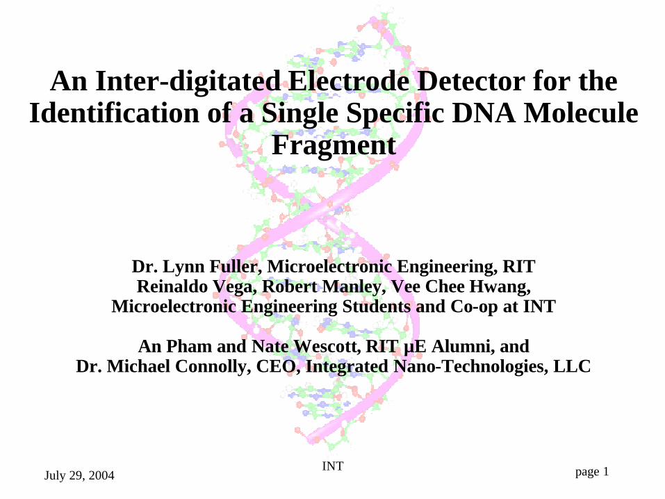
An Inter-digitated Electrode Detector for the Identification of a Single Specific DNA Molecule
Fragment
Dr. Lynn Fuller, Microelectronic Engineering, RITReinaldo Vega, Robert Manley, Vee Chee Hwang,
Microelectronic Engineering Students and Co-op at INT
An Pham and Nate Wescott, RIT µE Alumni, and Dr. Michael Connolly, CEO, Integrated Nano-Technologies, LLC
INT page 2July 29, 2004
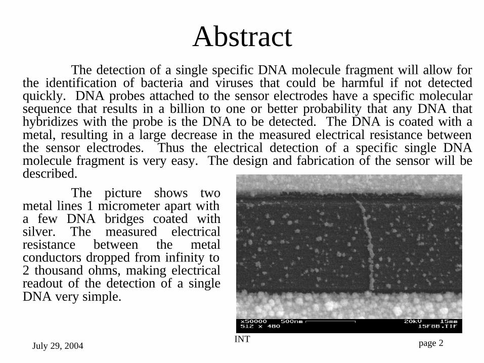
AbstractThe detection of a single specific DNA molecule fragment will allow for
the identification of bacteria and viruses that could be harmful if not detected quickly. DNA probes attached to the sensor electrodes have a specific molecular sequence that results in a billion to one or better probability that any DNA that hybridizes with the probe is the DNA to be detected. The DNA is coated with a metal, resulting in a large decrease in the measured electrical resistance between the sensor electrodes. Thus the electrical detection of a specific single DNA molecule fragment is very easy. The design and fabrication of the sensor will be described.
The picture shows two metal lines 1 micrometer apart with a few DNA bridges coated with silver. The measured electrical resistance between the metal conductors dropped from infinity to 2 thousand ohms, making electrical readout of the detection of a single DNA very simple.
INT page 3July 29, 2004
OutlineAbstractOutlineDNA PrimerMotivationDesign and LayoutWafer FabricationTesting and YieldProbesHybridizationSilver Coating of DNAElectrical Measurement of Silver Coated DNASystem DesignSummaryAcknowledgements
INT page 4July 29, 2004
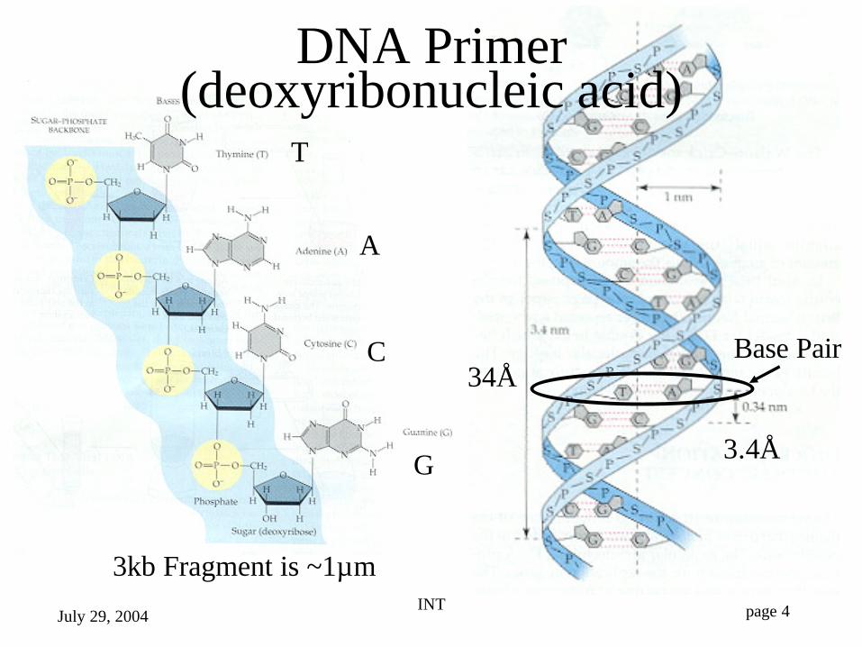
DNA Primer(deoxyribonucleic acid)
3.4Å
34ÅBase Pair
T
A
G
C
3kb Fragment is ~1µm

INT page 5July 29, 2004
TerminologyDNA – deoxyribonucleic acidBase – one of four nucleic acids adenine (A), guanine (G), cytosine (C), or thymine (T)Base Pair – A is always bonded to T, G is always bonded to CMolecule Fragment Length – stated in Kb (Kilo base pairs, each 0.34 nm)PCR – Polymerase chain reaction, is a particular reaction sequence that starts with an original DNA molecule and creates an exponentially growing population of copies of fragments of that molecule.Denaturing - at temperatures ~ 95°C double stranded DNA separates into two single stranded DNA molecules.Primer or Probes – synthetically produced single strand molecule with a specific target sequence of bases.Annealing or Hybridization – Complementary DNA molecule fragments attach to one another, done at ~65°C
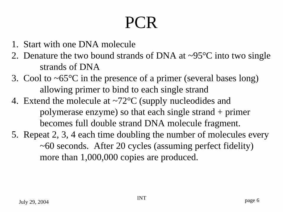
INT page 6July 29, 2004
PCR1. Start with one DNA molecule2. Denature the two bound strands of DNA at ~95°C into two single
strands of DNA3. Cool to ~65°C in the presence of a primer (several bases long)
allowing primer to bind to each single strand4. Extend the molecule at ~72°C (supply nucleodides and
polymerase enzyme) so that each single strand + primer becomes full double strand DNA molecule fragment.
5. Repeat 2, 3, 4 each time doubling the number of molecules every ~60 seconds. After 20 cycles (assuming perfect fidelity) more than 1,000,000 copies are produced.

INT page 7July 29, 2004
Sensor Based on PCR and Mechanical Stress

INT page 8July 29, 2004
Sensor Based on PCR and Mechanical Resonant Structures
The two cantilever structures have piezoresistive sensors to measure the resonant frequency of the beams. The beams have a DNA probes at the end of the cantilever that hybridizes with specific DNA molecule fragments. The additional mass is detected by a change in the resonant frequency. This type of detector requires PCR to have enough molecules to cause a change.
INT page 9July 29, 2004
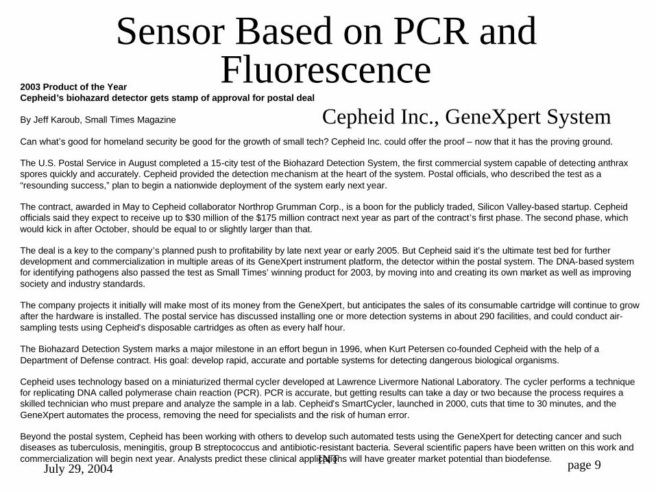
Sensor Based on PCR and Fluorescence
Cepheid Inc., GeneXpert System
2003 Product of the YearCepheid’s biohazard detector gets stamp of approval for postal deal
By Jeff Karoub, Small Times Magazine
Can what’s good for homeland security be good for the growth of small tech? Cepheid Inc. could offer the proof – now that it has the proving ground.
The U.S. Postal Service in August completed a 15-city test of the Biohazard Detection System, the first commercial system capable of detecting anthrax spores quickly and accurately. Cepheid provided the detection mechanism at the heart of the system. Postal officials, who described the test as a “resounding success,” plan to begin a nationwide deployment of the system early next year.
The contract, awarded in May to Cepheid collaborator Northrop Grumman Corp., is a boon for the publicly traded, Silicon Valley-based startup. Cepheid officials said they expect to receive up to $30 million of the $175 million contract next year as part of the contract’s first phase. The second phase, which would kick in after October, should be equal to or slightly larger than that.
The deal is a key to the company’s planned push to profitability by late next year or early 2005. But Cepheid said it’s the ultimate test bed for further development and commercialization in multiple areas of its GeneXpert instrument platform, the detector within the postal system. The DNA-based system for identifying pathogens also passed the test as Small Times’ winning product for 2003, by moving into and creating its own market as well as improving society and industry standards.
The company projects it initially will make most of its money from the GeneXpert, but anticipates the sales of its consumable cartridge will continue to grow after the hardware is installed. The postal service has discussed installing one or more detection systems in about 290 facilities, and could conduct air-sampling tests using Cepheid’s disposable cartridges as often as every half hour.
The Biohazard Detection System marks a major milestone in an effort begun in 1996, when Kurt Petersen co-founded Cepheid with the help of a Department of Defense contract. His goal: develop rapid, accurate and portable systems for detecting dangerous biological organisms.
Cepheid uses technology based on a miniaturized thermal cycler developed at Lawrence Livermore National Laboratory. The cycler performs a technique for replicating DNA called polymerase chain reaction (PCR). PCR is accurate, but getting results can take a day or two because the process requires a skilled technician who must prepare and analyze the sample in a lab. Cepheid’s SmartCycler, launched in 2000, cuts that time to 30 minutes, and theGeneXpert automates the process, removing the need for specialists and the risk of human error.
Beyond the postal system, Cepheid has been working with others to develop such automated tests using the GeneXpert for detecting cancer and such diseases as tuberculosis, meningitis, group B streptococcus and antibiotic-resistant bacteria. Several scientific papers have been written on this work and commercialization will begin next year. Analysts predict these clinical applications will have greater market potential than biodefense.

INT page 10July 29, 2004
Motivation• Biological agents such as anthrax, small pox, and tularemia havebeen developed as weapons. Even non-weaponized forms of these agents could spread to pandemic proportions if unchecked.
• Current biosensor technologies are either PCR-based (accurate but slow and requires highly skilled operator and laboratory environment) or Assay-based (portable, rapid but not accurate or sensitive)
• The sensor described in this talk is fast, accurate and very sensitive. It does not require a highly skilled operator or laboratory environment.
INT page 11July 29, 2004
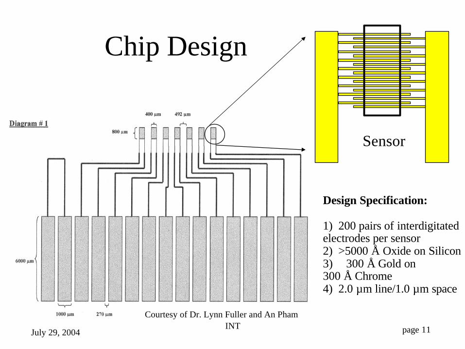
Chip Design
Design Specification:
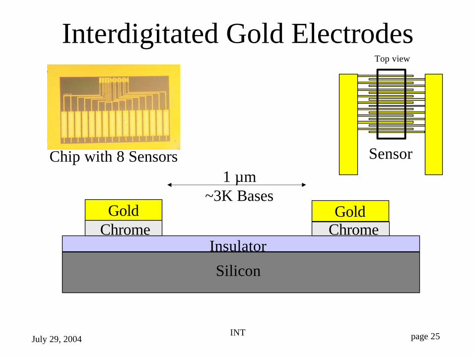
1) 200 pairs of interdigitated electrodes per sensor2) >5000 Å Oxide on Silicon3) 300 Å Gold on 300 Å Chrome 4) 2.0 µm line/1.0 µm space
Courtesy of Dr. Lynn Fuller and An Pham
Sensor
INT page 12July 29, 2004
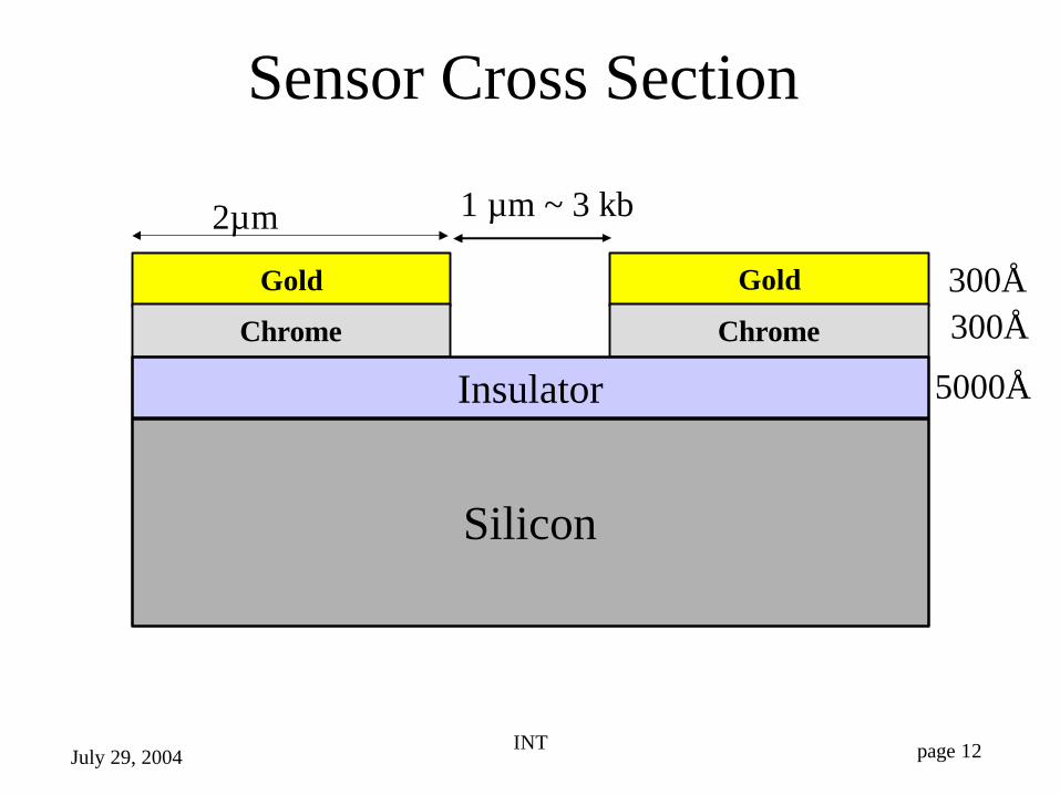
Sensor Cross Section
Gold
1 µm ~ 3 kb
Gold
Silicon
Chrome Chrome
Insulator
300Å300Å
5000Å
2µm
INT page 13July 29, 2004
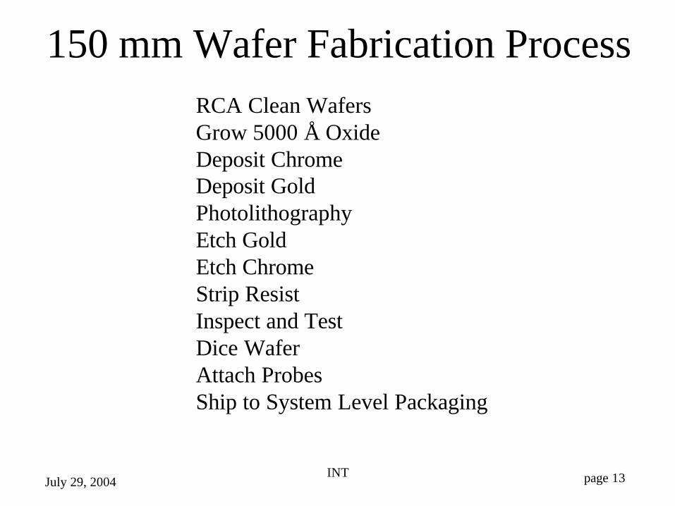
150 mm Wafer Fabrication ProcessRCA Clean WafersGrow 5000 Å OxideDeposit ChromeDeposit GoldPhotolithographyEtch GoldEtch ChromeStrip ResistInspect and TestDice Wafer Attach ProbesShip to System Level Packaging
INT page 14July 29, 2004
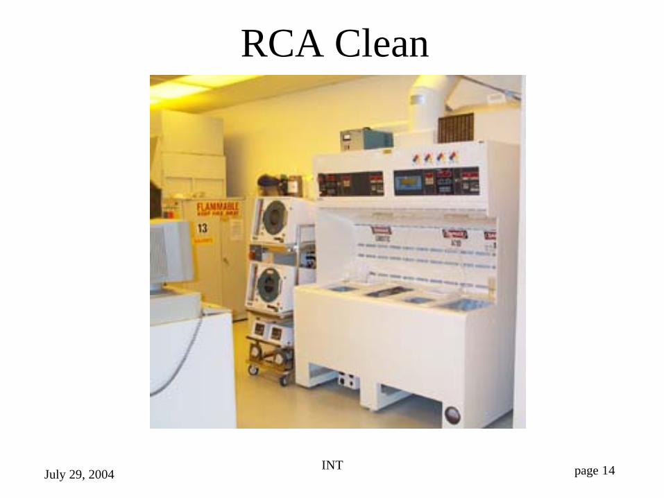
RCA Clean
INT page 15July 29, 2004
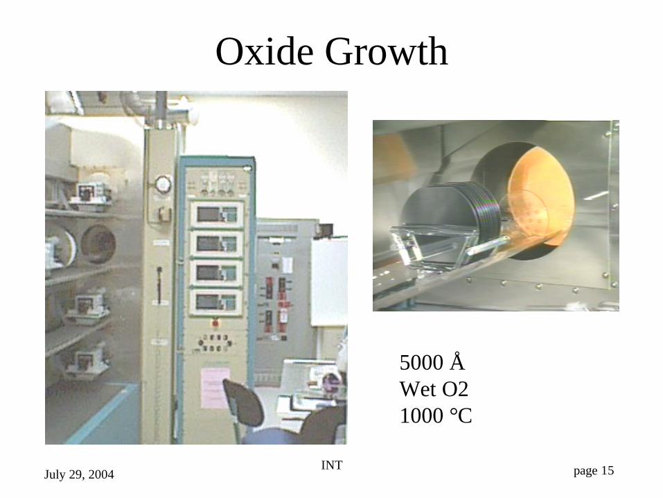
Oxide Growth
5000 ÅWet O21000 °C

INT page 16July 29, 2004
Metal Deposition
Current
Substrate
f = m4d π h2f h
f = film thicknessd = densityh = heightm = mass
Diagram courtesy of Dr. Lynn Fuller
CVC Evaporator
INT page 17July 29, 2004
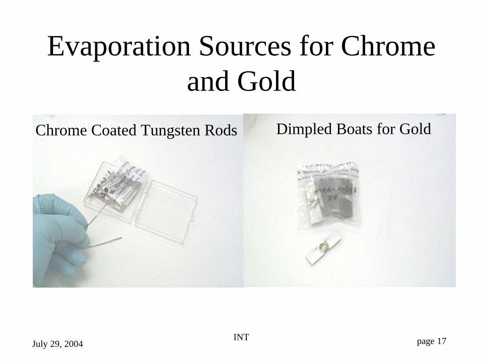
Evaporation Sources for Chrome and Gold
Chrome Coated Tungsten Rods Dimpled Boats for Gold

INT page 18July 29, 2004
Sputtering of Other Electrode Metals
CVC 601 Sputtering Tool

INT page 19July 29, 2004
Insulating Layer, Chromium and Gold
Gold
Silicon
Chrome
Insulator
300Å300Å
5000Å
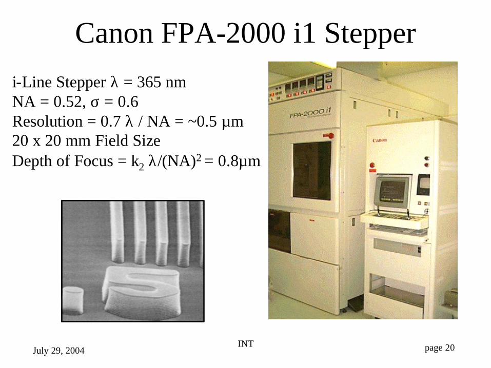
INT page 20July 29, 2004
Canon FPA-2000 i1 Stepperi-Line Stepper λ = 365 nmNA = 0.52, σ = 0.6Resolution = 0.7 λ / NA = ~0.5 µm20 x 20 mm Field SizeDepth of Focus = k2 λ/(NA)2 = 0.8µm
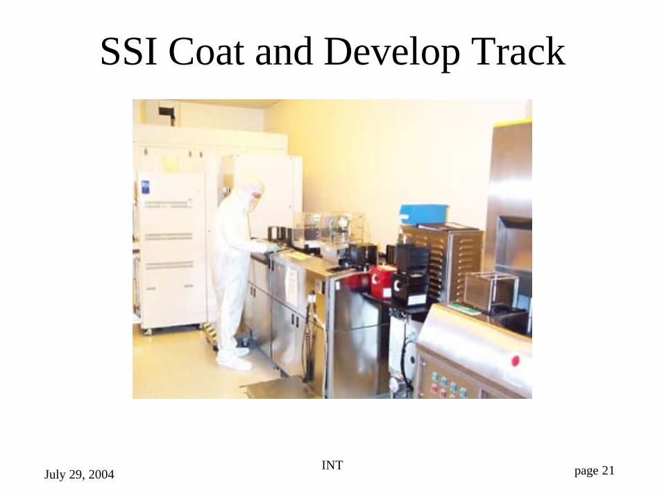
INT page 21July 29, 2004
SSI Coat and Develop Track
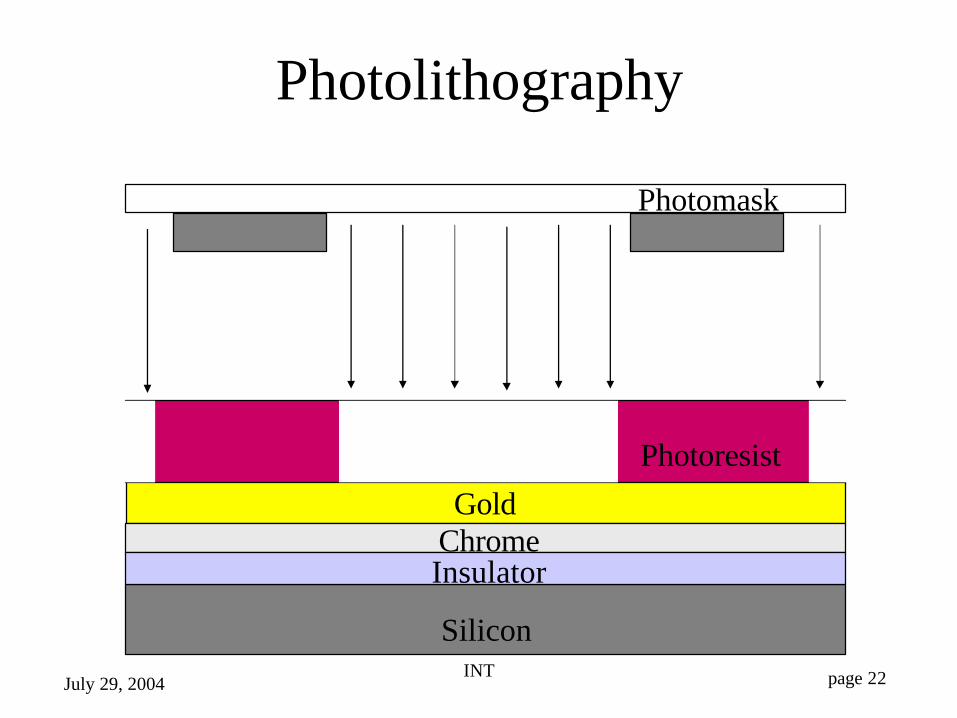
INT page 22July 29, 2004
Photolithography
GoldChromeInsulator
Silicon
Photoresist
Photomask
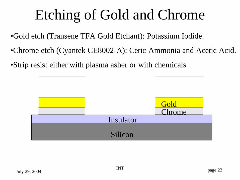
INT page 23July 29, 2004
Etching of Gold and Chrome
ChromeInsulator
Silicon
Photoresist
Gold
•Gold etch (Transene TFA Gold Etchant): Potassium Iodide.
•Chrome etch (Cyantek CE8002-A): Ceric Ammonia and Acetic Acid.
•Strip resist either with plasma asher or with chemicals

INT page 24July 29, 2004
Branson Plasma Asher
INT page 25July 29, 2004
Interdigitated Gold Electrodes
Gold Gold
1 µm~3K Bases
InsulatorChromeChrome
Silicon
Top view
SensorChip with 8 Sensors

INT page 26July 29, 2004
Picture of Interdigitated Electrodes
Sensors150X20X
INT page 27July 29, 2004
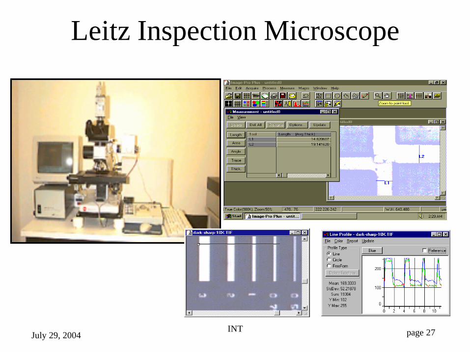
Leitz Inspection Microscope
INT page 28July 29, 2004
Testing•Each device is tested both visually and electrically.
Ω
R = ∞
Good
Ω
R = ∞
BadNo Electrodes(Over Etch)
Ω
R = low
Bad(Poor Adhesion)
Ω
R = low
Bad(Under Etch)
INT page 29July 29, 2004
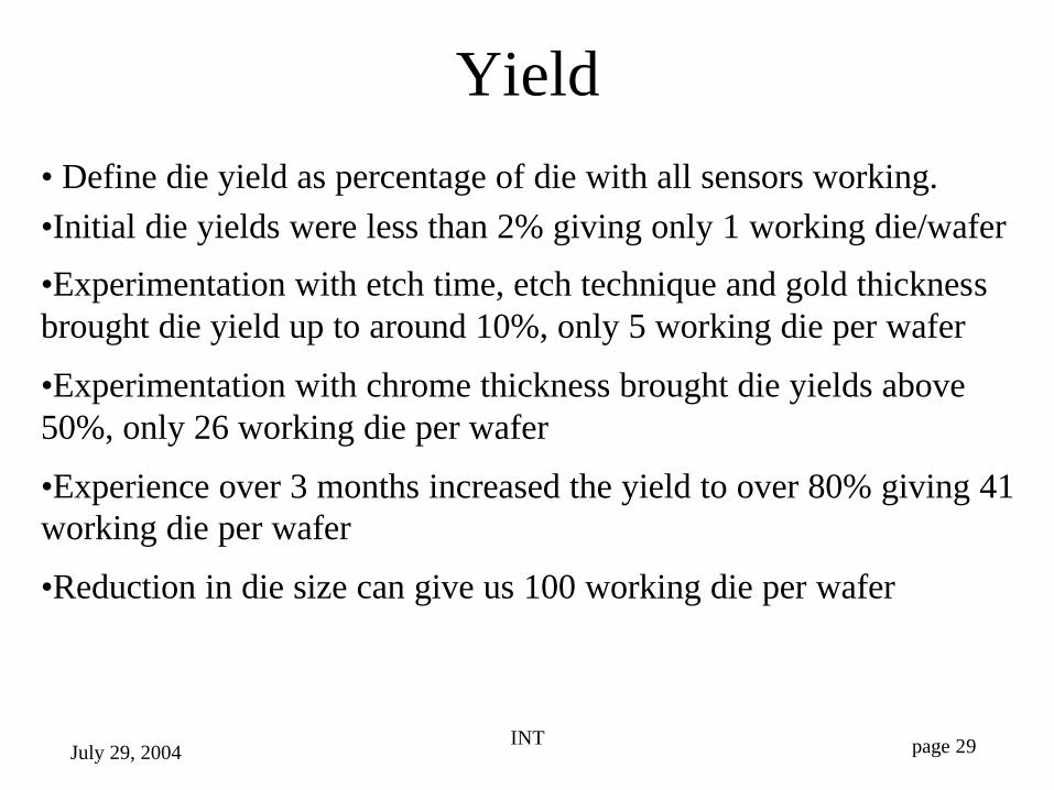
Yield• Define die yield as percentage of die with all sensors working.•Initial die yields were less than 2% giving only 1 working die/wafer
•Experimentation with etch time, etch technique and gold thickness brought die yield up to around 10%, only 5 working die per wafer
•Experimentation with chrome thickness brought die yields above 50%, only 26 working die per wafer
•Experience over 3 months increased the yield to over 80% giving 41 working die per wafer
•Reduction in die size can give us 100 working die per wafer

INT page 30July 29, 2004
Completed Wafer
Picture of Wafer
INT page 31July 29, 2004
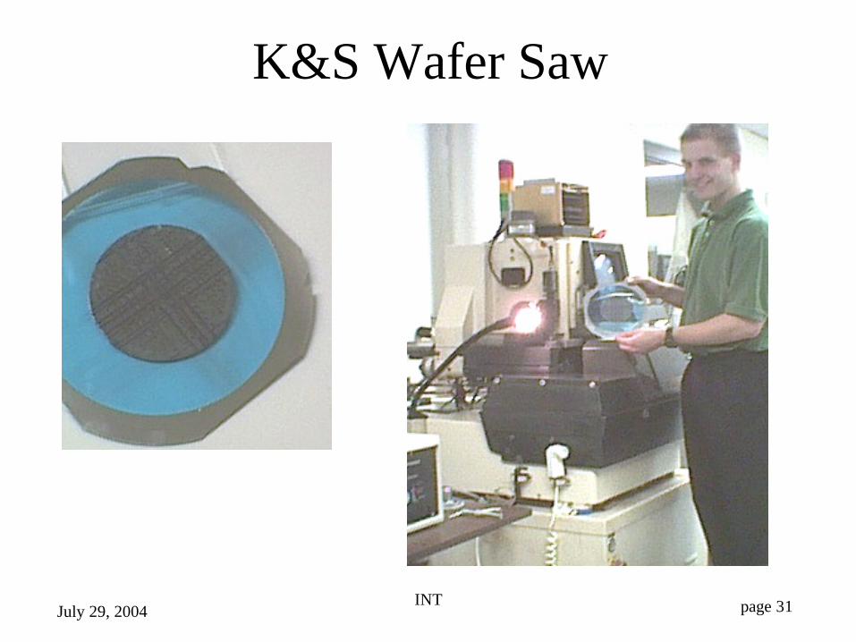
K&S Wafer Saw

INT page 32July 29, 2004
Probe Design
Bacillus subtilis5-7 kb fragment
Probe Name Probe Sequences
ComP AAG CCC TGA CTC TCT CCT TAA TGC CAA A – hexamethyl thiol
yuxH TAC ACG TTC TCT TCG CTT TCT CTA TAA – hexamethyl thiol
Many different probes can test for different DNA molecule fragments of the same bacteria or virus. These probes are purchased from commercial sources.
So with a microchip with 8 sensors we could do 8 different tests for one bacteria or we could repeat one test 8 times for one bacteria or we could do one test each for 8 different bacteria or virus
INT page 33July 29, 2004
GT
G
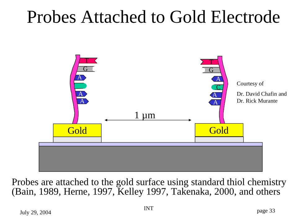
Probes Attached to Gold Electrode
AC
AA
T
AC
AA
Gold Gold
Probes are attached to the gold surface using standard thiol chemistry (Bain, 1989, Herne, 1997, Kelley 1997, Takenaka, 2000, and others
1 µm
Courtesy of
Dr. David Chafin and Dr. Rick Murante
INT page 34July 29, 2004
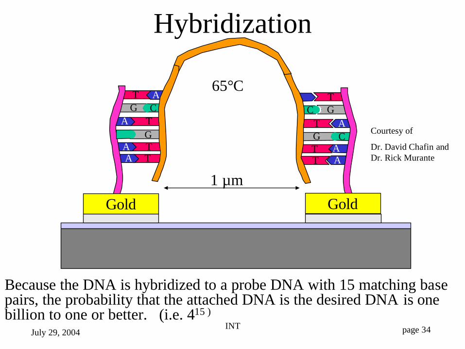
Hybridization
GT
GA
G
AC
T
TT
G
CT
TT
AC
AA
T
AC
AA
Gold Gold
Because the DNA is hybridized to a probe DNA with 15 matching base pairs, the probability that the attached DNA is the desired DNA is one billion to one or better. (i.e. 415 )
1 µm
Courtesy of
Dr. David Chafin and Dr. Rick Murante
65°C
INT page 35July 29, 2004
Verification of Hybridization
A DNA Molecule is only ~2 nm in diameter or 0.002 µmit can not be seen with an optical microscope or with any Scanning Electron Microscope (SEM)
Radioactive Labeled DNA(we could measure the difference betweencomplementary and non-complementary DNA)
Fluorescent Labeled DNA and Fluorescence Microscopy(we could see the Fluorescence from DNAattached to the probes)

INT page 36July 29, 2004
Radioactive DNA Test Results
Complementary vs Non-complementary DNA
020000400006000080000
100000120000140000160000180000
N-comp Comp
Series1
Series2
Rad
ioac
tive
Cou
nts
Microchips presented with complementary DNA showedhigher radioactive counts than non-complementary DNA.

INT page 37July 29, 2004
Still Photographs of Fluorescent Labeled DNA
Electrode 2µm)
Insulator 1µm)
YOYO-1 stainedDNA bridge
YOYO-1 stained DNA bridges
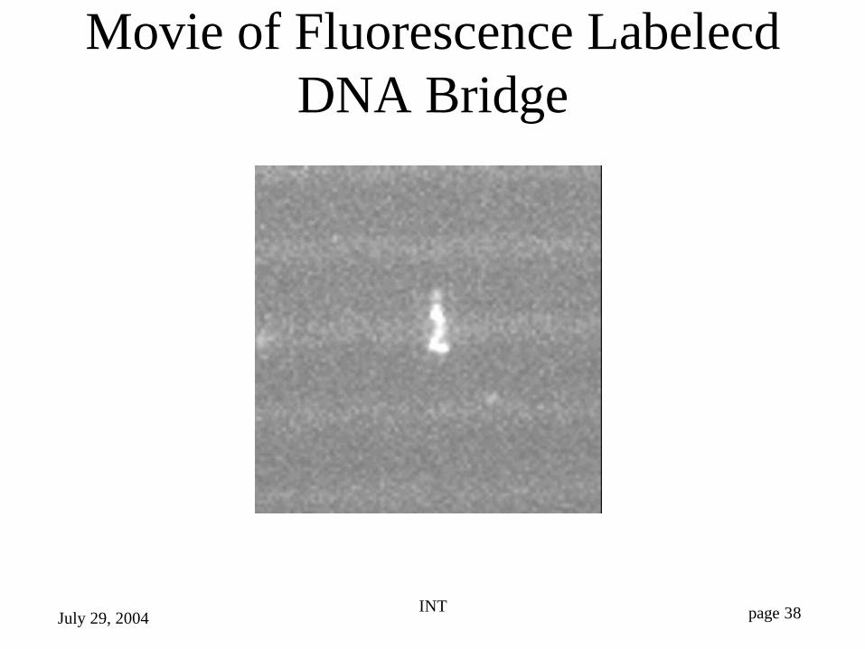
INT page 38July 29, 2004
Movie of Fluorescence LabelecdDNA Bridge

INT page 39July 29, 2004
GT
GA
G
AC
T
TT
G
CT
TT
AC
AA
T
AC
AA
Gold Gold
Ω
Courtesy of Dr. Charlie De Boer
Coating of DNA Bridge with Metal
Braun, 1998Keren, 2002
INT page 40July 29, 2004
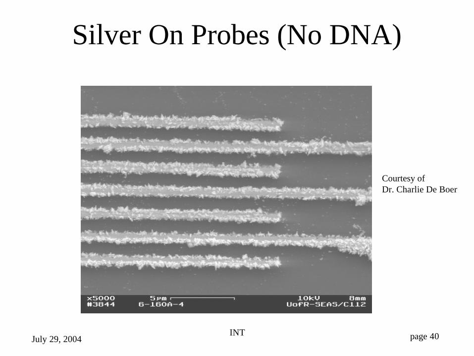
Silver On Probes (No DNA)
Courtesy of Dr. Charlie De Boer

INT page 41July 29, 2004
Silver-Coated DNA
The picture above shows two metal lines 1 micrometer apart with many DNA bridges coated with metal. The measured electrical resistance between the metal conductors dropped from infinity to ~1 thousand ohms, making electrical readout of the detection of a DNA very simple.
Courtesy of Dr. Charlie De Boer
INT page 42July 29, 2004
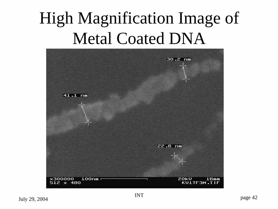
High Magnification Image of Metal Coated DNA
INT page 43July 29, 2004
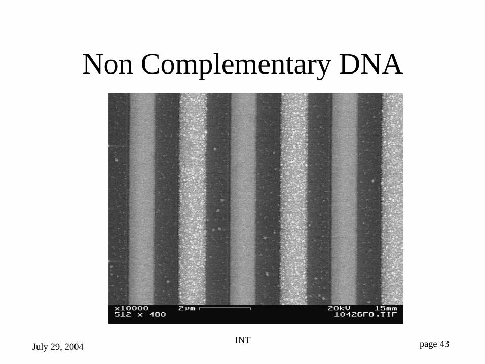
Non Complementary DNA
INT page 44July 29, 2004
Measuring the Resistance of the Metal Coated DNA Bridge
Problem: The metal coated DNA bridge is very fragile and can not be measure reliably with an ohm meter. The sensors are wet and false shorts can be created (electromigration) by applying a few volts for a short time (few seconds).
A custom computer controlled (Lab View) measurement system was created to measure with the lowest possible voltage and complete the measurement in a short time (few msec)
INT page 45July 29, 2004
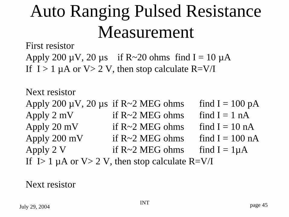
Auto Ranging Pulsed Resistance Measurement
First resistorApply 200 µV, 20 µs if R~20 ohms find I = 10 µAIf I > 1 µA or V> 2 V, then stop calculate R=V/I
Next resistorApply 200 µV, 20 µs if R~2 MEG ohms find I = 100 pAApply 2 mV if R~2 MEG ohms find I = 1 nAApply 20 mV if R~2 MEG ohms find I = 10 nAApply 200 mV if R~2 MEG ohms find I = 100 nAApply 2 V if R~2 MEG ohms find I = 1µAIf I> 1 µA or V> 2 V, then stop calculate R=V/I
Next resistor
INT page 46July 29, 2004
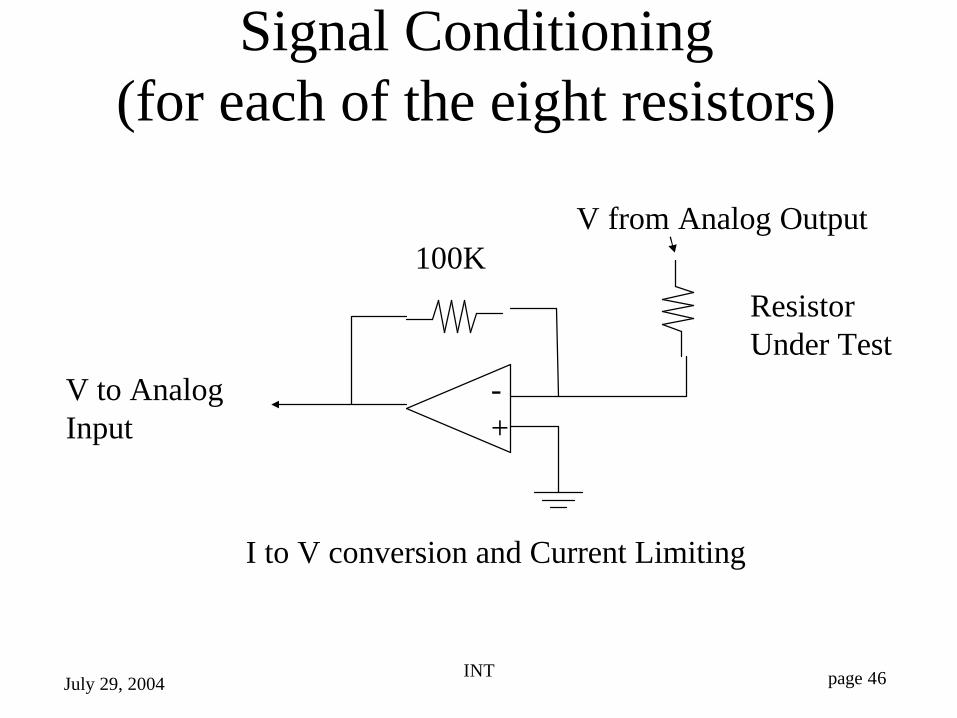
Signal Conditioning(for each of the eight resistors)
-+
Resistor Under Test
I to V conversion and Current Limiting
100K
V to AnalogInput
V from Analog Output
INT page 47July 29, 2004
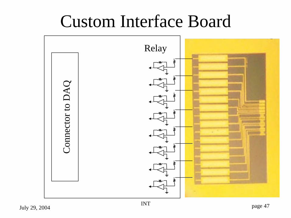
Custom Interface BoardRelay
Con
nect
or to
DA
Q
INT page 48July 29, 2004
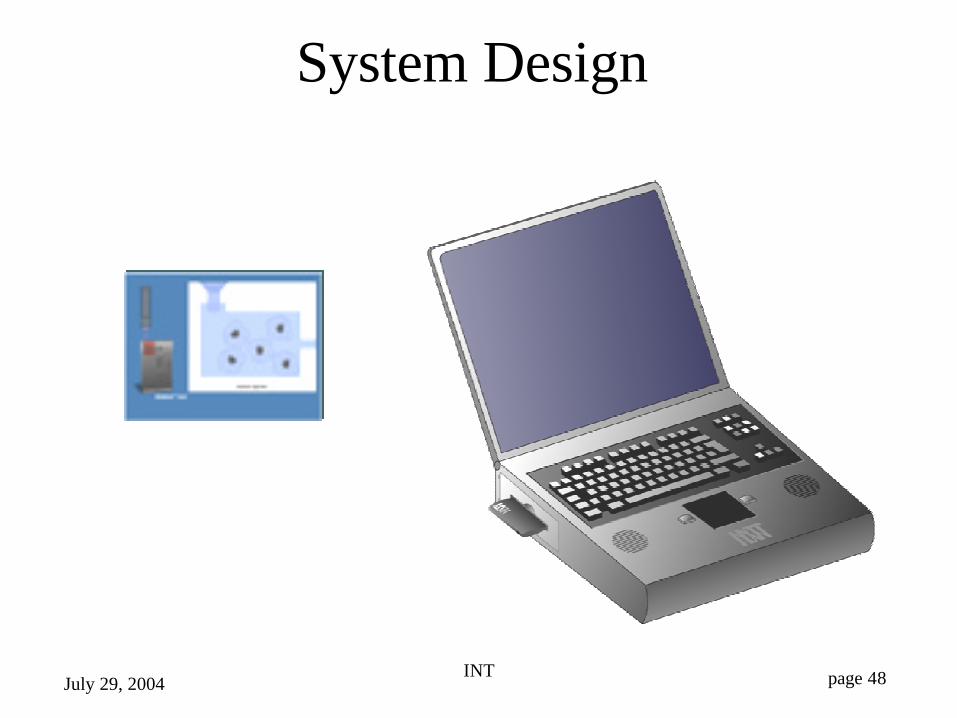
System Design

INT page 49July 29, 2004
INT Bio-Detect Card
INT page 50July 29, 2004
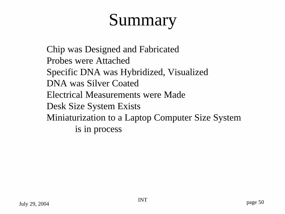
Summary
Chip was Designed and FabricatedProbes were AttachedSpecific DNA was Hybridized, VisualizedDNA was Silver CoatedElectrical Measurements were MadeDesk Size System Exists Miniaturization to a Laptop Computer Size System
is in process

INT page 51July 29, 2004
AcknowledgementsSpecial thanks to:
Integrated Nano-Technologies, Employees (Some are listed below)
•Dr. Michael Connolly, President and CEO
•Dr. Charlie De Boer, Senior Research Scientist
•Dr. David Chafin, Director, R & D
•Dr. Rick Murante, Research Scientist
•Dr. Samina Jafri, Research Scientist
•Ms. Roberta Greco, Chemist
•Mr. Scott Seabridge, Electrical Engineer
INT page 52July 29, 2004
INT page 53July 29, 2004
INT page 54July 29, 2004
![Optimization of silicon detector layout and associated front-end ... · for a given electrode and doped implant arrangement. Next, a charge propagation model [4] using TCAD calculated](https://img.pdfslide.net/doc/110x75/5e409cb2bd2b6a18bd52b810/optimization-of-silicon-detector-layout-and-associated-front-end-for-a-given.jpg)