Embed Size (px)
Citation preview

An Introduction to FPGAsAli Abbasi, Dr. Saeed Reza Khammar
Department of Computer Engineering, University of Sistan and Baluchestan, Iran

Chapter 4: Introduction to FPGAs
▪ FPGA Structure
▪ CLB Structure
▪ Application Specific Blocks in FPGA
▪ FPLD Programming Technologies
▪ FPGA Market and Examples
▪ Design Flow
4-2/32

FPGA Structure
• Configurable Logic Blocks:
Also known as Logic Block(CB),
Logic Cell(LC),...
Programmable blocks to perform
logic functions
• Switch Matrix:
Programmable switches to establish
connection between CLBs and I/O
Blocks.
• Input/Output Blocks:
An interface for external connections
to FPGA
4-3/32

CLB Structure
• Each CLB is a PLD-like block.
• Plus some usefull elements like Flip-Flops.
• CLB architecture and design of each FPGA is exclusive (see data-sheets for
more information about blocks).
• They commonly use SoP-based, LUTs, or multiplexers for programmable
logic implementation *.
4-4/32* See Chapter 3, Programmable Logic Basis.

Application Specific Blocks in FPGAs
• There are some pre-manufactured full-custom blocks instead of CLBs.
• These blocks are designed to perform an specific task.
• Examples: Memory Blocks, Processor Blocks, Arithmetic Blocks, Clock
Management Blocks, Gigabit Transceiver Blocks
4-5/32

Memory Blocks
• There are two types of memory in FPGAs:
– Blocked Memory
– Distributed Memory
• Blocked memories are desgined full-custom in companies and are ready to
be used by designers.
• Also, designers can use CLBs for implementing a memory (not sufficient
enough, but useful) which is called a distibuted memory.
4-6/32

Processor Blocks
• A specific block to implement an Instruction Set Architecture (ISA) beside usual
digital designs.
• FPGA manufacturers define the instruction set.
• Each company has its own ISA (e.g. Microblaze for Xilinx, Nios II for Intel).
• Despite these hard processor cores, designers can implement their own processor
using CLBs (also known as a soft processor).
4-7/32

Arithmetic Blocks
• Implementing multipliers using CLBs
needs a lot of recources and it will have a
slow operation. Therefore, hard design of
these blocks in FPGAs helps designers
with better recource allocation.
• Performing large-sized sum or sub needs
a large carry chain. Routing these carries
using SBs will remarkably reduces the
performance, so there are some direct
connections between adjacent CLBs.
• The main use of these blocks is in digital
signal processing (DSP) that needs a lot
of arithmetic operations.
4-8/32
Clock Management Blocks
• Clock problems acccure due to noise or weakening over distance.
– Clock Skew
– Jitter
4-9/32
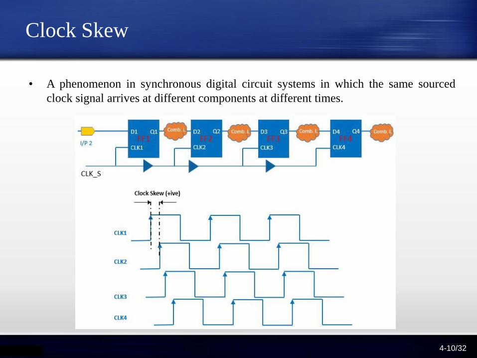
Clock Skew
• A phenomenon in synchronous digital circuit systems in which the same sourced
clock signal arrives at different components at different times.
4-10/32

Jitter
• Deviation from true periodicity of a presumably periodic signal (e.g. clock signal)
4-11/32

Clock Management Blocks (cont.)
• Clock problems acccure due to noise or weakening over distance.
– Clock Skew
– Jitter
• Clock management block overcomes clock skew by monitoring signals with skew (as
feedback) and changing the phase of the source clock until the skew fades.
• Also, it solves the jitter problem.
4-12/32

Clock Management Blocks (cont.)
• Since FPGAs recieve only one clock from external sources (e.g. an oscillator), one of
the other important functions of a clock management block is to generate clock
signals with different frequencies from the source clock (designers control the
frequency ratio and phase difference).
Picture Source: Computer-Aided Digital Systems Design, Dr Morteza Seheb Zamani, page 125, with modifications
Input Clock
Clock
Management
Block
4-13/32

Gigabit Transceiver Blocks
• Can be considered as an I/O block.
• But supports high-speed data transmission (~Gbps)
• Transmits bits in serial (one bit per cycle – single-ended or differential)
4-14/32Further Reading: Data Communications and Networking, Dr. Forouzan

Gigabit Transceiver Blocks (cont.)
• Much better than parallel data communication (e.g. use of 64 I/O pins for 64
bits of data?)
• What about electromagnetic effect on these 64 wires
• Synchronization of these 64 connections with one clock is much challenging
4-15/32

Single-ended vs Differential
• Both refer to the reference for a voltage
• Single-ended is referred to ground while differential is referred to some other
voltage
4-16/32
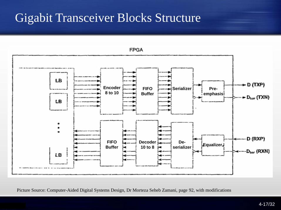
Gigabit Transceiver Blocks Structure
Encoder
8 to 10
Decoder
10 to 8
SerializerFIFO
Buffer
Pre-
emphasis
EqualizerDe-
serializer
FIFO
Buffer
Picture Source: Computer-Aided Digital Systems Design, Dr Morteza Seheb Zamani, page 92, with modifications
4-17/32

Data Encoder
Picture Source: Computer-Aided Digital Systems Design, Dr Morteza Seheb Zamani, page 94, with modifications
• Several continuous ‘0’s or ‘1’s will
disturb direct current (DC) balance
after serialization
• In an 8 to 10 data encoder, series of
bits will be encoded in a way that
there are no 5 continuous ‘0’s or ‘1’s
in the final sequence
• Scrambling is another method for
increasing the number of states and
error reduction
4-18/32

Pre-emphasis
Picture Source: Computer-Aided Digital Systems Design, Dr Morteza Seheb Zamani, page 100
4-19/32

FPLD Programming Technologies
• FPLDs use one of the following technologies for programming:
– SRAM
– Flash
– EEPROM
– Anti-fuse
4-20/32

SRAM
Advantages:
– Unlimited times of programming
– Chip is tested by manufacturer
– Runtime programming
Disadvantages:
– Volatile
– High area
– Low security
4-21/32

Flash and EEPROM
Advantages:
– Non volatile
– Low area
– High security (due to floating gate tansistors)
Disadvantages:
– High cost of manufacturing (due to FGTs)
– Slower programming compared to SRAM
Flashes and EEPROMs are completely similar; however, in
flashes, data is removed in blocks, whereas in EEPROMs it
is removed in words.
4-22/32

Anit-fuse
Advantages:
– Non volatile
– Low area
– High security (surgery required for stealing!)
– Low power
Disadvantages:
– Not reprogrammable
4-23/32
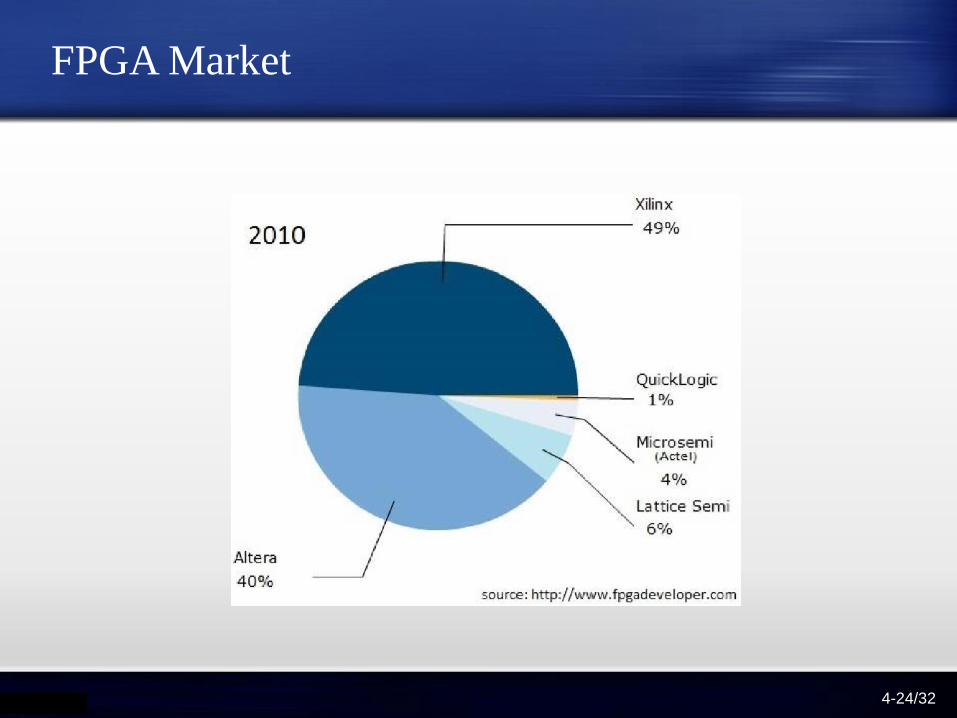
FPGA Market
4-24/32

FPGA Examples: Xilinx Spartan-II
4-25/32

FPGA Examples: Xilinx Virtex-II
4-26/32

FPGA Examples: Xilinx Virtex-IV
4-27/32

FPGA Examples: Altera Cyclone V
4-28/32

Design Flow
4-29/32

Physical Design
Picture Source: CEIT483 at Amirkabir U. ofTech., Lecture 2, by Dr Saheb-zamani, with modifications
4-30/32

Further Reading
[1] Computer-Aided Digital Systems Design, Dr Morteza Seheb Zamani
Chapter 1 - 3
4-31/32

Any Question?
4-32/32


![Chapter 2 FPGA Architectures: An Overview · 2015. 8. 12. · 2.1 Introduction to FPGAs FieldprogrammableGateArrays(FPGAs) ... ofmultiplexors[44],lookuptable(LUT)[121]andPALstylewideinputgates[124]](https://img.pdfslide.net/doc/110x75/61161dad44825b61eb07947d/chapter-2-fpga-architectures-an-overview-2015-8-12-21-introduction-to-fpgas.jpg)