Embed Size (px)
Citation preview

Philips tech. Rev. 35, 199-208, 1975, No. 7/8
An investigation of ion etching
H. Dimigen and H. Lüthje
The ever-increasing demand for furtherminiaturization continues to result in thedevelopment of new processes. The articlebelow describes a method of etching basedon the use of accelerated inert-gas ions,which is already in use in many laboratoriesand in pilot production. Compared with thechemical etching methods that have nor-mally been used until now, this method im-proves the resolution in a lateral directionby a full order of magnitude for the sameetch depth, or gives a considerably greateretch depth for the same lateral resolution.The method has previously been mainlyemployed in semiconductor technology, butits value has also been demonstrared in awide range of'other applications.
199
Introduetion
Etching is an important step III the semiconductortechnology for the man ufacture of integrated cir-cuits [11. Chips of semiconductor material, usually sili-con, are first oxide-coated by means of heat treatmentand openings are etched in the oxide layer. Diffusionsthrough these openings form zones of the appropriateP: or N-type silicon at the desired locations. In the pastthe etching has usually been done with reagents suchas hydrogen fluoride (chemical etching methods) al-though recently other methods have gained ground.
One of these recent methods, ion etching, is the sub-ject of this article. The increased attention that thismethod has attracted in recent years is connected withthe increasingly exacting requirements that progressiveminiaturization places on etching technology-require-ments that can no longer be met by the conventionalchemical etching methods. These chemical methodswill only give a smallest separation of about 5 [Lmbetween adjacent grooves of an etched pattern with adesired etch depth of about 1 [Lm. With ion etching,
Dr H. Dimigen and H. Liithje are with Philips Forschungslabora-toriurn Hamburg Gmb H, Hamburg, West Germany.
however, patterns can be made under the same condi-tions with groove spacings of only I [Lm.
Ion etching consists in bombarding the surface of thesubstrate with ions of an inert gas (sputtering) whichcauses an erosion of the surface layer. This erosion is adirect result of the collision process, i.e. the physicalinteraction between the incident ions and the surface ofthe substrate. In this article we shall not consider thechemical attack on surfaces by certain reactive ionssometimes used in methods such as plasma etching.
Ion etching is useful in many other fields besidessemiconductor technology. Its applications include theproduction of spiral-groove bearings and of integratedoptics, and also the fabrication of the patterns used inbubble and magneto-optical memories. The title photo-graph shows an example of its use in a magneto-opticalmemory. The pattern shown has a periodicity of 20 [Lm,while the grooves between the individual elements are10 [Lmwide and 5.5 [Lm deep [21.
[1] See for example A. Schmitz, Philips tech. Rev. 27, 192, 1966.[2] J.-P. Krumme and H. Dimigen, IEEE Trans. MAG-9, 405,
1973.

200 H. DIMIGEN and H. LÜTHJE Philips tech. Rev. 35, No. 7/8
Ion-etching methods now in use
The ions most commonly used for etching the sur-faces of solids are those of argon, at an energy between500 and 5000 eV, most of which is converted into heat
Fig. 1. The type of specimen on which most of the investigations in the su bstrate. The heat flux that the su bstrate willdescribed were carried out: a silicon chip covered with a thincoating of oxide, with an etching mask consisting of parallel withstand is therefore the quantity that determines thestrips of titanium or other substance on top of it. After ion etch- maximum permissible energy density of the ions. It ising, the specimen is broken al right angles to the longitudinaldirection of the strips and the resultant cross-section is compared generally in the region of several watts per square centi-under a microscope with that of the unetched specimen. metre.
In the course of our investigation reported here intoion etching we made frequent use of specimens of thetype illustrated in fig. J. These consist of a silicon chipof diameter of about 30 mm, covered in some cases bya thin oxide layer, to which an etching mask that mighttypically be a titanium pattern of parallel strips 20 [Lm
wide and 1-2 urn thick has been applied. The effect ofion bombardment on these specimens is easily investi-gated by breaking them at right angles to the stripsafter etching and studying the exposed cross-sectionunder a microscope.
Fig. 2 shows such a cross-section before and afteretching (a titanium mask on a silicon substrate). Weconclude from our examination of this cross-sectionthat there has been etching of both the mask and thesubstrate, so that the original pattern of both the sub-strate surface and the mask have been altered by theetching.It is understandable that both should have been
affected, since the bombardment energy required toensure a sufficiently high etch rate is several orders ofmagnitude greater than the bond energy of atoms inthe solid state. There are therefore no solids that wouldbe unaffected by such a bombardment.
The extent to which the resultant etched pattern dif-fers from the original mask pattern is the main thingthat determines the practibility of ion etching as a
production method. In the last few years we have con-ducted extensive investigations with the aim of deter-mining the effect of various parameters on the resultof etching, in order to make the process as suitable aspossible for practical use.
Our investigations showed that it is not necessary atthe outset to consider in detail the mechanism of themicroscopie collision processes that occur between theetching ion and the surface of the substrate [3]; it issufficient to know the average value of the sputteringrate S (the number of ions sputtered per incident ion)that each material exhibits on bombardment with ionspossessing a well defined energy.
We shall now begin by giving a description of twoion-etching methods now in use. This will be followedby a section dealing with the etch rates that can beattained. Finally, we shall analyse the changes pro-duced in the mask and substrate by the etching, fromwhich we shall draw a number of conclusions relatingto the requirements placed upon the mask material.
Fig. 2. Cross-section of a silicon chip with titanium strips, (a) be-fore and (b) after etching. It can be seen that the mask as wellas the substrate has been attacked by the etching.
Philips tech. Rev. 35, No. 7/8 ION ETCHING 201
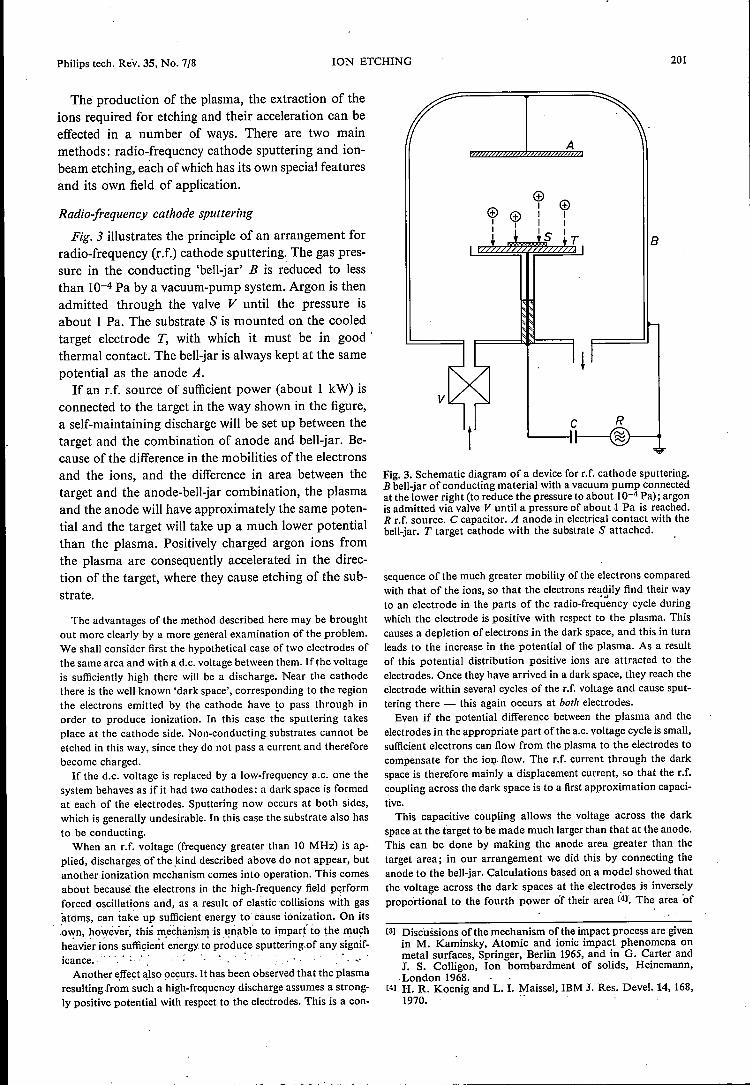
The production of the plasma, the extraction of theions required for etching and their acceleration can beeffected in a number of ways. There are two mainmethods: radio-frequency cathode sputtering and ion-beam etching, each ofwhich has its own special featuresand its own field of application.
Radio-frequency cathode sputtering
Fig. 3 illustrates the principle of an arrangement forradio-frequency (r.f.) cathode sputtering. The gas pres-sure in the conducting 'bell-jar' B is reduced to lessthan 10-4 Pa by a vacuum-pump system. Argon is thenadmitted through the valve V until the pressure isabout 1 Pa. The substrate S is mounted on the cooledtarget electrode T, with which it must be in good'thermal contact. The bell-jar is always kept at the samepotential as the anode A.
If an r.f. source of sufficient power (about 1 kW) isconnected to the target in the way shown in the figure,a self-maintaining discharge will be set up between thetarget and the combination of anode and bell-jar. Be-cause ofthe difference in the mobilities ofthe electronsand the ions, and the difference in area between thetarget and the anode-bell-jar combination, the plasmaand the anode will have approximately the same poten-tial and the target will take up a much lower potentialthan the plasma. Positively charged argon ions fromthe plasma are consequently accelerated in the direc-tion of the target, where they cause etching of the sub-strate.
The advantages of the method described here may be broughtout more clearly by a more general examination of the problem.We shall consider first the hypothetical case of two electrodes ofthe same area and with a d.c. voltage between them. Ifthe voltageis sufficiently high there will be a discharge. Near the cathodethere is the well known 'dark space', corresponding to the regionthe electrons emitted by the cathode have ~o pass through inorder to produce ionization. In this case the sputtering takesplace at the cathode side. Non-conducting substrates cannot beetched in this way, since they do not pass a current and thereforebecome charged.
If the d.c. voltage is replaced by a low-frequency a.c. one thesystem behaves as if it had two cathodes: a dark space is formedat each of the electrodes. Sputtering now occurs at both sides,which is generally undesirable. In this case the substrate also hasto be conducting.
When an r.f. voltage (frequency greater than 10 MHz) is ap-plied, discharges. of the kind described above do not appear, butanother ionization mechanism comes into operation. This comesabout because the electrons in the high-frequency field performforced oscillations and, as a result of elastic 'collisions with gasatoms, can take up sufficient energy to cause ionizátion. On its"own, however; this mechanism is unable to impart to the much. ,,- .. _- ." _ .. ' - -, -.' .heavier ions sufficient energy ,to produ~e sputtering. of any ~ignif-icance ..
Another effect also occurs. It has been observed that the plasmaresultingfrom such a high-frequency discharge assumes a strong-ly positive potential with respect to the electrodes. This is a con-
A
8
v
Fig. 3. Schematic diagram of a device for r.f. cathode sputtering.B bell-jar of conducting material with a vacuum pump connectedat the lower right (to reduce the pressure to about 10-4 Pa); argonis admitted via valve V until a pressure of aboutl Pa is reached.R r.f. source. C capacitor. A anode in electrical contact with thebell-jar. T target cathode with the substrate S attached.
sequence of the much greater mobility of the electrons comparedwith that of the ions, so that the electrons readily find their wayto an electrode in the parts of the radio-frequency cycle duringwhich the electrode is positive with respect to the plasma. Thiscauses a depletion of electrons in the dark space, and this in turnleads to the increase in the potentialof the plasma. As a resultof this potential distribution positive ions are attracted to theelectrodes. Once they have arrived in a dark space, they reach theelectrode within several cycles of the r.f, voltage and cause sput-tering there - this again occurs at both electrodes.Even if the potential difference between the plasma and the
electrodes in the appropriate part of the a.c. voltage cycle is small,sufficient electrons can flow from the plasma to the electrodes tocompensate for the ion. flow. The r.f. current through the darkspace is therefore mainly a displacement current, so that the r.f.coupling across the dark space is to a first approximation capaci-tive.This capacitive coupling allows the voltage across the dark
space at the target to be made much larger than that at the anode.This can be done by making the anode area greater than thetarget area; in our arrangement we did this by connecting theanode to the bell-jar. Calculations based on a model showed thatthe voltage across the dark spaces at the electrodes is inverselyproportional to the fourth power of their area [41.The area of
[3] Discussions of the mechanism of the impact process are givenin M. Kaminsky, Atomic and ionic impact phenomena onmetal surfaces, Springer, Berlin 1965, and in G. Carter andJ. S. Colligon, Ion bombardment of solids, Heinemann,-London 1968.
[4] H. R. Koenig and L. I.Maissel, IBM J. Res. DeveI. 14, 168,1970. .,

202 H. DIMIGEN and H. ,LÜTHJE Philips tech. Rev. 35, No. 7/8
the electrode formed by the anode and bell-jar need not there-fore be much larger than that of the target in order to reducethe voltage across the dark space at the anode to practically zeroand ensure a high voltage across the dark space at the target,so that the ions accelerated in the direction of the target acquirethe energy required for sputtering, while no sputtering occurs atthe anode.It will also be necessary to compensate the voltage across the
dark space at the target by a d.c. voltage somewhere between thetarget and the voltage source. One way of doing this is to includea capacitor in the external part of the circuit (see fig. 3), or to usea non-conducting substrate for the target. This means that a non-conducting substrate is not now merely permissible, it is advan-tageous.
There are two particularly interesting aspects of r.f.cathode sputtering: the equipment required foretchingis very simple, and it is possible to use very large targets(with diameters of 30 cm or more), so that many sub-strates can be etched simultaneously. This is extremelyimportant in production applications. As we have seen,the method is also suitable for etching non-conductingsubstrates, while the use of an a.c. voltage prevents thecharging of the substrate that would otherwise resultfrom the ion bombardment, since the charge is can-celled by a periodic supply of electrons.There is however the disadvantage that, as a result
of the potential distribution around the target, theetching ions can only strike the target and substrate atright angles to the surface. This makes it impossible tocarry out ion etching at any other angle of incidence.Another disadvantage is that a gas discharge of the
type used here requires a relatively high argon pressure,since the mean free path of the ions has to be appre-ciably smaller than the distance between the target andthe anode. As we shall show later, this can have a veryadverse effect on the results of etching.
Ion-beam etching
The second etching method we wish to discuss- etching with an ion beam - can be carried out withan arrangement of the kind shown schematically infig· 4. An are discharge is set up in the upper part ofthe bell-jar B, which contains argon, with the aid of aheated cathode Ca and an anode A. The gas pressurein an are discharge can be very low; in this case it isabout 10-2 Pa. Ions are drawn away from the are by asieve-like electrode E, then accelerated and fired intothe lower part ofthe bell-jar. The current density oftheion beam is increased by a magnetic field produced bythe coil Co. The ions thus released finally strike thesubstrate S, mounted on a cooled substrate holder SH,which can be rotated about two axes.This arrangement has a number of advantages. The
energy .and current density of the ions can be variedindependently, since the are discharge, the voltage on
the electrode E and the strength of the magnetic fieldcan all be adjusted separately. Since the region aroundthe substrate is nearly free of field, the substrate can bebombarded at any desired angle. The gas pressure canbe kept so low that the mean free path of the ions islarge with respect to the distance between the substrateand the bell-jar. J
As in r.f. cathode sputtering, it is possible to etchdielectrics, provided that the positive surface chargecreated in the process is compensated by a source ofelectrons.These beneficial features are to some extent offset by
disadvantages. The system is relatively expensive, whilethere is at present no device that can deliver a sufficient-ly homogeneous and dense beam with a diameter muchgreater than 8 cm. Simultaneous etching of a largenumber of substrates with a large area is therefore notpossible.
Etch rate
Anyone interested in ion etching will obviously wishto know what kind of etch rates can be achieved, i.e. thelayer depth removed per unit time. The etch rate de-pends on many parameters, such as the kind of ion, theenergy and density of the ions, and the nature of the
+50V =
~ ICa Et) r
C ~ Ep! Et) A ~C
0r;:I6J===:J-:t__t_ _t_===~=::;-] 0E
So
Et)IIIII
s~ B
Fig. 4. Schematic diagram of an arrangement for ion-beam etch-ing. Ions are removed from an arc discharge between the filament-ary cathode Ca and the anode A by means of the sieve-like elec-trode E and the coil Co, accelerated and fired into the lower com-partment of the bell-jar B. The ion beam produced strikes thesubstrate S, located on the substrate holder SH, which can rotateabout two axes. A pump is connected to the lower aperture, andargon is admitted via the upper aperture. In this arrangement thepressure can be lower (about 10-2 Pa) than in the device describedin fig. 3. So electron source used to compensate for any surfacecharge produced on the substrate.
Philips tech. Rev. 35, No. 7/8 ION ETCHING 203
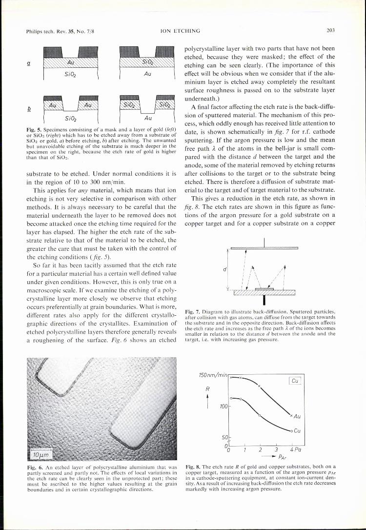
Au
Fig. 5. Specimens consisting of a mask and a layer of gold (left)or Si02 (right) which has to be etched away from a substrate ofSi02 or gold, a) before etching, b) after etching. The unwantedbut unavoidable etching of the substrate is much deeper in thespecimen on the right, because the etch rate of gold is higherthan that of Si02.
substrate to be etched. Under normal conditions it isin the region of 10 to 300 nmjmin.
This applies for any material, which means that ionetching is not very selective in comparison with othermethods. It is always necessary to be careful that thematerial underneath the layer to be removed does notbecome attacked once the etching time required for thelayer has elapsed. The higher the etch rate of the sub-strate relative to that of the material to be etched, thegreater the care that must be taken with the control ofthe etching conditions (fig. 5).
So far it has been tacitly assumed that the etch ratefor a particular material has a certain well defined valueunder given conditions. However, this is only true on amacroscopie scale. If we examine the etching of a poly-crystalline layer more closely we observe that etchingoccurs preferentially at grain boundaries. What is more,different rates also apply for the different crystallo-graphic directions of the crystallites. Examination ofetched polycrystalline layers therefore generally revealsa roughening of the surface. Fig. 6 shows an etched
Fig. 6. An etched layer of polycrystalline aluminium that waspartly screened and partly not. The effects of local variations inthe etch rate can be clearly seen in the unprotected part; thesemust be ascribed to the higher values resulting at the grainboundaries and in certain crystallographic directions.
polycrystalline layer with two parts that have not beenetched, because they were masked; the effect of theetching can be seen clearly. (The importance of thiseffect will be obvious when we consider that if the alu-minium layer is etched away completely the resultantsurface roughness is passed on to the substrate layerunderneath.)
A final factor affecting the etch rate is the back-diffu-sion of sputtered material. The mechanism of this pro-cess, which oddly enough has received little attention todate, is shown schematically in fig. 7 for r.f. cathodesputtering. If the argon pressure is low and the meanfree path ). of the atoms in the bell-jar is small com-pared with the distance d between the target and theanode, some of the material removed by etching returnsafter collisions to the target or to the substrate beingetched. There is therefore a diffusion of substrate mat-erial to the target and of target material to the substrate.
This gives a reduction in the etch rate, as shown injig. 8. The etch rates are shown in this figure as func-tions of the argon pressure for a gold substrate on acopper target and for a copper substrate on a copper
Fig. 7. Diagram to illustrate back-diffusion. Sputtered particles,after collision with gas atoms, can diffuse from the target towardsthe substrate and in the opposite direction. Back-diffusion affectsthe etch rate and increases as the free path it of the ions becomessmaller in relation to the distance d between the anode and thetarget, i.e. with increasing gas pressure.
7S0nm/minr_--------------,x~ ~
IIOD~'~0, xAu
"'-.oCu
2 4. Pa3
Fig. 8. The etch rate R of gold and copper substrates, both on acopper target, measured as a function of the argon pressure PArin a cathode-sputtering equipment, at constant ion-current den-sity. As a result of increasing back-diffusion the etch rate decreasesmarkedly with increasing argon pressure.

204 H. DIMIGEN and H. LÜTHJE
target. It can be seen that both rates decrease in aboutthe same proportion with increasing argon pressure,i.e. with increasing back-diffusion. ln this case it ap-parently makes no difference whether the atoms back-diffused are of a different material (copper on gold) orof the same material (copper on copper).
Another complication that can arise with back-diffu-sion is that the back-diffused target material can adhereto the substrate surface in such a way that the etch rateis lowered more by this material in its new environmentthan might be expected from the results shown infig. 8 [5]. A case of this kind is illustrated in fig. 9.Titanium targets with substrates of either titanium orsilicon were used for the experiments. It was found that
1
Philips tech. Rev. 35, No. 7j8
BOnm/minr-------------,
R
t60
t
- PAr
Fig. 9. As fig. 8 but with titanium and silicon substrates on atitanium target. ln this case we find that as a result of back-diffu-sion titanium deposited in a silicon environment produces agreater reduction of the etch rate than when it is deposited in atitanium environment. It would appear that some kind of bondis formed between titanium and silicon.
10pm
d/'A=4.8
Fig. 10. The effect of an ion bombardment on a silicon substrate coated with a titanium mask(strips 20 [.I.mwide, 3 [.1.111 in thickness). Etch time t increases from top to bottom, while theargon pressure, and hence the ratio djJ.. (see fig. 7), increases from left to right. With increasingetch time the width of the strips becomes smaller and the slope at the edges decreases. 'Ditches'also appear on either side of the strips; the ditches increase in depth and width with increasingback-diffusion.
with negligibly small back-diffusion the etch rate of thesilicon is higher than that for titanium; however, theconverse situation comes into effect as the back-diffu-sion increases. It appears that titanium has an appreci-ably lower etch rate in the presence of silicon than onits own.
The solution to many etching problems can be con-siderably complicated by the effect of back-diffusion.Surfaces that have to be cleaned by ion etching are infact contaminated by back-diffusion, which again isundoubtably responsible for many of the uncertaintiesencountered in comparisons of the etch rates, or ratios

Philips tech. Rev. 35, No: 7/8 ION ETCHING 205
of the etch rates, reported by many investigators. Thesituation will be clarified when back-diffusion is suffi-ciently taken into account in ion-etching experiments.
The imaging of the mask in the substrate
The quality of an etching method used to apply a pat-tern depends on the accuracy with which the mask pat-tern originally applied is reproduced in the layer to beetched. In fig. 2 it could be seen that this is a problemin ion etching, because under ion bombardment thedimensional stability of the mask is never perfect. Weshall now take a closer look at this problem.Fig. la shows some of the stages in the ion-etching
process. The picture right at the top shows a cross-section of a substrate (Si) as yet unetched and with amask on top of it (a titanium strip 20 [Lmwide andabout 3 [Lmthick). Other cross-sections are arrangedbeneath this first one in order of increasing etch time,for three different values of the gas pressure and henceof the ratio djA. The following points emerge imme-diately. The mask strip becomes narrower and narrow-er during etching and the slope of the sides of the stripalso changes. 'These effects depend on the ratio djA,but also arise when the back-diffusion of the sputteredmaterial is negligible (d/A < 1).The changes undergone by the mask strip are to a
large extent determined by the way in which the etchrate depends on the angle of incidence of the ions onthe substrate. Fig. 11shows how most materials behavein this respect. The quantity Sce), i.e. the number ofsputtered particles per ion incident at the surface, goesto a maximum and then decreases rapidly (fig. IIa).The significanee of this for the shape of the mask stripduring etching is illustrated in fig. lIb. In addition toa change in slope angle, there is also a marked narrow-ing of the mask strip, because the sides are etched awayfaster than the top.The way in which the width reduction b.L depends
on S(e) and the etch depth b.d [6] is given by:
~s(e) ~b.L = b.d - - I (tan e)-I.S(O)
The results of measurements that we made confirm thisrelation; they are shown in Table J. The inconsistenciesthat we found in these measurements when etchinglayers of titanium and molybdenum are associated withthe peculiar anisotropic structure of these layers.The explanation for the 'ditches' seen in the etched
material near the edges of the mask strip in fig. 10 isprobably a locally higher etch rate due to ions rebound-ing elastically from the sides. These ditches are narrowwhen the back-diffusion is negligible, but become ap-preciably wider and deeper with increasing back-diffu-
Table J. The ratio of the width reduction t;..L of the mask stripin fig. 1, occurring as a result ofion etching, to the etch depth tsd,and also the ratio S(e)/S(O) (see fig. I la), calculated 'andmeas-ured for six values of the angle of incidence e. '
Material e IlL//:,d S(e)/S(O) S(e)/S(O)(0) measured calculated measured
Silicon (lil) 31 0.98 1.59 1.72Silicon (lIl) 57 2.34 4.60 4.02Si02 35 1.46 2.02 2.25Photoresist
(AZ 1350H) 68.7 1.35 4.46 3.87Titanium 45 0.04 1.04 1.89Molybdenum 60 . 0,04 1.07 1.48
s
t
Q0 "30 ,60 ' 90°
-8
I IJ 1
!Cf I
\ 'tt,..",',.r .c. ~~:.H
,.;;;-.
Q
Fig. 11. a) Example showing how the sputtering rate S(e), i.e.the number of sputtered particles per incident ion, depends onthe angle of incidence e. b) The low value ,of sputteringrate forvertical incidence compared with that obtained with bombard-ment at an angle accounts for the reduction of the width of themask strips during etching. The fact that the top and side 'of themask strip never meet at a sharp corner but merge smoothlymeans that the etch rate is faster at the top of the side surfacethan underneath, resulting in a reduction of the slope duringetching. (The upper figure in (b) is the unetched specimen, thelower figure the etched specimen.)
sion. Fig. 12 gives an explanation for this. Whilepoint A receives back-diffusing material from the solidangle Q)1, point B, which is closer to the side of themask strip, receives material from the much smallersolid angle Q)2. The difference between sputtered andback-diffused material results in a higher etch rate for
[5] M. L. Tarng and G. K. Wehner, J. appl. Phys. 43, 2268,1972.[6] A. D. G. Stewart and M. W. Thompson, J. Mat. Sci. 4, 56,
1969. '

206 H. DIMIGEN and H. LOTHJE Philips tech. Rev. 35, No. 7/8
point E, i.e. in a.deeper ditch. Quantitatively, the situa- .tion is in fact much more complicated because the widthreduction of the mask strip referred to above continu-ously changes the conditions for the formation ofditches during the etching process.
Fig. 12. Digram illustrating the deepening of the 'ditches' formedduring the etching as a result of back-diffusion. The solid anglerJh through which ions back-diffuse to point B is smaller thandh, which is the corresponding solid angle for point A. Thisresults in a higher etch rate at B than at A, and hence in a deeperditch.
Requirements to. be met by the mask
Because of the ditch formation it is often desirable torestrict the back-diffusion of sputtered material to aminimum by proper choice ofthe etching method (usu-ally ion-beam etching). When that condition is ob-served, the accuracy with which the mask pattern isreproduced in the etched pattern depends almost en-tirely on the behaviour of the mask during etching.Itwill also be clear that if it is desired to etch relative-
ly deep with a thin mask, the etch rate of the mask willhave to be low compared with that ofthe material to beetched. The desirability ofusing thin masks arises fromthe fact that only thin masks can be made with highlateral resolution and that therefore only thin maskscan give the high-resolution etch patterns that, as statedearlier, constitute the great attraction of ion etching.The two most important requirements that mask
material must satisfy follow from what has been saidabove. Firstly, its etch rate must be as low as possible.Secondly, sputtering should depend as little as possibleon the angle of incidence of the ions, for only underthat condition can changes in the mask pattern duringetching be kept to a minimum.If we consider mask materials that might be suitable
for the first requirement, the following picture emerges.Photoresist masks give a relatively low etch rate pro-vided the pressure of the residual gas in the bell-jar isvery low (photoresists are usually organic and suscep-tible to attack by reactive residual gases). This condi-tiori can be met either with a good pump system or byusing a target of a material possessing good getteringproperties. So far, however, our best results have beenobtained by using masks made of certain metals. Tita-nium in particular, etched in an argon and oxygenatmosphere, is extremely satisfactory. This is becausethe oxygen reacts with the titanium, a highly absorbent
getter material, to form titanium oxide, which is foundto be highly resistant to ion etching, resulting in par-ticularly low etch rates. The etch rates of titanium andsilicon, and the ratios of these rates, are shown as afunction of the oxygen pressure in fig. 13. The figure
60nm/min 0.9
Si 0.850 ~
X"" 0.7R Ct
t40 c" , 0.6
t<,
" x
" 0.530
~,~ 0.4
20 TO " 0.3I -"""'0.. \ xr--c~L0.2
100.1,\::x x
QO-5o 0 010-5 10-4 10-3 1O-z 10-1Pa
Fig. 13. The etch rates R of titanium and silicon and their ratio IX
as a function of the partial pressure P02 of the oxygen added tothe argon in which ion etching is performed. It is clear from thefigure that for a given thickness of the titanium mask the largestetch depth in silicon is obtained for an oxygen pressure of about10-2 Pa.
20~mr------------------------------'
L
t
%~----~2~-----4~----~6~----~8~~m-Lld
Fig. 14. The width L of the mask strips in fig. 1 as a function of theetch depth Sd in silicon, with a photoresist (Shipley AZ 1350 H)and titanium (upper curve) as mask materials. In the case oftitanium the width of the strip does not start to decrease untilpoint A is reached, i.e. only when the mask has been almostentirely removed by etching. This shows that titanium is con-siderably more suitable as a mask material than the particularphotoresist it is.compared with here.
Philips tech. Rev. 35, No. 7/8 ION ETCHING 207
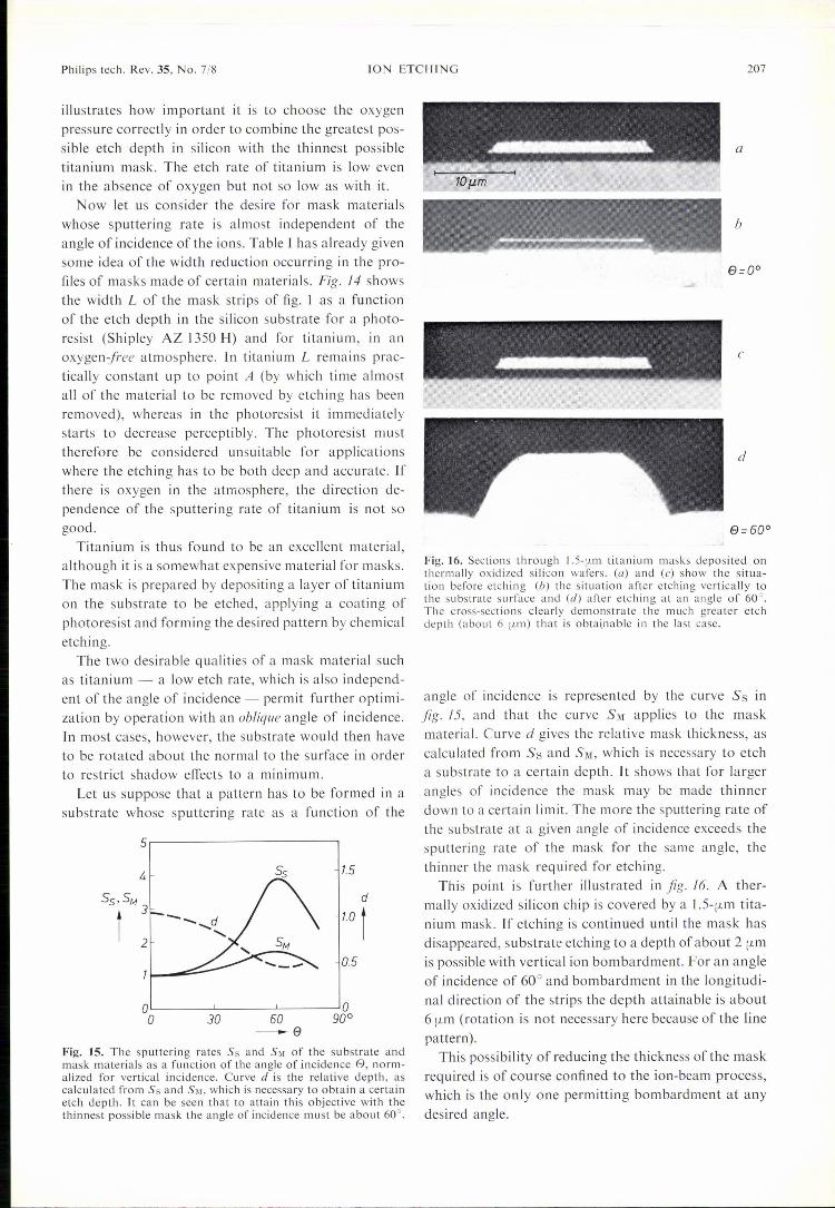
illustrates how important it is to choose the oxygenpressure correctly in order to combine the greatest pos-sible etch depth in silicon with the thinnest possibletitanium mask. The etch rate of titanium is low evenin the absence of oxygen but not so low as with it.
Now Jet us consider the desire for mask materialswhose sputtering rate is almost independent of theangle of incidence of the ions. Table I has already givensome idea of the width reduction occurring in the pro-files of masks made of certain materials. Fig. 14 showsthe width L of the mask strips of fig. I as a functionof the etch depth in the silicon substrate for a photo-resist (Shipley AZ 1350 H) and for titanium, in anoxygen~rree atmosphere. In titanium L remains prae-tically constant up to point A (by which time almostall of the material to be removed by etching has beenremoved), whereas in the photoresist it immediatelystarts to decrease perceptibly. The photoresist musttherefore be considered unsuitable for applicationswhere the etching has to be both deep and accurate. Ifthere is oxygen in the atmosphere, the direction de-pendence of the sputtering rate of titanium is not sogood.
Titanium is thus found to be an excellent material,although it is a somewhat expensive material for masks.The mask is prepared by depositing a layer of titaniumon the substrate to be etched, applying a coating ofphotoresist and forming the desired pattern by chemicaletching.
The two desirable qualities of a mask material suchas titanium - a low etch rate, which is also independ-ent of the angle of incidence - permit further optimi-zation by operation with an oblique angle of incidence.In most cases, however, the substrate would then haveto be rotated about the normal to the surface in orderto restrict shadow effects to a minimum.
Let us suppose that a pattern has to be formed in asubstrate whose sputtering rate as a function of the
5,---------------------,
1.54
0.5
OL_----~------~----~Oo w w ~o-19
Fig. 15. The sputtering rates Ss and SM of the substrate andmask materials as a function of the angle of incidence 6, norm-alized for vertical incidence. Curve d is the relative depth, ascalculated from Ss and SM, which is necessary to obtain a certainetch depth. It cao be seen that to attain this objective with thethinnest possible mask the angle of incidence must be about 60°.
a
b
6=0°
c
d
6=60°
Fig. 16. Sections through I.S-fJ.m titanium masks deposited onthermally oxidized silicon wafers. (a) and (c) show the situa-tion before etching (b) the situation after etching vertically tothe substrare surface and (d) after etching at an angle of 60°.The cross-sections clearly demonstrate the much greater etchdepth (about 6 fJ.m) that is obtainable in the last case.
angle of incidence is represented by the curve Ss infig. 15, and that the curve SM applies to the maskmaterial. Curve d gives the relative mask thickness, ascalculated from Ss and SM, which is necessary to etcha substrate to a certain depth. It shows that for Jargerangles of incidence the mask may be made thinnerdown to a certain limit. The more the sputtering rate ofthe substrate at a given angle of incidence exceeds thesputtering rate of the mask for the same angle, thethinner the mask required for etching.
This point is further illustrated in fig. 16. A ther-mally oxidized silicon chip is covered by a l.5-fLm tita-nium mask. If etching is continued until the mask hasdisappeared, su bstrate etching to a depth of about 2 p.mis possible with vertical ion bombardment. For an angleof incidence of 60° and bombardment in the longitudi-nal direction of the strips the depth attainable is about6 fLm(rotation is not necessary here because of the linepattern).
This possibility of reducing the thickness of the maskrequired is of course confined to the ion-beam process,which is the only one permitting bombardment at anydesired angle.
208 ION ETCHING Philips tech. Rev. 35, No. 7/8
Finally, to demonstrate the possibilities of ourmethod, we should like to refer to the title picture again.The mosaic-like pattern shown there of an epitaxialgarnet layer (with a periodicity of 20 !Lmand an etchdepth of 5.5 (.Lm) was achieved with the optimized ion-etching method just described. The mask was a tita-nium layer approximately 3 !Lmthick, and ion bom-bardment was carried out at an angle of 45° on arotating substrate. Had the 'optimum' angle of 60°been 'used, shadow effects would have restricted theattainable depth.
'.
Summary. With ion etching it is possible, for the same etch depthof, say, 1 (J.m,to form patterns with lateral dimensions (also I (J.m)that are approxirnately five times smaller than is possible withconventional chemical etching methods. Two currently practisedion-etching processes are r.f. cathode sputtering and ion-beametching. Research carried out at Philips ForschungslaboratoriumHamburg, has led to the following conclusions: back-diffusionmust be avoided as far as possible (which means that the ion-beam process will often be the most suitable method); the requiredratio of etch rates (Iow for the mask, high for the substrate)can be achieved very effectively with a titanium mask and etchingin an argon and oxygen atmosphere; sputtering must depend aslittle as possible on the angle ofincidence ofthe ions. With regardto this last point, titanium is again found to be an excellent maskmaterial. The best results are obtained with a titanium mask andbombardment at an oblique angle.