Embed Size (px)
Citation preview
N A S A T E C H N I C A L AB^BfBii MASA TM X-2676MEMORANDUM
-oev
AN INVESTIGATION OF OPTICAL FEEDBACKTO EXTEND THE FREQUENCY RESPONSEOF SOLID-STATE DETECTOR SYSTEMS
by Stephen J. Katzberg
Langley Research Center
Hampton, Va. 23365
NATIONAL AERONAUTICS AND SPACE ADMINISTRATION • WASHINGTON, D. C. * DECEMBER 1972
https://ntrs.nasa.gov/search.jsp?R=19730004703 2019-02-02T05:48:05+00:00Z
1. Report No.
NASA TM X-26762. Government Accession No. 3. Recipient's Catalog No.
4. Title and SubtitleAN INVESTIGATION OF OPTICAL FEEDBACK TOEXTEND THE FREQUENCY RESPONSE OF SOLID-STATEDETECTOR SYSTEMS
5. Report Date
December 19726. Performing Organization Code
7. Author(s)
Stephen J. Katzberg
8. Performing Organization Report No.
L-8590
9. Performing Organization Name and Address
NASA Langley Research CenterHampton, Va. 23365
10. Work Unit No.
502-03-52-0411. Contract or Grant No.
12. Sponsoring Agency Name and Address . ,. . '' •
National Aeronautics and Space AdministrationWashington, D.C. 20546
13. Type of Report and Period Covered
Technical Memorandum14. Sponsoring Agency Code
15. Supplementary Notes
16. Abstract
A primary limitation of many solid-state photodetectors used in electro-optical sys-tems such as the facsimile camera is their slow response in converting light intensitiesinto electrical signals. An optical feedback technique is presented which can extend thefrequency response of systems that use these detectors by orders of magnitude withoutsignificantly degrading their signal-to-noise performance. This technique is analyzed topredict improvement, implemented, and evaluated to verify analytical results.
17. Key Words (Suggested by Author(s))
PhotodetectionWide bandOptical feedbackBandwidth expansionSolid-state detector system
18. Distribution Statement
Unclassified — Unlimited
19. Security Cfassif. (of this report)
Unclassified
20. Security Classif. (of this page)
Unclassified
21. No. of Pages
11
22. Price*
$3.00
For sale by the National Technical Information Service, Springfield, Virginia 22151
AN INVESTIGATION OF OPTICAL FEEDBACK
TO EXTEND THE FREQUENCY RESPONSE
OF SOLID-STATE DETECTOR SYSTEMS
By Stephen J. KatzbergLangley Research Center
SUMMARY
A primary limitation of many solid-state photodetectors used in electro-optical sys-tems such as the facsimile camera is their slow response in converting light intensitiesinto electrical signals. An optical feedback technique is presented which can extend thefrequency response of systems that use these detectors by orders of magnitude withoutsignificantly degrading their signal-to-noise performance. This technique is analyzed topredict improvement, implemented, and evaluated to verify analytical results.
INTRODUCTION
Only a few types of solid-state detectors currently available for electro-opticalsystems such as facsimile cameras would allow angular resolution of a few tenths of adegree or less with a wide depth of field constraint. The most important four are silicon(Si), lead sulfide (PbS), lead selenide (PbSe), and cadmium sulfide (CdS) photoconductors.All these diodes are operable at room temperature, silicon covering the wavelength rangeof 0.4 to 1.1 /nm, lead sulfide the range of 1.0 to 3.5 /im, lead selenide the range of 1.0 to4.5 jiim, and cadmium sulfide the range of 0.3 to 0.5 jum. However, all these detectors,except silicon, have slow internal response which severely limits their application whenrapid scanning is required. A thorough discussion of these detectors and their limitationscan be found in reference 1.
What is required is a technique for the simple extension of detection frequencyresponse into the low kilohertz range which covers those frequencies generated by typicalfacsimile camera systems without appreciable degradation of noise performance.
The purpose of this paper is to present an optical feedback preamplifier techniquewhich, without significantly increasing noise, can significantly extend the bandwidth ofphotoconductive light sensors that are normally limited by internal response time. Spe-cial attention will be directed to lead sulfide because of its great importance as an infra-
red sensor. An experimental model will also be described, and test results will be pre-sented to verify the analysis.
SYMBOLS
A amplifier gain
D* detectivity, cm -hertz ' /watt
f frequency, hertz
G light-dependent conductance of photodetector, mhos
G\ conductance of photodetector, mhos
G>. A dark conductance of photodetector, mhos
I(jc average current of light-emitting diode, amperes
IN f rms noise current generated by light-emitting diode, amperes/hertz '
% PbS rms n°ise current generated by lead sulfide photodetector,amperes/hertz 1/2
K . first-order frequency-dependent incremental sensitivity of photodetector,mhos/watt
KT second-order frequency-dependent incremental sensitivity of photodetector,mhos/watt2
L light power, watts
Le effective bias radiant power, watts
Lf optical feedback power, watts
LJ video radiant power, watts
rms radiant noise of light-emitting diode, watts/hertz1/
electronic charge, 1.6 x 10~** coulomb
amplifier bias resistance, ohms
diode series resistance, ohms
Rf feedback resistance, ohms
SD feedback-light coupling factor, watts/ampere
V supply voltage, volts
VB amplifier offset bias, volts
Vo output signal, volts
Vs detector bias, volts
a. normalized relative spectral responsivity of photodetector
X radiation wavelength, jam
A increment
Subscript:
max maximum
ANALYTICAL MODEL
A circuit that can improve video bandwidth by the optical feedback technique isshown in figure 1. This circuit consists basically of a high-gain light-to-voltage con-verter with the frequency-limited nonlinear photoconductor inside the feedback loop.The feedback element in this case is an infrared-emitting diode whose light-out versuscurrent-in characteristic is linear over several decades.
The relations governing the basic operation of this system will now be described.The following standard equation describes the output of the operational amplifier (seeref. 2):
-V0 = VsRjGx + VB (1)
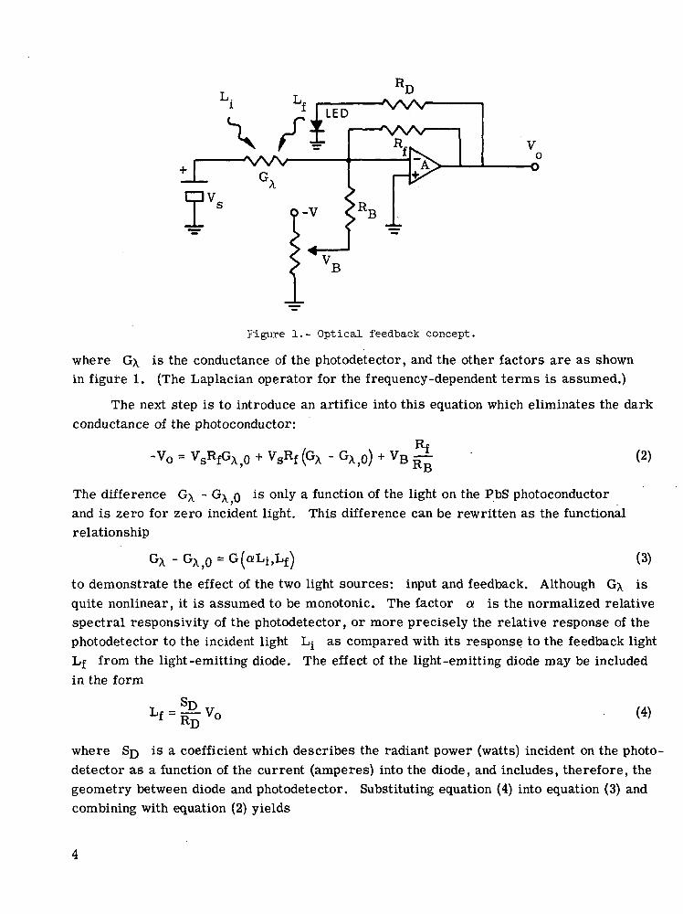
Figure 1.- Optical feedback concept.
where G\ is the conductance of the photodetector, and the other factors are as shownin figure 1. (The Laplacian operator for the frequency-dependent terms is assumed.)
The next step is to introduce an artifice into this equation which eliminates the darkconductance of the photoconductor:
-V = VsRf (2)
The difference GX - Gx Q is only a function of the light on the PbS photoconductor
and is zero for zero incident light. This difference can be rewritten as the functionalrelationship
GX - GX^Q = G(aLi,Lf j (3)
to demonstrate the effect of the two light sources: input and feedback. Although G\ isquite nonlinear, it is assumed to be monotonic. The factor a is the normalized relativespectral responsivity of the photodetector, or more precisely the relative response of thephotodetector to the incident light L^ as compared with its response to the feedback lightLf from the light-emitting diode. The effect of the light-emitting diode may be includedin the form
«~'o (4)
where SD is a coefficient which describes the radiant power (watts) incident on the photo-detector as a function of the current (amperes) into the diode, and includes, therefore, thegeometry between diode and photodetector. Substituting equation (4) into equation (3) andcombining with equation (2) yields
-V0 = VsRfGX}0 + VsRfG Lif Vo + VB (5)
Equation (5) may be linearized around the operating point Gx Q to make it takea form more like a standard feedback system:
-V0 « VsRfGx>0 + VgRfK AL + VB t (6)
snwhere AL = aLj + -=— Vo and K is defined in the expansion of equation (7):RD
GA - GA,O = G
= KAL+ |K ' (AL) 2 + . . . (7)£t
Both K and K* carry the frequency dependence of the photoconductor. Rewriting equa-tion (6) with a little manipulation gives, to first order,
(8a)l + V s R f K
If the loop gain VgRfK =^- is much greater than unity, equation (8a) becomesRD
v° = • ̂ (VAG*'° * VB Sfe ' % *L' (8b)
or, more conveniently,
Je (8c)SD BD
where
_!_/ Rj\e v~f) ir I S I A.O B-p IKRfVs y RB J
The formulation given by equation (8c) reveals two important points:
(1) The only sensitivity to the photodetector frequency response is in the removableconstant term Le. For this configuration, until the loop gain approaches unity the input-output frequency response to light will be determined by the feedback diode frequencyresponse (which is generally flat to several megahertz). As the loop gain approachesunity, the input-output response will again be dominated by the photodetector frequencyresponse. Put another way, the product of system gain and bandwidth for a high loop gainis constant. Thus, a loop gain of 10 will increase the "detection" frequency response bya factor of 10 ove'r that of the photoconductor itself, while a loop gain of 100 will increasefrequency response by a factor of 100, and so on.
(2) The output voltage is linear with respect to the input light L^. This resultrepresents the familiar linearizing effect of feedback. Although important, this result isnot as critical as poor frequency response in the detection of low light levels commonlyencountered in facsimile cameras, and it is not further pursued here.
EXPERIMENTAL MODEL AND RESULTS
Frequency Response
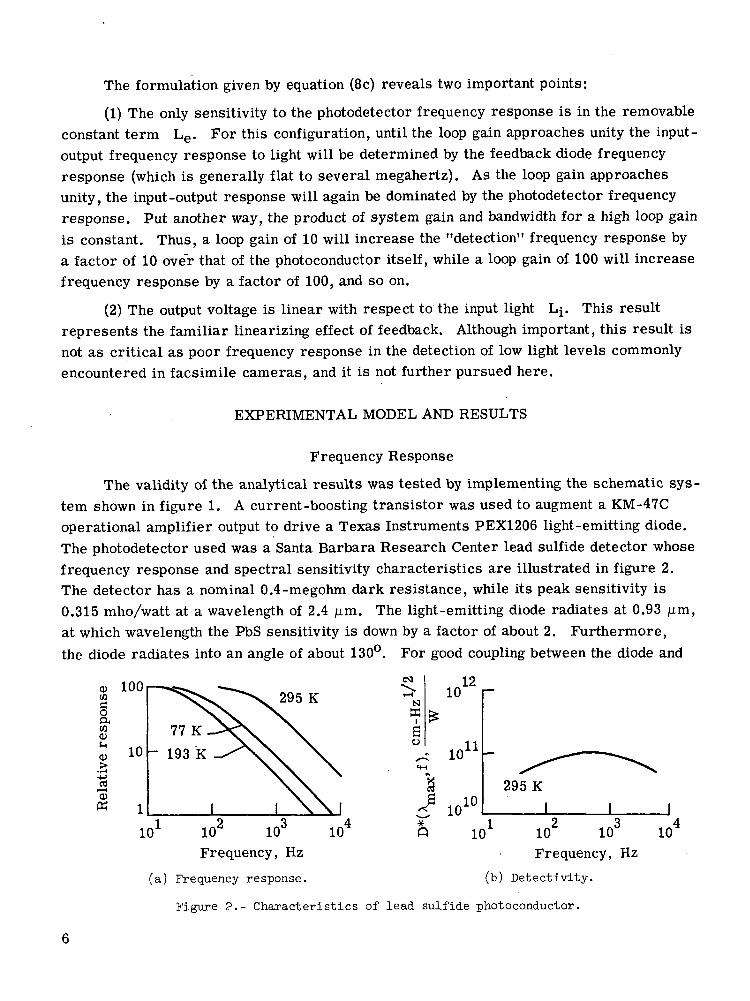
The validity of the analytical results was tested by implementing the schematic sys-tem shown in figure 1. A current-boosting transistor was used to augment a KM-47Coperational amplifier output to drive a Texas Instruments PEX1206 light-emitting diode.The photodetector used was a Santa Barbara Research Center lead sulfide detector whosefrequency response and spectral sensitivity characteristics are illustrated in figure 2.The detector has a nominal 0.4-megohm dark resistance, while its peak sensitivity is0.315 mho/watt at a wavelength of 2.4 j^m. The light-emitting diode radiates at 0.93 p.m,at which wavelength the PbS sensitivity is down by a factor of about 2. Furthermore,the diode radiates into an angle of about 130°. For good coupling between the diode and
woaeno
a>
100
10
295 K NKiso
1012
- 193 1011
a10
10295 K
I I
10 10 1010 10
Frequency, Hz
(a) Frequency response.
Figure 2.- Characteristics of lead sulfide photoconductor
10 10Frequency, Hz
(b) Detectivity.
10
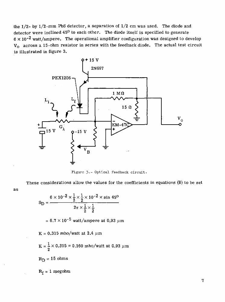
the 1/2- by 1/2-mm PbS detector, a separation of 1/2 cm was used. The diode anddetector were inclined 45° to each other. The diode itself is specified to generate6 X 10~2 watt/ampere. The operational amplifier configuration was designed to developVo across a 15-ohm resistor in series with the feedback diode. The actual test circuitis illustrated in figure 3.
PEX1206
as
Figure J.- Optical feedback circuit.
These considerations allow the values for the coefficients in equations (8) to be set
6 x ID'2 x I x I x 10'2 x sin 45°
2ir x I x I2 2
= 6.7 x 10~5 watt/ampere at 0.93 /urn
K = 0.315 mho/watt at 2.4 jum
K = - x 0.315 * 0.160 mho/watt at 0.93 p.m2
RD =15 ohms
= 1 megohm
Vs = 15 volts
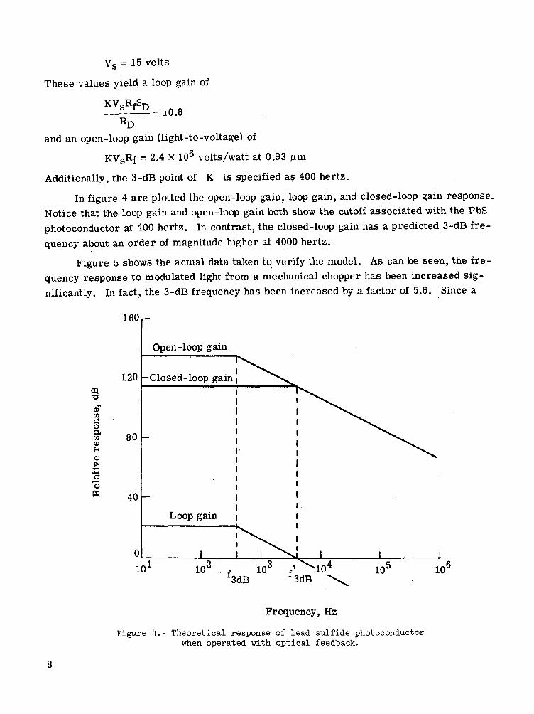
These values yield a loop gain of
KVsRfSD
R= 10.8
Dand an open-loop gain (light-to-voltage) of
KVsRf = 2.4 x 10⁶ volts/watt at 0.93
Additionally, the 3-dB point of K is specified as 400 hertz.
In figure 4 are plotted the open-loop gain, loop gain, and closed-loop gain response.Notice that the loop gain and open-loop gain both show the cutoff associated with the PbSphotoconductor at 400 hertz. In contrast, the closed-loop gain has a predicted 3-dB fre-quency about an order of magnitude higher at 4000 hertz.
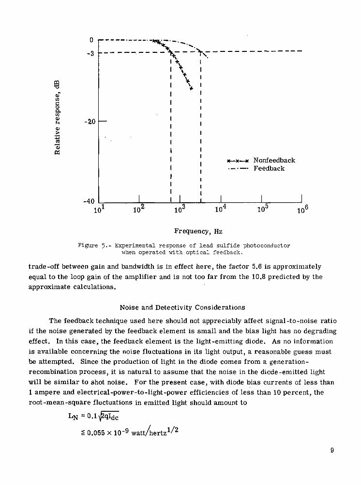
Figure 5 shows the actual data taken to verify the model. As can be seen, the fre-quency response to modulated light from a mechanical chopper has been increased sig-nificantly. In fact, the 3-dB frequency has been increased by a factor of 5.6. Since a
PQT3
«t
0)CO
COa>
CDK
160.-
120 —Closed-loop gain
80
40
Open-loop gain.
Loop gain
10J
f3dB 3dB
Frequency, Hz
Figure k.- Theoretical response of lead sulfide photoconductorwhen operated with optical feedback.
CDCOgaCO(Of-l
•r— (0)K
u
-3
-20
40
•"•••-%;
—
I
""*•>. '•v\1
r\
x— x — x NonfeedbackFeedback
I 1 1
10J 10' 10' 10-
Frequency, Hz
Figure 5.- Experimental response of lead sulfide photoconductorwhen operated with optical feedback.
trade-off between gain and bandwidth is in effect here, the factor 5.6 is approximatelyequal to the loop gain of the amplifier and is not too far from the 10.8 predicted by theapproximate calculations.
Noise and Detectivity Considerations
The feedback technique used here should not appreciably affect signal-to-noise ratioif the noise generated by the feedback element is small and the bias light has no degradingeffect. In this case, the feedback element is the light-emitting diode. As no informationis available concerning the noise fluctuations in its light output, a reasonable guess mustbe attempted. Since the production of light in the diode comes from a generation-recombination process, it is natural to assume that the noise in the diode-emitted lightwill be similar to shot noise. For the present case, with diode bias currents of less than1 ampere and electrical -power-to-light -power efficiencies of less than 10 percent, theroot-mean-square fluctuations in emitted light should amount to
Z 0.055 x ID'9 watt/hertz1/2
The feedback-light coupling factor Sp is the product of the basic light-emitting-dioderadiant power per ampere and the geometric coupling from diode to photodetector (PbS inthis case). Therefore, the noise power reaching the detector is
SD
60X10"3LN ~ 5.5 x 10"14 wattAertz1/2
Multiplying this radiant-noise power by the PbS conversion efficiency(203 amperes/watt) yields a noise current of
IN f = 12.5 X 1(T14 ampereAertz1/2
/ 1/2For comparison, the PbS internal noise is specified at approximately 2 juV/hertz ' at780 hertz. With an internal PbS impedance of 0.4 megohm this yields a detector-generated noise current of
IN pbg = 5 x 10~12 ampere/hertz '
Thus, comparison of the two noise currents, IN f and IN p^g, indicates that the feed-back element should contribute a negligible amount of noise to the system.
As was discussed earlier, the feedback system operates with a bias offset so thatthe sum of feedback light and input light is a constant. Another noise consideration is,therefore, the effect this bias level might have on the detectivity of the PbS photodetector.Since the effect of the bias light in this system is to cause a slight increase in PbS biascurrent, a slight decrease in detectivity may result if any change could be expected. Theeffect of photon noise inherent in the bias light should be negligible. Not all photodetec-tors have decreased detectivity with bias, and in fact other photoconductive devices showexactly the opposite effect. Each case will, therefore, have to be considered individually.
Experimentally it was observed that at 800 hertz the nonfeedback system gave6.0 ju.V of output noise in a 7-hertz bandwidth. When feedback was engaged and the sameoutput voltage was reestablished (thus setting the same current as before in the drivertransistor and PEX1206) the output noise was 1.2 ju.V in a 7-hertz bandwidth. This gavea ratio of 5:1, which is the loop gain determined earlier.
In other words, the feedback system does not appreciably affect signal-to-noiseratio, since both signal and noise are attenuated equally by the loop gain, justifying thequalitative conclusions concerning system noise performance.
CONCLUDING REMARKS
The principle of optical feedback offers a method for significantly improving thefrequency response of electro-optical systems that employ photodetectors with slow
10
internal response. As shown theoretically and experimentally, the improvement in band-width can be as high as the system loop gain - a result common to operational amplifiers.Furthermore, this technique does not necessarily introduce any appreciable degradationin noise performance. Finally, although a lead sulfide photodetector was chosen for theexperimental evaluation, the optical feedback technique can be applied profitably to otherdetectors with proper consideration of noise effects of the optical feedback element.
Langley Research Center,National Aeronautics and Space Administration,
Hampton, Va., November 21, 1972.
REFERENCES
1. Kruse, Paul W.; McGlauchlin, Laurence D.; and McQuistan, Richmond B.: Elements ofInfrared Technology. John Wiley & Sons, Inc., 1963.
2. Graeme, Jerald G.; Tobey, Gene E.; and Huelsman, Lawrence P., eds.: OperationalAmplifiers - Design and Applications. McGraw-Hill Book Co., Inc., c.1971.
NASA-Langley, 19.72 14 L-8590 11
NATIONAL AERONAUTICS AND SPACE ADMISTRATIONWASHINGTON, D.C. 20546
OFFICIAL. BUSINESS
f»£?MALT¥ FOR PRIVATE USE $30O FIRST CUSS MAIL
POSTAGE ANO FEES
NATIONAL AERONAUTICS AND
SPACE ADMINISTRATION
NASA 451
pric-ru iCTFB .FOSTMASTEK , I' Uodclivcuble ( Section 158£<> Noe Return
"The aeronautical and space activities of the United States shall beconducted so as to contribute . . . to the expansion of human knowl-edge of phenomena in the atmosphere and space. The Administrationshall provide for the widest practicable and appropriate disseminationof information concerning its activities and the results thereof."
— NATIONAL AERONAUTICS AND SPACE ACT OF 1958
NASA SCIENTIFIC AND TECHNICAL PUBLICATIONS
TECHNICAL RETORTS: Scientific andtechnical information considered important,complete, and a lasting contribution to existingknowledge,
TECHNICAL NOTES: Information less broadin scope but nevertheless of importance as acontribution to existing knowledge.
TECHNICAL MEMORANDUMS:Information receiving limited distributionbecause of preliminary data, security classifica-tion, (w other reasons,
CONTRACTOR REPORTS: Scientific andtechnical information generated under a NASAcontract or grant and considered an importantcontribution to existing knowledge.
TECHNICAL TRANSLATIONS: Informationpublished in a foreign language consideredto merit NASA distribution in English,
SPECIAL PUBLICATIONS: Informationderived from or of value to NASA activities.Publications include conference proceedings,monographs, data compilations, handbooks,sourcebooks, and special bibliographies,
TECHNOLOGY UTILIZATIONPUBLICATIONS: Information on technologyused by NASA that may be of particularinterest in commercial and other non-aerospaceapplications. Publications include Tech Briefs,Technology Utilization Reports andTechnology Surveys.
Details on the availability of these publications may be obtained from:
SCIENTIFIC AND TECHNICAL INFORMATION OFFICE
NATIONAL AERONAUTICS AND SPACE ADMINISTRATIONW«Kingion; D.C 20546
![Ultrasonic Methods for Human Motion Detection · Ultrasonic Methods for Human Motion Detection 9 - 2 RTO-MP-SET-107 UNCLASSIFIED/UNLIMITED UNCLASSIFIED/UNLIMITED measurements [1],](https://img.pdfslide.net/doc/110x75/5ae21e557f8b9ad47c8cabad/ultrasonic-methods-for-human-motion-methods-for-human-motion-detection-9-2-rto-mp-set-107.jpg)


![UNCLASSIFIED - Defense Technical Information …UNCLASSIFIED [Distribution Statement A] Approved for public release; distribution is unlimited (U) Applications of Miniaturized Atomic](https://img.pdfslide.net/doc/110x75/5ea8b329e9057c6c3e684174/unclassified-defense-technical-information-unclassified-distribution-statement.jpg)