Embed Size (px)
Citation preview

An probing evaluation of Cu-Pillar by using wire type Probe Card
Chang-Hoon, HyunSamsung Electronics

Contents• Probe Card cost of Cu-Pillar probing• Cases introduction of Cu-Pillar probing
- Temperature & Pad structure• An experience of Cu-Pillar probing by wire type • Process change for cost reduction• SEC Requirement of Cu-Pillar Flip-Chip Probing• Probe Card long life (MEMS Vertical) • Summary
2C.H Hyun
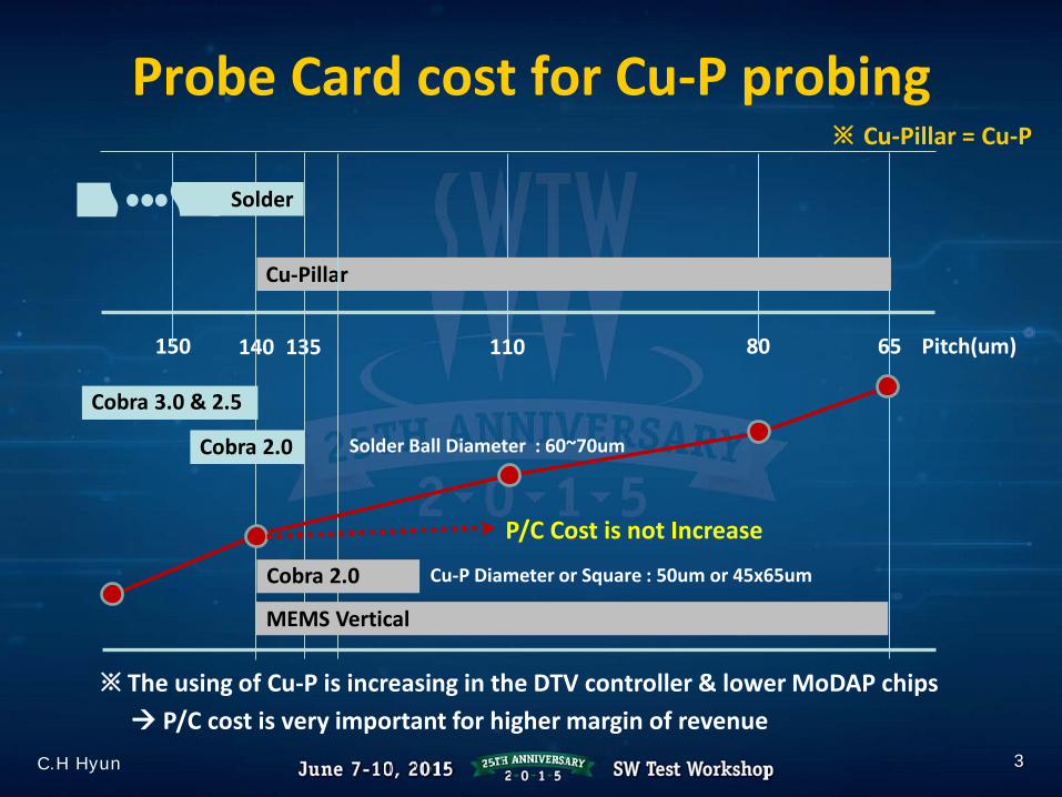
Probe Card cost for Cu-P probing
3
150 140 135 110 80 65 Pitch(um)
Solder
Cu-Pillar
※ Cu-Pillar = Cu-P
C.H Hyun
Cobra 3.0 & 2.5
Cobra 2.0
Cobra 2.0
MEMS Vertical
Cu-P Diameter or Square : 50um or 45x65um
Solder Ball Diameter : 60~70um
P/C Cost is not Increase
※ The using of Cu-P is increasing in the DTV controller & lower MoDAP chips P/C cost is very important for higher margin of revenue

Test case of Cu-P probing
4C.H Hyun
TCFC : Thermal Compression Flip Chip CuBOL : Copper-column Bond on Lead
A. Cu-P Structure Introduction
Source : Hamid Eslampour(STATSChipPAC)“Low Cost Cu Colimn fcPOP Technology “
IEEE, EMTC, 2012
Al pad
PI
UBMCu Plating
Ni Plating
Solder tip(SnAg)
Source : DIPSOL Website Figure http://www.dipsol-jp.com/wp-content/uploads/
bump_reflow_sem200.png
• Cu-P is expected to grow at CAGR(2014~2018) of 10~15% (SEC Case)- 2014 ~ 2015 : 28nm Controller/Modem (Room Temp) & MoDAP (Hot Temp)- 2016 ~ 2018 : 10~14nm Premium AP & 28nm Product(~beyond)- Mobile Phone Price drop down Improve PKG Cost Applying of Cu-P will expand
• The diameter limit of CuBol type is 40~45um 100um under pitch will be used TCFC
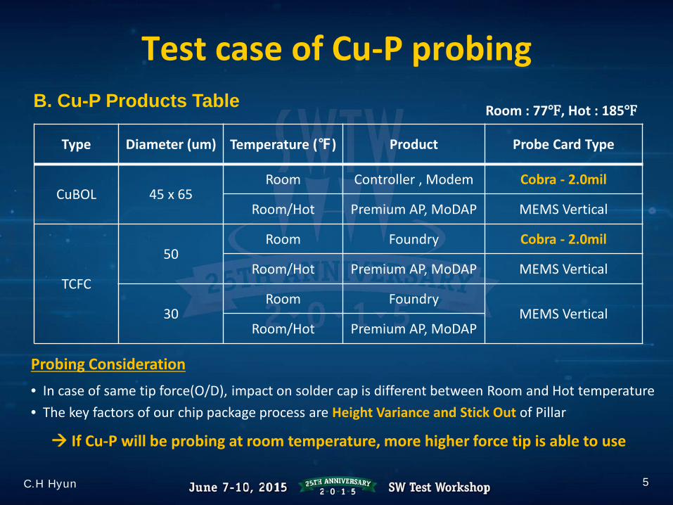
Test case of Cu-P probing
5
Type Diameter (um) Temperature (℉) Product Probe Card Type
CuBOL 45 x 65Room Controller , Modem Cobra - 2.0mil
Room/Hot Premium AP, MoDAP MEMS Vertical
TCFC
50Room Foundry Cobra - 2.0mil
Room/Hot Premium AP, MoDAP MEMS Vertical
30Room Foundry
MEMS VerticalRoom/Hot Premium AP, MoDAP
C.H Hyun
B. Cu-P Products Table Room : 77℉, Hot : 185℉
Probing Consideration • In case of same tip force(O/D), impact on solder cap is different between Room and Hot temperature • The key factors of our chip package process are Height Variance and Stick Out of Pillar
If Cu-P will be probing at room temperature, more higher force tip is able to use
Evaluation result by using wire type
6C.H Hyun
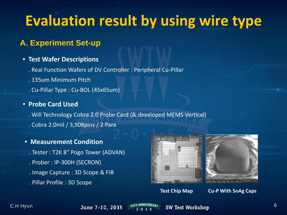
A. Experiment Set-up
• Test Wafer Descriptions. Real Function Wafers of DV Controller : Peripheral Cu-Pillar . 135um Minimum Pitch. Cu-Pillar Type : Cu-BOL (45x65um)
• Probe Card Used. Will Technology Cobra 2.0 Probe Card (& developed MEMS Vertical). Cobra 2.0mil / 3,908pins / 2 Para
• Measurement Condition. Tester : T2K 8” Pogo Tower (ADVAN). Prober : IP-300H (SECRON) . Image Capture : 3D Scope & FIB. Pillar Profile : 3D Scope
Test Chip Map Cu-P With SnAg Caps
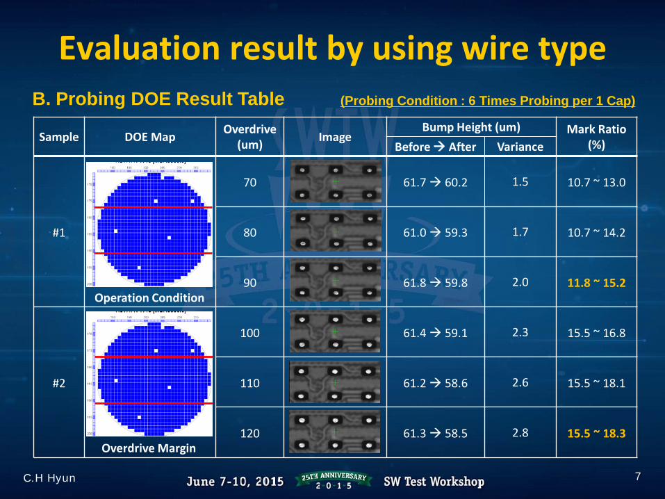
Sample DOE Map Overdrive(um) Image
Bump Height (um) Mark Ratio(%)Before After Variance
#1
70 61.7 60.2 1.5 10.7 ~ 13.0
80 61.0 59.3 1.7 10.7 ~ 14.2
90 61.8 59.8 2.0 11.8 ~ 15.2
#2
100 61.4 59.1 2.3 15.5 ~ 16.8
110 61.2 58.6 2.6 15.5 ~ 18.1
120 61.3 58.5 2.8 15.5 ~ 18.3
Evaluation result by using wire type
7C.H Hyun
B. Probing DOE Result Table (Probing Condition : 6 Times Probing per 1 Cap)
Operation Condition
Overdrive Margin

Evaluation result by using wire type
8C.H Hyun
C. 3D Scope Image : Production Product 80um 100um 120um
Top View
Side View
MeasureProbe X : 17.2umProbe Y : 22.9umBump Z : 63.8um
Probe X : 20.3umProbe Y : 23.7umBump Z : 61.3um
Probe X : 22.3umProbe Y : 27.4umBump Z : 60.8um
Room : 77℉
Evaluation result by using wire type
9C.H Hyun
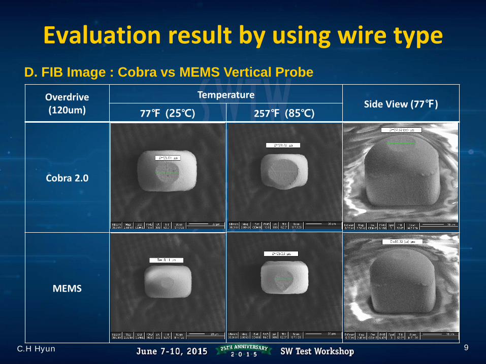
D. FIB Image : Cobra vs MEMS Vertical Probe Overdrive(120um)
TemperatureSide View (77℉)
77℉ (25℃) 257℉ (85℃)
Cobra 2.0
MEMS
Evaluation result by using wire type
10C.H Hyun
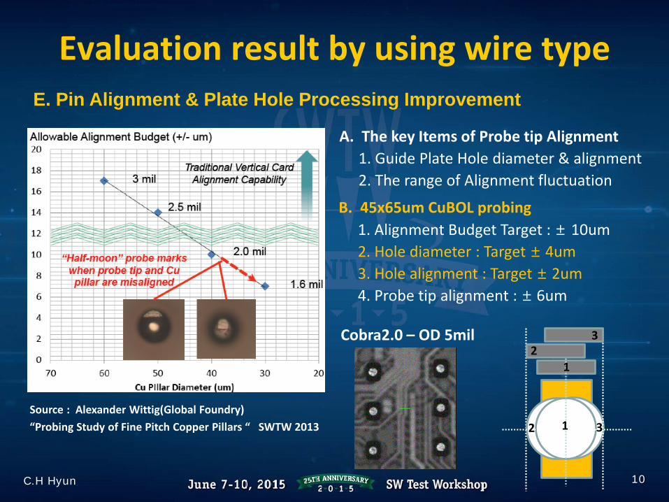
E. Pin Alignment & Plate Hole Processing Improvement
Source : Alexander Wittig(Global Foundry)“Probing Study of Fine Pitch Copper Pillars “ SWTW 2013
A. The key Items of Probe tip Alignment1. Guide Plate Hole diameter & alignment 2. The range of Alignment fluctuation
B. 45x65um CuBOL probing1. Alignment Budget Target : ± 10um2. Hole diameter : Target ± 4um3. Hole alignment : Target ± 2um 4. Probe tip alignment : ± 6um
Cobra2.0 – OD 5mil
12 3
12
3
Evaluation result by using wire type
11C.H Hyun
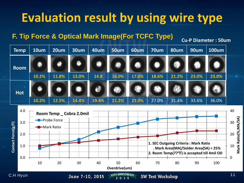
F. Tip Force & Optical Mark Image(For TCFC Type)
Temp 10um 20um 30um 40um 50um 60um 70um 80um 90um 100um
Room10.2% 11.8% 13.0% 14.8 16.0% 17.6% 18.6% 21.2% 23.0% 23.0%
Hot10.2% 12.5% 14.4% 19.4% 21.2% 23.0% 27.0% 31.4% 33.6% 36.0%
Cu-P Diameter : 50um
0
10
20
30
40
0.0
1.0
2.0
3.0
4.0
10 20 30 40 50 60 70 80 90 100
Probe Force
Mark Ratio
Room Temp _ Cobra 2.0mil
Overdrive(um)
Cont
act F
orce
(g/F
)
1. SEC Outgoing Criteria : Mark Ratio. Mark Area(MA)/Solder Area(SA) < 25%
2. Room Temp(77℉) is accepted till 4mil OD Mar
k Ra
tio(%
,MA/
SA)
Evaluation result by using wire type
12C.H Hyun
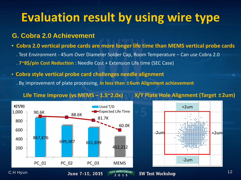
G. Cobra 2.0 Achievement
867,876 699,387 651,899
452,212
90.6K 88.6K 81.7K
60.0K
200
400
600
800
1,000
PC_01 PC_02 PC_03 MEMS
Used T/DExpected Life Time
K(T/D)
• Cobra 2.0 vertical probe cards are more longer life time than MEMS vertical probe cards. Test Environment - 45um Over Diameter Solder Cap, Room Temperature – Can use Cobra 2.0 . 7~8$/pin Cost Reduction : Needle Cost + Extension Life time (SEC Case)
• Cobra style vertical probe card challenges needle alignment . By improvement of plate processing, in less than ±6um Alignment achievement
-2um
-2um
+2um
+2um
X/Y Plate Hole Alignment (Target ±2um)Life Time Improve (vs MEMS – 1.5~2.0x)

Process change for cost reduction
13C.H Hyun
A. Cu-Pillar without Solder Cap
Source : Hao Chen(TSMC)“Wafer Level Chip Scale Package Copper Pillar Probing“
International Test Conference 2014, Seattle, Washington
• Essential Item Cu-P of under 30um diameter need to
Reflow process after probing
• Idea : without Solder Cap = Cu-P before Reflow
• Cost Improve(Bump ~ WLT) Reflow step change
Process change for cost reduction
14C.H Hyun
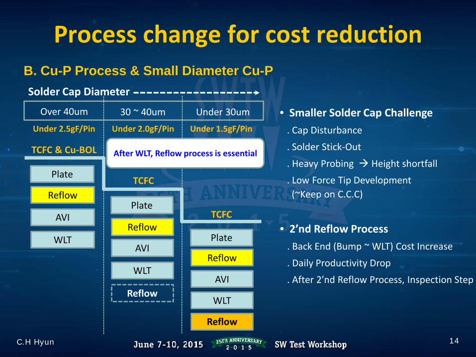
Solder Cap Diameter
TCFC & Cu-BOL
TCFC
TCFC
Over 40um 30 ~ 40um Under 30um
Plate
Reflow
AVI
WLT
Plate
Reflow
AVI
WLT
Reflow
Under 2.0gF/Pin Under 1.5gF/PinUnder 2.5gF/Pin
Plate
Reflow
AVI
WLT
Reflow
After WLT, Reflow process is essential
B. Cu-P Process & Small Diameter Cu-P
• Smaller Solder Cap Challenge. Cap Disturbance. Solder Stick-Out
. Heavy Probing Height shortfall
. Low Force Tip Development (~Keep on C.C.C)
• 2’nd Reflow Process. Back End (Bump ~ WLT) Cost Increase. Daily Productivity Drop . After 2’nd Reflow Process, Inspection Step
Process change for cost reduction
15C.H Hyun
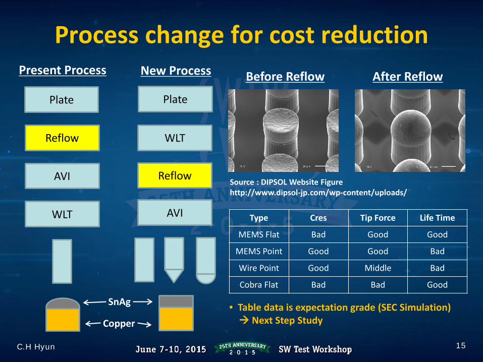
Plate
Reflow
AVI
WLT
Plate
Reflow
AVI
WLT
New ProcessPresent Process
SnAg
Copper
Before Reflow After Reflow
Source : DIPSOL Website Figure http://www.dipsol-jp.com/wp-content/uploads/
Type Cres Tip Force Life Time
MEMS Flat Bad Good Good
MEMS Point Good Good Bad
Wire Point Good Middle Bad
Cobra Flat Bad Bad Good
• Table data is expectation grade (SEC Simulation) Next Step Study

SEC Requirement of Flip-Chip Probing
16C.H Hyun
Items SOLDER Cu-Pillar
Pitch 150um ↑ 140-149um 135um ↓ 135um ↑ 110-135um 80-100um 65-80um
SolderDiameter 90um ↑ 80um 70um 50um 45um 45um 30um 25um
Needle Diameter 60~75Φ 60-75Φ 50~65Φ 50Φ ↓ 45*45um ↓ 30*30um ↓ 25*25um ↓
NeedleType Wire Wire Wire Wire
(Only Room Temp) MEMS & Etc Only MEMS Only MEMS
NeedleShape Flat Flat Flat Flat Flat Flat
(Point)Flat
(Point)
Tip Force(3mil) 7g ↓ 6g ↓ 4.5g ↓ 2.5g ↓ 2g ↓ 1.5g ↓ 1.5g ↓
C.C.C 800[mA] ↑ 800[mA] ↑
• In Solder Ball type, SEC will be using wire type Probe Card for long life realization - SEC Case : 2.0 ~ 2.5 Million Touch Down per 1 Probe Card
• Under 100um Cu-P product will be considering process change and MEMS point type

MEMS vertical probe - long life challenge
17C.H Hyun
• Usable Budget extension of Probe tip Length- Present Level : 300K ~ 500K T/D Goal : 1,000K T/D ( ~ 2016.03)
- Usable Budget of Tip Length : 250 ~ 270um Goal : 350um ( ~ 2016.06)
• Probe tip Cleaning Optimization- Cleaning Methodology : Polishing Pattern change ( ~ 2x Improved)
- Cleaning Sheet : 1um Lapping Film & Abrasive Material change ( ~ 2x Improved)
- Minimal Side Length : Tip Diameter 90% ( ~ 1.5x Improved)
• Probe tip Geometry & Materials Improvement- SEC Goal : 1.5 ~ 2.0 Million Touch Down per 1 Probe Card ( ~ 2017.01)
- SEC will consistently try to collaborate of Probe Card Maker
for new materials & new concept
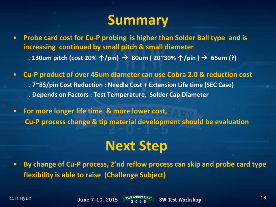
18C.H Hyun
• Probe card cost for Cu-P probing is higher than Solder Ball type and is increasing continued by small pitch & small diameter
. 130um pitch (cost 20% ↑/pin) 80um ( 20~30% ↑/pin ) 65um (?)
• Cu-P product of over 45um diameter can use Cobra 2.0 & reduction cost . 7~8$/pin Cost Reduction : Needle Cost + Extension Life time (SEC Case). Depends on Factors : Test Temperature, Solder Cap Diameter
• For more longer life time & more lower cost,Cu-P process change & tip material development should be evaluation
• By change of Cu-P process, 2’nd reflow process can skip and probe card typeflexibility is able to raise (Challenge Subject)
Next Step
Summary

Thank You.
19C.H Hyun
![June 1 – 4, 1997 San Diego, CA · • Gardell, Dave [IBM, Temperature Probing] • Gesse, Michelle [Advanced Probing Systems, Probe Potpourri] ... Mark Celentano Tri-Millenium Technology](https://img.pdfslide.net/doc/110x75/5fe3bcbd0ed22c1b5a4c0717/june-1-a-4-1997-san-diego-ca-a-gardell-dave-ibm-temperature-probing-a.jpg)