Embed Size (px)
Citation preview

Microelectronics Journal 87 (2019) 55–64
Contents lists available at ScienceDirect
Microelectronics Journal
journal homepage: www.elsevier.com/locate/mejo
An ultra-low voltage chaos-based true random number generator forIoT applications
Jen-Chieh Hsueh *, Vanessa H.-C. Chen
The Ohio-State University, Columbus, OH, 43210, USA
A R T I C L E I N F O
Keywords:Chaotic mapCryptographyEncryptionSecurityTrue random number generators (TRNGs)Ultra-low voltage (ULV)
* Corresponding author.E-mail address: [email protected] (J.-C. Hsueh)
https://doi.org/10.1016/j.mejo.2019.03.013Received 4 October 2018; Received in revised formAvailable online 3 April 20190026-2692/© 2019 Elsevier Ltd. All rights reserved
A B S T R A C T
Low-power consumption and low-voltage operation are critical enabling features for Internet of Things (IoT)devices that are powered from energy harvesting. This paper presents a chaos-based true random numbergenerator (TRNG) that can operate at an ultra-low voltage (ULV) and be integrated into energy-constrained IoTdevices for secure communications. Folded Bernoulli maps are adopted for random number generation. Switched-capacitor chaotic circuits utilize bulk-driven amplifiers to mitigate gate leakage issue, two-stage comparators toincrease voltage headroom, and low-complexity calibration schemes to ensure robustness. This system covers awide range of process and temperature variations while consuming 142 nW from a 0.4 V supply at a bit rate of10 kb/s. The generated bits pass National Institute of Standards and Technology (NIST) Pub-800.22 randomnesstests successfully.
1. Introduction
Internet-of-Things (IoT) is expected to grow into billions of devices inthe near future, revolutionizing various applications, such as continuoushealth monitoring and pervasive environmental sensing. To avoidfrequent battery replacement for many distributed devices, utilizing en-ergy harvested from an ambient environment provides a compelling so-lution to this challenge. However, the amount of power provided byenergy harvesters is limited and varies with environmental conditions,depending on the type of energy sources. For instance, energy harvestedfrom thermoelectric generators (TEGs) is highly temperature dependent[1,2]. Hence, in order to be powered by energy harvesters, the systemrequires consuming very low power and operating at an ultra-low voltage(ULV), which is less than 0.5 V [2–4].
Because IoT devices may transmit private and confidential informa-tion, secure communication becomes important, where a sequence ofrandom numbers is essential for secure encryption [5–7]. Both symmetricand asymmetric ciphering algorithms require high-quality randomnumbers to produce secret keys for encryption. The quality of the randomnumbers determines the performance of the encryption.
There are twomajor categories of random number generators (RNGs),pseudo-RNGs (PRNGs) and physical-RNGs, which are known as true-RNGs (TRNGs). PRNG algorithms expand a small random seed to pro-duce repeating and random-like sequences. Leaking of the seed can make
.
27 February 2019; Accepted 26
.
predicting outputs of the PRNG possible. On the contrary, TRNGs pro-duce the random numbers from a physical process or an observable ac-tivity that has true randomness. Therefore, TRNGs are preferred forcryptography applications.
Typical random sources of TRNGs are related to nondeterministicphysical processes, such as Johnson thermal noise, jitter in oscillators andrandom telegraph noise. Considering low magnitudes of the thermalnoise in resistor-based entropy sources, it requires a power-hungryamplifier to generate random numbers [8]. In addition to the directamplifying the thermal noise, metastable latches are used to generaterandom numbers as well [11,12]. Although the metastable latch cangenerate random numbers efficiently, it requires high-complexity cali-brations to cover process variations and entropy source mismatches.Another popular approach to generate random numbers is ring oscillatorsampling [13,23–25]. Conventionally, a slow and jittery clock samples afast clock to generate the random numbers. To ensure randomness, thejitter of the slow clock must be comparable to the oscillation period of thefast clock [13]. However, this method has low entropy issue due to thelimited jitter in a single ring oscillator. To increase the magnitude of theentropy source (jitter), inverter stages in ring oscillators are biased insubthreshold region, which reduces the power consumption as well [25].Random telegraph noise in devices are also used for generating randomnumbers [26]. In addition to pre-existing traps in devices, more traps canbe generated by hot carrier stress, which enhances the robustness as well
March 2019
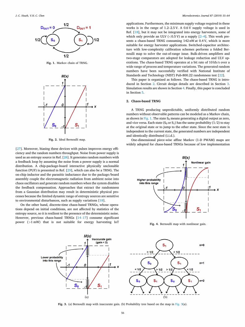
Fig. 1. Markov chain of TRNG.
Fig. 2. Ideal Bernoulli map.
Fig. 4. Bernoulli map with nonlinear gain.
J.-C. Hsueh, V.H.-C. Chen Microelectronics Journal 87 (2019) 55–64
[27]. Moreover, biasing these devices with pulses improves energy effi-ciency and the random numbers throughput. Noise from power supply isused as an entropy source in Ref. [28]. It generates random numbers witha feedback loop by assuming the noise from a power supply is a normaldistribution. A chip-package-board interactive physically unclonablefunction (PUF) is presented in Ref. [29], which can also be a TRNG. Theon-chip inductor and the parasitic inductance due to the package/boardassembly couple the electromagnetic radiation from ambient noise intochaos oscillators and generate random numbers when the system disablesthe feedback compensation. Approaches that extract the randomnessfrom a Gaussian distribution may result in deterministic physical pro-cesses because the limited dynamic range of entropy sources are sensitiveto environmental disturbances, such as supply variations [18].
On the other hand, discrete-time chaos-based TRNGs, whose opera-tions depend on initial conditions, are not affected by statistics of theentropy source, so it is resilient to the presence of the deterministic noise.However, previous chaos-based TRNGs [14–17] consume significantpower (>1mW) that is not suitable for energy harvesting IoT
Fig. 3. (a) Bernoulli map with inaccurate gain. (b)
56
applications. Furthermore, the minimum supply voltage required in theseworks is in the range of 1.2–2.5 V. A 0.6 V supply voltage is used inRef. [18], but it may not be integrated into energy harvesters, some ofwhich only provide an ULV (<0.5 V) as a supply [2–4]. This work pre-sents a chaos-based TRNG consuming 142 nW at 0.4 V, which is moresuitable for energy harvester applications. Switched-capacitor architec-ture with low-complexity calibration schemes performs a folded Ber-noulli map to solve the out-of-range issue. Bulk-driven amplifiers andtwo-stage comparators are adopted for leakage reduction and ULV op-erations. The chaos-based TRNG operates at a bit rate of 10 kb/s over awide range of process and temperature variations. The generated randomnumbers have been successfully verified with National Institute ofStandards and Technology (NIST) Pub-800.22 randomness test [22].
This paper is organized as follows. The chaos-based TRNG is intro-duced in Section 2. Circuit design details are described in Section 3.Simulation results are shown in Section 4. Finally, this paper is concludedin Section 5.
2. Chaos-based TRNG
A TRNG producing unpredictable, uniformly distributed randomnumbers without observable patterns can be modeled as a Markov chain,as shown in Fig. 1. The state S0 means generating a digital output as zero,and vice versa. Each state (S0 or S1) has the same probability (1/2) to stayat the original state or to jump to the other state. Since the next state isindependent to the current state, the generated numbers are independentand identically distributed (i.i.d.).
One-dimensional piece-wise affine Markov (1-D PWAM) maps arewidely adopted for chaos-based TRNGs because of low implementation
Probability tree based on the map in Fig. 3(a).
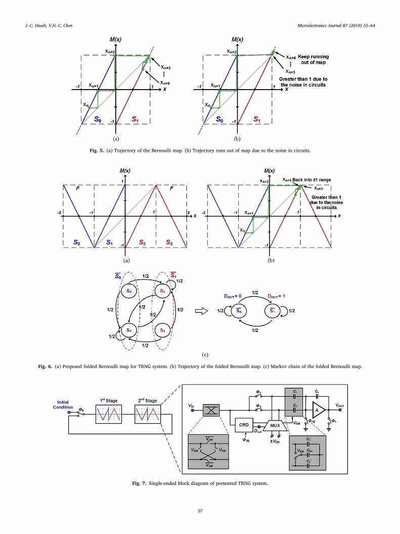
Fig. 5. (a) Trajectory of the Bernoulli map. (b) Trajectory runs out of map due to the noise in circuits.
Fig. 6. (a) Proposed folded Bernoulli map for TRNG system. (b) Trajectory of the folded Bernoulli map. (c) Markov chain of the folded Bernoulli map.
Fig. 7. Single-ended block diagram of presented TRNG system.
J.-C. Hsueh, V.H.-C. Chen Microelectronics Journal 87 (2019) 55–64
57
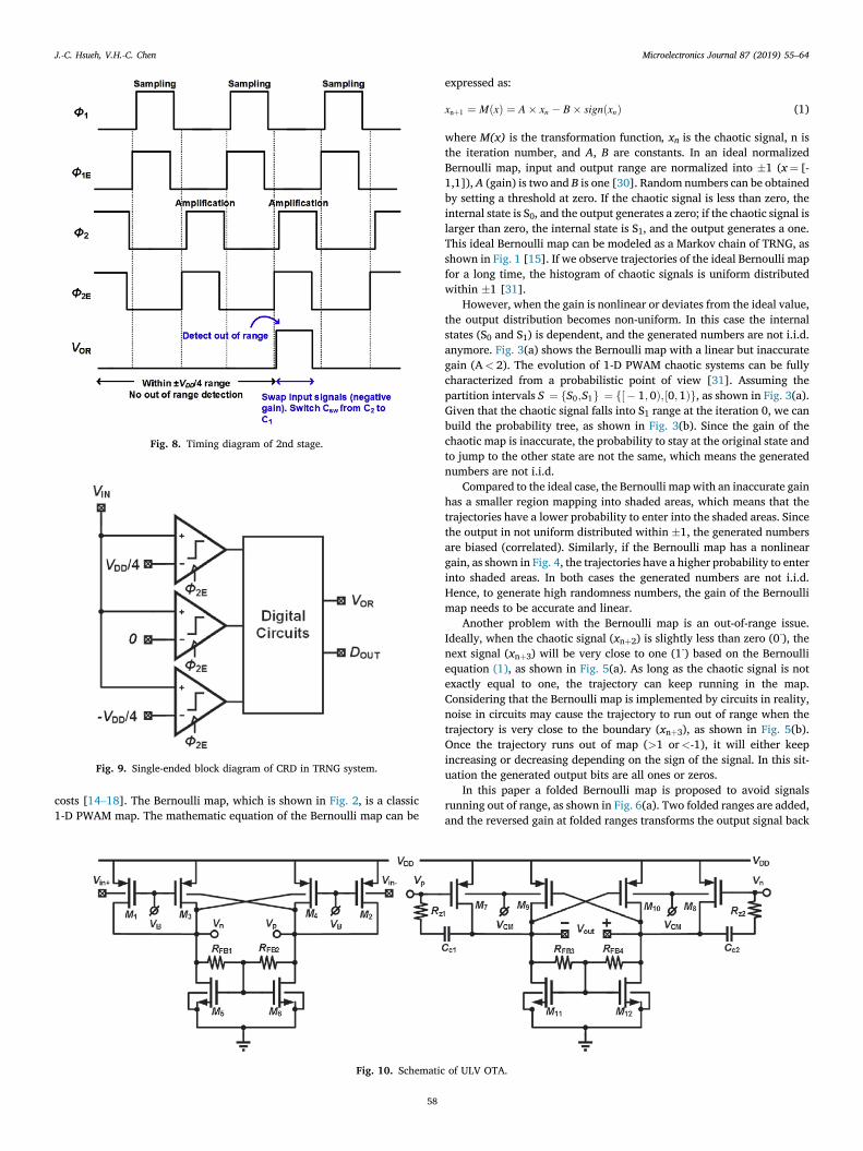
Fig. 8. Timing diagram of 2nd stage.
Fig. 9. Single-ended block diagram of CRD in TRNG system.
J.-C. Hsueh, V.H.-C. Chen Microelectronics Journal 87 (2019) 55–64
costs [14–18]. The Bernoulli map, which is shown in Fig. 2, is a classic1-D PWAM map. The mathematic equation of the Bernoulli map can be
Fig. 10. Schematic
58
expressed as:
xnþ1 ¼ MðxÞ ¼ A� xn � B� signðxnÞ (1)
where M(x) is the transformation function, xn is the chaotic signal, n isthe iteration number, and A, B are constants. In an ideal normalizedBernoulli map, input and output range are normalized into �1 (x¼ [-1,1]), A (gain) is two and B is one [30]. Random numbers can be obtainedby setting a threshold at zero. If the chaotic signal is less than zero, theinternal state is S0, and the output generates a zero; if the chaotic signal islarger than zero, the internal state is S1, and the output generates a one.This ideal Bernoulli map can be modeled as a Markov chain of TRNG, asshown in Fig. 1 [15]. If we observe trajectories of the ideal Bernoulli mapfor a long time, the histogram of chaotic signals is uniform distributedwithin �1 [31].
However, when the gain is nonlinear or deviates from the ideal value,the output distribution becomes non-uniform. In this case the internalstates (S0 and S1) is dependent, and the generated numbers are not i.i.d.anymore. Fig. 3(a) shows the Bernoulli map with a linear but inaccurategain (A< 2). The evolution of 1-D PWAM chaotic systems can be fullycharacterized from a probabilistic point of view [31]. Assuming thepartition intervals S ¼ fS0;S1g ¼ f½� 1;0Þ;½0;1Þg, as shown in Fig. 3(a).Given that the chaotic signal falls into S1 range at the iteration 0, we canbuild the probability tree, as shown in Fig. 3(b). Since the gain of thechaotic map is inaccurate, the probability to stay at the original state andto jump to the other state are not the same, which means the generatednumbers are not i.i.d.
Compared to the ideal case, the Bernoulli map with an inaccurate gainhas a smaller region mapping into shaded areas, which means that thetrajectories have a lower probability to enter into the shaded areas. Sincethe output in not uniform distributed within �1, the generated numbersare biased (correlated). Similarly, if the Bernoulli map has a nonlineargain, as shown in Fig. 4, the trajectories have a higher probability to enterinto shaded areas. In both cases the generated numbers are not i.i.d.Hence, to generate high randomness numbers, the gain of the Bernoullimap needs to be accurate and linear.
Another problem with the Bernoulli map is an out-of-range issue.Ideally, when the chaotic signal (xnþ2) is slightly less than zero (0-), thenext signal (xnþ3) will be very close to one (1-) based on the Bernoulliequation (1), as shown in Fig. 5(a). As long as the chaotic signal is notexactly equal to one, the trajectory can keep running in the map.Considering that the Bernoulli map is implemented by circuits in reality,noise in circuits may cause the trajectory to run out of range when thetrajectory is very close to the boundary (xnþ3), as shown in Fig. 5(b).Once the trajectory runs out of map (>1 or<-1), it will either keepincreasing or decreasing depending on the sign of the signal. In this sit-uation the generated output bits are all ones or zeros.
In this paper a folded Bernoulli map is proposed to avoid signalsrunning out of range, as shown in Fig. 6(a). Two folded ranges are added,and the reversed gain at folded ranges transforms the output signal back
of ULV OTA.

Fig. 11. Calibration circuits for resistors in OTA. The input-referred white noise spectral density (V2/Hz) of the first stage OTA IRN1 is given by.
Fig. 12. (a) Output range shifting due to the OTA offset. (b) Shifting thethresholds of the next transformation function to resolve the offset issue.
J.-C. Hsueh, V.H.-C. Chen Microelectronics Journal 87 (2019) 55–64
into �1 range, as shown in Fig. 6(b). With the two folded ranges, thetrajectories will not suffer from out-of-range issues. The transformationfunction M(x) of the folded Bernoulli map can be expressed as:
xnþ1 ¼ MðxnÞ ¼�
2xn � signðxnÞ; jxj < 1�ð2xn � 3signðxnÞÞ; jxj � 1
(2)
When the input signal is beyond �1 range, not only the gain becomesnegative, the coefficient of the last term in (2) also increases by threetimes.
Assuming the partition intervals S ¼ fS0;S1;S2;S3g ¼ f½� 2; � 1Þ; ½ �1;0Þ; ½0; 1Þ; ½1;2Þg, as shown in Fig. 6(a), the evolution of the system canbe described by the four-state Markov chain as shown in Fig. 6(c). We canname two macro-states S0 ¼ fS0; S1g and S1 ¼ fS2;S3g. The new macro-states diagram is exactly the same as the Markov chain in Fig. 1. In otherwords, the folded Bernoulli map can be used to generate true randomnumbers. Further detailed circuits discussion will be shown in the nextsection.
3. Circuit implementation
A low supply voltage diminishes a voltage headroom of an amplifier.Hence, it is challenging to achieve a linear gain with an ULV supply. Asingle-ended block diagram of presented TRNG is shown in Fig. 7 forclarity, but the actual circuits are operated in fully differential mode. TheTRNG system has two stages. Each stage implements the folded Bernoullimap. Although a higher throughput of random numbers can be achievedby cascadingmore stages, the power consumption of the system increasesas well. Considering the throughput and the total power consumption,two stages are chosen in this TRNG system.
A sub-ranging closed-loop architecture is adopted for implementingthe linear gain in the folded Bernoulli map. An initial value of the foldedBernoulli map is set by an initial condition during the first cycle,Φ0. Afterthat, the output of the second stage connects to the input of the first stageto form a positive feedback loop for random number generation.
Each stage operates in two modes, sampling and amplification. When1st stage is in amplification mode, 2nd stage is in sampling mode (sam-ples the 1st stage output), and vice versa. The timing diagram of 2ndstage is shown in Fig. 8, whereΦ1 andΦ2 are two non-overlapping clocks.When Φ1 is high, the 2nd stage is at the sampling mode. C1, and C2sample the input voltage while C3 is in reset. When Φ1 goes low and Φ2goes high, the 2nd stage is at the amplification mode, in which the chargestored on C1 and C2 transfers to C3. The comparator and range detectors(CRD) are clocked at Φ2E, which is slightly early than Φ2, ensuring thatthe comparison results are ready to program reference voltages before
59
the charge is transferred to C3. When the input voltage is larger than zero,the top plate of C1 and C2 connect to VDD and -VDD during Φ2, respec-tively. The transfer function can be derived from the law of chargeconservation at the input node of the amplifier in two modes:

Table 1Transistors aspect ratio of the bulk-driven operational amplifier.
J.-C. Hsueh, V.H.-C. Chen Microelectronics Journal 87 (2019) 55–64
Vout ¼ C1 þ C2
C3Vin þ ðC2 � C1Þ
C3VDD (3)
Transistors W/L (unit)
M1, M2 4/4 (μm/μm)M3, M4 1/4 (μm/μm)M5, M6 5.9/5 (μm/μm)M13, M14 (RFB1, RFB2) 2.6/0.06 (μm/μm)M7, M8 1/3 (μm/μm)M9, M10 1/3 (μm/μm)M11, M12 3.6/8 (μm/μm)M15, M16 (Rz1, Rz2) 10/0.06 (μm/μm)Cc1, Cc2 60 (fF)RFB3, RFB4 3.3 (MΩ)
Table 2Operational amplifier performance summary.
TT corner25 �C
FF corner0 �C
SS corner125 �C
Supply (V) 0.4 V 0.4 V 0.4 VPower (nW) 56.2 77.4 124.6Open loop gain (dB) 53.5 53.9 53Phase margin (�) 53 43 48Unity gain frequency (kHz) 216 228 391THD @ 400mVp-p (diff.) (%) 0.4 0.3 0.4Input referred noise (nV/√Hz) 49 113 131Offset (standard deviation, mV) 16.6 15.5 17.6
where VDD is the supply voltage, which is 0.4 V in this work.A single-ended block diagram of the CRD is shown in Fig. 9 for clarity,
but the actual circuits are operated in fully differential mode. The CRDconsists of three comparators. One of the comparators with the referencevoltage set at zero to generate random numbers, and the other twocomparators with the reference voltages set at�VDD/4 to detect whetherthe input voltage is out of boundaries. Since the input and the out rangeare�VDD/4, the transformation function M(x) in (2) becomes
xnþ1 ¼ MðxÞ ¼
8>>><>>>:
2xn � signðxnÞ4
VDD; jxj < 14VDD
��2xn � 3signðxnÞ
4VDD
�; jxj � 1
4VDD
(4)
When the input voltage is in the normal range (within �VDD/4), thecontrol signal VOR is set to low. In this case, the switched-capacitor Csw isconnected in parallel with C2’, as shown in Fig. 7. Csw is used forchanging the capacitors ratio, which relating to the last term in (4). WhenVOR is low, the capacitances of C1, C2, and C3 are 45 fF, 35 fF, and 40 fF,respectively, which realize the signðxnÞVDD=4 in (4). When the out-of-range condition is detected, VOR goes high that the input signals areswapped for implementing a negative gain, and Csw is connected inparallel with C1
0. The capacitances of C1 and C2 become 55 fF and 25 fF,
which realize the 3 ⋅ signðxnÞVDD=4 in (4).The von Neumann post-processing [19], which is implemented in
MATLAB, is employed to reduce correlations in random numbers due tothe non-idealities of amplifiers. Based on MATLAB simulation results, the
Table 3Transistors aspect ratio of the two-stage comparator.
Transistors W/L (unit)
M1, M2 2/0.6 (μm/μm)M3, M4 2/0.6 (μm/μm)M5, M6 0.2/0.06 (μm/μm)M7, M8 0.2/0.06 (μm/μm)M9, M10 0.2/0.06 (μm/μm)M11, M12 0.2/0.06 (μm/μm)M13, M14 0.2/0.06 (μm/μm)M15, M16 0.2/0.06 (μm/μm)M17, M18 0.2/0.06 (μm/μm)
Fig. 15. Monte Carlo simulation of the two-stage comparator.
Fig. 13. Schematic of the two-stage comparator.
Fig. 14. Implementation of CDAC for the two-stage comparator offsetcalibration.
60
post-processing can output high-quality random numbers if the gain erroris within one percentage of the ideal value. To achieve an accurate gainafter fabrications, three 4-bit capacitor digital-to-analog converters(CDACs) are added next to C1, C2, and C3 to compensate for mismatcherrors of capacitors. Given that the capacitances have �10% variationsafter fabrications, the worst gain error occurs when the value of C1 and C2increase by 10%, while the value of C3 decreases by 10%.1
1 Usually the mismatch shifts in the same direction.
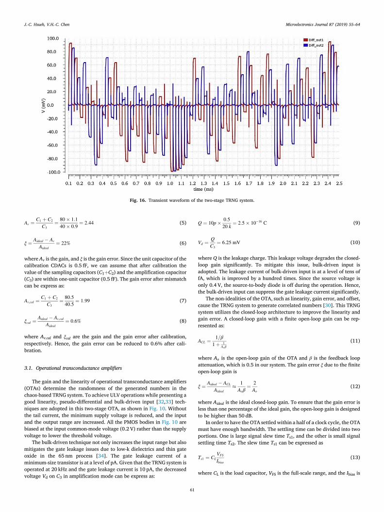
Fig. 16. Transient waveform of the two-stage TRNG system.
J.-C. Hsueh, V.H.-C. Chen Microelectronics Journal 87 (2019) 55–64
Av ¼ C1 þ C2
C3¼ 80� 1:1
40� 0:9¼ 2:44 (5)
ξ ¼ Aideal � Av
Aideal¼ 22% (6)
where Av is the gain, and ξ is the gain error. Since the unit capacitor of thecalibration CDACs is 0.5 fF, we can assume that after calibration thevalue of the sampling capacitors (C1þC2) and the amplification capacitor(C3) are within one-unit capacitor (0.5 fF). The gain error after mismatchcan be express as:
Av;cal ¼ C1 þ C2
C3¼ 80:5
40:5¼ 1:99 (7)
ξcal ¼Aideal � Av;cal
Aideal¼ 0:6% (8)
where Av;cal and ξcal are the gain and the gain error after calibration,respectively. Hence, the gain error can be reduced to 0.6% after cali-bration.
3.1. Operational transconductance amplifiers
The gain and the linearity of operational transconductance amplifiers(OTAs) determine the randomness of the generated numbers in thechaos-based TRNG system. To achieve ULV operations while presenting agood linearity, pseudo-differential and bulk-driven input [32,33] tech-niques are adopted in this two-stage OTA, as shown in Fig. 10. Withoutthe tail current, the minimum supply voltage is reduced, and the inputand the output range are increased. All the PMOS bodies in Fig. 10 arebiased at the input common-mode voltage (0.2 V) rather than the supplyvoltage to lower the threshold voltage.
The bulk-driven technique not only increases the input range but alsomitigates the gate leakage issues due to low-k dielectrics and thin gateoxide in the 65 nm process [34]. The gate leakage current of aminimum-size transistor is at a level of pA. Given that the TRNG system isoperated at 20 kHz and the gate leakage current is 10 pA, the decreasedvoltage Vd on C3 in amplification mode can be express as:
61
Q ¼ 10p� 0:520 k
¼ 2:5� 10�16 C (9)
Vd ¼ QC3
¼ 6:25 mV (10)
where Q is the leakage charge. This leakage voltage degrades the closed-loop gain significantly. To mitigate this issue, bulk-driven input isadopted. The leakage current of bulk-driven input is at a level of tens offA, which is improved by a hundred times. Since the source voltage isonly 0.4 V, the source-to-body diode is off during the operation. Hence,the bulk-driven input can suppress the gate leakage current significantly.
The non-idealities of the OTA, such as linearity, gain error, and offset,cause the TRNG system to generate correlated numbers [30]. This TRNGsystem utilizes the closed-loop architecture to improve the linearity andgain error. A closed-loop gain with a finite open-loop gain can be rep-resented as:
ACL ¼ 1=β1þ 1
Aoβ
(11)
where Ao is the open-loop gain of the OTA and β is the feedback loopattenuation, which is 0.5 in our system. The gain error ξ due to the finiteopen-loop gain is
ξ ¼ Aideal � ACL
Aideal� 1
Aoβ¼ 2
Ao(12)
where Aideal is the ideal closed-loop gain. To ensure that the gain error isless than one percentage of the ideal gain, the open-loop gain is designedto be higher than 50 dB.
In order to have the OTA settled within a half of a clock cycle, the OTAmust have enough bandwidth. The settling time can be divided into twoportions. One is large signal slew time Ts1, and the other is small signalsettling time Ts2. The slew time Ts1 can be expressed as
Ts1 ¼ CLVFS
Ibias(13)
where CL is the load capacitor, VFS is the full-scale range, and the Ibias is

J.-C. Hsueh, V.H.-C. Chen Microelectronics Journal 87 (2019) 55–64
the bias current. The CL is the OTA feedback capacitor which is 40 fF, VFSis VDD/4 which is 0.1 V, and the bias current in second stage of the OTA is24 nA. Hence, the slew time Ts1 can be calculated as 16.6 μs.
To settle within 1% error in half of a clock cycle (20 kHz), the smallsignal settling time should be less than 0.5Tclk - Ts1¼ 8.4 μs. The unitygain frequency fu of the OTA can be expressed as
fu � lnð100Þ2π ⋅ β ⋅ ð0:5Tclk � Ts1Þ (14)
where Tclk is the clock period. Substituting all the parameters into (14),the unity gain frequency needs to be larger than 175 kHz. To have somemargin, the unity gain frequency of the OTA is designed to be larger than200 kHz.
The cross-coupled pair M3-M4 in the first stage creates a negativebody transconductance, increasing the impedances at nodes Vn and Vp toboost the open-loop gain. The resistors RFB1-RFB2 detect the outputcommon-mode voltage and feed it back to drive the gates of M5-M6 as acommon-mode feedback loop. The second stage has a similar structurebut with gate-drive input. Since the second stage input is not connectedto the amplification capacitor (C3) and have smaller input swing, usinggate-driven input can has lower noise and higher efficiency. A high open-loop gain amplifier can be achieved by cascading these two stages, asshown in Fig. 10. The open-loop gain can be express as:
Fig. 17. The transformation function of the folded Bernoulli map atthree corners.
Fig. 18. Power consumption breakdown.
62
Av1 ¼ gmb1gds1 þ gds3 þ gds5 þ 1
RFB1� gmb3
(15)
Av2 ¼ gm7gds7 þ gds9 þ gds11 þ 1
RFB3� gm9
(16)
Av ¼ Av1 � Av2 (17)
where Av1 is the open-loop gain of the first stage, Av2 is the open-loopgain of the second stage, and Av is the total gain. The gmbN is the bodytransconductance of MN, the gmN is the transconductance of MN, and gdsNis the drain-source conductance of MN.
The high open-loop gain is obtained by adding the negative re-sistances at output nodes. If the negative transconductances deviate fromthe output impedances at Vn and Vp, the open-loop gain degradessignificantly. Hence, a calibration is essential for achieving a high open-loop gain after chip fabrications. The resistors, RFB1-RFB2 and Rz1-Rz2, areimplemented with transistors biased in subthreshold region to improvearea efficiency. The calibration scheme for impedance values of RFB1-RFB2 and Rz1-Rz2 is illustrated in Fig. 11. The tunable current (I1) gen-erates a control voltage (VCTRL) through a diode-connected load to biasthe MOSFET (M14) as a voltage-controlled resistor. Since the outputswing may result in the resistance value varying enormously, the localfeedback resistors, RFB3-RFB4, in the second stage are implemented by 6-bit non-silicide poly-resistors.
IRN1 ¼ 8kT � 23� 1gmb1
�gm1gmb1
þ gm3gmb1
þ gm5gmb1
�þ 2� 4kTg2mb1RFB1
(18)
The input-referred white noise spectral density (V2/Hz) of the secondstage OTA IRN2 and the total input-referred noise IRNtot are given by
IRN2 ¼ 8kT � 23� 1A2v1gm7
�1þ gm9
gm7þ gm11
gm7
�þ 2� 4kTA2v1g
2m7RFB3
(19)
IRNtot ¼ IRN1 þ IRN2 (20)
where Av1 is the first stage gain, which is shown in (15). This noise causesthe out-of-range issue in conventional Bernoulli map when the trajectoryis close to boundaries (�1). Thanks to the folded Bernoulli map, ourTRNG system does not have the out-of-range issue.
The offset of the OTA results in the output range shifting, which canbe resolved by shifting the detecting thresholds of the next stage with the
Table 4NIST test results after processing.
NIST Pub 800-22 Test TT corner25 �C
FF corner0 �C
SS corner125 �C
Result
Test P-value P-value P-value
Frequency 0.192 0.964 0.964 PassBlock Frequency 0.514 0.202 0.262 PassCumulative Sums (1) 0.172 0.798 0.122 PassCumulative Sums (2) 0.883 0.249 0.103 PassRuns 0.071 0.367 0.182 PassLongest Runs of 1's 0.163 0.936 0.596 PassRank 0.172 0.658 0.109 PassFFT 0.290 0.172 0.154 PassNon-overlapping Template Pass Pass Pass PassOverlapping Template 0.534 0.834 0.109 PassUniversal Statistical 0.637 0.868 0.237 PassApproximate Entropy 0.637 0.237 0.290 PassRandom Excursions Pass Pass Pass PassRandom Excursion Variant Pass Pass Pass PassSerial (1) 0.494 0.130 0.817 PassSerial (2) 0.475 0.616 0.851 PassLinear Complexity 0.851 0.534 0.851 Pass
* “Pass” means three corners and all sub-tests pass the statistical test.** The significance level in all tests is 0.01.

Table 5TRNG performance summary and comparison with recent publications.
[18] [23] [24] [25]* [27] [28] [29]** This work*
Technology 180 nm 180 nm 180 nm 65 nm 22 nm – 180 nm 65 nmEntropy Source Chaotic
SystemOscillator Jitter Oscillator Jitter Oscillator Jitter Telegraph Noise Power Supply Chaotic
SystemChaoticSystem
Supply Voltage (V) 0.6 0.8–1.8 1–1.8 1.2 – 5 1.8 0.4Bit Rate (Mb/s) 0.27 1.08/0.18 0.0005 96 2 – 3 0.01Power (μW) 0.082 109/3.7 0.015 123 – – 7920 0.142Efficiency (pJ/bit) 0.3 101/21 30 1.28 – – 2640 14.2
* Simulation Results. ** Physically Unclonable Function.
J.-C. Hsueh, V.H.-C. Chen Microelectronics Journal 87 (2019) 55–64
same amount. Assuming the OTA has an offset error Vos and the outputrange becomes (–VDD/4þVos, VDD/4þVos), as shown in Fig. 12(a). Aftershifting the detecting thresholds of the next transformation function withthe same amount, the output range of the transformation map is within�VDD/4 range, as shown in Fig. 12(b). To simplify the calibrationscheme, the offset of OTAs and comparators are calibrated together.
3.2. Comparator
The schematic of the two-stage dynamic comparators [20] for rangedetector is shown in Fig. 13, where the number of stacked transistors isreduced for ULV operation. The first stage is a preamplifier, followed by aregenerative latch as the second stage. When the clock is low, Vpren andVprep are pre-charged to VDD, pulling Vlatp, Vlatn and outputs to ground.When the clock is high, the comparator starts comparison. The inputdifferential pair draws different currents at Vpren and Vprep based on inputvoltages. When Vpren and Vprep are lower than the supply voltage minus athreshold voltage, Vlatp and Vlatn start charging the output latch forregeneration.
To calibrate the comparator offset, two 4-bit CDACs are added to Vprenand Vprep for offset cancellation. The unit capacitor of CDACs is imple-mented with a minimum-sized transistor (0.2 μm/0.06 μm), as shown inFig. 14. The source and drain are connected together as a MOS capacitorwhile the gate is connected with a switch controlled by a register [21].
4. Simulation results
The TRNG system is simulated in 65 nm CMOS technology with a20 kHz clock frequency. Table 1 shows the detail aspect ratio of the bulk-driven OTA, and the Table 2 shows the performance summary of the OTAat different corners. The simulation result shows that the OTA can ach-ieve enough linearity and open-loop gain at different corners.
The detail aspect ratio of the two-stage comparator is shown inTable 3. The sizes of the input differential pairs are increased fordecreasing offset voltage. The rest of the transistors are chosen to beminimum size for reducing parasitic capacitance. A thousand points ofMonte Carlo simulation is shown in Fig. 15, where the standard deviationof comparator offset is 4.2mV. The calibration range of CDACs in thecomparators is �25mV with a 1.6mV step size. The comparator offsetand the OTA offset are calibrated together by two 4-bit CDACs incomparators.
The transient waveform of the two-stage TRNG system is shown inFig. 16. The red line is the first-stage differential output, and the blue lineis the second-stage differential output. Both of the outputs work within�VDD/4 (�100mV) range as expected. The transformation function offolded Bernoulli map at different corners is shown in Fig. 17, where thegain is linear and accurate.
The TRNG system consumes 142 nW from a 0.4 V supply, and thepower consumption breakdown is shown in Fig. 18. Two amplifiersconsume 80% of the total power. The clock driver and digital logicsconsume 11% of the total power. The comparators and bias circuitsconsume 6% and 3% of the total power, respectively.
The randomness of numbers is evaluated by the NIST Pub-800.22 testsuite [22] with a hundred sequence of 1Mb data. Results of statistical
63
tests of randomness are represented in a form of P-values. The signifi-cance level is a parameter of NIST tests, chosen to be 0.01 as recom-mended by the NIST document. If the P-value is greater than or equal tothe significance level, it means that the sequence passes the statisticaltest. The bit rate of the TRNG system reduces from 40 kb/s to 10 kb/s dueto the von Neumann post-processing. The TRNG system is verified over awide range of process and temperature variations, including TT corner25 �C, FF corner 0 �C, and SS corner 125 �C at 0.4 V. All the generatedrandom numbers pass the NIST tests, as shown in Table 4. A 14.2 pJ/bitfigure of merit (FoM) has been achieved. The comparison results aresummarized in Table 5. Compared with state-of-the-arts, this work ach-ieves the lowest supply voltage (0.4 V), which is suitable for integratinginto energy harvesting IoT devices. Although the work in Ref. [18] hasgood efficiency, it may not fit in energy harvesting devices, some ofwhich can only provide ULV (<0.5 V) as a supply. The closed-loop ar-chitecture and low-complexity calibration schemes are adopted formaintaining the linearity of gain at ULV.
5. Conclusion
This work presents a chaos-based TRNG operating at 0.4 V. The TRNGcan be integrated into edge devices powered by energy harvested fromenvironment. In order to reliably produce random numbers over a widerange of process and temperature variations, this work utilizes switched-capacitor architecture with low-complexity calibration schemes to carryout the folded Bernoulli maps, where two folded ranges are added forresolving out-of-range issue. The bulk-driven amplifiers and the two-stage comparators are adopted for gate leakage current reduction andULV operations, respectively. The chaotic system achieves truerandomness while consuming very low power.
Acknowledgements
This work is supported by the National Science Foundation underGrant No. 1846205.
References
[1] J. Xie, C. Lee, H. Feng, Design, fabrication and characterization of CMOS MEMS-based thermoelectric power generators, J. Microelectromech. Syst. 19 (2) (Apr.2010) 317–324.
[2] S. Bandyopadhyay, A.P. Chandrakasan, Platform architecture for solar, thermal, andvibration energy combining with MPPT and single inductor, IEEE J. Solid StateCircuits 47 (9) (Sep. 2012) 2199–2215.
[3] C.-C. Li, et al., A 0.2V Trifilar-Coil DCO with DC-DC converter in 16nm FinFETCMOS with 188dB FOM, 1.3kHz resolution, and frequency pushing of 38MHz/V forenergy harvesting applications, in: IEEE ISSCC Dig. Tech. Papers, Feb. 2017,pp. 332–333.
[4] K.-M. Lei, P.-I. Mak, M.-K. Law, R.P. Martins, A regulation-free sub-0.5-V 16-/24-MHz crystal oscillator with 14.2-nJ startup energy and 31.8-μW steady-state power,IEEE J. Solid State Circuits 53 (9) (Sep. 2018) 2624–2635.
[5] T. Addabbo, M. Alioto, A. Fort, S. Rocchi, V. Vignoli, A feedback strategy to improvethe entropy of a chaos-based random bit generator, IEEE Trans. Circuits Syst. part I53 (2) (2006) 326–337.
[6] Z. Liu, D. Peng, True random number generator in RFID systems against traceability,in: Proc. IEEE Consumer Comm. and Networking Conf., 2006, pp. 620–624.
[7] A. Vassilev, T.A. Hall, The importance of entropy to information security, Computer47 (2) (Feb. 2014) 78–81.

J.-C. Hsueh, V.H.-C. Chen Microelectronics Journal 87 (2019) 55–64
[8] C.S. Petrie, J.A. Connelly, A noise-based IC random number generator forapplications in cryptography, IEEE Trans. Circuits Syst. I Fundam. Theor. Appl. 47(5) (May 2000) 615–621.
[11] S.K. Mathew, et al., 2.4 Gbps, 7 mW all-digital PVT-variation tolerant true randomnumber generator for 45 nm CMOS high-performance microprocessors, IEEE J.Solid State Circuits 47 (11) (Nov. 2012) 2807–2821.
[12] T.K. Kuan, Y.H. Chiang, S.I. Liu, A 0.43pJ/bit true random number generator, in:IEEE ASSCC, Nov. 2014, pp. 33–36.
[13] M. Bucci, et al., A high-speed oscillator-based truly random number source forcryptographic applications on a smart card IC, IEEE Trans. Comput. 52 (4) (Apr.2003) 403–409.
[14] C.-C. Wang, J.-M. Huang, H.-C. Cheng, R. Hu, Switched- current 3-bit CMOS 4.0-MHz wideband random signal generator, IEEE J. Solid State Circuits 40 (6) (Jun.2005) 1360–1365.
[15] S. Callegari, R. Rovatti, G. Setti, Embeddable ADC-based true random numbergenerator for cryptographic applications exploiting nonlinear signal processing andchaos, IEEE Trans. Signal Process. 53 (2) (February 2005) 793–805.
[16] F. Pareschi, G. Setti, R. Rovatti, Implementation and testing of high-speed CMOStrue random number generators based on chaotic systems, IEEE Trans. Circuits Syst.I, Reg. Pap. 57 (12) (Dec. 2010) 3124–3137.
[17] H. Nejati, A. Beirami, W.H. Ali, Discrete-time chaotic-map truly random numbergenerators: design, implementation, and variability analysis of the ZigZag map,Analog Integr. Circuits Signal Process. 73 (1) (2012) 363–374.
[18] M. Kim, et al., A 82-nW chaotic map true random number generator based on a sub-ranging SAR ADC, IEEE J. Solid State Circuits 52 (7) (Jul. 2017) 1953–1965.
[19] J. von Neumann, Various technique used in connection with random digits, Appl.Math Ser. 12 (1951) 36–38, notes by G. E. Forsythe, National Bureau of Standards.
[20] M. Miyahara, Y. Asada, D. Paik, A. Matsuzawa, A low-noise self-calibrating dynamiccomparator for high-speed ADCs, in: IEEE ASSCC, Nov. 2008, pp. 269–272.
[21] J.-C. Hsueh, V.H.-C. Chen, An ultra-high bandwidth sub-ranging ADC withprogrammable dynamic range in 32nm CMOS SOI, in: IEEE MWSCAS, 2017,pp. 448–451.
[22] National Institute of Standards and Technology, A Statistical Test Suite for theValidation of Random Number Generators and Pseudo Random Number Generatorsfor Cryptographic Applications, Pub. 800–22, 2010.
64
[23] K. Yang, D. Blaauw, D. Sylvester, An all-digital edge racing true random numbergenerator robust against PVT variations, IEEE J. Solid State Circuits 51 (4) (Apr.2016) 1022–1031.
[24] M. Coustans, et al., Subthreshold logic for low-area and energy efficient truerandom number generator, in: IEEE Symposium in Low-Power and High-SpeedChips (COOL CHIPS), 2018, pp. 1–3.
[25] Y. Cao, C. Chang, Y. Zheng, X. Zhao, An energy-efficient true random numbergenerator based on current starved ring oscillators, in: Asian Hardware OrientedSecurity and Trust Symposium (AsianHOST), 2017, pp. 37–42.
[26] R. Brederlow, R. Prakash, C. Paulus, R. Thewes, A low-power true random numbergenerator using random telegraph of single ofxied-traps, in: IEEE ISSCC Dig. Tech.Papers, Feb. 2006, pp. 1666–1675.
[27] J. Brown, et al., A low-power and high-speed True Random Number Generatorusing generated RTN, in: IEEE Symposium on VLSI Technology, 2018, pp. 95–96.
[28] F. Tehranipoor, P. Wortman, N. Karimian, W. Yan, J.A. Chandy, DVFT: alightweight solution for power-supply noise-based TRNG using dynamic voltagefeedback tuning system, IEEE Trans. VLSI Sys. 26 (6) (June 2018) 1084–1097.
[29] Noriyuki Miura, et al., Chip-package-board interactive PUF utilizing coupled chaososcillators with inductor, IEEE J. Solid State Circuits 53 (10) (Oct. 2018).
[30] O. Katz, D.A. Ramon, I.A. Wagner, A robust random number generator based on adifferential current-mode chaos, IEEE Trans. VLSI Sys. 16 (12) (Dec 2008)1677–1686.
[31] G. Setti, G. Mazzini, R. Rovatti, S. Callegari, Statistical modeling of discrete timechaotic processes: basic finite dimensional tools and applications, Proc. IEEE 90 (5)(May 2002) 662–690.
[32] S. Chatterjee, Y. Tsividis, P. Kinget, 0.5-V analog circuit techniques and theirapplication in OTA and filter design, IEEE J. Solid State Circuits 40 (12) (Dec. 2005)2373–2387.
[33] Luís H.C. Ferreira, Sameer R. Sonkusale, A 60-dB gain OTA operating at 0.25-Vpower supply in 130-nm digital CMOS process, IEEE Trans. Circuits Syst. I, Reg.Pap. 61 (6) (June. 2014) 1609–1617.
[34] A. Annema, et al., Analog circuits in ultra-deep-submicron CMOS, IEEE J. SolidState Circuits 40 (1) (Jan. 2005) 132–143.