Embed Size (px)
Citation preview
AN10807 TDA8034T/AT/BT - Smart Card reader interface Rev. 1.0 — 6 December 2012 Application note
Document information Info Content Keywords TDA8034T, TDA8034AT, TDA8034BT, Smart Card Interface, Pay TV,
STB, NDS, ISO 7816-3, SO16
Abstract This application note describes the smart card interface integrated circuit TDA8034T/AT/BT. This document helps to design the TDA8034T, TDA8034AT or TDA8034BT in an application. The general characteristics are presented and different application examples are described.
NXP Semiconductors AN10807 TDA8034T/AT/BT - Smart Card reader interface
AN10807 All information provided in this document is subject to legal disclaimers. © NXP B.V. 2012. All rights reserved.
Application note Rev. 1.0 — 6 December 2012 2 of 25
Contact information For more information, please visit: http://www.nxp.com For sales office addresses, please send an email to: [email protected]
Revision history Rev Date Description 1.0 20121206 First official release
NXP Semiconductors AN10807 TDA8034T/AT/BT - Smart Card reader interface
AN10807 © NXP B.V. 2012. All rights reserved.
Application note Rev. 1.0 — 6 December 2012 3 of 25
1. Introduction
1.1 Presentation The TDA8034T/AT/BT is a smart card interface device forming the electrical interface between a micro controller and a smart card. This device mainly supports asynchronous cards (micro controller-based IC cards).
The electrical characteristics of the TDA8034T/AT/BT are in accordance with NDS requirements (IRD Electrical Interface Specifications doc n° LC-T056) and also comply with ISO7816-3 for class A, and B cards.
The TDA8034T/AT/BT can be used in various applications such as pay-TV, Point-Of-Sale terminals (POS), public phones, vending machines, and many conditional access applications (i.e. internet ,...).
HOST CPU
TDA8034ISO
UART 7816
Config
ISO µC ISO
Fig 1. Simplified interfacing view
1.2 Version The TDA8034 is described here in its SO16 package. Three versions are available: TDA8034T, TDA8034AT and TDA8034BT.
The differences between the versions are: • The clock division values: the input clock can be divided by 2 or 4 in the TDA8034T
and TDA8034BT and by 1 or 2 in the TDA8034AT. • The VDDP threshold. It is typically 4.10V for TDA8034T and TDA8034AT, while it is
typically 3.80V for TDA8034BT.
Through this document, the identical features between the three versions are described with reference to the component named TDA8034.
If a feature is different, each version will have its own chapter describing the feature. In this case, the TDA8034 will be referred at with its entire name: TDA8034T, TDA8034AT or TDA8034BT.
NXP Semiconductors AN10807 TDA8034T/AT/BT - Smart Card reader interface
AN10807 © NXP B.V. 2012. All rights reserved.
Application note Rev. 1.0 — 6 December 2012 4 of 25
2. Power supply
2.1 Power supply pins Three pins are used to supply the TDA8034: VDD(INTF), VDD and VDDP.
VDD(INTF) is dedicated to the interface supply. All signals which are interfaced with the host are referenced to this voltage supply.
The next table describes all the pins that must be referenced to VDD(INTF).
Table 1. VDD(INTF) referenced pins Pin name Comment
CMDVCCN Smart card activation. Controlled by a microcontroller GPIO
RSTIN RST pin management. Controlled by a microcontroller GPIO
CLKDIV1 Control of the clock division. Can be controlled by the microcontroller or connected directly to GND or VDD(INTF)
PRESN Not connected to the microcontroller but reference to VDD(INTF). The smart card connector presence switch must use VDD(INTF)
OFFN Output to the host. Must be connected to the microcontroller and therefore have the same level
IOUC Smart card data. Controlled by the microcontroller
VDD is used to supply the core of the TDA8034 (mainly the digital part). It must be in the range from 2.7 to 3.6 volts. In most of the application, if VDD(INTF) is in the range accepted by VDD, VDD and VDD(INTF) can be connected together.
VDDP is the power supply for the card voltage generator. An LDO converts this voltage to the level needed on the smart card side (5V or 3V). As there is no step-up converter, it is mandatory that VDDP is higher than the required VCC.
NXP Semiconductors AN10807 TDA8034T/AT/BT - Smart Card reader interface
AN10807 © NXP B.V. 2012. All rights reserved.
Application note Rev. 1.0 — 6 December 2012 5 of 25
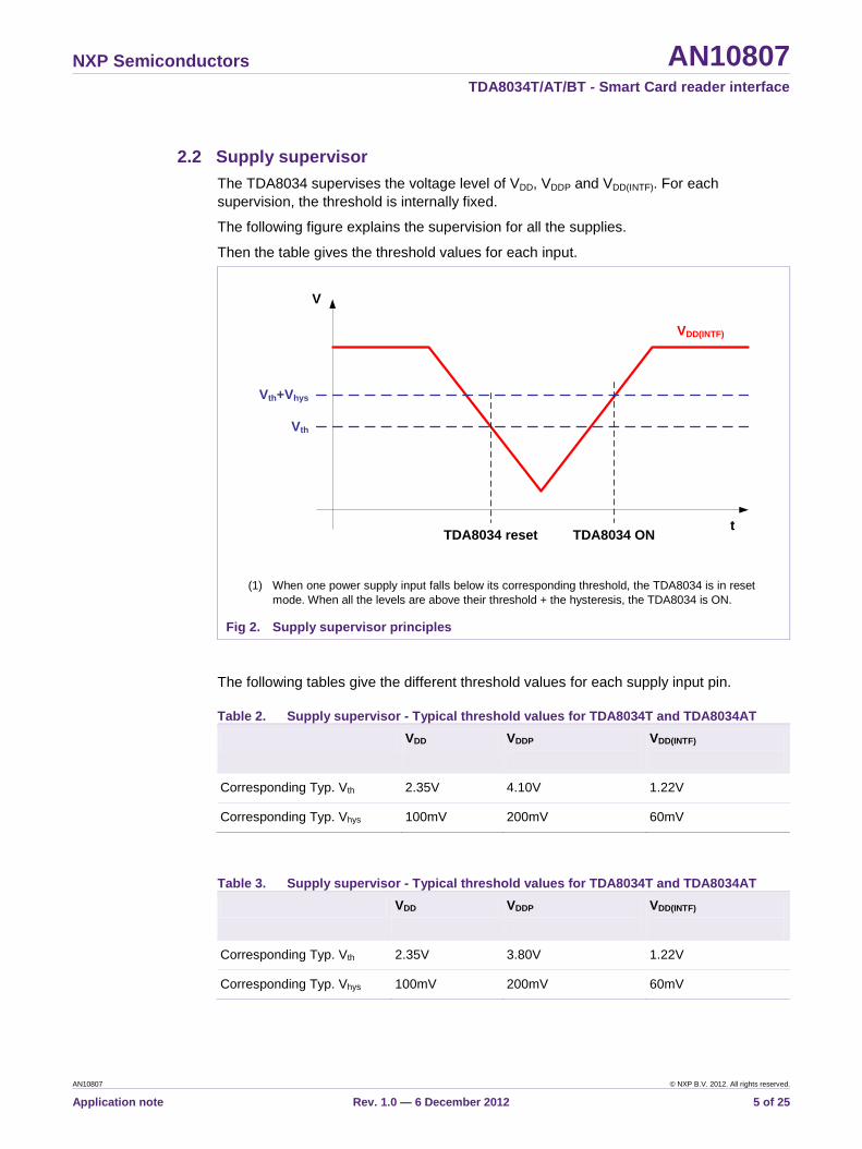
2.2 Supply supervisor The TDA8034 supervises the voltage level of VDD, VDDP and VDD(INTF). For each supervision, the threshold is internally fixed.
The following figure explains the supervision for all the supplies.
Then the table gives the threshold values for each input.
VDD(INTF)
V
t
Vth
TDA8034 reset TDA8034 ON
Vth+Vhys
(1) When one power supply input falls below its corresponding threshold, the TDA8034 is in reset mode. When all the levels are above their threshold + the hysteresis, the TDA8034 is ON.
Fig 2. Supply supervisor principles
The following tables give the different threshold values for each supply input pin.
Table 2. Supply supervisor - Typical threshold values for TDA8034T and TDA8034AT VDD VDDP
VDD(INTF)
Corresponding Typ. Vth 2.35V 4.10V 1.22V
Corresponding Typ. Vhys 100mV 200mV 60mV
Table 3. Supply supervisor - Typical threshold values for TDA8034T and TDA8034AT VDD VDDP
VDD(INTF)
Corresponding Typ. Vth 2.35V 3.80V 1.22V
Corresponding Typ. Vhys 100mV 200mV 60mV
NXP Semiconductors AN10807 TDA8034T/AT/BT - Smart Card reader interface
AN10807 © NXP B.V. 2012. All rights reserved.
Application note Rev. 1.0 — 6 December 2012 6 of 25
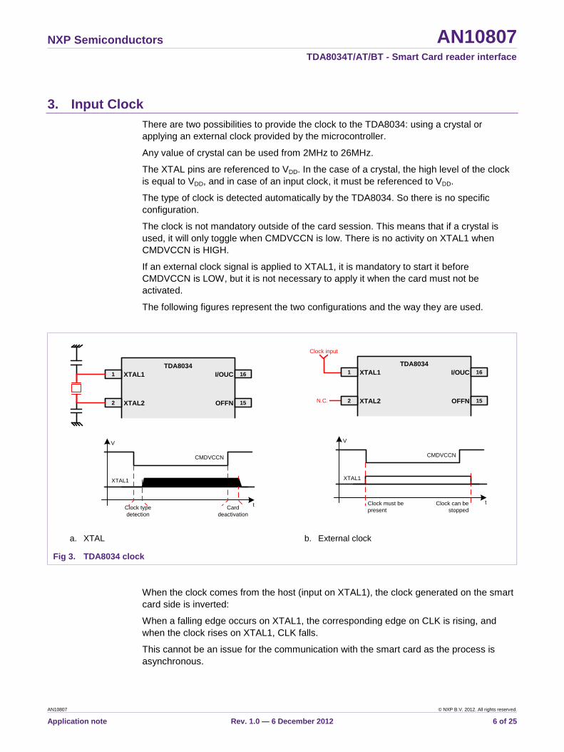
3. Input Clock There are two possibilities to provide the clock to the TDA8034: using a crystal or applying an external clock provided by the microcontroller.
Any value of crystal can be used from 2MHz to 26MHz.
The XTAL pins are referenced to VDD. In the case of a crystal, the high level of the clock is equal to VDD, and in case of an input clock, it must be referenced to VDD.
The type of clock is detected automatically by the TDA8034. So there is no specific configuration.
The clock is not mandatory outside of the card session. This means that if a crystal is used, it will only toggle when CMDVCCN is low. There is no activity on XTAL1 when CMDVCCN is HIGH.
If an external clock signal is applied to XTAL1, it is mandatory to start it before CMDVCCN is LOW, but it is not necessary to apply it when the card must not be activated.
The following figures represent the two configurations and the way they are used.
16
15
1
2
I/OUC
OFFN
XTAL1
XTAL2
Con
fig
16
15
14
121110987
6
5
4 EN1.8VN
CMDVCCN
CLKDIV1
CLK
DIV
2
PRES
N
I/O AU
X1
AU
X2
GN
D
CLK
RST
VCC
CMDVCCN
XTAL1
Clock type detection
Card deactivation
V
t
TDA8034
N.C.
Clock input
16
15
1
2
I/OUC
OFFN
XTAL1
XTAL2
Con
fig16
15
14
121110987
6
5
4 EN1.8VN
CMDVCCN
CLKDIV1
CLK
DIV
2
PRES
N
I/O AU
X1
AU
X2
GN
DCLK
RST
VCC
CMDVCCN
XTAL1
Clock must be present
Clock can be stopped
V
t
TDA8034
a. XTAL b. External clock
Fig 3. TDA8034 clock
When the clock comes from the host (input on XTAL1), the clock generated on the smart card side is inverted:
When a falling edge occurs on XTAL1, the corresponding edge on CLK is rising, and when the clock rises on XTAL1, CLK falls.
This cannot be an issue for the communication with the smart card as the process is asynchronous.
NXP Semiconductors AN10807 TDA8034T/AT/BT - Smart Card reader interface
AN10807 © NXP B.V. 2012. All rights reserved.
Application note Rev. 1.0 — 6 December 2012 7 of 25
4. Card connector
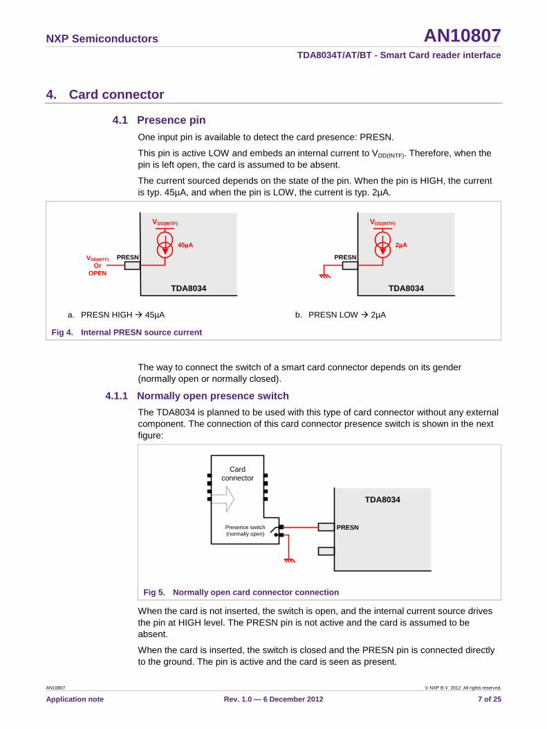
4.1 Presence pin One input pin is available to detect the card presence: PRESN.
This pin is active LOW and embeds an internal current to VDD(INTF). Therefore, when the pin is left open, the card is assumed to be absent.
The current sourced depends on the state of the pin. When the pin is HIGH, the current is typ. 45µA, and when the pin is LOW, the current is typ. 2µA.
TDA8034
PRESNVDD(INTF)Or
OPEN
VDD(INTF)
45µA
TDA8034
PRESN
VDD(INTF)
2µA
a. PRESN HIGH 45µA b. PRESN LOW 2µA
Fig 4. Internal PRESN source current
The way to connect the switch of a smart card connector depends on its gender (normally open or normally closed).
4.1.1 Normally open presence switch The TDA8034 is planned to be used with this type of card connector without any external component. The connection of this card connector presence switch is shown in the next figure:
Card connector
Presence switch(normally open)
TDA8034
PRESN
Fig 5. Normally open card connector connection
When the card is not inserted, the switch is open, and the internal current source drives the pin at HIGH level. The PRESN pin is not active and the card is assumed to be absent.
When the card is inserted, the switch is closed and the PRESN pin is connected directly to the ground. The pin is active and the card is seen as present.
NXP Semiconductors AN10807 TDA8034T/AT/BT - Smart Card reader interface
AN10807 © NXP B.V. 2012. All rights reserved.
Application note Rev. 1.0 — 6 December 2012 8 of 25
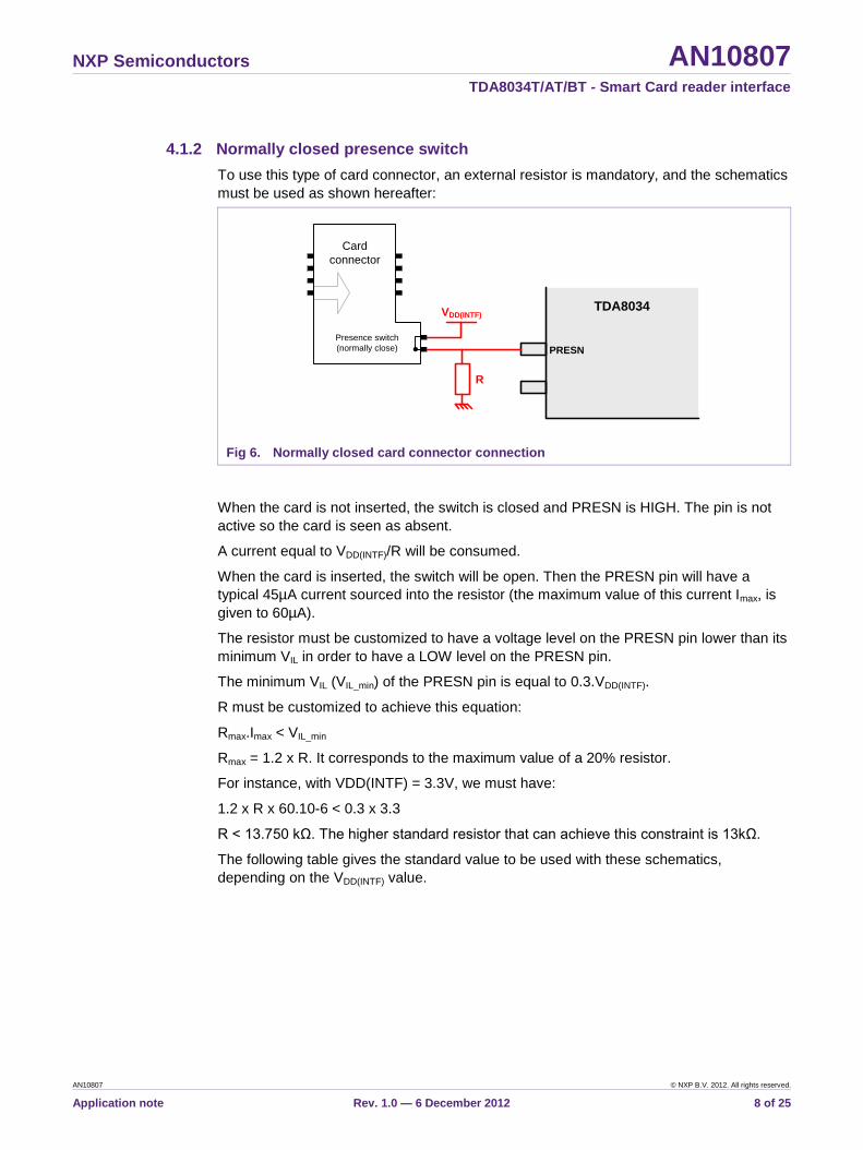
4.1.2 Normally closed presence switch To use this type of card connector, an external resistor is mandatory, and the schematics must be used as shown hereafter:
Card connector
Presence switch(normally close)
TDA8034
PRESN
VDD(INTF)
R
Fig 6. Normally closed card connector connection
When the card is not inserted, the switch is closed and PRESN is HIGH. The pin is not active so the card is seen as absent.
A current equal to VDD(INTF)/R will be consumed.
When the card is inserted, the switch will be open. Then the PRESN pin will have a typical 45µA current sourced into the resistor (the maximum value of this current Imax, is given to 60µA).
The resistor must be customized to have a voltage level on the PRESN pin lower than its minimum VIL in order to have a LOW level on the PRESN pin.
The minimum VIL (VIL_min) of the PRESN pin is equal to 0.3.VDD(INTF).
R must be customized to achieve this equation:
Rmax.Imax < VIL_min
Rmax = 1.2 x R. It corresponds to the maximum value of a 20% resistor.
For instance, with VDD(INTF) = 3.3V, we must have:
1.2 x R x 60.10-6 < 0.3 x 3.3
R < 13.750 kΩ. The higher standard resistor that can achieve this constraint is 13kΩ.
The following table gives the standard value to be used with these schematics, depending on the VDD(INTF) value.
NXP Semiconductors AN10807 TDA8034T/AT/BT - Smart Card reader interface
AN10807 © NXP B.V. 2012. All rights reserved.
Application note Rev. 1.0 — 6 December 2012 9 of 25
Table 4. Pull down resistor wrt VDD(INTF) VDD(INTF) Standardized resistor value
1.6V ≤ VDD(INTF) < 1.8V 6.2kΩ
1.8V ≤ VDD(INTF) < 2V 7.5kΩ
2V ≤ VDD(INTF) < 2.2V 8.2kΩ
2.2V ≤ VDD(INTF) < 2.4V 9.1kΩ
2.4V ≤ VDD(INTF) < 2.7V 10kΩ
2.7V ≤ VDD(INTF) < 2.9V 11kΩ
2.9V ≤ VDD(INTF) < 3.2V 12kΩ
3.2V ≤ VDD(INTF) 13kΩ
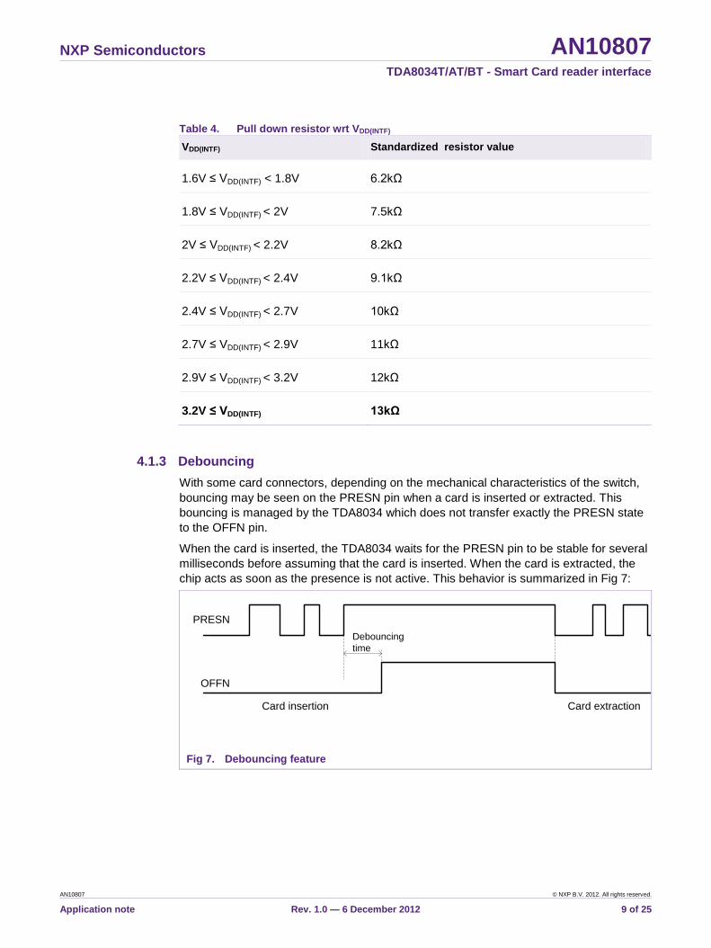
4.1.3 Debouncing With some card connectors, depending on the mechanical characteristics of the switch, bouncing may be seen on the PRESN pin when a card is inserted or extracted. This bouncing is managed by the TDA8034 which does not transfer exactly the PRESN state to the OFFN pin.
When the card is inserted, the TDA8034 waits for the PRESN pin to be stable for several milliseconds before assuming that the card is inserted. When the card is extracted, the chip acts as soon as the presence is not active. This behavior is summarized in Fig 7:
PRESN
OFFN
Debouncing time
Card insertion Card extraction
Fig 7. Debouncing feature
NXP Semiconductors AN10807 TDA8034T/AT/BT - Smart Card reader interface
AN10807 © NXP B.V. 2012. All rights reserved.
Application note Rev. 1.0 — 6 December 2012 10 of 25
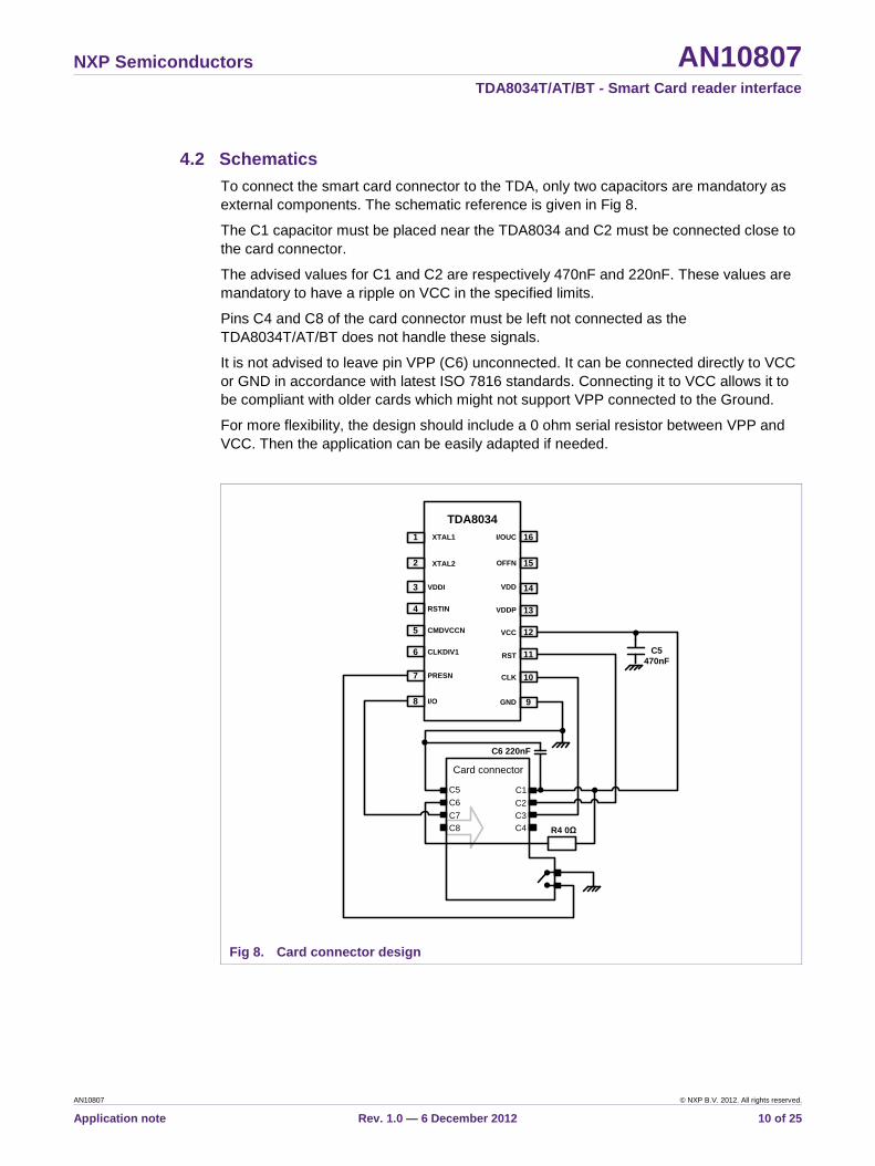
4.2 Schematics To connect the smart card connector to the TDA, only two capacitors are mandatory as external components. The schematic reference is given in Fig 8.
The C1 capacitor must be placed near the TDA8034 and C2 must be connected close to the card connector.
The advised values for C1 and C2 are respectively 470nF and 220nF. These values are mandatory to have a ripple on VCC in the specified limits.
Pins C4 and C8 of the card connector must be left not connected as the TDA8034T/AT/BT does not handle these signals.
It is not advised to leave pin VPP (C6) unconnected. It can be connected directly to VCC or GND in accordance with latest ISO 7816 standards. Connecting it to VCC allows it to be compliant with older cards which might not support VPP connected to the Ground.
For more flexibility, the design should include a 0 ohm serial resistor between VPP and VCC. Then the application can be easily adapted if needed.
Card connector
C5C6C7C8
C1C2C3C4
C6 220nF
R4 0Ω
3 VDDI
4 RSTIN
5 CMDVCCN
6 CLKDIV1
9
10CLK
11RST
12VCC
13VDDP
14VDD
15OFFN
16I/OUC
C5470nF
TDA80341 XTAL1
2 XTAL2
8 I/O
7 PRESN
GND
Fig 8. Card connector design
NXP Semiconductors AN10807 TDA8034T/AT/BT - Smart Card reader interface
AN10807 © NXP B.V. 2012. All rights reserved.
Application note Rev. 1.0 — 6 December 2012 11 of 25
5. Card configuration The chip can be configured dynamically to operate with the connected card. Two parameters can be controlled: the voltage level and the frequency of the clock signal to the card.
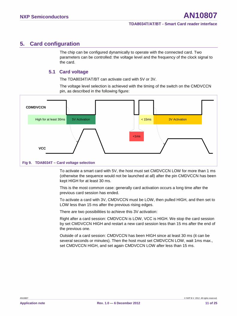
5.1 Card voltage The TDA8034T/AT/BT can activate card with 5V or 3V.
The voltage level selection is achieved with the timing of the switch on the CMDVCCN pin, as described in the following figure:
5V Activation
CDMDVCCN
High for at least 30ms < 15ms 3V Activation
VCC
<1ms
Fig 9. TDA8034T – Card voltage selection
To activate a smart card with 5V, the host must set CMDVCCN LOW for more than 1 ms (otherwise the sequence would not be launched at all) after the pin CMDVCCN has been kept HIGH for at least 30 ms.
This is the most common case: generally card activation occurs a long time after the previous card session has ended.
To activate a card with 3V, CMDVCCN must be LOW, then pulled HIGH, and then set to LOW less than 15 ms after the previous rising edges.
There are two possibilities to achieve this 3V activation:
Right after a card session: CMDVCCN is LOW, VCC is HIGH. We stop the card session by set CMDVCCN HIGH and restart a new card session less than 15 ms after the end of the previous one.
Outside of a card session: CMDVCCN has been HIGH since at least 30 ms (it can be several seconds or minutes). Then the host must set CMDVCCN LOW, wait 1ms max., set CMDVCCN HIGH, and set again CMDVCCN LOW after less than 15 ms.
NXP Semiconductors AN10807 TDA8034T/AT/BT - Smart Card reader interface
AN10807 © NXP B.V. 2012. All rights reserved.
Application note Rev. 1.0 — 6 December 2012 12 of 25
5.2 Card clock 5.2.1 Frequency selection
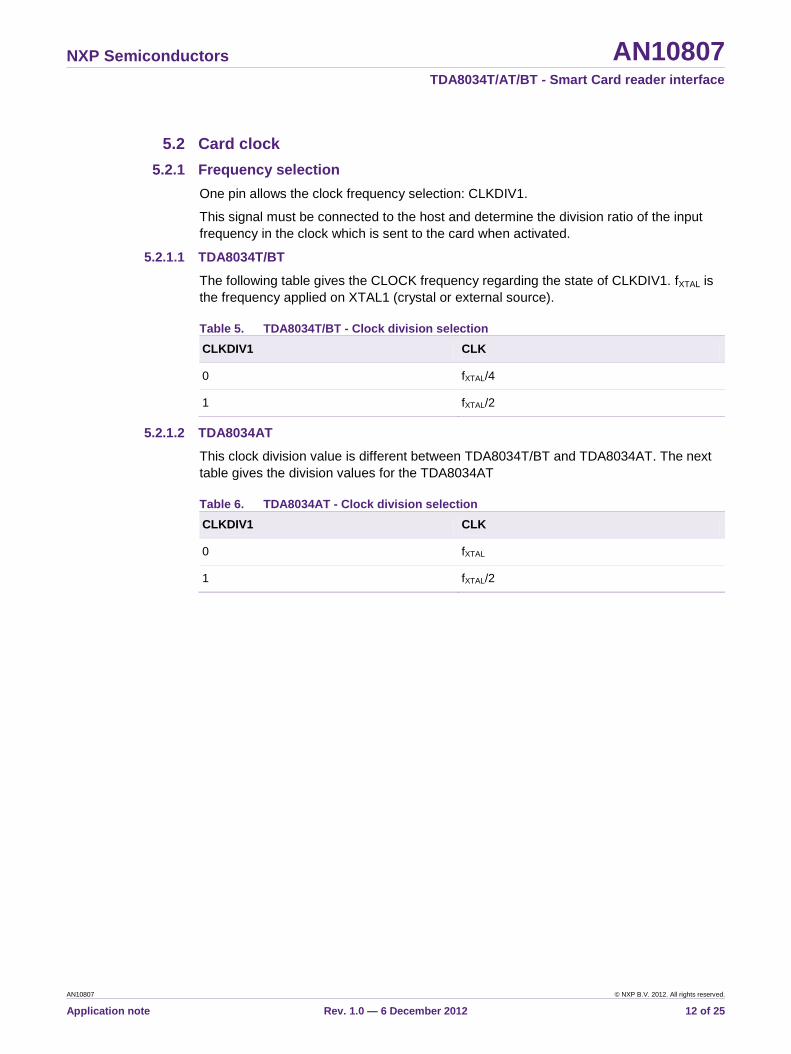
One pin allows the clock frequency selection: CLKDIV1.
This signal must be connected to the host and determine the division ratio of the input frequency in the clock which is sent to the card when activated.
5.2.1.1 TDA8034T/BT
The following table gives the CLOCK frequency regarding the state of CLKDIV1. fXTAL is the frequency applied on XTAL1 (crystal or external source).
Table 5. TDA8034T/BT - Clock division selection CLKDIV1 CLK
0 fXTAL/4
1 fXTAL/2
5.2.1.2 TDA8034AT
This clock division value is different between TDA8034T/BT and TDA8034AT. The next table gives the division values for the TDA8034AT
Table 6. TDA8034AT - Clock division selection CLKDIV1 CLK
0 fXTAL
1 fXTAL/2
NXP Semiconductors AN10807 TDA8034T/AT/BT - Smart Card reader interface
AN10807 © NXP B.V. 2012. All rights reserved.
Application note Rev. 1.0 — 6 December 2012 13 of 25
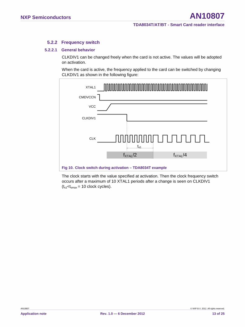
5.2.2 Frequency switch 5.2.2.1 General behavior
CLKDIV1 can be changed freely when the card is not active. The values will be adopted on activation.
When the card is active, the frequency applied to the card can be switched by changing CLKDIV1 as shown in the following figure:
ts1
XTAL1
CMDVCCN
VCC
CLKDIV1
CLK
fXTAL/2 fXTAL/4
Fig 10. Clock switch during activation – TDA8034T example
The clock starts with the value specified at activation. Then the clock frequency switch occurs after a maximum of 10 XTAL1 periods after a change is seen on CLKDIV1 (ts1<tsmax = 10 clock cycles).
NXP Semiconductors AN10807 TDA8034T/AT/BT - Smart Card reader interface
AN10807 © NXP B.V. 2012. All rights reserved.
Application note Rev. 1.0 — 6 December 2012 14 of 25
6. Card Activation / Deactivation
6.1 CMDVCCN behavior Note: a falling edge on CMDVCCN described in the following chapter represents either a simple falling edge of CMDVCCN (for a 5V activation) or a sequence on the pin for a 3V activation.
6.2 Difference TDA8024 – TDA8034 6.2.1 Activation timing
The electrical interface between the host and the TDA is based on GPIOs and is the same for TDA8034 as for TDA8024.
In the card management, two differences exist between the TDA8024 and TDA8034: the voltage selection, using CMDVCCN, as described in chapter 5.1, and the delay between CMDVCCN Low and VCC High.
This delay is very low for the TDA8024 while it is equal to 3.47ms in the TDA8034 (see next chapter).
6.2.2 Software When the TDA8034 is implemented in a design, the software already developed for the TDA8024 can be reused, with the card voltage selection implementation, and another modification in one case:
If, for the TDA8024, the delay between VCC High and RST High had been set to a low value (below 3.5ms), this delay must be changed to a highest value, as described in the next chapter.
If the delay is greater than 3.5ms, then the same code can be reused without any change.
NXP Semiconductors AN10807 TDA8034T/AT/BT - Smart Card reader interface
AN10807 © NXP B.V. 2012. All rights reserved.
Application note Rev. 1.0 — 6 December 2012 15 of 25
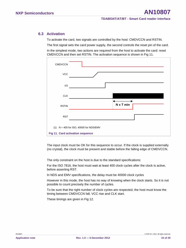
6.3 Activation To activate the card, two signals are controlled by the host: CMDVCCN and RSTIN.
The first signal sets the card power supply, the second controls the reset pin of the card.
In the simplest mode, two actions are required from the host to activate the card: reset CMDVCCN and then set RSTIN. The activation sequence is shown in Fig 11.
CMDVCCN
VCC
I/O
CLK
RSTIN
RST
N x T min
(1) N = 400 for ISO, 40000 for NDS/EMV
Fig 11. Card activation sequence
The input clock must be OK for this sequence to occur. If the clock is supplied externally (no crystal), the clock must be present and stable before the falling edge of CMDVCCN.
The only constraint on the host is due to the standard specifications:
For the ISO 7816, the host must wait at least 400 clock cycles after the clock is active, before asserting RST.
In NDS and EMV specifications, the delay must be 40000 clock cycles
However in this mode, the host has no way of knowing when the clock starts. So it is not possible to count precisely the number of cycles.
To be sure that the right number of clock cycles are respected, the host must know the timing between CMDVCCN fall, VCC rise and CLK start.
These timings are given in Fig 12.
NXP Semiconductors AN10807 TDA8034T/AT/BT - Smart Card reader interface
AN10807 © NXP B.V. 2012. All rights reserved.
Application note Rev. 1.0 — 6 December 2012 16 of 25
CMDVCCN
VCC
I/O
CLK
RSTIN
RST
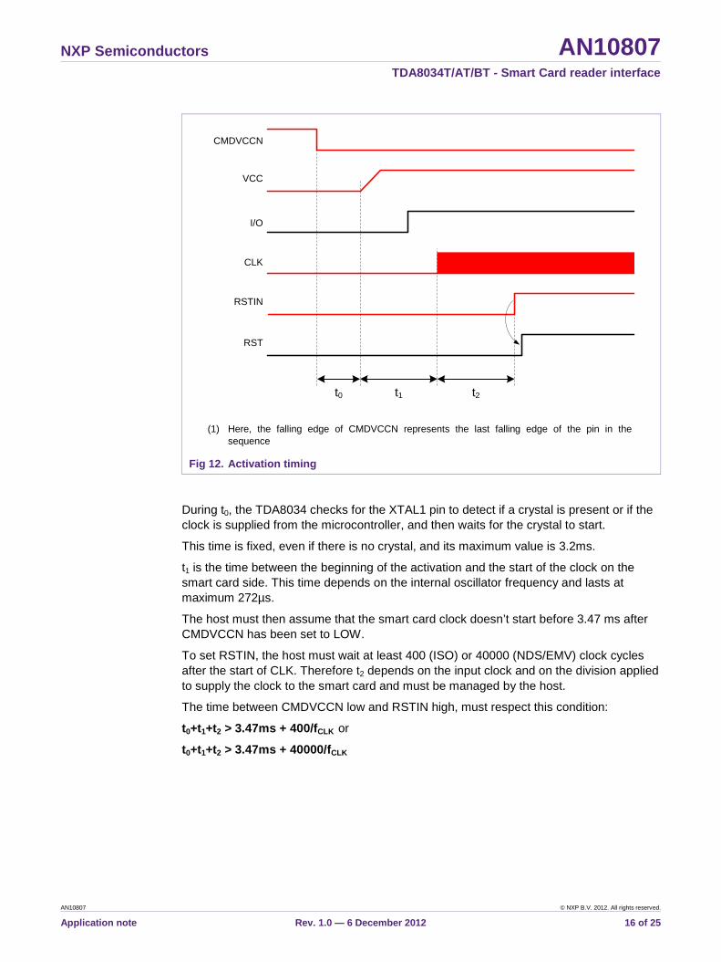
t0 t1 t2
(1) Here, the falling edge of CMDVCCN represents the last falling edge of the pin in the sequence
Fig 12. Activation timing
During t0, the TDA8034 checks for the XTAL1 pin to detect if a crystal is present or if the clock is supplied from the microcontroller, and then waits for the crystal to start.
This time is fixed, even if there is no crystal, and its maximum value is 3.2ms.
t1 is the time between the beginning of the activation and the start of the clock on the smart card side. This time depends on the internal oscillator frequency and lasts at maximum 272µs.
The host must then assume that the smart card clock doesn’t start before 3.47 ms after CMDVCCN has been set to LOW.
To set RSTIN, the host must wait at least 400 (ISO) or 40000 (NDS/EMV) clock cycles after the start of CLK. Therefore t2 depends on the input clock and on the division applied to supply the clock to the smart card and must be managed by the host.
The time between CMDVCCN low and RSTIN high, must respect this condition:
t0+t1+t2 > 3.47ms + 400/fCLK or
t0+t1+t2 > 3.47ms + 40000/fCLK
NXP Semiconductors AN10807 TDA8034T/AT/BT - Smart Card reader interface
AN10807 © NXP B.V. 2012. All rights reserved.
Application note Rev. 1.0 — 6 December 2012 17 of 25
6.4 Deactivation The deactivation is managed entirely by the TDA8034 sequencer. Deactivation occurs when one of the following events happens: • Rising edge of CMDVCCN (normal host deactivation) • A fault is detected:
− Card removal − Overheating − Short-circuit or high current on VCC − VDD(INTF), VDD or VDDP drop
The deactivation sequence is automatic and fully compliant with the standard. For more details on the activation or deactivation sequence and their timings, refer to the TDA8034 data sheet and ISO 7816-3 standard.
7. Card operation
7.1 I/O The TDA8034 acts as a simple transceiver incorporating a voltage level shifting adaptation for these signals, once the card is activated.
As there is no other conversion, the host must manage entirely the protocol defined by ISO 7816 (Baudrate, timing, frame…).
The TDA8034 only limits the current on the pins. There is a limitation of 15mA in both directions. I/O is linked to I/OUC. I/OUC must be connected directly to an I/O of the host.
7.2 Warm reset The host can operate a warm reset with the TDA8034: as the RST card pin is the copy of the RSTIN pin, the host just needs to apply a falling edge on RSTIN, followed by a rising edge, and the card shall send its ATR again.
NXP Semiconductors AN10807 TDA8034T/AT/BT - Smart Card reader interface
AN10807 © NXP B.V. 2012. All rights reserved.
Application note Rev. 1.0 — 6 December 2012 18 of 25
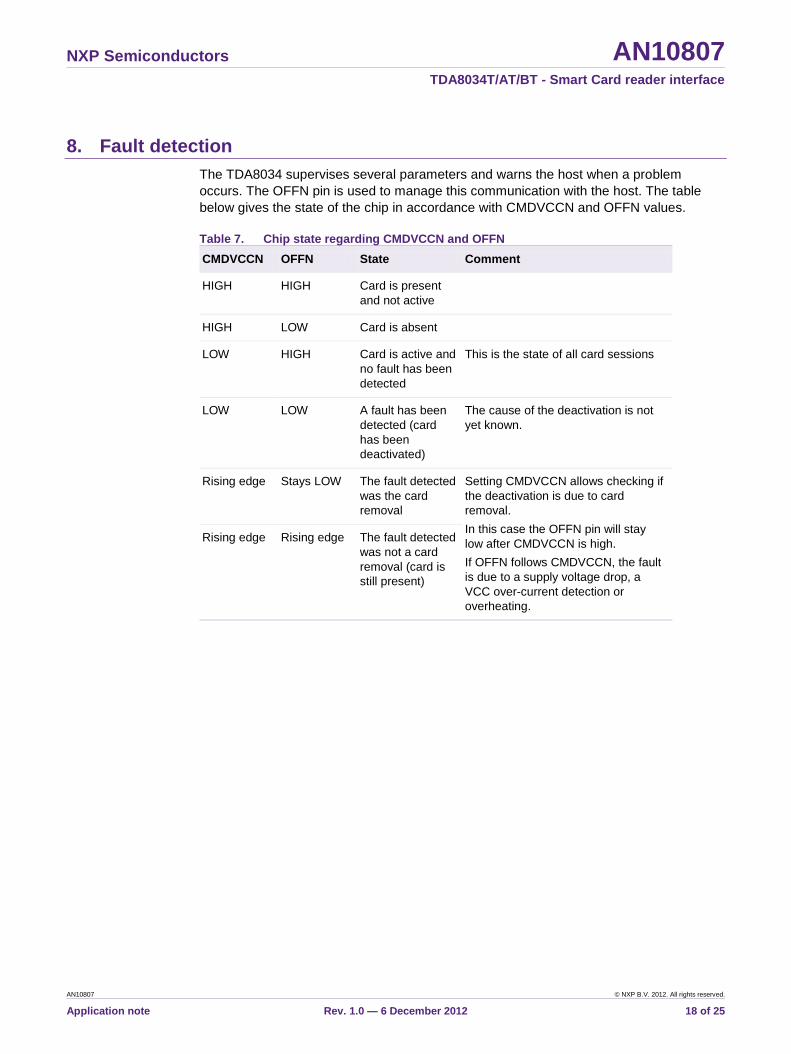
8. Fault detection The TDA8034 supervises several parameters and warns the host when a problem occurs. The OFFN pin is used to manage this communication with the host. The table below gives the state of the chip in accordance with CMDVCCN and OFFN values.
Table 7. Chip state regarding CMDVCCN and OFFN CMDVCCN OFFN State Comment
HIGH HIGH Card is present and not active
HIGH LOW Card is absent
LOW HIGH Card is active and no fault has been detected
This is the state of all card sessions
LOW LOW A fault has been detected (card has been deactivated)
The cause of the deactivation is not yet known.
Rising edge Stays LOW The fault detected was the card removal
Setting CMDVCCN allows checking if the deactivation is due to card removal. In this case the OFFN pin will stay low after CMDVCCN is high. If OFFN follows CMDVCCN, the fault is due to a supply voltage drop, a VCC over-current detection or overheating.
Rising edge Rising edge The fault detected was not a card removal (card is still present)
NXP Semiconductors AN10807 TDA8034T/AT/BT - Smart Card reader interface
AN10807 © NXP B.V. 2012. All rights reserved.
Application note Rev. 1.0 — 6 December 2012 19 of 25
9. Electrical design recommendations
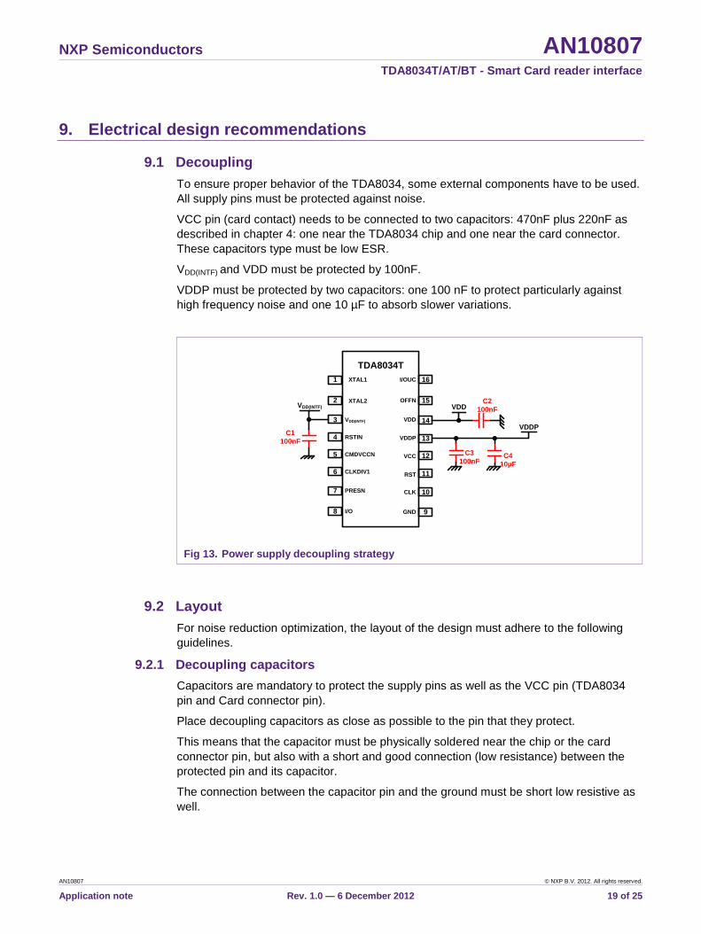
9.1 Decoupling To ensure proper behavior of the TDA8034, some external components have to be used. All supply pins must be protected against noise.
VCC pin (card contact) needs to be connected to two capacitors: 470nF plus 220nF as described in chapter 4: one near the TDA8034 chip and one near the card connector. These capacitors type must be low ESR.
VDD(INTF) and VDD must be protected by 100nF.
VDDP must be protected by two capacitors: one 100 nF to protect particularly against high frequency noise and one 10 µF to absorb slower variations.
3 VDD(INTF)
4 RSTIN
5 CMDVCCN
6 CLKDIV1
9
10CLK
11RST
12VCC
13VDDP
14VDD
15OFFN
16I/OUC
VDD(INTF) VDD
VDDPC1
100nF
C2100nF
C3100nF
TDA8034T1 XTAL1
2 XTAL2
8 I/O
7 PRESN
GND
C410µF
Fig 13. Power supply decoupling strategy
9.2 Layout For noise reduction optimization, the layout of the design must adhere to the following guidelines.
9.2.1 Decoupling capacitors Capacitors are mandatory to protect the supply pins as well as the VCC pin (TDA8034 pin and Card connector pin).
Place decoupling capacitors as close as possible to the pin that they protect.
This means that the capacitor must be physically soldered near the chip or the card connector pin, but also with a short and good connection (low resistance) between the protected pin and its capacitor.
The connection between the capacitor pin and the ground must be short low resistive as well.
NXP Semiconductors AN10807 TDA8034T/AT/BT - Smart Card reader interface
AN10807 © NXP B.V. 2012. All rights reserved.
Application note Rev. 1.0 — 6 December 2012 20 of 25
9.2.2 Clock wires Clock (card) or oscillator signals can cause crosstalk to other signals. It is advised to isolate these signals: make the connections as short as possible and keep them far from other signals.
The best is to shield these signals with ground when possible.
9.2.3 Card ground connection There is no ground pin dedicated to the smart card connector on the TDA8034. Therefore the C5 pin of the card connector must be connected to the main ground layer with a short and low resistive connection.
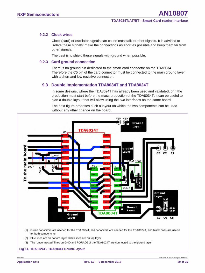
9.3 Double implementation TDA8034T and TDA8024T In some designs, where the TDA8024T has already been used and validated, or if the production must start before the mass production of the TDA8034T, it can be useful to plan a double layout that will allow using the two interfaces on the same board.
The next figure proposes such a layout on which the two components can be used without any other change on the board.
(1) Green capacitors are needed for the TDA8034T, red capacitors are needed for the TDA8024T, and black ones are useful for both components
(2) Blue lines are on bottom layer, black lines are on top layer (3) The “unconnected” lines on GND and PORADJ of the TDA8024T are connected to the ground layer
Fig 14. TDA8024T / TDA8034T Double layout
NXP Semiconductors AN10807 TDA8034T/AT/BT - Smart Card reader interface
AN10807 © NXP B.V. 2012. All rights reserved.
Application note Rev. 1.0 — 6 December 2012 21 of 25
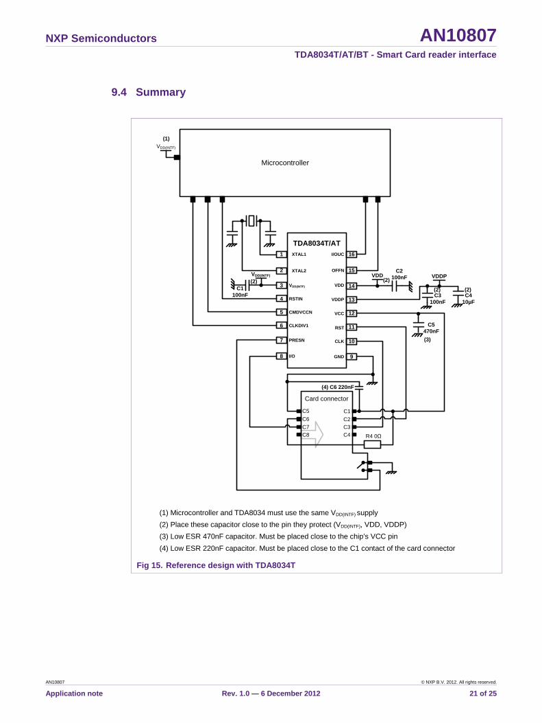
9.4 Summary
Card connector
C5C6C7C8
C1C2C3C4
(4) C6 220nF
R4 0Ω
Microcontroller
VDD(INTF)
(1)
3 VDD(INTF)
4 RSTIN
5 CMDVCCN
6 CLKDIV1
9
10CLK
11RST
12VCC
13VDDP
14VDD
15OFFN
16I/OUC
VDD(INTF) VDD VDDP
C1100nF
C2100nF
C3100nF
C5470nF(3)
(2) (2)
TDA8034T/AT1 XTAL1
2 XTAL2
8 I/O
7 PRESN
(2)
GND
C410µF
(2)
(1) Microcontroller and TDA8034 must use the same VDD(INTF) supply (2) Place these capacitor close to the pin they protect (VDD(INTF), VDD, VDDP) (3) Low ESR 470nF capacitor. Must be placed close to the chip’s VCC pin (4) Low ESR 220nF capacitor. Must be placed close to the C1 contact of the card connector
Fig 15. Reference design with TDA8034T
property nam
e.
Error! Unknow
n document property nam
e. Error! U
nknown docum
ent property
NXP Semiconductors AN10807 TDA8034T/AT/BT - Smart Card reader interface
AN10807 All information provided in this document is subject to legal disclaimers. © NXP B.V. 2012. All rights reserved.
Application note Rev. 1.0 — 6 December 2012 22 of 25
10. Legal information
10.1 Definitions Draft — The document is a draft version only. The content is still under internal review and subject to formal approval, which may result in modifications or additions. NXP Semiconductors does not give any representations or warranties as to the accuracy or completeness of information included herein and shall have no liability for the consequences of use of such information.
10.2 Disclaimers Limited warranty and liability — Information in this document is believed to be accurate and reliable. However, NXP Semiconductors does not give any representations or warranties, expressed or implied, as to the accuracy or completeness of such information and shall have no liability for the consequences of use of such information.
In no event shall NXP Semiconductors be liable for any indirect, incidental, punitive, special or consequential damages (including - without limitation - lost profits, lost savings, business interruption, costs related to the removal or replacement of any products or rework charges) whether or not such damages are based on tort (including negligence), warranty, breach of contract or any other legal theory.
Notwithstanding any damages that customer might incur for any reason whatsoever, NXP Semiconductors’ aggregate and cumulative liability towards customer for the products described herein shall be limited in accordance with the Terms and conditions of commercial sale of NXP Semiconductors.
Right to make changes — NXP Semiconductors reserves the right to make changes to information published in this document, including without limitation specifications and product descriptions, at any time and without notice. This document supersedes and replaces all information supplied prior to the publication hereof.
Suitability for use — NXP Semiconductors products are not designed, authorized or warranted to be suitable for use in life support, life-critical or safety-critical systems or equipment, nor in applications where failure or malfunction of an NXP Semiconductors product can reasonably be expected to result in personal injury, death or severe property or environmental damage. NXP Semiconductors accepts no liability for inclusion and/or use of NXP Semiconductors products in such equipment or applications and therefore such inclusion and/or use is at the customer’s own risk.
Applications — Applications that are described herein for any of these products are for illustrative purposes only. NXP Semiconductors makes no representation or warranty that such applications will be suitable for the specified use without further testing or modification.
Customers are responsible for the design and operation of their applications and products using NXP Semiconductors products, and NXP Semiconductors accepts no liability for any assistance with applications or customer product design. It is customer’s sole responsibility to determine
whether the NXP Semiconductors product is suitable and fit for the customer’s applications and products planned, as well as for the planned application and use of customer’s third party customer(s). Customers should provide appropriate design and operating safeguards to minimize the risks associated with their applications and products.
NXP Semiconductors does not accept any liability related to any default, damage, costs or problem which is based on any weakness or default in the customer’s applications or products, or the application or use by customer’s third party customer(s). Customer is responsible for doing all necessary testing for the customer’s applications and products using NXP Semiconductors products in order to avoid a default of the applications and the products or of the application or use by customer’s third party customer(s). NXP does not accept any liability in this respect.
Export control — This document as well as the item(s) described herein may be subject to export control regulations. Export might require a prior authorization from competent authorities.
Evaluation products — This product is provided on an “as is” and “with all faults” basis for evaluation purposes only. NXP Semiconductors, its affiliates and their suppliers expressly disclaim all warranties, whether express, implied or statutory, including but not limited to the implied warranties of non-infringement, merchantability and fitness for a particular purpose. The entire risk as to the quality, or arising out of the use or performance, of this product remains with customer.
In no event shall NXP Semiconductors, its affiliates or their suppliers be liable to customer for any special, indirect, consequential, punitive or incidental damages (including without limitation damages for loss of business, business interruption, loss of use, loss of data or information, and the like) arising out the use of or inability to use the product, whether or not based on tort (including negligence), strict liability, breach of contract, breach of warranty or any other theory, even if advised of the possibility of such damages.
Notwithstanding any damages that customer might incur for any reason whatsoever (including without limitation, all damages referenced above and all direct or general damages), the entire liability of NXP Semiconductors, its affiliates and their suppliers and customer’s exclusive remedy for all of the foregoing shall be limited to actual damages incurred by customer based on reasonable reliance up to the greater of the amount actually paid by customer for the product or five dollars (US$5.00). The foregoing limitations, exclusions and disclaimers shall apply to the maximum extent permitted by applicable law, even if any remedy fails of its essential purpose.
10.3 Trademarks Notice: All referenced brands, product names, service names and trademarks are property of their respective owners.
NXP Semiconductors AN10807 TDA8034T/AT/BT - Smart Card reader interface
AN10807 All information provided in this document is subject to legal disclaimers. © NXP B.V. 2012. All rights reserved.
Application note Rev. 1.0 — 6 December 2012 23 of 25
11. List of figures
Fig 1. Simplified interfacing view ................................. 3Fig 2. Supply supervisor principles ............................. 5Fig 3. TDA8034 clock .................................................. 6Fig 4. Internal PRESN source current ......................... 7Fig 5. Normally open card connector connection ........ 7Fig 6. Normally closed card connector connection ...... 8Fig 7. Debouncing feature ........................................... 9Fig 8. Card connector design .................................... 10Fig 9. TDA8034T – Card voltage selection ............... 11Fig 10. Clock switch during activation – TDA8034T
example .......................................................... 13Fig 11. Card activation sequence ................................ 15Fig 12. Activation timing .............................................. 16Fig 13. Power supply decoupling strategy .................. 19Fig 14. TDA8024T / TDA8034T Double layout ........... 20Fig 15. Reference design with TDA8034T .................. 21
NXP Semiconductors AN10807 TDA8034T/AT/BT - Smart Card reader interface
AN10807 All information provided in this document is subject to legal disclaimers. © NXP B.V. 2012. All rights reserved.
Application note Rev. 1.0 — 6 December 2012 24 of 25
12. List of tables
Table 1. VDD(INTF) referenced pins ................................... 4Table 2. Supply supervisor - Typical threshold values for
TDA8034T and TDA8034AT ............................. 5Table 3. Supply supervisor - Typical threshold values for
TDA8034T and TDA8034AT ............................. 5Table 4. Pull down resistor wrt VDD(INTF) .......................... 9Table 5. TDA8034T/BT - Clock division selection ......... 12Table 6. TDA8034AT - Clock division selection ............ 12Table 7. Chip state regarding CMDVCCN and OFFN ... 18
NXP Semiconductors AN10807 TDA8034T/AT/BT - Smart Card reader interface
Please be aware that important notices concerning this document and the product(s) described herein, have been included in the section 'Legal information'.
© NXP B.V. 2012. All rights reserved.
For more information, visit: http://www.nxp.com For sales office addresses, please send an email to: [email protected]
Date of release: 6 December 2012 Document identifier: AN10807
13. Contents
1. Introduction ......................................................... 3 1.1 Presentation ....................................................... 3 1.2 Version ............................................................... 3 2. Power supply ....................................................... 4 2.1 Power supply pins .............................................. 4 2.2 Supply supervisor ............................................... 5 3. Input Clock ........................................................... 6 4. Card connector .................................................... 7 4.1 Presence pin ...................................................... 7 4.1.1 Normally open presence switch ......................... 7 4.1.2 Normally closed presence switch ....................... 8 4.1.3 Debouncing ........................................................ 9 4.2 Schematics....................................................... 10 5. Card configuration ............................................ 11 5.1 Card voltage ..................................................... 11 5.2 Card clock ........................................................ 12 5.2.1 Frequency selection ......................................... 12 5.2.1.1 TDA8034T/BT .................................................. 12 5.2.1.2 TDA8034AT ..................................................... 12 5.2.2 Frequency switch ............................................. 13 5.2.2.1 General behavior .............................................. 13 6. Card Activation / Deactivation .......................... 14 6.1 CMDVCCN behavior ........................................ 14 6.2 Difference TDA8024 – TDA8034 ...................... 14 6.2.1 Activation timing ............................................... 14 6.2.2 Software ........................................................... 14 6.3 Activation.......................................................... 15 6.4 Deactivation ..................................................... 17 7. Card operation ................................................... 17 7.1 I/O .................................................................... 17 7.2 Warm reset....................................................... 17 8. Fault detection ................................................... 18 9. Electrical design recommendations ................ 19 9.1 Decoupling ....................................................... 19 9.2 Layout .............................................................. 19 9.2.1 Decoupling capacitors ...................................... 19 9.2.2 Clock wires ....................................................... 20 9.2.3 Card ground connection ................................... 20 9.3 Double implementation TDA8034T and
TDA8024T ........................................................ 20 9.4 Summary .......................................................... 21 10. Legal information .............................................. 22 10.1 Definitions ........................................................ 22 10.2 Disclaimers....................................................... 22
10.3 Trademarks ...................................................... 22 11. List of figures ..................................................... 23 12. List of tables ...................................................... 24 13. Contents ............................................................. 25