Embed Size (px)
Citation preview

AN11228 BGA301x Wideband Variable Gain Amplifier Application Rev. 2 — 3 February 2014 Application note
Document information Info Content Keywords BGA3015, BGA3018, BAP70Q, CATV, Line-up, VGA, Evaluation board
Abstract This application note describes the schematic and layout requirements for using the BGA3015 and BGA3018 drop amplifiers together with the BAP70Q quad pin diode in a CATV VGA application.

NXP Semiconductors AN11228 BGA301x Wideband Variable Gain Amplifier Application
AN11228 All information provided in this document is subject to legal disclaimers. © NXP B.V. 2014. All rights reserved.
Application note Rev. 2 — 3 February 2014 2 of 21
Contact information For more information, please visit: http://www.nxp.com For sales office addresses, please send an email to: [email protected]
Revision history Rev Date Description 2 20140203 Updated with improved application circuit and test data
1 20121012 First version

NXP Semiconductors AN11228 BGA301x Wideband Variable Gain Amplifier Application
AN11228 All information provided in this document is subject to legal disclaimers. © NXP B.V. 2014. All rights reserved.
Application note Rev. 2 — 3 February 2014 3 of 21
1. Introduction With the use of NXP’s BGA301x drop amplifiers and the BAP70Q quad pin diode attenuator a wideband Variable Gain Amplifier (VGA) has been made which can be used as line-up amplifier in CATV networks.
The combination of NXP’s BGA301x amplifiers and BAP70Q pin diode parts a high gain amplifier with low noise figure and wide dynamic range can be made.
This application note describes the evaluation board schematic and layout requirements, and shows the test results.
2. System features • 75 Ω input and output impedance
• Gain control dynamic range of 20 dB
• Flat gain between 40 MHz and 1003 MHz
• Unconditionally stable
• Excellent input and output return loss
3. Customer evaluation kit contents The evaluation kit contains the following items:
• ESD safe casing
• BGA301x VGA evaluation board
NXP Semiconductors AN11228 BGA301x Wideband Variable Gain Amplifier Application
AN11228 All information provided in this document is subject to legal disclaimers. © NXP B.V. 2014. All rights reserved.
Application note Rev. 2 — 3 February 2014 4 of 21
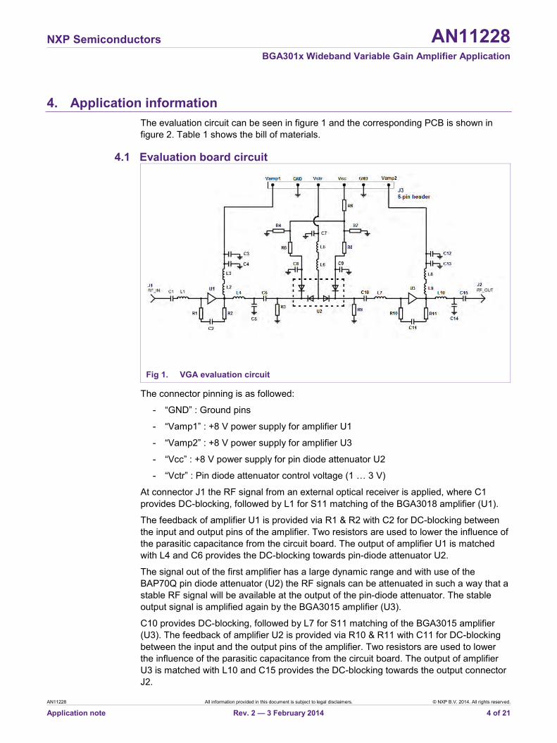
4. Application information The evaluation circuit can be seen in figure 1 and the corresponding PCB is shown in figure 2. Table 1 shows the bill of materials.
4.1 Evaluation board circuit
Fig 1. VGA evaluation circuit
The connector pinning is as followed:
- “GND” : Ground pins
- “Vamp1” : +8 V power supply for amplifier U1
- “Vamp2” : +8 V power supply for amplifier U3
- “Vcc” : +8 V power supply for pin diode attenuator U2
- “Vctr” : Pin diode attenuator control voltage (1 … 3 V)
At connector J1 the RF signal from an external optical receiver is applied, where C1 provides DC-blocking, followed by L1 for S11 matching of the BGA3018 amplifier (U1).
The feedback of amplifier U1 is provided via R1 & R2 with C2 for DC-blocking between the input and output pins of the amplifier. Two resistors are used to lower the influence of the parasitic capacitance from the circuit board. The output of amplifier U1 is matched with L4 and C6 provides the DC-blocking towards pin-diode attenuator U2.
The signal out of the first amplifier has a large dynamic range and with use of the BAP70Q pin diode attenuator (U2) the RF signals can be attenuated in such a way that a stable RF signal will be available at the output of the pin-diode attenuator. The stable output signal is amplified again by the BGA3015 amplifier (U3).
C10 provides DC-blocking, followed by L7 for S11 matching of the BGA3015 amplifier (U3). The feedback of amplifier U2 is provided via R10 & R11 with C11 for DC-blocking between the input and the output pins of the amplifier. Two resistors are used to lower the influence of the parasitic capacitance from the circuit board. The output of amplifier U3 is matched with L10 and C15 provides the DC-blocking towards the output connector J2.
NXP Semiconductors AN11228 BGA301x Wideband Variable Gain Amplifier Application
AN11228 All information provided in this document is subject to legal disclaimers. © NXP B.V. 2014. All rights reserved.
Application note Rev. 2 — 3 February 2014 5 of 21
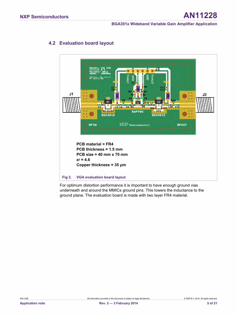
4.2 Evaluation board layout
PCB material = FR4 PCB thickness = 1.5 mm PCB size = 40 mm x 70 mm εr = 4.6 Copper thickness = 35 μm
Fig 2. VGA evaluation board layout
For optimum distortion performance it is important to have enough ground vias underneath and around the MMICs ground pins. This lowers the inductance to the ground plane. The evaluation board is made with two layer FR4 material.
NXP Semiconductors AN11228 BGA301x Wideband Variable Gain Amplifier Application
AN11228 All information provided in this document is subject to legal disclaimers. © NXP B.V. 2014. All rights reserved.
Application note Rev. 2 — 3 February 2014 6 of 21
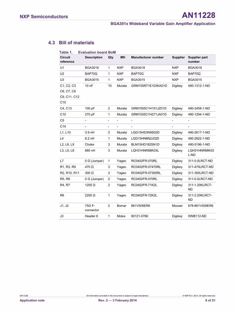
4.3 Bill of materials
Table 1. Evaluation board BoM Circuit reference
Description Qty Mfr Manufacturer number Supplier Supplier part number
U1 BGA3018 1 NXP BGA3018 NXP BGA3018
U2 BAP70Q 1 NXP BAP70Q NXP BAP70Q
U3 BGA3015 1 NXP BGA3015 NXP BGA3015
C1, C2, C3
C6, C7, C8
C9, C11, C12
C15
10 nF 10 Murata GRM155R71E103KA01D Digikey 490-1312-1-ND
C4, C13 100 pF 2 Murata GRM1555C1H101JZ01D Digikey 490-3458-1-ND
C10 270 pF 1 Murata GRM1555C1H271JA01D Digikey 490-1294-1-ND
C5 - - - - - -
C14 - - - - - -
L1, L10 3.9 nH 2 Murata LQG15HS3N9S02D Digikey 490-2617-1-ND
L4 8.2 nH 1 Murata LQG15HN8N2J02D Digikey 490-2622-1-ND
L2, L6, L9 Choke 3 Murata BLM15HD182SN1D Digikey 490-5196-1-ND
L3, L5, L8 880 nH 3 Murata LQH31HNR88K03L Digikey LQH31HNR88K03L-ND
L7 0 Ω (Jumper) 1 Yageo RC0402FR-070RL Digikey 311-0.0LRCT-ND
R1, R3, R9 470 Ω 3 Yageo RC0402FR-07470RL Digikey 311-470LRCT-ND
R2, R10, R11 300 Ω 3 Yageo RC0402FR-07300RL Digikey 311-300LRCT-ND
R5, R8 0 Ω (Jumper) 2 Yageo RC0402FR-070RL Digikey 311-0.0LRCT-ND
R4, R7 1200 Ω 2 Yageo RC0402FR-71K2L Digikey 311-1.20KLRCT-ND
R6 2200 Ω 1 Yageo RC0402FR-72K2L Digikey 311-2.20KLRCT-ND
J1, J2 75Ω F-connector
2 Bomar 861V509ER6 Mouser 678-861V509ER6
J3 Header 6 1 Molex 90121-0766 Digikey WM8112-ND

NXP Semiconductors AN11228 BGA301x Wideband Variable Gain Amplifier Application
AN11228 All information provided in this document is subject to legal disclaimers. © NXP B.V. 2014. All rights reserved.
Application note Rev. 2 — 3 February 2014 7 of 21
5. Measurement results at Vcc = 8 V
5.1 S-Parameters
a. S11: 40 MHz – 1140 MHz
(1): Vctr = 2.13 V (2): Vctr = 1.80 V (3): Vctr = 1.64 V (4): Vctr = 1.50 V (5): Vctr = 1.39 V (6): Vctr = 1.29 V (7): Vctr = 1.12 V
b. S11: 300 kHz – 200 MHz (1): Vctr = 2.13 V (2): Vctr = 1.80 V (3): Vctr = 1.64 V (4): Vctr = 1.50 V (5): Vctr = 1.39 V (6): Vctr = 1.29 V (7): Vctr = 1.12 V
Fig 3. Input matching (S11); Vcc = 8 V
a. S22: 40 MHz – 1140 MHz
(1): Vctr = 2.13 V (2): Vctr = 1.80 V (3): Vctr = 1.64 V (4): Vctr = 1.50 V (5): Vctr = 1.39 V (6): Vctr = 1.29 V (7): Vctr = 1.12 V
b. S22: 300 kHz – 200 MHz
(1): Vctr = 2.13 V (2): Vctr = 1.80 V (3): Vctr = 1.64 V (4): Vctr = 1.50 V (5): Vctr = 1.39 V (6): Vctr = 1.29 V (7): Vctr = 1.12 V
Fig 4. Output matching (S22); Vcc = 8 V

NXP Semiconductors AN11228 BGA301x Wideband Variable Gain Amplifier Application
AN11228 All information provided in this document is subject to legal disclaimers. © NXP B.V. 2014. All rights reserved.
Application note Rev. 2 — 3 February 2014 8 of 21
a. S21: 40 MHz – 1140 MHz
(1): Vctr = 2.13 V (2): Vctr = 1.80 V (3): Vctr = 1.64 V (4): Vctr = 1.50 V (5): Vctr = 1.39 V (6): Vctr = 1.29 V (7): Vctr = 1.12 V
b. S21: 300 kHz – 200 MHz
(1): Vctr = 2.13 V (2): Vctr = 1.80 V (3): Vctr = 1.64 V (4): Vctr = 1.50 V (5): Vctr = 1.39 V (6): Vctr = 1.29 V (7): Vctr = 1.12 V
Fig 5. Gain (S21); Vcc = 8 V
a. K-factor: 40 MHz – 1140 MHz
(1): Vctr = 2.13 V (2): Vctr = 1.80 V (3): Vctr = 1.64 V (4): Vctr = 1.50 V (5): Vctr = 1.39 V (6): Vctr = 1.29 V (7): Vctr = 1.12 V
b. K-factor: 300 kHz – 200 MHz (1): Vctr = 2.13 V (2): Vctr = 1.80 V (3): Vctr = 1.64 V (4): Vctr = 1.50 V (5): Vctr = 1.39 V (6): Vctr = 1.29 (7): Vctr = 1.12 V
Fig 6. K-factor; typical; Vcc = 8 V

NXP Semiconductors AN11228 BGA301x Wideband Variable Gain Amplifier Application
AN11228 All information provided in this document is subject to legal disclaimers. © NXP B.V. 2014. All rights reserved.
Application note Rev. 2 — 3 February 2014 9 of 21
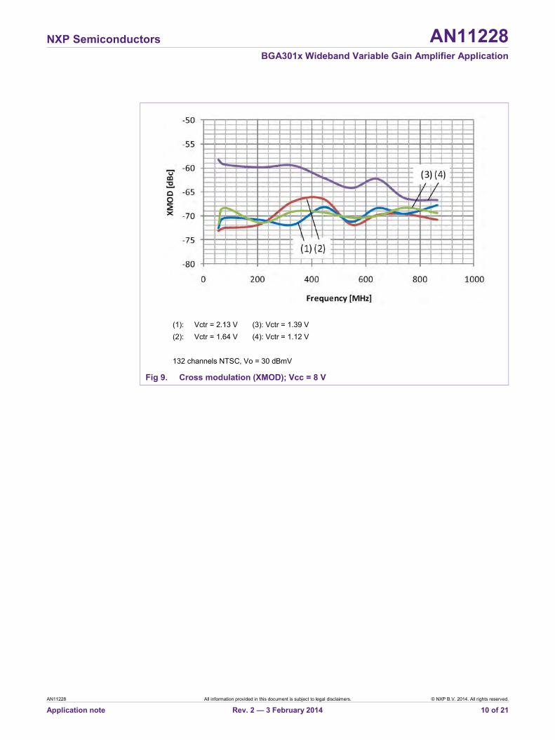
5.2 Distortion
(1): Vctr = 2.13 V (3): Vctr = 1.39 V (2): Vctr = 1.64 V (4): Vctr = 1.12 V
132 channels NTSC, Vo = 30 dBmV
Fig 7. Composite triple beat (CTB); Vcc = 8 V
(1): Vctr = 2.13 V (3): Vctr = 1.39 V (2): Vctr = 1.64 V (4): Vctr = 1.12 V 132 channels NTSC, Vo = 30 dBmV
Fig 8. Composite second order (CSO); Vcc = 8 V
NXP Semiconductors AN11228 BGA301x Wideband Variable Gain Amplifier Application
AN11228 All information provided in this document is subject to legal disclaimers. © NXP B.V. 2014. All rights reserved.
Application note Rev. 2 — 3 February 2014 10 of 21
(1): Vctr = 2.13 V (3): Vctr = 1.39 V (2): Vctr = 1.64 V (4): Vctr = 1.12 V 132 channels NTSC, Vo = 30 dBmV
Fig 9. Cross modulation (XMOD); Vcc = 8 V

NXP Semiconductors AN11228 BGA301x Wideband Variable Gain Amplifier Application
AN11228 All information provided in this document is subject to legal disclaimers. © NXP B.V. 2014. All rights reserved.
Application note Rev. 2 — 3 February 2014 11 of 21
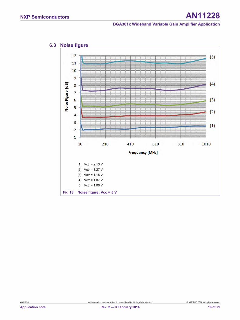
5.3 Noise figure
(1): Vctr = 2.13 V (5): Vctr = 1.39 V (2): Vctr = 1.80 V (6): Vctr = 1.29 V (3): Vctr = 1.64 V (7): Vctr = 1.12 V (4): Vctr = 1.50 V
Fig 10. Noise figure; Vcc = 8 V
NXP Semiconductors AN11228 BGA301x Wideband Variable Gain Amplifier Application
AN11228 All information provided in this document is subject to legal disclaimers. © NXP B.V. 2014. All rights reserved.
Application note Rev. 2 — 3 February 2014 12 of 21
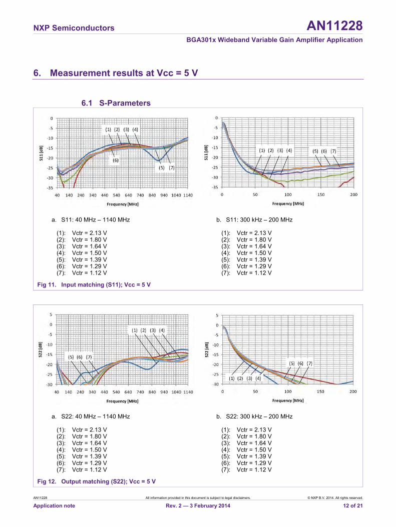
6. Measurement results at Vcc = 5 V
6.1 S-Parameters
a. S11: 40 MHz – 1140 MHz (1): Vctr = 2.13 V (2): Vctr = 1.80 V (3): Vctr = 1.64 V (4): Vctr = 1.50 V (5): Vctr = 1.39 V (6): Vctr = 1.29 V (7): Vctr = 1.12 V
b. S11: 300 kHz – 200 MHz (1): Vctr = 2.13 V (2): Vctr = 1.80 V (3): Vctr = 1.64 V (4): Vctr = 1.50 V (5): Vctr = 1.39 V (6): Vctr = 1.29 V (7): Vctr = 1.12 V
Fig 11. Input matching (S11); Vcc = 5 V
a. S22: 40 MHz – 1140 MHz (1): Vctr = 2.13 V (2): Vctr = 1.80 V (3): Vctr = 1.64 V (4): Vctr = 1.50 V (5): Vctr = 1.39 V (6): Vctr = 1.29 V (7): Vctr = 1.12 V
b. S22: 300 kHz – 200 MHz (1): Vctr = 2.13 V (2): Vctr = 1.80 V (3): Vctr = 1.64 V (4): Vctr = 1.50 V (5): Vctr = 1.39 V (6): Vctr = 1.29 V (7): Vctr = 1.12 V
Fig 12. Output matching (S22); Vcc = 5 V
NXP Semiconductors AN11228 BGA301x Wideband Variable Gain Amplifier Application
AN11228 All information provided in this document is subject to legal disclaimers. © NXP B.V. 2014. All rights reserved.
Application note Rev. 2 — 3 February 2014 13 of 21
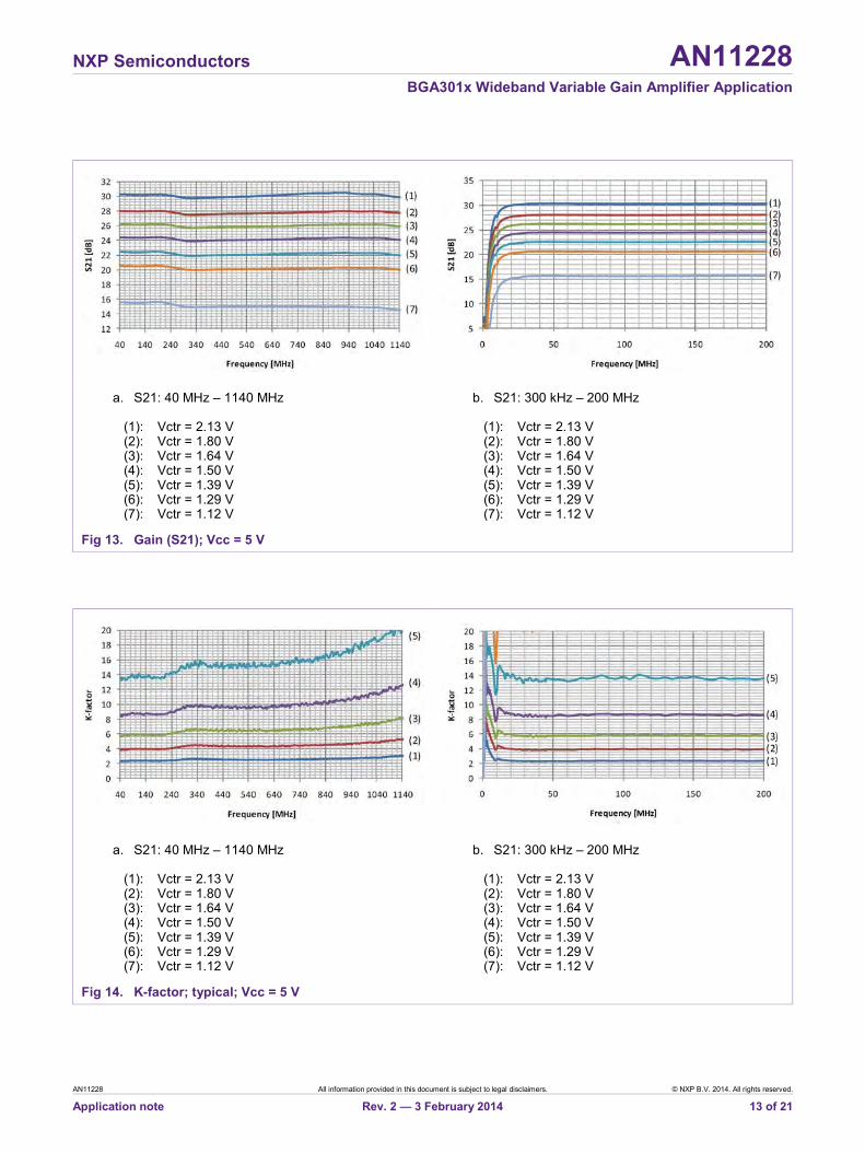
a. S21: 40 MHz – 1140 MHz (1): Vctr = 2.13 V (2): Vctr = 1.80 V (3): Vctr = 1.64 V (4): Vctr = 1.50 V (5): Vctr = 1.39 V (6): Vctr = 1.29 V (7): Vctr = 1.12 V
b. S21: 300 kHz – 200 MHz (1): Vctr = 2.13 V (2): Vctr = 1.80 V (3): Vctr = 1.64 V (4): Vctr = 1.50 V (5): Vctr = 1.39 V (6): Vctr = 1.29 V (7): Vctr = 1.12 V
Fig 13. Gain (S21); Vcc = 5 V
a. S21: 40 MHz – 1140 MHz (1): Vctr = 2.13 V (2): Vctr = 1.80 V (3): Vctr = 1.64 V (4): Vctr = 1.50 V (5): Vctr = 1.39 V (6): Vctr = 1.29 V (7): Vctr = 1.12 V
b. S21: 300 kHz – 200 MHz
(1): Vctr = 2.13 V (2): Vctr = 1.80 V (3): Vctr = 1.64 V (4): Vctr = 1.50 V (5): Vctr = 1.39 V (6): Vctr = 1.29 V (7): Vctr = 1.12 V
Fig 14. K-factor; typical; Vcc = 5 V
NXP Semiconductors AN11228 BGA301x Wideband Variable Gain Amplifier Application
AN11228 All information provided in this document is subject to legal disclaimers. © NXP B.V. 2014. All rights reserved.
Application note Rev. 2 — 3 February 2014 14 of 21
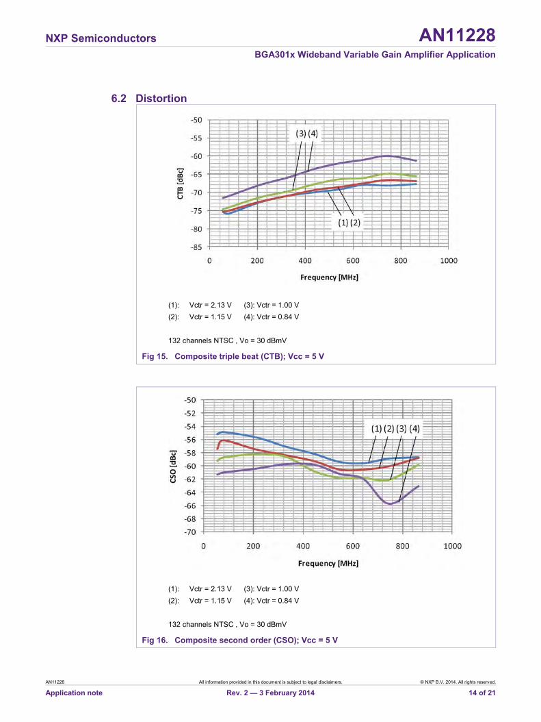
6.2 Distortion
(1): Vctr = 2.13 V (3): Vctr = 1.00 V (2): Vctr = 1.15 V (4): Vctr = 0.84 V 132 channels NTSC , Vo = 30 dBmV
Fig 15. Composite triple beat (CTB); Vcc = 5 V
(1): Vctr = 2.13 V (3): Vctr = 1.00 V (2): Vctr = 1.15 V (4): Vctr = 0.84 V 132 channels NTSC , Vo = 30 dBmV
Fig 16. Composite second order (CSO); Vcc = 5 V
NXP Semiconductors AN11228 BGA301x Wideband Variable Gain Amplifier Application
AN11228 All information provided in this document is subject to legal disclaimers. © NXP B.V. 2014. All rights reserved.
Application note Rev. 2 — 3 February 2014 15 of 21
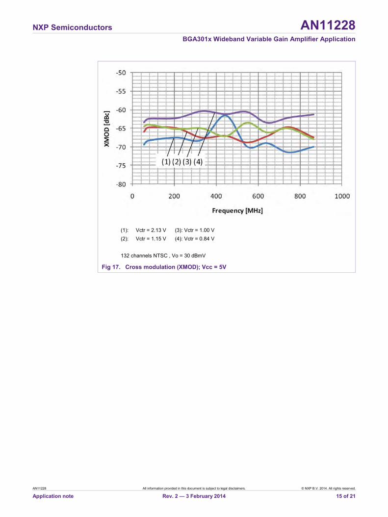
(1): Vctr = 2.13 V (3): Vctr = 1.00 V (2): Vctr = 1.15 V (4): Vctr = 0.84 V 132 channels NTSC , Vo = 30 dBmV
Fig 17. Cross modulation (XMOD); Vcc = 5V
NXP Semiconductors AN11228 BGA301x Wideband Variable Gain Amplifier Application
AN11228 All information provided in this document is subject to legal disclaimers. © NXP B.V. 2014. All rights reserved.
Application note Rev. 2 — 3 February 2014 16 of 21
6.3 Noise figure
(1): Vctr = 2.13 V (2): Vctr = 1.27 V (3): Vctr = 1.15 V (4): Vctr = 1.07 V (5): Vctr = 1.00 V
Fig 18. Noise figure; Vcc = 5 V
NXP Semiconductors AN11228 BGA301x Wideband Variable Gain Amplifier Application
AN11228 All information provided in this document is subject to legal disclaimers. © NXP B.V. 2014. All rights reserved.
Application note Rev. 2 — 3 February 2014 17 of 21
7. Abbreviations
Table 2. Abbreviations Acronym Description AC Alternating Current
CATV Community Antenna Television
DC Direct Current
ESD Electro Static Discharge
MMIC Monolithic Microwave Integrated Circuit
PCB Printed Circuit Board
RF Radio Frequency
SMD Surface Mounted Device
NXP Semiconductors AN11228 BGA301x Wideband Variable Gain Amplifier Application
AN11228 All information provided in this document is subject to legal disclaimers. © NXP B.V. 2014. All rights reserved.
Application note Rev. 2 — 3 February 2014 18 of 21
8. Legal information
8.1 Definitions Draft — The document is a draft version only. The content is still under internal review and subject to formal approval, which may result in modifications or additions. NXP Semiconductors does not give any representations or warranties as to the accuracy or completeness of information included herein and shall have no liability for the consequences of use of such information.
8.2 Disclaimers Limited warranty and liability — Information in this document is believed to be accurate and reliable. However, NXP Semiconductors does not give any representations or warranties, expressed or implied, as to the accuracy or completeness of such information and shall have no liability for the consequences of use of such information.
In no event shall NXP Semiconductors be liable for any indirect, incidental, punitive, special or consequential damages (including - without limitation - lost profits, lost savings, business interruption, costs related to the removal or replacement of any products or rework charges) whether or not such damages are based on tort (including negligence), warranty, breach of contract or any other legal theory.
Notwithstanding any damages that customer might incur for any reason whatsoever, NXP Semiconductors’ aggregate and cumulative liability towards customer for the products described herein shall be limited in accordance with the Terms and conditions of commercial sale of NXP Semiconductors.
Right to make changes — NXP Semiconductors reserves the right to make changes to information published in this document, including without limitation specifications and product descriptions, at any time and without notice. This document supersedes and replaces all information supplied prior to the publication hereof.
Suitability for use — NXP Semiconductors products are not designed, authorized or warranted to be suitable for use in life support, life-critical or safety-critical systems or equipment, nor in applications where failure or malfunction of an NXP Semiconductors product can reasonably be expected to result in personal injury, death or severe property or environmental damage. NXP Semiconductors accepts no liability for inclusion and/or use of NXP Semiconductors products in such equipment or applications and therefore such inclusion and/or use is at the customer’s own risk.
Applications — Applications that are described herein for any of these products are for illustrative purposes only. NXP Semiconductors makes no representation or warranty that such applications will be suitable for the specified use without further testing or modification.
Customers are responsible for the design and operation of their applications and products using NXP Semiconductors products, and NXP Semiconductors accepts no liability for any assistance with applications or
customer product design. It is customer’s sole responsibility to determine whether the NXP Semiconductors product is suitable and fit for the customer’s applications and products planned, as well as for the planned application and use of customer’s third party customer(s). Customers should provide appropriate design and operating safeguards to minimize the risks associated with their applications and products.
NXP Semiconductors does not accept any liability related to any default, damage, costs or problem which is based on any weakness or default in the customer’s applications or products, or the application or use by customer’s third party customer(s). Customer is responsible for doing all necessary testing for the customer’s applications and products using NXP Semiconductors products in order to avoid a default of the applications and the products or of the application or use by customer’s third party customer(s). NXP does not accept any liability in this respect.
Export control — This document as well as the item(s) described herein may be subject to export control regulations. Export might require a prior authorization from national authorities.
Evaluation products — This product is provided on an “as is” and “with all faults” basis for evaluation purposes only. NXP Semiconductors, its affiliates and their suppliers expressly disclaim all warranties, whether express, implied or statutory, including but not limited to the implied warranties of non-infringement, merchantability and fitness for a particular purpose. The entire risk as to the quality, or arising out of the use or performance, of this product remains with customer.
In no event shall NXP Semiconductors, its affiliates or their suppliers be liable to customer for any special, indirect, consequential, punitive or incidental damages (including without limitation damages for loss of business, business interruption, loss of use, loss of data or information, and the like) arising out the use of or inability to use the product, whether or not based on tort (including negligence), strict liability, breach of contract, breach of warranty or any other theory, even if advised of the possibility of such damages.
Notwithstanding any damages that customer might incur for any reason whatsoever (including without limitation, all damages referenced above and all direct or general damages), the entire liability of NXP Semiconductors, its affiliates and their suppliers and customer’s exclusive remedy for all of the foregoing shall be limited to actual damages incurred by customer based on reasonable reliance up to the greater of the amount actually paid by customer for the product or five dollars (US$5.00). The foregoing limitations, exclusions and disclaimers shall apply to the maximum extent permitted by applicable law, even if any remedy fails of its essential purpose.
8.3 Trademarks Notice: All referenced brands, product names, service names and trademarks are property of their respective owners.
NXP Semiconductors AN11228 BGA301x Wideband Variable Gain Amplifier Application
AN11228 All information provided in this document is subject to legal disclaimers. © NXP B.V. 2014. All rights reserved.
Application note Rev. 2 — 3 February 2014 19 of 21
9. List of figures
Fig 1. VGA evaluation circuit ....................................... 4 Fig 2. VGA evaluation board layout ............................ 5 Fig 3. Input matching (S11); Vcc = 8 V ....................... 7 Fig 4. Output matching (S22); Vcc = 8 V .................... 7 Fig 5. Gain (S21); Vcc = 8 V ....................................... 8 Fig 6. K-factor; typical; Vcc = 8 V ................................ 8 Fig 7. Composite triple beat (CTB); Vcc = 8 V ............ 9 Fig 8. Composite second order (CSO); Vcc = 8 V ...... 9 Fig 9. Cross modulation (XMOD); Vcc = 8 V............. 10 Fig 10. Noise figure; Vcc = 8 V ................................... 11 Fig 11. Input matching (S11); Vcc = 5 V ..................... 12 Fig 12. Output matching (S22); Vcc = 5 V .................. 12 Fig 13. Gain (S21); Vcc = 5 V ..................................... 13 Fig 14. K-factor; typical; Vcc = 5 V .............................. 13 Fig 15. Composite triple beat (CTB); Vcc = 5 V .......... 14 Fig 16. Composite second order (CSO); Vcc = 5 V .... 14 Fig 17. Cross modulation (XMOD); Vcc = 5V.............. 15 Fig 18. Noise figure; Vcc = 5 V ................................... 16

NXP Semiconductors AN11228 BGA301x Wideband Variable Gain Amplifier Application
AN11228 All information provided in this document is subject to legal disclaimers. © NXP B.V. 2014. All rights reserved.
Application note Rev. 2 — 3 February 2014 20 of 21
10. List of tables
Table 1. Evaluation board BoM ....................................... 6 Table 2. Abbreviations .................................................. 17
NXP Semiconductors AN11228 BGA301x Wideband Variable Gain Amplifier Application
Please be aware that important notices concerning this document and the product(s) described herein, have been included in the section 'Legal information'.
© NXP B.V. 2014. All rights reserved.
For more information, visit: http://www.nxp.com For sales office addresses, please send an email to: [email protected]
Date of release: 3 February 2014 Document identifier: AN11228
11. Contents
1. Introduction ......................................................... 3 2. System features ................................................... 3 3. Customer evaluation kit contents ...................... 3 4. Application information ...................................... 4 4.1 Evaluation board circuit ...................................... 4 4.2 Evaluation board layout ...................................... 5 4.3 Bill of materials ................................................... 6 5. Measurement results at Vcc = 8 V...................... 7 5.1 S-Parameters ..................................................... 7 5.2 Distortion ............................................................ 9 5.3 Noise figure ...................................................... 11 6. Measurement results at Vcc = 5 V.................... 12 6.1 S-Parameters ................................................... 12 6.2 Distortion .......................................................... 14 6.3 Noise figure ...................................................... 16 7. Abbreviations .................................................... 17 8. Legal information .............................................. 18 8.1 Definitions ........................................................ 18 8.2 Disclaimers....................................................... 18 8.3 Trademarks ...................................................... 18 9. List of figures ..................................................... 19 10. List of tables ...................................................... 20 11. Contents ............................................................. 21


![BGU6101 Wideband silicon low-noise amplifier MMIC · Wideband silicon low-noise amplifier MMIC 7. Static characteristics Table 7. Static characteristics [1] ICC(tot) = ICC + IRF_OUT](https://img.pdfslide.net/doc/110x75/5f8bbe3820a0400a6155b583/bgu6101-wideband-silicon-low-noise-amplifier-mmic-wideband-silicon-low-noise-amplifier.jpg)