Embed Size (px)
Citation preview

AN11742 Dynamic Power Control Rev. 1.4 — 3 December 2016 345514
Application note COMPANY PUBLIC
Document information Info Content Keywords PN5180, PN7462, DPC, Dynamic Power Control, TX Shaping, PCD
Shaping, Automatic Waveshape Control, AWC
Abstract This document describes the Dynamic Power Control (DPC) feature of the PN5180 and the PN7462 and how to use it. It describes how to control the wave shapes using the TX Shaping feature in combination with the DPC. It shows examples with the PNEV5180B and the NFC Cockpit.

NXP Semiconductors AN11742 PN5180 and PN7462 DPC Calibration and Trimming
AN11742 All information provided in this document is subject to legal disclaimers. © NXP Semiconductors N.V. 2016. All rights reserved.
Application note COMPANY PUBLIC
Rev. 1.4 — 3 December 2016 345514
2 of 57
Contact information For more information, please visit: http://www.nxp.com
Revision history Rev Date Description 1.4 20161203 References to PN7462 added
Descriptive title changed Typo in Table 6 corrected
1.3 20160104 Typo in section 2 corrected.
1.2 20151216 Section 4.8 added.
1.1 20151126 Minor update
1.0 20151124 First release

NXP Semiconductors AN11742 PN5180 and PN7462 DPC Calibration and Trimming
AN11742 All information provided in this document is subject to legal disclaimers. © NXP Semiconductors N.V. 2016. All rights reserved.
Application note COMPANY PUBLIC
Rev. 1.4 — 3 December 2016 345514
3 of 57
1. Introduction The Dynamic Power Control (DPC) is a feature of the P5180 and PN7462 that allows to control the transmitter current and therefore the field strength depending on loading and detuning conditions. The DPC can be enabled and then dynamically adapts the output power neither requiring any additional resource on the host µC nor requiring additional components.
Together with the proper DPC antenna tuning (as described in [2]) the DPC offers an improved RF performance. On one hand the overall Q factor of the antenna coil circuitry can be increased. On the other hand the DPC antenna tuning provides an improved transfer function. So the DPC as such can be used to extend the read range or to use smaller antennas, without exceeding the driver current specification of the NFC Reader IC, and without exceeding the maximum field strength limits as given by the ISO/IEC 14443, NFC or EMVCo standards.
The requirement for a proper function is a DPC antenna tuning according to the given guidelines (refer to [2]) and a calibration of the DPC itself.
This calibration must be done per antenna design. It requires to check and ensure the correlation of AGC and ITVDD (as described in section 2) as well as the proper setup of the PN5180 and PN7462 EEPROM (as described in section 3).
Note: Only with a proper DPC calibration the function can be guaranteed and it can be guaranteed that the PN5180 or PN7462 is operated within its specification, when using a DPC antenna tuning:
DPC calibration is a must, when using a DPC antenna tuning!
A DPC trimming procedure allows the compensation of production tolerances. The trimming must be done per device.
The PN5180 and PN7462 offer a TX Shaping feature, which can be used to optimize the pulse shapes (envelope) of the transmitted data per protocol (and bit rate). The TX Shaping in combination with the DPC even allows an automatic adaptation of the pulse shapes due to different loading and detuning conditions, which is called Automatic Waveshape Control (AWC).
This document describes the DPC functionality as such, as well as the calibration and trimming steps. It explains, how to adjust the TX Shaping in combination with the DPC.
The NFC Cockpit (graphical user interface software), which can be used together with the PN5180 evaluation board (PNEV5180B) or PN7462 evaluation board (PNEV7462B), gives a full access to all required functions and allows an easy DPC calibration and optimization. The board is prepared to connect an own antenna. Then the NFC Cockpit can be used to calibrate the DPC and even optimize other PN5180 or PN7462 settings. All the settings can be stored in the PN5180 or PN7462 EEPROM.
The complete EEPROM content can be “dumped” from the PN5180 or PN7462 into an XML file. This XML file can be uploaded again into the PN5180 (resp. PN7462) EEPROM either with the evaluation board and the NFC Cockpit or it can be used to be programmed into the final reader product. This allows a quick and convenient calibration and optimization without a specific test SW. The application SW (e.g. EMVCo L1 stack) is completely independent from the analog settings.

NXP Semiconductors AN11742 PN5180 and PN7462 DPC Calibration and Trimming
AN11742 All information provided in this document is subject to legal disclaimers. © NXP Semiconductors N.V. 2016. All rights reserved.
Application note COMPANY PUBLIC
Rev. 1.4 — 3 December 2016 345514
4 of 57
In case of PN7462 the EEPROM content is part of the firmware build, but still can be handled separately from the code.
Note: In the following the DPC is described with the PN5180, but the same is valid for the PN7462, i.e. for the use of the PN7462, the name of PN5180 can be replaced by PN7462, if not otherwise noted.
1.1 The principle of DPC The DPC antenna tuning (refer to [2]) provides an improved transfer function, especially with a low coupling between the PCD and PICC.
Normally the load of any card, any mobile phone or even the Reference PICC itself causes a detuning and a loading of the antenna. Under certain of these loading and detuning conditions it can easily happen, that either the ITVDD limit or the field strength limit is exceeded as indicated in [2].
Therefore a process is needed to control the output power and the driver current, and to adapt it to the loading and detuning, if needed. This process is automatically done with the dynamic power control (DPC).
a. Metal loading b. Reference PICC loading
Fig 1. Loading of a typical DPC antenna tuning
The Fig 1 shows a typical DPC antenna tuning impedance under two different loading conditions. One critical case is shown in Fig 1a, where a metal loading (e.g. a large smart phone) detunes the antenna, while Fig 1b shows the loading and detuning with an EMVCo Reference PICC. In both cases the impedance decreases to values <10Ω. Without a proper DPC the ITVDD limit and also the maximum EMVCo power transfer limit would be exceeded: this might destroy the PN5180 (resp. PN7462).
Fig 2 shows the principle of the dynamic power control, using the bock diagram of a typical PCD analog circuitry:

NXP Semiconductors AN11742 PN5180 and PN7462 DPC Calibration and Trimming
AN11742 All information provided in this document is subject to legal disclaimers. © NXP Semiconductors N.V. 2016. All rights reserved.
Application note COMPANY PUBLIC
Rev. 1.4 — 3 December 2016 345514
5 of 57
1) The load (card or smart phone) decreases the impedance as shown in Fig 1. This causes an increased the driver current ITVDD, which causes an increased output power.
2) The increased output power causes an increased voltage level at the Rx input of the PN5180 (resp. PN7462) (i.e. an increased AGC value), which is measured automatically.
3) As soon as a certain threshold of the Rx voltage is exceeded, the PN5180 (resp. PN7462) dynamically changes the TX setting and reduces the output power.
(1) A load change decreases the impedance, i.e. increases the ITVDD. (2) The DPC uses the changed AGC value to change the TVDD settings. (3) The changed TVDD settings reduce the ITVDD and power.
Fig 2. DPC principle
The Fig 3 shows an example of the field strength versus time with and without DPC, when a card is moved closer and closer to the antenna and then removed again.
The dotted line shows the field strength without DPC. This value might exceed the maximum allowed limit.
The PN5180 (resp. PN7462) Dynamic Power Control uses gears to control the output power. Up to 15 gears can be stored, i.e. up to 15 output power steps can be defined. Gear 0 defines the maximum available power, and the highest available gear (e.g. Gear 14) defines the lowest available output power.
The PN5180 (resp. PN7462) dynamically measures the AGC value. The typical time interval of this measurement can be defined by the user (DPC_TIME).
In the shown example a card is entered into the antenna field, which increases the load, and therefore the output power. As soon as the measured AGC value exceeds the AGC high threshold value of the corresponding gear (DPC_THRSH_HIGH), the PN5180 (resp. PN7462) automatically switches to the next gear with lower output power. This automatically reduces the measured AGC value, until the card is moved closer to the antenna.

NXP Semiconductors AN11742 PN5180 and PN7462 DPC Calibration and Trimming
AN11742 All information provided in this document is subject to legal disclaimers. © NXP Semiconductors N.V. 2016. All rights reserved.
Application note COMPANY PUBLIC
Rev. 1.4 — 3 December 2016 345514
6 of 57
The PN5180 (resp. PN7462) in the example in Fig 3 switches from gear 0 down to gear 3 in 3 steps to reduce the output power step by step, before the card is removed again, which causes the PN5180 (resp. PN7462) to switch back gear by gear.
For switching back from a lower to a higher output power the current AGC value must become lower than an AGC low threshold value. This AGC low threshold value is dynamically set by the PN5180 (resp. PN7462) itself to properly avoid an oscillation. The user must define a proper “delta” value, which is used to set this low threshold. This “delta” is defined using a shift value, which is stored in the DPC_AGC_SHIFT_VALUE.
(1) DPC_TIME, DPC_AGC_SHIFT_VALUE and DPC_THRSH_HIGH per gear are EEPROM values of the PN5180 (resp. PN7462).
Fig 3. DPC Gears in principle
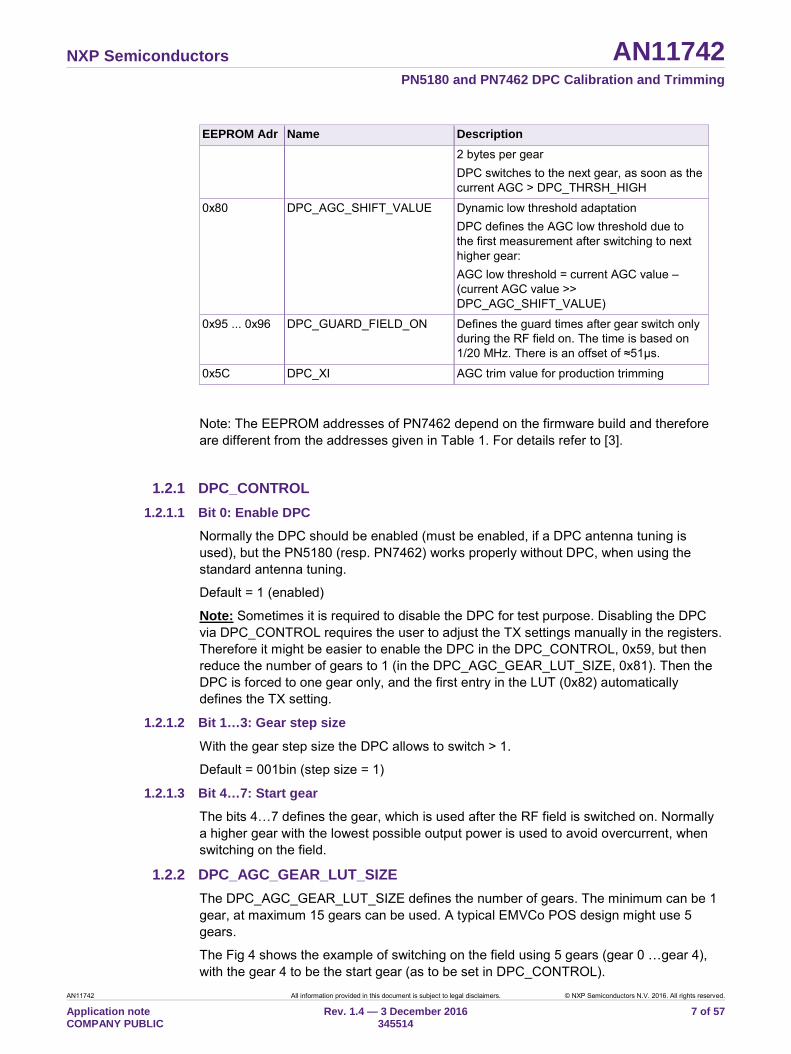
1.2 Parameters of DPC The Table 1 shows the most relevant parameters of the dynamic power control, which must be defined during the calibration process.
Table 1. Relevant parameters of the DPC (PN5180) EEPROM Adr Name Description 0x59 DPC_CONTROL Bit 0 enables the DPC
Bit 1..3 define the gear step size (default = 1) Bit 4…7 define the start gear (= highest gear!)
0x81 DPC_AGC_GEAR_LUT_SIZE This value defines the number of gears. Minimum = 1 = 0x01, maximum = 15 = 0x0F
0c82 … 0x90 DPC_AGC_GEAR_LUT Up to 15 output power settings 1 byte per gear. Definition refer to section 1.2.3.
0x5F … 0x7C DPC_THRSH_HIGH Up to 15 AGC high threshold values
NXP Semiconductors AN11742 PN5180 and PN7462 DPC Calibration and Trimming
AN11742 All information provided in this document is subject to legal disclaimers. © NXP Semiconductors N.V. 2016. All rights reserved.
Application note COMPANY PUBLIC
Rev. 1.4 — 3 December 2016 345514
7 of 57
EEPROM Adr Name Description 2 bytes per gear DPC switches to the next gear, as soon as the current AGC > DPC_THRSH_HIGH
0x80 DPC_AGC_SHIFT_VALUE Dynamic low threshold adaptation DPC defines the AGC low threshold due to the first measurement after switching to next higher gear: AGC low threshold = current AGC value –(current AGC value >> DPC_AGC_SHIFT_VALUE)
0x95 ... 0x96 DPC_GUARD_FIELD_ON Defines the guard times after gear switch only during the RF field on. The time is based on 1/20 MHz. There is an offset of ≈51µs.
0x5C DPC_XI AGC trim value for production trimming
Note: The EEPROM addresses of PN7462 depend on the firmware build and therefore are different from the addresses given in Table 1. For details refer to [3].
1.2.1 DPC_CONTROL 1.2.1.1 Bit 0: Enable DPC
Normally the DPC should be enabled (must be enabled, if a DPC antenna tuning is used), but the PN5180 (resp. PN7462) works properly without DPC, when using the standard antenna tuning.
Default = 1 (enabled)
Note: Sometimes it is required to disable the DPC for test purpose. Disabling the DPC via DPC_CONTROL requires the user to adjust the TX settings manually in the registers. Therefore it might be easier to enable the DPC in the DPC_CONTROL, 0x59, but then reduce the number of gears to 1 (in the DPC_AGC_GEAR_LUT_SIZE, 0x81). Then the DPC is forced to one gear only, and the first entry in the LUT (0x82) automatically defines the TX setting.
1.2.1.2 Bit 1…3: Gear step size
With the gear step size the DPC allows to switch > 1.
Default = 001bin (step size = 1)
1.2.1.3 Bit 4…7: Start gear
The bits 4…7 defines the gear, which is used after the RF field is switched on. Normally a higher gear with the lowest possible output power is used to avoid overcurrent, when switching on the field.
1.2.2 DPC_AGC_GEAR_LUT_SIZE The DPC_AGC_GEAR_LUT_SIZE defines the number of gears. The minimum can be 1 gear, at maximum 15 gears can be used. A typical EMVCo POS design might use 5 gears.
The Fig 4 shows the example of switching on the field using 5 gears (gear 0 …gear 4), with the gear 4 to be the start gear (as to be set in DPC_CONTROL).

NXP Semiconductors AN11742 PN5180 and PN7462 DPC Calibration and Trimming
AN11742 All information provided in this document is subject to legal disclaimers. © NXP Semiconductors N.V. 2016. All rights reserved.
Application note COMPANY PUBLIC
Rev. 1.4 — 3 December 2016 345514
8 of 57
(1) 5 gears (2) DPC_GUARD_FIELD_ON = 0x07D0 = 2000 => 100µs + ≈ 51µs offset
Fig 4. RF Field on with DPC
1.2.3 DPC_AGC_GEAR_LUT (TX Output power settings) Each gear defines a different TX output power setting. The lowest gear uses a setting with the highest output power. The gear x+1 always uses a lower output power than gear x.
For each gear the TX output power setting can and must be defined, using the DPC_AGC_GEAR_LUT. The possible settings are shown in Fig 5 and Table 2.

NXP Semiconductors AN11742 PN5180 and PN7462 DPC Calibration and Trimming
AN11742 All information provided in this document is subject to legal disclaimers. © NXP Semiconductors N.V. 2016. All rights reserved.
Application note COMPANY PUBLIC
Rev. 1.4 — 3 December 2016 345514
9 of 57
(1) Low nibble of DPC_AGC_GEAR_LUT entry
Fig 5. TX Power setting bit 0…3
Table 2. TX Power Settings (bit 7...0) Bit 11 … 8 are not taken into account. Bit Name Description 0 TX_CW_AMP_REF2TVDD 1: TX supply = TVDD – TX_CW_AMPLITUDE_RM
0: TX supply = 3V – TX_CW_AMPLITUDE_RM
2…1 TX_CW_AMPLITUDE_RM 00 = 150mV 01 = 250mV 10 = 500mV 11 = 1V
3 TX_CW_TO_MAX_RM 1: maximum power (TX supply = TVDD) 0: TX supply due to TX_CW_AMP_REF2TVDD & TX_CW_AMPLITUDE_RM
7...4 TX_GSN_CW_RM 0000: lowest power level 1111: highest power level
11 … 8 Don’t care Are not taken into account
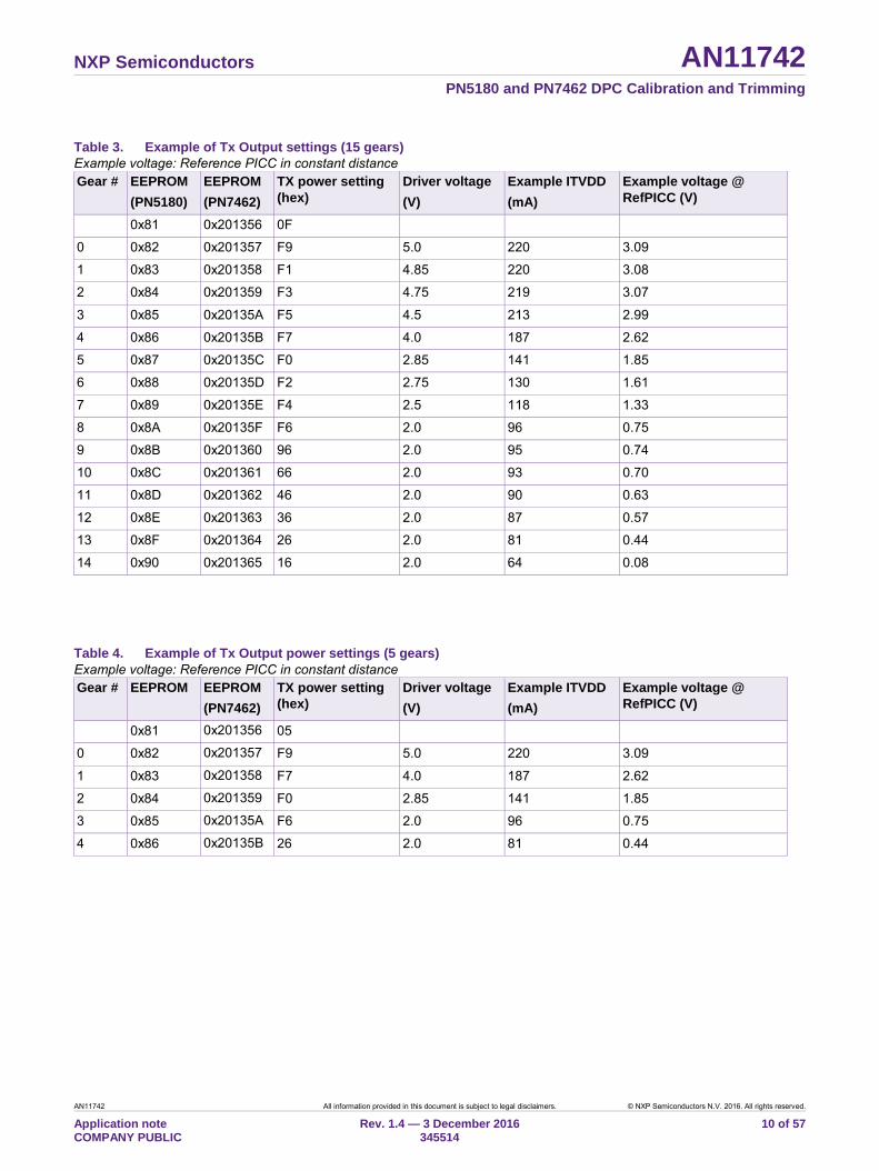
Table 3 shows the example of TX output power settings for 15 gears, Table 4 shows the example for 5 gears. The address 0x81 is shown for reference, indicating the number of valid gears (DPC_AGC_GEAR_LUT_SIZE), as taken into account by the PN5180 (resp. PN7462) DPC.
The column 5 shows the ITVDD value of the example, the column 6 the DC voltage level, measured at the EMVCo Reference PICC, positioned in 4cm above the antenna. The settings for the 5 gears in Table 4 are chosen in a way to achieve similar steps in the ITVDD between each gear.
NXP Semiconductors AN11742 PN5180 and PN7462 DPC Calibration and Trimming
AN11742 All information provided in this document is subject to legal disclaimers. © NXP Semiconductors N.V. 2016. All rights reserved.
Application note COMPANY PUBLIC
Rev. 1.4 — 3 December 2016 345514
10 of 57
Table 3. Example of Tx Output settings (15 gears) Example voltage: Reference PICC in constant distance Gear # EEPROM
(PN5180) EEPROM (PN7462)
TX power setting (hex)
Driver voltage (V)
Example ITVDD (mA)
Example voltage @ RefPICC (V)
0x81 0x201356 0F
0 0x82 0x201357 F9 5.0 220 3.09
1 0x83 0x201358 F1 4.85 220 3.08
2 0x84 0x201359 F3 4.75 219 3.07
3 0x85 0x20135A F5 4.5 213 2.99
4 0x86 0x20135B F7 4.0 187 2.62
5 0x87 0x20135C F0 2.85 141 1.85
6 0x88 0x20135D F2 2.75 130 1.61
7 0x89 0x20135E F4 2.5 118 1.33
8 0x8A 0x20135F F6 2.0 96 0.75
9 0x8B 0x201360 96 2.0 95 0.74
10 0x8C 0x201361 66 2.0 93 0.70
11 0x8D 0x201362 46 2.0 90 0.63
12 0x8E 0x201363 36 2.0 87 0.57
13 0x8F 0x201364 26 2.0 81 0.44
14 0x90 0x201365 16 2.0 64 0.08
Table 4. Example of Tx Output power settings (5 gears) Example voltage: Reference PICC in constant distance Gear # EEPROM EEPROM
(PN7462) TX power setting (hex)
Driver voltage (V)
Example ITVDD (mA)
Example voltage @ RefPICC (V)
0x81 0x201356 05
0 0x82 0x201357 F9 5.0 220 3.09
1 0x83 0x201358 F7 4.0 187 2.62
2 0x84 0x201359 F0 2.85 141 1.85
3 0x85 0x20135A F6 2.0 96 0.75
4 0x86 0x20135B 26 2.0 81 0.44
NXP Semiconductors AN11742 PN5180 and PN7462 DPC Calibration and Trimming
AN11742 All information provided in this document is subject to legal disclaimers. © NXP Semiconductors N.V. 2016. All rights reserved.
Application note COMPANY PUBLIC
Rev. 1.4 — 3 December 2016 345514
11 of 57
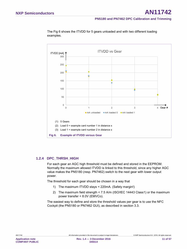
The Fig 6 shows the ITVDD for 5 gears unloaded and with two different loading examples.
(1) 5 Gears (2) Load 0 = example card number 1 in distance x (3) Load 1 = example card number 2 in distance x
Fig 6. Example of ITVDD versus Gear
1.2.4 DPC_THRSH_HIGH For each gear an AGC high threshold must be defined and stored in the EEPROM. Normally the maximum allowed ITVDD is linked to this threshold, since any higher AGC value makes the PN5180 (resp. PN7462) switch to the next gear with lower output power.
The threshold for each gear should be chosen in a way that
1) The maximum ITVDD stays < 220mA. (Safety margin!)
2) The maximum field strength < 7.5 A/m (ISO/IEC 14443 Class1) or the maximum power transfer < 8.0V (EMVCo).
The easiest way to define and store the threshold values per gear is to use the NFC Cockpit (the PN5180 or PN7462 GUI), as described in section 3.3.
NXP Semiconductors AN11742 PN5180 and PN7462 DPC Calibration and Trimming
AN11742 All information provided in this document is subject to legal disclaimers. © NXP Semiconductors N.V. 2016. All rights reserved.
Application note COMPANY PUBLIC
Rev. 1.4 — 3 December 2016 345514
12 of 57
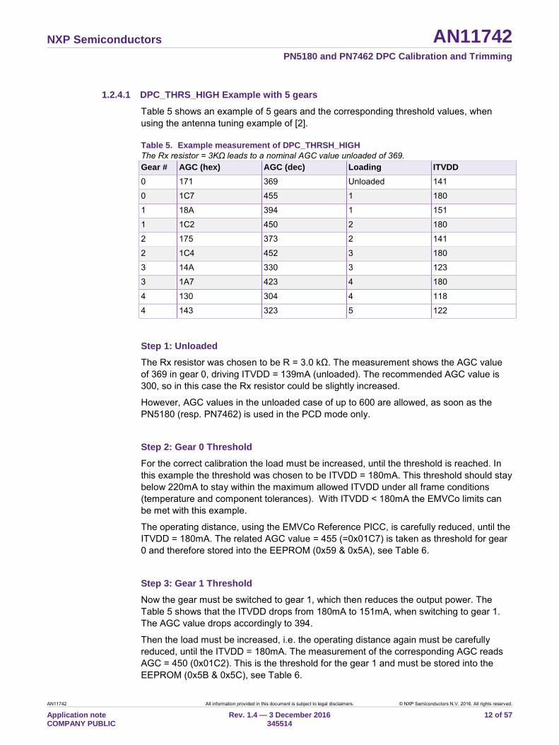
1.2.4.1 DPC_THRS_HIGH Example with 5 gears
Table 5 shows an example of 5 gears and the corresponding threshold values, when using the antenna tuning example of [2].
Table 5. Example measurement of DPC_THRSH_HIGH The Rx resistor = 3KΩ leads to a nominal AGC value unloaded of 369. Gear # AGC (hex) AGC (dec) Loading ITVDD 0 171 369 Unloaded 141
0 1C7 455 1 180
1 18A 394 1 151
1 1C2 450 2 180
2 175 373 2 141
2 1C4 452 3 180
3 14A 330 3 123
3 1A7 423 4 180
4 130 304 4 118
4 143 323 5 122
Step 1: Unloaded
The Rx resistor was chosen to be R = 3.0 kΩ. The measurement shows the AGC value of 369 in gear 0, driving ITVDD = 139mA (unloaded). The recommended AGC value is 300, so in this case the Rx resistor could be slightly increased.
However, AGC values in the unloaded case of up to 600 are allowed, as soon as the PN5180 (resp. PN7462) is used in the PCD mode only.
Step 2: Gear 0 Threshold
For the correct calibration the load must be increased, until the threshold is reached. In this example the threshold was chosen to be ITVDD = 180mA. This threshold should stay below 220mA to stay within the maximum allowed ITVDD under all frame conditions (temperature and component tolerances). With ITVDD < 180mA the EMVCo limits can be met with this example.
The operating distance, using the EMVCo Reference PICC, is carefully reduced, until the ITVDD = 180mA. The related AGC value = 455 (=0x01C7) is taken as threshold for gear 0 and therefore stored into the EEPROM (0x59 & 0x5A), see Table 6.
Step 3: Gear 1 Threshold
Now the gear must be switched to gear 1, which then reduces the output power. The Table 5 shows that the ITVDD drops from 180mA to 151mA, when switching to gear 1. The AGC value drops accordingly to 394.
Then the load must be increased, i.e. the operating distance again must be carefully reduced, until the ITVDD = 180mA. The measurement of the corresponding AGC reads AGC = 450 (0x01C2). This is the threshold for the gear 1 and must be stored into the EEPROM (0x5B & 0x5C), see Table 6.

NXP Semiconductors AN11742 PN5180 and PN7462 DPC Calibration and Trimming
AN11742 All information provided in this document is subject to legal disclaimers. © NXP Semiconductors N.V. 2016. All rights reserved.
Application note COMPANY PUBLIC
Rev. 1.4 — 3 December 2016 345514
13 of 57
Step 4: Gear 2 Threshold
Again the gear must be switched now to the next gear, which then reduces the outpout power. Then the operating distance must be further decreased, until the ITVDD = 180mA. The corresponding AGC value is the threshold value for the gear 2.
Step 5: all other thresholds
These steps are continued gear by gear, until the maximum load (Reference PICC and any load in zero distance), and / or the last gear with the lowest output power is reached.
Out of this the AGC threshold table for all used gears should be completely stored in the EEPROM as shown for the example in Table 6.
Table 6. Example PN5180 EEPROM content for DPC_THRSH_HIGH Due to the measurement results from Table 5. EEPROM Adr Hex Remark Gear # 0x5F C7 Low byte of high threshold 0
0x60 01 High byte of high threshold 0
0x61 C2 Low byte of high threshold 1
0x62 01 High byte of high threshold 1
0x63 C4 Low byte of high threshold 2
0x64 01 High byte of high threshold 2
0x65 A7 Low byte of high threshold 3
0x66 01 High byte of high threshold 3
0x67 43 Low byte of high threshold 4
0x68 01 High byte of high threshold 4
Now the DPC is calibrated and can be used.
1.2.5 DPC_AGC_SHIFT_VALUE The AGC low threshold is automatically calculated by the PN5180 (resp. PN7462) itself to avoid an oscillation. The calculation parameter can be set in the EEPROM, using the DPC_AGC_SHIFT_VALUE. The DPC_AGC_SHIFT_VALUE defines the hysteresis for the gear switch in form of a shift value.
The AGC low threshold is calculated after the gear has switched, i.e. after the output power (and the AGC value) has decreased:
Dynamic AGC low threshold = new AGC – (new AGC >> DPC_AGC_SHIFT_VALUE)
Recommendation: do not change the DPC_AGC_SHIFT_VALUE.
Example:
DPC_AGC_SHIFT_VALUE = 5

NXP Semiconductors AN11742 PN5180 and PN7462 DPC Calibration and Trimming
AN11742 All information provided in this document is subject to legal disclaimers. © NXP Semiconductors N.V. 2016. All rights reserved.
Application note COMPANY PUBLIC
Rev. 1.4 — 3 December 2016 345514
14 of 57
The AGC after switching from gear 0 to gear 1 might be 394(dec). Shifting 5 bits to the right (= dividing through 32) results in 12(dec). So the dynamic AGC low threshold for gear 1 becomes 382(dec) = 0x17E.
The default DPC_AGC_SHIFT_VALUE = 0x05.
The higher the DPC_AGC_SHIFT_VALUE gets, the smaller the hysteresis between AGC value after gear switch and the dynamic AGC low threshold becomes.
A lower DPC_AGC_SHIFT_VALUE increases the hysteresis.
1.2.6 DPC_XI Due to production tolerances the AGC values can vary by +/- 30 AGC steps. Therefor the DPC allows a trim procedure correct this variation. This trim procedure corrects the AGC values based on a correction or trim value: DPC_XI.
This trim value must be derived and then stored in the EEPROM (PN51800: 0x5C: PN7462: 0x201353) for every PN5180 (resp. PN7462) device, i.e. for every reader device during production.
1.2.6.1 Define Reference AGC value
The first and original DPC antenna tuning and the DPC calibration is done with a PN5180 (resp. PN7462) device, using the DPC_XI = 0. This device can be seen like a reference device (“golden device”).
The Reference AGC value must be read, using gear 0 under unloaded condition (read RF_STATUS register, bit 0 …9). This Reference AGC will be used for the Trim procedure later on during production.
1.2.6.2 Trim production device
For each production device, i.e. for all devices other than the “golden device”, the current AGC value must be read, using gear 0 under unloaded condition (read RF_STATUS register, bit 0 …9).
Note: It might be required to “force” the device into gear 0, since the DPC settings, which are based on the Reference AGC might switch gear already under unloaded conditions.
Then the DPC_XI can be calculated:
DPC_XI value = Reference AGC value – current AGC value
Then the DPC_XI must be stored into the EEPROM (0x5C).
Note: The DPC_XI value might be negative using the complement on two.

NXP Semiconductors AN11742 PN5180 and PN7462 DPC Calibration and Trimming
AN11742 All information provided in this document is subject to legal disclaimers. © NXP Semiconductors N.V. 2016. All rights reserved.
Application note COMPANY PUBLIC
Rev. 1.4 — 3 December 2016 345514
15 of 57
2. DPC Correlation test The DPC uses the AGC value to control the output power, i.e. the ITVDD. Therefore it requires a correlation between the ITVDD and the AGC value to allow a proper control mechanism, as shown in Fig 7.
This correlation normally is achieved, if 1. The DPC antenna tuning is applied, i.e. the impedance shows the “symmetrical”
tuning behavior 2. The L0 ≥ Lantenna/2
However, it is strongly recommended to check the correlation for each antenna tuning separately. So one of the first things after antenna tuning is the DPC Correlation test.
AGC value
ITVDD current
Max 250 mA
Linearization curve
Observed AGC value
Predicted current
Fig 7. Correlation between AGC and ITVDD
2.1 Correlation test The correlation test needs to be done with different types of loading to ensure a proper correlation between AGC value and ITVDD for any loading condition.
The easiest way to test this is to define at least two different types of “worst case” loading, e.g. loading with a reference PICC and loading with a smart phone (metal).
These two type of loadings typically show opposite behavior in terms of detuning: typically the EMVCo Reference PICC turns the impedance curve in the smith chart clockwise, while a metal loading like a smart phone typically turns the curve counter clockwise (refer to Fig 1).
For each of these loading conditions the ITVDD versus AGC value should be measured. The result can be shown in a diagram like shown in Fig 8.
Fig 8a shows a good correlation, where the correlation between AGC value and ITVDD is “linear” enough and also close enough between the two different loading conditions. This tuning can be used to calibrate the DPC.

NXP Semiconductors AN11742 PN5180 and PN7462 DPC Calibration and Trimming
AN11742 All information provided in this document is subject to legal disclaimers. © NXP Semiconductors N.V. 2016. All rights reserved.
Application note COMPANY PUBLIC
Rev. 1.4 — 3 December 2016 345514
16 of 57
Fig 8b shows a bad correlation. In this example a too low value of L0 has been chosen. This results in a non-linear behavior. Certain AGC values correspond to multiple ITVDD (= output power levels). With this antenna tuning the DPC will not work.
a. Good correlation example b. Bad correlation example
Fig 8. Correlation example
The correlation test is supported by the NFC Cockpit.
2.2 Correlation test with the NFC Cockpit The easiest way to perform a correlation test is to use the NFC Cockpit.
2.2.1 PN5180 The PN5180 Evaluation board with the tuned antenna must be connected to the PC via USB.
Note: Alternatively the NFC Cockpit VCOM version can be used on the final reader hardware, as soon as VCOM interface is supported by it.
An ITVDD measurement is required to perform the correlation test and the DPC calibration itself, e.g. connecting an Ampere meter at jumper JP3, as shown in Fig 9.

NXP Semiconductors AN11742 PN5180 and PN7462 DPC Calibration and Trimming
AN11742 All information provided in this document is subject to legal disclaimers. © NXP Semiconductors N.V. 2016. All rights reserved.
Application note COMPANY PUBLIC
Rev. 1.4 — 3 December 2016 345514
17 of 57
(1) An external power supply should be used for all analog tests.
Fig 9. Jumper of the PN5180 Evaluation board
Note: All analog tests must be done with a proper power supply, especially for the TVDD. For the PN5180 evaluation board that means either an external power supply with at least 7.5 (AC or DC) is connected to the power plug of the evaluation board, or the TVDD is supplied directly by an external power supply, e.g. using the TVDD pin of the jumper JP3.
Note: In the final hardware the same applies, i.e. the hardware must provide a proper power supply and the ITVDD must be measurable, if the final hardware in combination with the VCOM version of the NFC Cockpit is used for the correlation test.
2.2.2 PN7462 The PN7462 Evaluation board with the tuned antenna must be connected to the PC via USB.
An ITVDD measurement is required to perform the correlation test and the DPC calibration itself, e.g. connecting an external power supply to jumper JP16, as shown in Fig 10.

NXP Semiconductors AN11742 PN5180 and PN7462 DPC Calibration and Trimming
AN11742 All information provided in this document is subject to legal disclaimers. © NXP Semiconductors N.V. 2016. All rights reserved.
Application note COMPANY PUBLIC
Rev. 1.4 — 3 December 2016 345514
18 of 57
(1) An external power supply should be connected for all analog tests.
Fig 10. Jumper of the PN7462 Evaluation board
2.2.3 Step 1: ITVDD unloaded The first step of the correlation test is to measure and enter the ITVDD under no loading. The protocol settings of Type A should be loaded, and then the RF field must be switched on.
Note: It might be good to limit the external ITVDD to avoid damage, in case the antenna tuning is wrong, or some external load detunes the antenna too much and therefore increases the ITVDD too much. This might easily exceed the allowed limit before the DPC is calibrated and enabled.
The measured ITVDD (unloaded) must be entered into the NFC Cockpit as shown in Fig 11, Step 1. This ITVDD value is the starting point of the correlation test.

NXP Semiconductors AN11742 PN5180 and PN7462 DPC Calibration and Trimming
AN11742 All information provided in this document is subject to legal disclaimers. © NXP Semiconductors N.V. 2016. All rights reserved.
Application note COMPANY PUBLIC
Rev. 1.4 — 3 December 2016 345514
19 of 57
Fig 11. Correlation test steps 1…4
2.2.4 Step 2: Step size Then the step size must be defined, as shown in Fig 11, step 2. The correlation test is done in steps of ITVDD, starting with the ITVDD unloaded, using the defined step size. The smaller the step size is, the more steps are tested. Typically a step size of 10mA is a good choice.
2.2.5 Step 3: ITVDD max The next required entry is the maximum limit of the ITVDD, at which the test will be stopped, as shown in Fig 11, step 3.
The default value is the maximum allowed ITVDD of 250mA.
2.2.6 Step 4: Start correlation test Per default two loading cases are tested, but of course more can be chosen. As mentioned in section 2, two loading cases with the opposite detuning behavior normally are sufficient. So typically the loading with a Reference PICC as well as with a large smart phone (= piece of metal) should be tested.
When the correlation is started, an entry field appears as shown in Fig 11, which asks for a name of the first loading case. A meaningful name can be entered, e.g. “Reference PICC” or “Metal”. This name is used to indicate the test results related to this loading case in the later result table.

NXP Semiconductors AN11742 PN5180 and PN7462 DPC Calibration and Trimming
AN11742 All information provided in this document is subject to legal disclaimers. © NXP Semiconductors N.V. 2016. All rights reserved.
Application note COMPANY PUBLIC
Rev. 1.4 — 3 December 2016 345514
20 of 57
2.2.7 Step 5: ITVDD / AGC measurement loading case 1 The starting point of the correlation test is the minimum ITVDD under unloaded condition. The previously entered ITVDD unloaded appears as well as the corresponding AGC value as shown in Fig 12.
Note: The example as shown in Fig 16 uses an example antenna tuning with ITVDD = 77mA unloaded.
For the first step the loading condition (unloaded) must be valid to achieve the given ITVDD, and then the value must be stored by pressing the <Store AGC Value>. Another info window appears, indicating the pair of ITVDD and corresponding AGC value, which then will be stored.
When stored, the first line of the measurement table will be shown, indicating the ITVDD and the AGC value in hexadecimal and decimal.
(1) The Version of the NFC Cockpit still has a bug to reduce the ITVDD, when starting the correlation test.
Fig 12. Correlation test step 5
The ITVDD given by the NFC Cockpit is then automatically increased by the step size (e.g.10mA).
Now the load on the antenna must be changed: the operating distance of the Reference PICC (or metal or whatever the first loading case is) must be changed in such a way that

NXP Semiconductors AN11742 PN5180 and PN7462 DPC Calibration and Trimming
AN11742 All information provided in this document is subject to legal disclaimers. © NXP Semiconductors N.V. 2016. All rights reserved.
Application note COMPANY PUBLIC
Rev. 1.4 — 3 December 2016 345514
21 of 57
the ITVDD measurement (using the Ampere meter) shows the same ITVDD value as the NFC Cockpit.
As soon as the Ampere meter shows the given (required) ITVDD, the AGC Value must be stored (<Store AGC Value>). Then the NFC Cockpit again increases the given (required) ITVDD by one step.
This measurement then must be continued step by step: the load must be adapted always to meet the given (required) ITVDD, and then the corresponding AGC Value must be stored (<Store AGC Value>).
2.2.8 Step 6: ITVDD / AGC measurement loading case 2 When the maximum ITVDD is reached the NFC Cockpit automatically starts the second part of the correlation test, using the “opposite” loading, e.g. metal, as shown in Fig 13.
This second part then must be executed in the same way like the first part (step 5), except that the different load is used.
(1) The AGC values do not exceed 328(dec) since the loading cannot be increased any further than ITVDD = 190mA, when using the Reference PICC as load.
Fig 13. Correlation test start of second loading case

NXP Semiconductors AN11742 PN5180 and PN7462 DPC Calibration and Trimming
AN11742 All information provided in this document is subject to legal disclaimers. © NXP Semiconductors N.V. 2016. All rights reserved.
Application note COMPANY PUBLIC
Rev. 1.4 — 3 December 2016 345514
22 of 57
2.2.9 Step 7: Store the result As soon as the last measurement is done, the NFC Cockpit allows the export of the table, as shown in Fig 14.
a. Export of the measurement table b. Measurement table in Excel
Fig 14. Correlation test last step
This table then can be opened e.g. with Microsoft Excel to easily draw a graph as shown in Fig 15.
Note: In the shown result the AGC value does not exceed 328 for the loading case 1 (“Reference PICC”). In that case the load (=Reference PICC) was already in zero distance laying on the PCD antenna, so no further increase of ITVDD (and AGC) was possible.

NXP Semiconductors AN11742 PN5180 and PN7462 DPC Calibration and Trimming
AN11742 All information provided in this document is subject to legal disclaimers. © NXP Semiconductors N.V. 2016. All rights reserved.
Application note COMPANY PUBLIC
Rev. 1.4 — 3 December 2016 345514
23 of 57
(1) The AGC values do not exceed 328(dec) since the loading cannot be increased any further than ITVDD = 190mA, when using the Reference PICC as load.
Fig 15. Correlation test result
3. DPC calibration The DPC calibration must be done to operate a DPC antenna. This calibration defines the AGC threshold values, which make the PN5180 (resp. PN7462) change to the next gear, i.e. which make the PN5180 (resp. PN7462) decrease the output power.
3.1 Prerequisites The DPC calibration requires a DPC antenna tuning (refer to [2]), which meets the correlation requirement as indicated above.
It makes sense to test the Tx wave shapes at least in the “unloaded” case, i.e. in the position with the lowest possible coupling between the PCD antenna and the Reference PICC. In case of EMVCo this is the position in 4cm above the antenna. All other positions should be checked and adjusted later, when the DPC is working.
The Rx coupling resistors must be adjusted to achieve an AGC value of at least 300 unloaded.
Note: The optimum unloaded AGC value for a pure PCD functionality (only NFC Reader mode) is ≈ 600. As soon as the device shall support all NFC modes, the unloaded AGC value should be ≈ 300.
3.2 DPC Calibration minimum requirements This calibration requires the definition of at least 1. Number of gears (DPC_AGC_GEAR_LUT_SIZE)
Details refer to section 1.2.2. 2. Tx Settings per gear (DPC_AGC_GEAR_LUT)
Details refer to section 1.2.3.

NXP Semiconductors AN11742 PN5180 and PN7462 DPC Calibration and Trimming
AN11742 All information provided in this document is subject to legal disclaimers. © NXP Semiconductors N.V. 2016. All rights reserved.
Application note COMPANY PUBLIC
Rev. 1.4 — 3 December 2016 345514
24 of 57
3. Dynamic AGC low threshold (DPC_AGC_SHIFT_VALUE) Details refer to section 1.2.5.
4. AGC high threshold per gear (DPC_THRSH_HIGH) Details refer to 1.2.4.
An easy way to calibrate the DPC is provided by the NFC Cockpit.
3.3 Calibration procedure with the NFC Cockpit The DPC calibration is started with the NFC Cockpit as shown in Fig 16. The EEPROM LUT might be cleared (overwritten with 00), just to get clean table.
Note: The PN5180 NFC Cockpit allows to store the complete PN5180 EEPROM content into an XML file, and later reload this XML file back into the PN5180. It might be a good idea to save the EEPROM content as backup before changing the EEPROM.
Note: The PN7462 NFC Cockpit allows a storage of the DPC EEPROM settings into an XML or Binary file. The XML might be used for documentation purpose, while the binary can be directly loaded into the PN7462, using the NFC Cockpit or PN7462 “USB mass storage” mode. It might be good to save EEPROM content as backup before changing the EEPROM.
The number of gears must be entered as shown in Fig 16. This automatically generates the table below with the given number of entries (one per gear).
(1) The gear table starts with gear 0 in the first row (up to gear 4), even though the NFC Cockpit shows a number 1 (up to 5).
Fig 16. DPC Calibration Step 1
In the nest step the maximum allowed ITVDD must be entered as shown in Fig 17.

NXP Semiconductors AN11742 PN5180 and PN7462 DPC Calibration and Trimming
AN11742 All information provided in this document is subject to legal disclaimers. © NXP Semiconductors N.V. 2016. All rights reserved.
Application note COMPANY PUBLIC
Rev. 1.4 — 3 December 2016 345514
25 of 57
(1) ITVDD max = 180mA gives a lot of margin.
Fig 17. DPC Calibration Step 2
Then the Tx settings per gear must be entered, as shown in Fig 18. The settings can be chosen as described in section 1.2.3.
(1) In this example 5 gears have been chosen.
Fig 18. DPC Calibration Step 3
Then the calibration itself can be started. The ITVDD must be measured like in section 3. In the first step the NFC Cockpit starts with the gear 0, i.e. with maximum output power. The load must be adapted, until the ITVDD reaches the chosen ITVDD limit. Normally
NXP Semiconductors AN11742 PN5180 and PN7462 DPC Calibration and Trimming
AN11742 All information provided in this document is subject to legal disclaimers. © NXP Semiconductors N.V. 2016. All rights reserved.
Application note COMPANY PUBLIC
Rev. 1.4 — 3 December 2016 345514
26 of 57
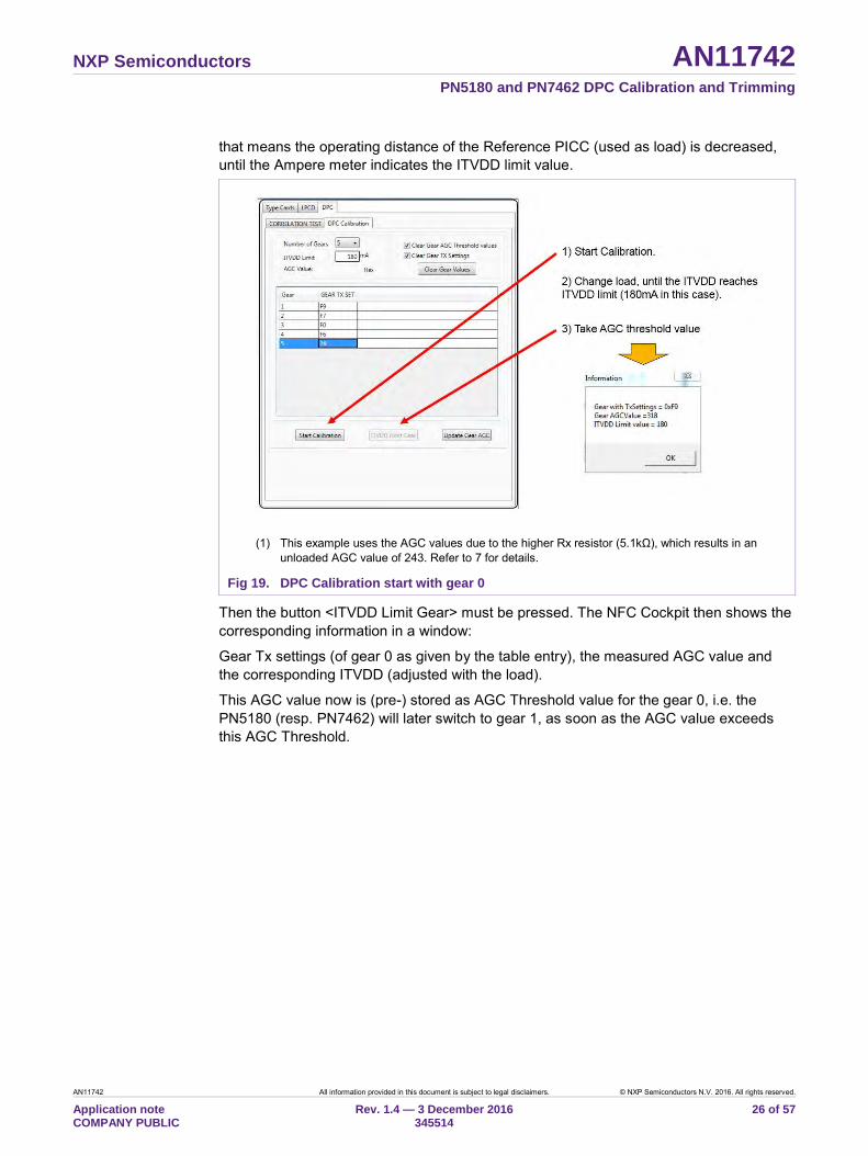
that means the operating distance of the Reference PICC (used as load) is decreased, until the Ampere meter indicates the ITVDD limit value.
(1) This example uses the AGC values due to the higher Rx resistor (5.1kΩ), which results in an unloaded AGC value of 243. Refer to 7 for details.
Fig 19. DPC Calibration start with gear 0
Then the button <ITVDD Limit Gear> must be pressed. The NFC Cockpit then shows the corresponding information in a window:
Gear Tx settings (of gear 0 as given by the table entry), the measured AGC value and the corresponding ITVDD (adjusted with the load).
This AGC value now is (pre-) stored as AGC Threshold value for the gear 0, i.e. the PN5180 (resp. PN7462) will later switch to gear 1, as soon as the AGC value exceeds this AGC Threshold.

NXP Semiconductors AN11742 PN5180 and PN7462 DPC Calibration and Trimming
AN11742 All information provided in this document is subject to legal disclaimers. © NXP Semiconductors N.V. 2016. All rights reserved.
Application note COMPANY PUBLIC
Rev. 1.4 — 3 December 2016 345514
27 of 57
Fig 20. DPC Calibration finish gear 0
Then the NFC Cockpit automatically switches to the next gear (gear 1), which reduces the ITVDD (and the AGC value).
Again the load must be adapted now, until the ITVDD Limit is reached, i.e. the operating distance of the load must be decreased. When the Ampere meter indicates the ITVDD limit, again the button <ITVDD Limit Gear> must be pressed.
Fig 21. DPC calibration with gear 1
Now the NFC Cockpit shows the Gear Tx settings (of gear 1 as given by the table entry), the measured AGC value and the corresponding ITVDD (adjusted with the load).

NXP Semiconductors AN11742 PN5180 and PN7462 DPC Calibration and Trimming
AN11742 All information provided in this document is subject to legal disclaimers. © NXP Semiconductors N.V. 2016. All rights reserved.
Application note COMPANY PUBLIC
Rev. 1.4 — 3 December 2016 345514
28 of 57
This process must be continued gear by gear: 1. The NFC Cockpit switches to the next gear. 2. The load must be adapted until the ITVDD (Ampere meter) reaches the ITVDD limit. 3. The <ITVDD Limit Gear> (pre-) stores the AGC Threshold value for the
corresponding gear.
When the calibration is done, the AGC Threshold values are (pre-) stored in a table as shown in Fig 22.
Pressing the <Update Gear AGC> stores the whole table into the EEPROM. Now the DPC calibration is done.
(1) <Update Gear AGC> stores the DPC_AGC_GEAR_LUT_SIZE, the related DPC_AGC_GEAR_LUT, and all the measured DPC_THRSH_HIGH.
Fig 22. DPC calibration storing the DPC settings

NXP Semiconductors AN11742 PN5180 and PN7462 DPC Calibration and Trimming
AN11742 All information provided in this document is subject to legal disclaimers. © NXP Semiconductors N.V. 2016. All rights reserved.
Application note COMPANY PUBLIC
Rev. 1.4 — 3 December 2016 345514
29 of 57
4. Tx Shaping The influence of the EMC filter circuit as well as the TX output itself on the overall antenna behavior is quite strong with the DPC antenna tuning. This allows to use a higher Q factor in the antenna circuit itself, but requires a careful EMC filter design and a Tx Shaping control.
The EMC filter must use inductors with a high Q to achieve a fast fall and rise of the envelope. The higher the Q factor of the EMC filter is, the shorter becomes the fall and rise time of the envelope.
Due to this short fall and rise time in a typical DPC antenna design there are overshoots on both the falling and the rising edge of the envelope as shown in Fig 23. This can be corrected with the TX Shaping features of the PN5180 (resp. PN7462), as described in the following section.
c. Type A pulse, no shaping d. Type A envelope, no shaping
Fig 23. PN5180 Type A pulse, no shaping
4.1 Tx Shaping principle Instead of switching on and off the carrier (@ 100%AM) or switching between two different carrier levels (e.g. @ 10%AM), the PN5180 (resp. PN7462) allows to control the change from unmodulated carrier to modulated carrier and again from modulated carrier to unmodulated carrier.
So basically a standard pulse, like a type A pulse as shown in Fig 24a, is extended from 2 to 4 states:

NXP Semiconductors AN11742 PN5180 and PN7462 DPC Calibration and Trimming
AN11742 All information provided in this document is subject to legal disclaimers. © NXP Semiconductors N.V. 2016. All rights reserved.
Application note COMPANY PUBLIC
Rev. 1.4 — 3 December 2016 345514
30 of 57
1. Unmodulated carrier (= CW) 2. Undershoot pattern (= falling edge) 3. Modulated carrier (e.g. carrier off or 10% settings) 4. SC Shaping (= rising edge)
These four states are shown in an example in Fig 24b. Within the two “transition” states several parameters can be set to define the falling edge and rising edge behavior.
In principle the transition state length can be defined (see Fig 24b), the rise and fall time (Fig 25a) and the residual carrier in case of the 100% AM (Fig 25b).
a. No Tx Shaping b. Tx Shaping: Undershoot pattern & SC Shaping
Fig 24. Tx Shaping principle 1
a. Tx Shaping: Rise and Fall time b. TX Shaping: Residual carrier
Fig 25. Tx Shaping principle 2
Three parameters can even by dynamically adapted based on the DPC using the AWC:
• Fall time
• Rise time

NXP Semiconductors AN11742 PN5180 and PN7462 DPC Calibration and Trimming
AN11742 All information provided in this document is subject to legal disclaimers. © NXP Semiconductors N.V. 2016. All rights reserved.
Application note COMPANY PUBLIC
Rev. 1.4 — 3 December 2016 345514
31 of 57
• Residual carrier
Note: The residual carrier sets the modulation index as such, if no 100% AM is enabled (e.g. for ISO/IEC 14443 type B). In case of 100% AM it only sets the residual carrier for the transition phase.
4.2 Wave shape test set up The wave shape tests require a Reference PICC to load the PN5180 (resp. PN7462) antenna properly while testing the wave shapes. The wave shape test signal is derived from the Reference PICC, as defined in ISO/IEC 10373-6 or EMVCo Book D or NFC Forum Specifications.
For the optimization of the shaping it might be helpful to connect a probe of the oscilloscope to one of the TX output pins of the PN5180 (resp. PN7462). The principle of the whole setup is shown in Fig 26.
(1) Reference PICC defined by ISO/IEC 10373-6, EMVCo Book D or NFC Forum specification
Fig 26. TX shaping test setup
Note: This probe connected to TX1 or TX2 slightly disturbs the wave shape itself, so the final compliance test must be done without this probe connection.
The wave shape test should be started with the maximum possible operating distance, i.e. with the minimum loading effect. For EMVCo this is at 4cm distance, for any ISO/IEC 14443 test it is at the minimum field strength limit (e.g. at 1.5A/m for Class1).
This automatically results in a gear 0 setting, i.e. the PN5180 (resp. PN7462) drives the maximum output power. The typical envelope looks like shown in Fig 23, as long as neither the undershoot / overshoot protection nor the TX Shaping is enabled.
Note: The measurement of the TX output is done with a digital low pass filter with a cut off frequency of 30MHz. This reduces the noise level and removes any possible spikes on the tested signal.

NXP Semiconductors AN11742 PN5180 and PN7462 DPC Calibration and Trimming
AN11742 All information provided in this document is subject to legal disclaimers. © NXP Semiconductors N.V. 2016. All rights reserved.
Application note COMPANY PUBLIC
Rev. 1.4 — 3 December 2016 345514
32 of 57
4.3 Differences PN5180 versus PN7462 The DPC as well the TX Shaping functionality is the same on PN5180 and on PN7462. Still some small details related to the memory structure are different. The PN5180 offers “virtual registers”, which allow a very consistent handling.
The PN7462 needs to deal with the original CLIF registers.
Therefore in both cases the same functionality can be found in slightly different registers.
4.3.1 PN5180 relevant registers The PN5180 provides four Tx Shaping related registers, of which three registers are relevant:
TX_UNDERSHOOT_CONFIG (0x0014)
• TX_UNDERSHOOT_PATTERN: don‘t touch
• TX_UNDERSHOOT_PATTERN_LEN: important
• TX_UNDERSHOOT_PROT_ENABLE: should be 1
TX_OVERSHOOT_CONFIG (0x0015)
• TX_OVERSHOOT_PATTERN: don‘t touch
• TX_OVERSHOOT_PATTERN_LEN: not important!
• TX_OVERSHOOT_PROT_ENABLE: should be 0!
RF_CONTROL_TX (0x0020)
• TX_RESIDUAL_CARRIER_OV_PREV: not important, if TX_OVERSHOOT_PROT_ENABLE = 0
• TX_RESIDUAL_CARRIER: a low residual carrier might be good
• TX_SET_BYPASS_SC_SHAPING: should be 0 to allow SC Shaping
• TX_SET_SLEW_SHUNTREG: don‘t touch
• TX_SET_TAU_MOD_FALLING: important!
• TX_SET_TAU_MOD_RISING: important!
RF_CONTROL_TX_CLK (0x0021)
• TX_CLK_MODE_OVUN_PREV: Type A: use 101 instead 111 to slow down the falling edge
• TX_CLK_MODE_RM: for type A it is typically 001, for type B it must be 111
4.3.2 PN7462 relevant registers The PN7562 provides four Tx Shaping related registers, of which three registers are relevant:
CLIF_TX_UNDERSHOOT_CONFIG_REG (address 0058h)
• TX_UNDERSHOOT_PATTERN: don‘t touch
• TX_UNDERSHOOT_PATTERN_LEN: important
• TX_UNDERSHOOT_PROT_ENABLE: should be 1
CLIF_TX_OVERSHOOT_CONFIG_REG register (address 0054h)

NXP Semiconductors AN11742 PN5180 and PN7462 DPC Calibration and Trimming
AN11742 All information provided in this document is subject to legal disclaimers. © NXP Semiconductors N.V. 2016. All rights reserved.
Application note COMPANY PUBLIC
Rev. 1.4 — 3 December 2016 345514
33 of 57
• TX_OVERSHOOT_PATTERN: don‘t touch
• TX_OVERSHOOT_PATTERN_LEN: not important!
• TX_OVERSHOOT_PROT_ENABLE: should be 0!
CLIF_ANA_TX_SHAPE_CONTROL_REG (address 0128h)
• TX_RESIDUAL_CARRIER_OV_PREV: not important, if TX_OVERSHOOT_PROT_ENABLE = 0
• TX_SET_BYPASS_SC_SHAPING: should be 0 to allow SC Shaping
• TX_SET_SLEW_SHUNTREG: don‘t touch
• TX_SET_TAU_MOD_FALLING: important!
• TX_SET_TAU_MOD_RISING: important!
CLIF_ANA_TX_AMPLITUDE_REG (address 0108h)
• TX_RESIDUAL_CARRIER: low residual carrier might be good
CLIF_ANA_TX_CLK_CONTROL_REG (address 0104h)
• TX_CLK_MODE_OVUN_PREV: Type A: use 101 instead 111 to slow down the falling edge
• TX_CLK_MODE_RM: for type A it is typically 001, for type B it must be 111
4.4 PN5180 and PN7462 relevant settings So independent from the bit position the relevant bit fields for the Tx Shaping are the following 8 settings.
4.4.1.1 TX_UNDERSHOOT_PROT_ENABLE
This bit enables the UNDERSHOOT_PATTERN, applying the TX_UNDERSHOOT_PATTERN_LEN. So it should be enabled to allow the shaping features for the falling edge.
See Fig 27 for example.
4.4.1.2 TX_UNDERSHOOT_PATTERN_LEN
Defines length of the undershoot prevention pattern (value +1). This is one of the key parameters to adjust (reduce) the undershoot, especially for the type A modulation.
See Fig 27 for example.

NXP Semiconductors AN11742 PN5180 and PN7462 DPC Calibration and Trimming
AN11742 All information provided in this document is subject to legal disclaimers. © NXP Semiconductors N.V. 2016. All rights reserved.
Application note COMPANY PUBLIC
Rev. 1.4 — 3 December 2016 345514
34 of 57
a. Pattern length = 0000bin b. Pattern length = 0111bin c. Pattern length = 1111bin
Fig 27. TX undershoot patter length
4.4.2 TX_UNDERSHOOT_PATTERN The undershoot pattern coding can be changed, but other patterns than the default (all 0) are typically not useful. Refer to Fig 26.
a. Default = 0 b. Pattern = 0x0040 c. Pattern = 0x007F
Fig 28. TX Undershoot pattern
4.4.2.1 TX_RESIDUAL_CARRIER
These 7 bit defines the modulation index via the residual carrier:
0 => m = 100%
0x1F => m = 0%
This value is especially relevant for type B modulation.

NXP Semiconductors AN11742 PN5180 and PN7462 DPC Calibration and Trimming
AN11742 All information provided in this document is subject to legal disclaimers. © NXP Semiconductors N.V. 2016. All rights reserved.
Application note COMPANY PUBLIC
Rev. 1.4 — 3 December 2016 345514
35 of 57
a. Residual carrier = 11111bin b. Residual carrier = 11001bin c. Residual carrier = 01111bin
Fig 29. TX undershoot residual carrier
The Fig 30 shows the effect of the TX Residual carrier level, if the TX_CLK_MODE_OVUN_PREV = 101bin (i.e. the residual carrier only applies on the rising edge).
a. Residual carrier = 11111bin b. Residual carrier = 11011bin c. Residual carrier = 10011bin
Fig 30. TX Overshoot Residual carrier
4.4.2.2 TX_SET_BYPASS_SC_SHAPING
Enabling this bit bypasses the “Switched Capacitor” Tx shaping, i.e. disables the shaping control for the rising edge. So this bit must be 0, if the TAU_MOD_RISING settings shall apply.
The rising edge provides the fastest rise time, if TX_SET_BYPASS_SC_SHAPING = 1 (TAU_MOD_RISING does not matter).
4.4.2.3 TX_SET_TAU_MOD_FALLING
This value defines the time constant for the falling edge.
0 => fastest fall time, typically causing a large undershoot
0xF => slowest fall time, typically causing a small undershoot
This parameter is typically used to balance the undershoot requirement with the fall time requirement, and can be dynamically adapted per gear with the AWC.

NXP Semiconductors AN11742 PN5180 and PN7462 DPC Calibration and Trimming
AN11742 All information provided in this document is subject to legal disclaimers. © NXP Semiconductors N.V. 2016. All rights reserved.
Application note COMPANY PUBLIC
Rev. 1.4 — 3 December 2016 345514
36 of 57
a. Tau Mod Falling = 0000bin b. Tau Mod Falling = 1000bin c. Tau Mod Falling = 1111bin
Fig 31. TX undershoot Fall time behavior
4.4.2.4 TX_SET_TAU_MOD_RISING
This value defines the time constant for the rising edge.
0 => fastest rise time, typically causing a large overshoot
0xF => slowest rise time, typically causing a small overshoot
This parameter is typically used to balance the overshoot requirement with the rise time requirement, and can be dynamically adapted per gear with the AWC.
See Fig 32 for example.
a. Tau Mod Rising = 0000bin b. Tau Mod Rising = 0100bin c. Tau Mod Rising = 1111bin
Fig 32. TX overshoot Rise time behavior
4.4.2.5 TX_CLK_MODE_OVUN_PREV
The TX_CLK_MODE_OVUN_PREV defines the TX Clock mode setting for the pattern in the transition states. There are two most useful settings:
• The default setting = 111bin drives the pattern using the push/pull output like during the unmodulated carrier (or like during the modulation for type B)
NXP Semiconductors AN11742 PN5180 and PN7462 DPC Calibration and Trimming
AN11742 All information provided in this document is subject to legal disclaimers. © NXP Semiconductors N.V. 2016. All rights reserved.
Application note COMPANY PUBLIC
Rev. 1.4 — 3 December 2016 345514
37 of 57
• The setting = 101bin only drives the low side of the push/pull output stage (“open drain”), which disables the residual carrier settings, but slows down the carrier during the pattern length.
Note: The TX_CLK_MODE_OVUN_PREV = 101bin typically provides the smoothest falling edge for a type A pulse, but does not allow any dynamic adaptation in the AWC, since the TX_SET_TAU_MOD_FALLING does not apply in this case.
4.5 Remove undershoot Normally the first step in the Tx Shaping adjustment is the reduction of the undershoot in the falling edge of the pulse. Especially for the 100% pulse of type A this undershoot might cause a violation of the ISO or EMVCo shaping requirements.
The undershoot protection must be enabled with TX_UNDERSHOOT_PROT_ENABLE (bit 0).
The undershoot protection pattern and behavior can be defined with:
• Pattern length: the pattern length changes the length of the undershoot pattern from 0000bin to 1111bin (0x0 to 0xF), refer to Fig 27. Typically a pattern length around 3 to 5 turned out to be useful.
• Pattern coding: the default pattern is 0. Other patterns are typically not useful, but can be set, refer to Fig 28.
• TX Clock mode: The TX_CLK_MODE_OVUN_PREV defines the TX Clock mode setting for the pattern. There are two most useful settings:
o The default setting = 111bin drives the pattern using the push/pull output like during the unmodulated carrier (or like during the modulation for type B)
o The setting = 101bin only drives the low side of the push/pull output stage (“open drain”), which disables the residual carrier settings, but slows down the carrier during the pattern length.
• Residual carrier: the TX_RESIDUAL_CARRIER defines the carrier level at the end of the undershoot pattern, if the TX Clock mode is set to 111bin.
This carrier level applies also at the end of the pulse, when the pulse rising edge starts: Therefor the residual carrier setting influences the overshoot (TX Shaping) behavior, too (refer to section 4.4.2.1).
The TX_RESIDUAL_CARRIER is used to set the residual carrier for Type B, too.
Fig 29 shows three different settings:
o The minimum residual carrier with 0x1F (Fig 29a)
o A residual carrier with 0x19 (Fig 29b)
o A residual carrier with 0x0F (Fig 29c)
• Fall time behavior: The TAU_MOD_FALLING defines the fall time behavior, if the TX Clock mode is set to 111bin and the SC Shaping is enabled. The Fig 31 shows three different fall times from minimum (0x0) to maximum (0xF).

NXP Semiconductors AN11742 PN5180 and PN7462 DPC Calibration and Trimming
AN11742 All information provided in this document is subject to legal disclaimers. © NXP Semiconductors N.V. 2016. All rights reserved.
Application note COMPANY PUBLIC
Rev. 1.4 — 3 December 2016 345514
38 of 57
Note: The TX_RESIDUAL_CARRIER_OV_PREV applies only during the overshoot prevention and is typically not used at all.
Note: For a type A pulse the TX Clock mode setting = 101bin allows to use a “low residual carrier” to reduce the undershoot at the beginning of the pulse, independent from the residual carrier settings. The residual carrier level then does only influence the overshoot behavior, and can be adjusted more flexibly.
4.6 Remove overshoot The use of TX overshoot protection is not recommended. The bit 0 (TX_OVERSHOOT_PROT_ENABLE) should be set to 0.
With the TX Shaping the overshoot at the end of the pulse can be reduced. The TX SC Shaping can be enabled with the bit TX_BYPASS_SC_SHAPING, which must be set to 0 (= disable the bypass!).
The overshoot protection pattern and behavior can be defined with:
• Rise time behavior: the TAU_MOD_RISING can be used to increase the rise time, which then decreases the overshoot. The Fig 32 shows three different settings from minimum (0x0) to maximum (0xF).
• Residual carrier: the TX_RESIDUAL_CARRIER defines the carrier level at the end of the pulse, when the rise time of the pulse starts. This is independent from the TX Clock mode setting.
This carrier level applies to the beginning of the pulse, too, if the TX Clock Mode = 111bin: therefore the residual carrier setting influences the undershoot behavior, too (refer to section 4.5).
The TX_RESIDUAL_CARRIER is used to set the residual carrier for Type B, too.
Fig 30 shows three different settings:
o The minimum residual carrier with 0x1F (Fig 30a)
o A residual carrier with 0x1B (Fig 30b)
o A residual carrier with 0x03 (Fig 30c)

NXP Semiconductors AN11742 PN5180 and PN7462 DPC Calibration and Trimming
AN11742 All information provided in this document is subject to legal disclaimers. © NXP Semiconductors N.V. 2016. All rights reserved.
Application note COMPANY PUBLIC
Rev. 1.4 — 3 December 2016 345514
39 of 57
4.7 Examples The TX Shaping examples are shown for a 2 turn antenna as indicated in Fig 33.
a. 68mm x 49mm 2 turn Antenna b. Antenna tuning
Fig 33. Example antenna
4.7.1 Example of a TX shaping setting for type A The Fig 34 shows the standard type A pulse of the example antenna without any TX Shaping. Basically the envelope test of EMVCo fails due to the overshoots.
a. Screenshot from the Oscilloscope b. Screenshot from CETECOM WaveChecker
Fig 34. EMVCo Type A without TX Shaping (fail)
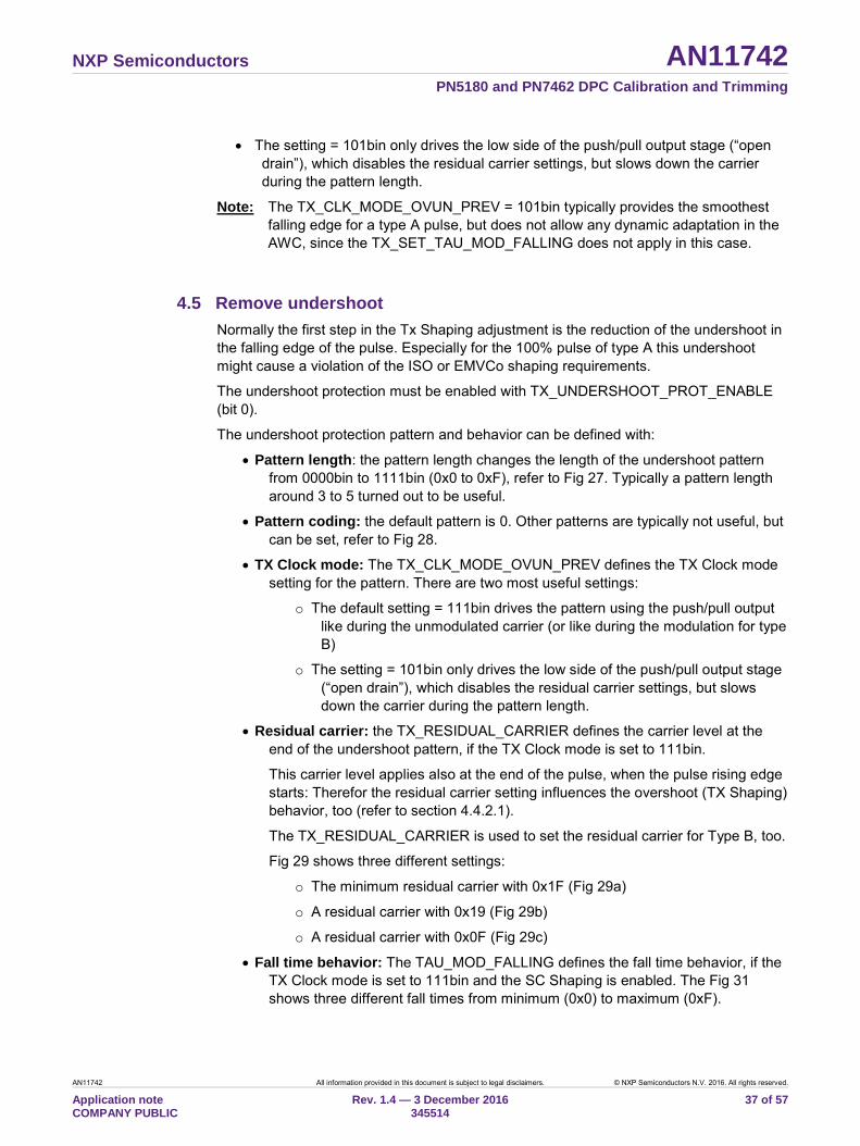
The Fig 35 shows the same antenna, but with enabled TX Shaping, using undershoot protection and TX SC Shaping with the following register settings:
NXP Semiconductors AN11742 PN5180 and PN7462 DPC Calibration and Trimming
AN11742 All information provided in this document is subject to legal disclaimers. © NXP Semiconductors N.V. 2016. All rights reserved.
Application note COMPANY PUBLIC
Rev. 1.4 — 3 December 2016 345514
40 of 57
Table 7. EMVCo Type A with TX Shaping Setting Value
(bin) Comment
TX_UNDERSHOOT_PATTERN_LEN
1111
TX_UNDERSHOOT_PROT_ENABLE 1 Undershoot protection enabled
TX_RESIDUAL_CARRIER 11110
TX_SET_BYPASS_SC_SHAPING 0 SC Shaping enabled
TX_SET_TAU_MOD_FALLING 0100
TX_SET_TAU_MOD_RISING 0011
TX_CLK_MODE_OVUN_PREV 101 Only low side of the push/pull output stage
TX_CLK_MODE_RM 001 Due to type A 100% AM
a. Screenshot from the Oscilloscope b. Screenshot from CETECOM WaveChecker
Fig 35. EMVCo Type A with TX Shaping (pass)
These register settings must then be stored in the EEPROM in the corresponding Protocol area. The NFC Cockpit supports writing the register into the correct position by selecting the protocol, e.g. “TX IOS14443A 106” indicating the area of the transmitter settings for ISO/IEC 14443 type A protocol at 106 kbit/s.

NXP Semiconductors AN11742 PN5180 and PN7462 DPC Calibration and Trimming
AN11742 All information provided in this document is subject to legal disclaimers. © NXP Semiconductors N.V. 2016. All rights reserved.
Application note COMPANY PUBLIC
Rev. 1.4 — 3 December 2016 345514
41 of 57
4.7.2 Example of a TX shaping setting for type B The Fig 36 shows the standard type A pulse of the example antenna without any TX Shaping. Basically the envelope test of EMVCo fails due to the overshoots.
a. Screenshot from the Oscilloscope b. Screenshot from CETECOM WaveChecker
Fig 36. EMVCo Type B without TX Shaping (fail)
The Fig 37 shows the same antenna, but with enabled TX Shaping, using TX SC Shaping with the following register settings:
Table 8. EMVCo Type B with TX Shaping Setting Value
(bin) Comment
TX_UNDERSHOOT_PATTERN_LEN
0000
TX_UNDERSHOOT_PROT_ENABLE 0 Undershoot protection disabled
TX_RESIDUAL_CARRIER 11110
TX_SET_BYPASS_SC_SHAPING 0 SC Shaping enabled
TX_SET_TAU_MOD_FALLING 0001
TX_SET_TAU_MOD_RISING 0110 To slow down the rising edge
TX_CLK_MODE_OVUN_PREV 000 Does not matter, since undershoot protection is disabled.
TX_CLK_MODE_RM 111 Due to type B 10% AM
NXP Semiconductors AN11742 PN5180 and PN7462 DPC Calibration and Trimming
AN11742 All information provided in this document is subject to legal disclaimers. © NXP Semiconductors N.V. 2016. All rights reserved.
Application note COMPANY PUBLIC
Rev. 1.4 — 3 December 2016 345514
42 of 57
a. Screenshot from the Oscilloscope b. Screenshot from CETECOM WaveChecker
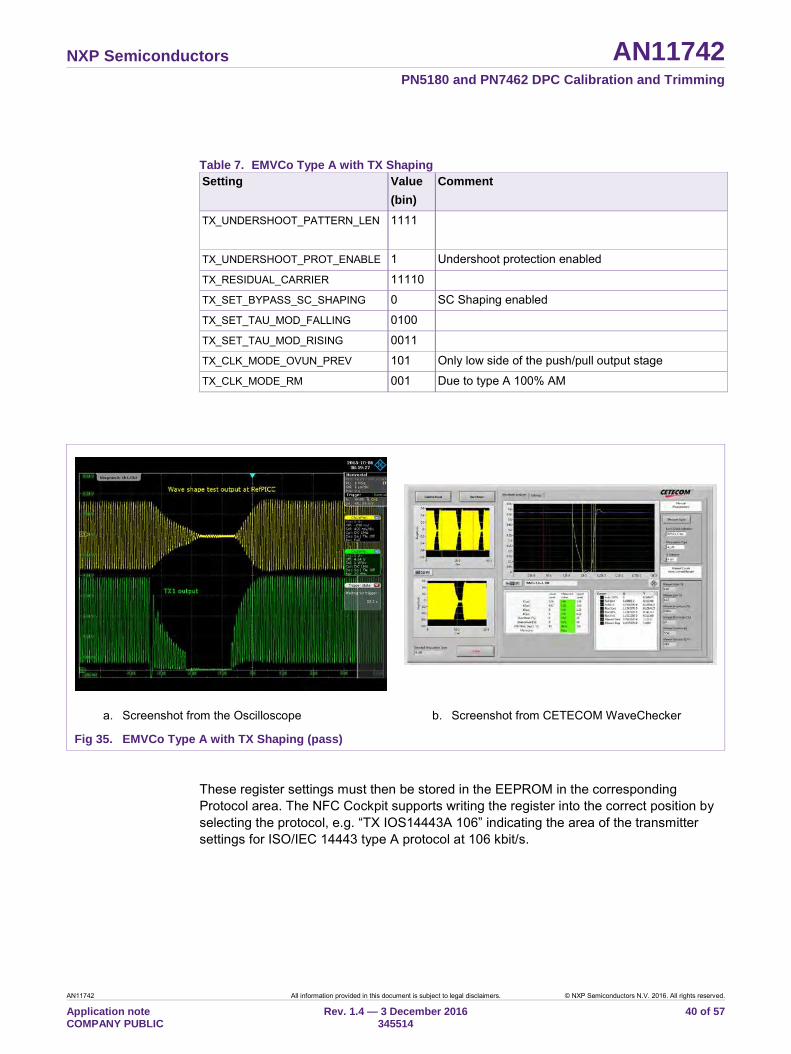
Fig 37. EMVCo Type B with TX Shaping (pass)
These register settings must then be stored in the EEPROM in the corresponding Protocol area. The NFC Cockpit supports writing the register into the correct position by selecting the protocol, e.g. “TX IOS14443B 106” indicating the area of the transmitter settings for ISO/IEC 14443 type B protocol at 106 kbit/s.
4.8 Tx Shaping per DPC gear per protocol (AWC) With the load protocol the related TX Shaping settings are loaded for the gear 0, i.e. the gear with the maximum output power.
Reducing the output power with any higher gear can change the pulse shape behavior due to two reasons:
• First of all the different gear settings result in different driver behavior, which slightly can change the envelope.
• Secondly the loading as such, which causes the gear change, influences the envelope due to the detuning and loading of the antenna.
Therefore the PN5180 (resp. PN7462) allows to adapt the TX Shaping with three parameters per gear and per protocol: 4. TX_TAU_MOD_FALLING 5. TX_TAU_MOD_RISING 6. TX_RESIDUAL_CARRIER
These three parameters can be changed for a gear >0. The parameters are defined and stored as delta values, which apply to the defined gear and all higher gears. Each delta value defines the delta from the previous lower gear.
This feature is called Automatic Waveshape Control (AWC).

NXP Semiconductors AN11742 PN5180 and PN7462 DPC Calibration and Trimming
AN11742 All information provided in this document is subject to legal disclaimers. © NXP Semiconductors N.V. 2016. All rights reserved.
Application note COMPANY PUBLIC
Rev. 1.4 — 3 December 2016 345514
43 of 57
4.8.1 Simple example of a delta value per gear An Example for one parameter and one protocol, using 5 gears is shown in Table 9. In this example the Load Protocol (e.g. for ISO/IEC 14443 type A @106) defines the TAUM_MOD_RISING to be 3.
Table 9. Simple example of TX shaping per gear Load Protocol value of TX_TAU_MOD_RISING = 3 (e.g. ISO14443 type A 106) Delta value for gear 1 = -2 Delta value for gear 3 = -1 Gear # Delta value TX_TAU_MOD_RISING 0 - (n.a.) 3
1 -2 1
2 0 1
3 -1 0
4 0 0
5 0 0
Interpretation: Using these example values means the PN5180 (resp. PN7462) uses the TX_TAU_MOD_RISING value of 3 for gear 0.
As soon as the PN5180 (resp. PN7462) switches from gear 0 to gear 1, it automatically reduces the TAU_MOD_RISING to 1.
Switching from gear 1 to gear 2 does not change the TAU_MOD_RISING, but switching from gear 2 to gear 3 makes the PN5180 (resp. PN7462) automatically reduce the TAU_MOD_RISING to 0. Switching to higher gears does not changes the value anymore, but switching back to 2 changes the TAU_MOD_RISING back to 1, and switching back to gear 0 makes the PN5180 (resp. PN7462) changing back to 3.
For this definition 2 entries are required.
4.8.2 Entry table for the Tx Shaping per gear The EEPROM content is structured in a table of up to 16 entries, as shown in Table 10. Every entry must use a gear number equal or larger than the gear number of the previous entry, otherwise the entry will be ignored.
Table 10. Entry table in the EEPROM Each entry contains 32 bit. Entry # Protocol bit mask
Bit 31 … 16 Residual carrier Bit 15 … 12
TAU_MOD_RISING Bit 11 … 8
TAU_MOD_FALLING Bit 7 …4
Gear number Bit 3…0
1 Defines the protocol, which will be effected by the defined change. Details see Table 11.
Defines the change of the residual carrier. Range: -7 … +7
Defines the rising edge of the pulse. Range: -7 …. +7
Defines the falling edge of the pulse. Range: -7 … +7
Defines the gear number, which will be effected by the defined change.
2
…
16
Each entry can define a set of delta values for all three parameters, and can link this set to a single gear and any protocol, as shown in Table 11.

NXP Semiconductors AN11742 PN5180 and PN7462 DPC Calibration and Trimming
AN11742 All information provided in this document is subject to legal disclaimers. © NXP Semiconductors N.V. 2016. All rights reserved.
Application note COMPANY PUBLIC
Rev. 1.4 — 3 December 2016 345514
44 of 57
Table 11. PCD Shaping entry definition Each entry contains 32 bit.
The example of Table 9 requires 2 entries in the EEPROM: one for gear 1, another one for gear 3.
4.9 AWC Tools for PN5180 and PN7462 Due to the different release plans of the two products the tool chain is not yet fully the same.
4.9.1 AWC in the NFC Cockpit (PN5180) In case of the PN5180 the NFC Cockpit supports the adjustment of the AWC, as shown in Fig 38. Refer to [4] for more details.
Note: The PN5180 FW 3.6 and higher provides a similar automatic adjustment of Rx settings per gear per protocol, which is not yet supported by the NFC Cockpit (2.4.7 or 2.4.10). The corresponding settings must be disabled to properly use the current NFC Cockpit properly, and then must be manually set afterwards.
bit # Definition 31 … 29 RFU, don’t use. Must be 0.
28 180003m3 Enabling a protocol enables the defined PCD shaping setting changes, as defined in bit 15 … 4 for the defined gear as defined in bit 3 … 0. One or more protocols can be enabled.
27 15693 @ASK100%
26 15693 @ASK10%
25 NFC type F @424
24 NFC type F @212
23 14443 type B @848
22 14443 type B @424
21 14443 type B @212
20 14443 type B @106
19 14443 type A @848
18 14443 type A @424
17 14443 type A @212
16 14443 type A @106
15 …12 Residual carrier Sign bit + 3 bit value
11 … 8 TAU_MOD_RISING Sign bit + 3 bit value
7 … 4 TAU_MOD_FALLING Sign bit + 3 bit value
3 … 0 Gear number Gear number 1 … 14

NXP Semiconductors AN11742 PN5180 and PN7462 DPC Calibration and Trimming
AN11742 All information provided in this document is subject to legal disclaimers. © NXP Semiconductors N.V. 2016. All rights reserved.
Application note COMPANY PUBLIC
Rev. 1.4 — 3 December 2016 345514
45 of 57
(1) Example for AWC setting in gear 1 for type B
Fig 38. AWC with PN5180 NFC Cockpit
4.9.2 AWC with Excel sheet (PN7462) For the PN7462 there is a configuration tool (Excel sheet) available, which generates the EEPROM content, as shown in Fig 39. The generated example byte stream with two entries (0x02010A010003090100) must be stored into the EEPROM 0x201368 … 0x2013a7.

NXP Semiconductors AN11742 PN5180 and PN7462 DPC Calibration and Trimming
AN11742 All information provided in this document is subject to legal disclaimers. © NXP Semiconductors N.V. 2016. All rights reserved.
Application note COMPANY PUBLIC
Rev. 1.4 — 3 December 2016 345514
46 of 57
(2) Only for the ISO/IEC 14443 A 106 kbit/s, the rise time is decreased at gear 1 by 2, and further decreased by 1 at gear 3.
Fig 39. Simple example of TX shaping per gear
4.9.3 Example with Tx Shaping Configuration per gear per protocol Changing the load by reducing the operating distance of the Reference PICC changes the gear and the envelope. Fig 40 shows the example using the default load protocol settings as defined in section 4.7.1, when the load is changed and the gear has switched from gear 0 to gear 1. It still passes, but the rise time t4 is very close to the limit. So it would be safe to reduce the rise time by changing the TAU_MOD_RISING.

NXP Semiconductors AN11742 PN5180 and PN7462 DPC Calibration and Trimming
AN11742 All information provided in this document is subject to legal disclaimers. © NXP Semiconductors N.V. 2016. All rights reserved.
Application note COMPANY PUBLIC
Rev. 1.4 — 3 December 2016 345514
47 of 57
c. Screenshot from the Oscilloscope d. Screenshot from CETECOM WaveChecker
Fig 40. Type A almost bad in gear 1
This can be done with the NFC Cockpit, i.e. reading the TX Shaping settings indicates that the TAU_MOD_RISING has been set to 3 as shown in Table 12.
Table 12. EMVCo Type A with TX Shaping (gear 0) Setting Value
(bin) Comment
TX_UNDERSHOOT_PATTERN_LEN
1111
TX_UNDERSHOOT_PROT_ENABLE 1
TX_RESIDUAL_CARRIER 11110
TX_SET_BYPASS_SC_SHAPING 0
TX_SET_TAU_MOD_FALLING 0100
TX_SET_TAU_MOD_RISING 0011 This parameter defines the rise time and should be reduced in gear 1.
TX_CLK_MODE_OVUN_PREV 101
TX_CLK_MODE_RM 001
Changing the TAU_MOD_RISING manually to 1 reduces the t4 from 0.44µs to 0.39µs, as shown in Fig 41.

NXP Semiconductors AN11742 PN5180 and PN7462 DPC Calibration and Trimming
AN11742 All information provided in this document is subject to legal disclaimers. © NXP Semiconductors N.V. 2016. All rights reserved.
Application note COMPANY PUBLIC
Rev. 1.4 — 3 December 2016 345514
48 of 57
e. Screenshot from the Oscilloscope f. Screenshot from CETECOM WaveChecker
Fig 41. Type A good in gear 1
The PN7462 PCD Shaping Configuration tool (Excel sheet) allows now to enter the first entry of TX Shaping parameter change per gear and protocol, as shown in Fig 42.
This entry is only valid for the ISO/IEC 14443 type A at 106 for gear 1 and all higher gears. It defines a decrease of TAU_MOD_RISING by 2, as soon as the PN7462 switches from gear 0 to gear 1. Switching back from gear 1 to gear 0 returns to the original value of TAU_MOD_RISING.
The Excel macro automatically generates the configuration string 0x01010A0100, which must be stored into the EEPROM starting at address 0x201368.

NXP Semiconductors AN11742 PN5180 and PN7462 DPC Calibration and Trimming
AN11742 All information provided in this document is subject to legal disclaimers. © NXP Semiconductors N.V. 2016. All rights reserved.
Application note COMPANY PUBLIC
Rev. 1.4 — 3 December 2016 345514
49 of 57
(3) This Excel generates the byte stream 0x01010A0100.
Fig 42. PN7462 PCD Shaping Configuration first entry
In the next step the same test is made with type B. The load protocol uses the settings as defined in section 4.7.2. (see Table 8). Changing from gear 0 to gear it turns out that the modulation index increases. It still passes the limits as shown in Fig 43g, but the modulation index (m = 13.5) is quite close to the limit of 14. So the TX_RESIDUAL_CARRIER can be reduced e.g. by 1, which reduces the modulation index (m = 12.8).

NXP Semiconductors AN11742 PN5180 and PN7462 DPC Calibration and Trimming
AN11742 All information provided in this document is subject to legal disclaimers. © NXP Semiconductors N.V. 2016. All rights reserved.
Application note COMPANY PUBLIC
Rev. 1.4 — 3 December 2016 345514
50 of 57
g. Screenshot from CETECOM WaveCheck h. Almost bad (m = 13.5)
i. Screenshot from CETECOM WaveCheck j. Good after correction (m = 12.8)
Fig 43. Type B gear 1
This required change must be added to the PCD Shaping Configuration tool as shown in Fig 44.
(4) The second entry uses the same gear 1, but defines different changes for a different protocol.
Fig 44. PN7462 PCD Shaping Configuration second entry
In the next steps the next gears are checked for each type A and B. For gear 2 e.g. the type B modulation should be further reduced to not get too close to the limit (refer to Fig 45). A decrease of the TX_RESIDUAL_CARRIER by 2 changes m = 13.6 into m = 12.3.
NXP Semiconductors AN11742 PN5180 and PN7462 DPC Calibration and Trimming
AN11742 All information provided in this document is subject to legal disclaimers. © NXP Semiconductors N.V. 2016. All rights reserved.
Application note COMPANY PUBLIC
Rev. 1.4 — 3 December 2016 345514
51 of 57
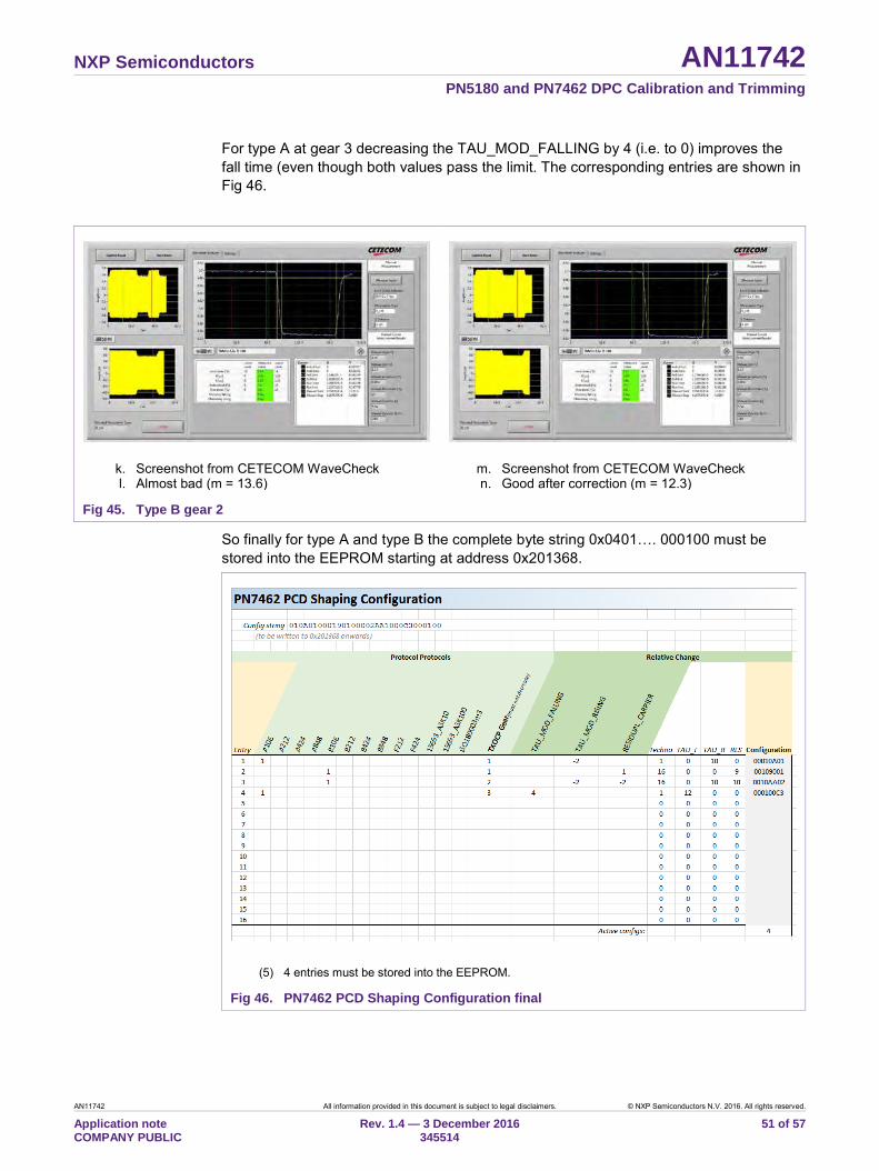
For type A at gear 3 decreasing the TAU_MOD_FALLING by 4 (i.e. to 0) improves the fall time (even though both values pass the limit. The corresponding entries are shown in Fig 46.
k. Screenshot from CETECOM WaveCheck l. Almost bad (m = 13.6)
m. Screenshot from CETECOM WaveCheck n. Good after correction (m = 12.3)
Fig 45. Type B gear 2
So finally for type A and type B the complete byte string 0x0401…. 000100 must be stored into the EEPROM starting at address 0x201368.
(5) 4 entries must be stored into the EEPROM.
Fig 46. PN7462 PCD Shaping Configuration final
NXP Semiconductors AN11742 PN5180 and PN7462 DPC Calibration and Trimming
AN11742 All information provided in this document is subject to legal disclaimers. © NXP Semiconductors N.V. 2016. All rights reserved.
Application note COMPANY PUBLIC
Rev. 1.4 — 3 December 2016 345514
52 of 57
5. Trim Procedure Each production device must be trimmed with a device specific DPC_XI value. This should be done during the device testing after production.
Trim procedure steps for each production device:
1) Load the Reference EEPROM values into the EEPROM.
2) Load Protocol (e.g. for type A 106).
3) Enable the RF field, no loading applied.
4) Read RF_STATUS. If gear >0, then
a. Read DPC_AGC_GEAR_LUT_SIZE
b. Write 0x01 into DPC_AGC_GEAR_LUT_SIZE to force the device into gear 0
c. Reset RF Field
d. Read RF_STATUS
e. Restore DPC_AGC_GEAR_LUT_SIZE to previous value.
5) Calculate the DPC_XI value:
DPC_XI value = Reference AGC value (from “golden device”) – current AGC value (bit 0…9 from RF_STATUS)
6) Write DPC_XI value into DPC_XI EEPROM.
7) Perform SoftReset, in case the correct DPC function shall be tested immediately.
Note: After the trim procedure the DPC must switch gear at the same ITVDD limit like the Reference device.
6. References [1] AN11740 PN5180 antenna design guide, www.nxp.com
[2] AN11741 How to design an antenna with DPC, www.nxp.com
[3] UM10858 PN7462 HW user manual, www.nxp.com
[4] AN11744 PN5180 Evaluation Board quick start guide, www.nxp.com

NXP Semiconductors AN11742 PN5180 and PN7462 DPC Calibration and Trimming
AN11742 All information provided in this document is subject to legal disclaimers. © NXP Semiconductors N.V. 2016. All rights reserved.
Application note COMPANY PUBLIC
Rev. 1.4 — 3 December 2016 345514
53 of 57
7. Annex Example measurement of AGC values per gear of the same antenna like the example antenna from [2], using the same DPC antenna tuning. However, here the AGC values are lower, since a higher Rx coupling resistor has been used.
Table 13. Example measurement of DPC_THRSH_HIGH The Rx resistor = 5.1kΩ, so the nominal AGC value unloaded is too low. Gear # AGC (hex) AGC (dec) Loading ITVDD 0 0F3 243 (should be 300) Unloaded 139
0 140 320 1 180
1 10C 268 1 151
1 13B 315 2 180
2 0FC 252 2 141
2 140 320 3 180
3 0D6 214 3 122
3 124 292 4 180
4 03B 59 4 75
4 04D 77 5 76

NXP Semiconductors AN11742 PN5180 and PN7462 DPC Calibration and Trimming
AN11742 All information provided in this document is subject to legal disclaimers. © NXP Semiconductors N.V. 2016. All rights reserved.
Application note COMPANY PUBLIC
Rev. 1.4 — 3 December 2016 345514
54 of 57
8. Legal information
8.1 Definitions Draft — The document is a draft version only. The content is still under internal review and subject to formal approval, which may result in modifications or additions. NXP Semiconductors does not give any representations or warranties as to the accuracy or completeness of information included herein and shall have no liability for the consequences of use of such information.
8.2 Disclaimers Limited warranty and liability — Information in this document is believed to be accurate and reliable. However, NXP Semiconductors does not give any representations or warranties, expressed or implied, as to the accuracy or completeness of such information and shall have no liability for the consequences of use of such information. NXP Semiconductors takes no responsibility for the content in this document if provided by an information source outside of NXP Semiconductors.
In no event shall NXP Semiconductors be liable for any indirect, incidental, punitive, special or consequential damages (including - without limitation - lost profits, lost savings, business interruption, costs related to the removal or replacement of any products or rework charges) whether or not such damages are based on tort (including negligence), warranty, breach of contract or any other legal theory.
Notwithstanding any damages that customer might incur for any reason whatsoever, NXP Semiconductors’ aggregate and cumulative liability towards customer for the products described herein shall be limited in accordance with the Terms and conditions of commercial sale of NXP Semiconductors.
Right to make changes — NXP Semiconductors reserves the right to make changes to information published in this document, including without limitation specifications and product descriptions, at any time and without notice. This document supersedes and replaces all information supplied prior to the publication hereof.
Suitability for use — NXP Semiconductors products are not designed, authorized or warranted to be suitable for use in life support, life-critical or safety-critical systems or equipment, nor in applications where failure or malfunction of an NXP Semiconductors product can reasonably be expected to result in personal injury, death or severe property or environmental damage. NXP Semiconductors and its suppliers accept no liability for inclusion and/or use of NXP Semiconductors products in such equipment or applications and therefore such inclusion and/or use is at the customer’s own risk.
Applications — Applications that are described herein for any of these products are for illustrative purposes only. NXP Semiconductors makes no representation or warranty that such applications will be suitable for the specified use without further testing or modification.
Customers are responsible for the design and operation of their applications and products using NXP Semiconductors products, and NXP Semiconductors accepts no liability for any assistance with applications or customer product design. It is customer’s sole responsibility to determine whether the NXP Semiconductors product is suitable and fit for the customer’s applications and products planned, as well as for the planned application and use of customer’s third party customer(s). Customers should provide appropriate design and operating safeguards to minimize the risks associated with their applications and products.
NXP Semiconductors does not accept any liability related to any default, damage, costs or problem which is based on any weakness or default in the customer’s applications or products, or the application or use by customer’s third party customer(s). Customer is responsible for doing all necessary testing for the customer’s applications and products using NXP Semiconductors products in order to avoid a default of the applications and the products or of the application or use by customer’s third party customer(s). NXP does not accept any liability in this respect.
Export control — This document as well as the item(s) described herein may be subject to export control regulations. Export might require a prior authorization from competent authorities.
Translations — A non-English (translated) version of a document is for reference only. The English version shall prevail in case of any discrepancy between the translated and English versions.
Evaluation products — This product is provided on an “as is” and “with all faults” basis for evaluation purposes only. NXP Semiconductors, its affiliates and their suppliers expressly disclaim all warranties, whether express, implied or statutory, including but not limited to the implied warranties of non-infringement, merchantability and fitness for a particular purpose. The entire risk as to the quality, or arising out of the use or performance, of this product remains with customer.
In no event shall NXP Semiconductors, its affiliates or their suppliers be liable to customer for any special, indirect, consequential, punitive or incidental damages (including without limitation damages for loss of business, business interruption, loss of use, loss of data or information, and the like) arising out the use of or inability to use the product, whether or not based on tort (including negligence), strict liability, breach of contract, breach of warranty or any other theory, even if advised of the possibility of such damages.
Notwithstanding any damages that customer might incur for any reason whatsoever (including without limitation, all damages referenced above and all direct or general damages), the entire liability of NXP Semiconductors, its affiliates and their suppliers and customer’s exclusive remedy for all of the foregoing shall be limited to actual damages incurred by customer based on reasonable reliance up to the greater of the amount actually paid by customer for the product or five dollars (US$5.00). The foregoing limitations, exclusions and disclaimers shall apply to the maximum extent permitted by applicable law, even if any remedy fails of its essential purpose.
8.3 Licenses Purchase of NXP ICs with NFC technology
Purchase of an NXP Semiconductors IC that complies with one of the Near Field Communication (NFC) standards ISO/IEC 18092 and ISO/IEC 21481 does not convey an implied license under any patent right infringed by implementation of any of those standards. Purchase of NXP Semiconductors IC does not include a license to any NXP patent (or other IP right) covering combinations of those products with other products, whether hardware or software.
8.4 Trademarks Notice: All referenced brands, product names, service names and trademarks are property of their respective owners.
MIFARE — is a trademark of NXP B.V.
NXP Semiconductors AN11742 PN5180 and PN7462 DPC Calibration and Trimming
AN11742 All information provided in this document is subject to legal disclaimers. © NXP Semiconductors N.V. 2016. All rights reserved.
Application note COMPANY PUBLIC
Rev. 1.4 — 3 December 2016 345514
55 of 57
9. List of figures
Fig 1. Loading of a typical DPC antenna tuning .......... 4 Fig 2. DPC principle .................................................... 5 Fig 3. DPC Gears in principle ..................................... 6 Fig 4. RF Field on with DPC ....................................... 8 Fig 5. TX Power setting bit 0…3 ................................. 9 Fig 6. Example of ITVDD versus Gear ...................... 11 Fig 7. Correlation between AGC and ITVDD ............ 15 Fig 8. Correlation example ........................................ 16 Fig 9. Jumper of the PN5180 Evaluation board ........ 17 Fig 10. Jumper of the PN7462 Evaluation board ........ 18 Fig 11. Correlation test steps 1…4.............................. 19 Fig 12. Correlation test step 5 ..................................... 20 Fig 13. Correlation test start of second loading case .. 21 Fig 14. Correlation test last step ................................. 22 Fig 15. Correlation test result ...................................... 23 Fig 16. DPC Calibration Step 1 ................................... 24 Fig 17. DPC Calibration Step 2 ................................... 25 Fig 18. DPC Calibration Step 3 ................................... 25 Fig 19. DPC Calibration start with gear 0 .................... 26 Fig 20. DPC Calibration finish gear 0 .......................... 27 Fig 21. DPC calibration with gear 1............................. 27 Fig 22. DPC calibration storing the DPC settings........ 28 Fig 23. PN5180 Type A pulse, no shaping .................. 29 Fig 24. Tx Shaping principle 1 .................................... 30 Fig 25. Tx Shaping principle 2 .................................... 30 Fig 26. TX shaping test setup ..................................... 31 Fig 27. TX undershoot patter length............................ 34 Fig 28. TX Undershoot pattern .................................... 34 Fig 29. TX undershoot residual carrier ........................ 35 Fig 30. TX Overshoot Residual carrier ....................... 35 Fig 31. TX undershoot Fall time behavior ................... 36 Fig 32. TX overshoot Rise time behavior .................... 36 Fig 33. Example antenna ............................................ 39 Fig 34. EMVCo Type A without TX Shaping (fail) ....... 39 Fig 35. EMVCo Type A with TX Shaping (pass) ......... 40 Fig 36. EMVCo Type B without TX Shaping (fail) ....... 41 Fig 37. EMVCo Type B with TX Shaping (pass) ......... 42 Fig 38. AWC with PN5180 NFC Cockpit ..................... 45 Fig 39. Simple example of TX shaping per gear ......... 46 Fig 40. Type A almost bad in gear 1 ........................... 47 Fig 41. Type A good in gear 1 ..................................... 48 Fig 42. PN7462 PCD Shaping Configuration first
entry ................................................................ 49 Fig 43. Type B gear 1 ................................................. 50 Fig 44. PN7462 PCD Shaping Configuration second
entry ................................................................ 50
Fig 45. Type B gear 2 .................................................. 51 Fig 46. PN7462 PCD Shaping Configuration final ....... 51

NXP Semiconductors AN11742 PN5180 and PN7462 DPC Calibration and Trimming
AN11742 All information provided in this document is subject to legal disclaimers. © NXP Semiconductors N.V. 2016. All rights reserved.
Application note COMPANY PUBLIC
Rev. 1.4 — 3 December 2016 345514
56 of 57
10. List of tables
Table 1. Relevant parameters of the DPC (PN5180) ...... 6 Table 2. TX Power Settings (bit 7...0) ............................. 9 Table 3. Example of Tx Output settings (15 gears) ....... 10 Table 4. Example of Tx Output power settings
(5 gears).......................................................... 10 Table 5. Example measurement of
DPC_THRSH_HIGH ....................................... 12 Table 6. Example PN5180 EEPROM content for
DPC_THRSH_HIGH ....................................... 13 Table 7. EMVCo Type A with TX Shaping .................... 40 Table 8. EMVCo Type B with TX Shaping .................... 41 Table 9. Simple example of TX shaping per gear ......... 43 Table 10. Entry table in the EEPROM............................. 43 Table 11. PCD Shaping entry definition .......................... 44 Table 12. EMVCo Type A with TX Shaping (gear 0) ....... 47 Table 13. Example measurement of
DPC_THRSH_HIGH ....................................... 53
NXP Semiconductors AN11742 PN5180 and PN7462 DPC Calibration and Trimming
Please be aware that important notices concerning this document and the product(s) described herein, have been included in the section 'Legal information'.
© NXP Semiconductors N.V. 2016. All rights reserved.
For more information, visit: http://www.nxp.com
Date of release: 3 December 2016 345514
Document identifier: AN11742
11. Contents
1. Introduction ......................................................... 3 1.1 The principle of DPC .......................................... 4 1.2 Parameters of DPC ............................................ 6 1.2.1 DPC_CONTROL ................................................ 7 1.2.1.1 Bit 0: Enable DPC .............................................. 7 1.2.1.2 Bit 1…3: Gear step size ..................................... 7 1.2.1.3 Bit 4…7: Start gear ............................................. 7 1.2.2 DPC_AGC_GEAR_LUT_SIZE ........................... 7 1.2.3 DPC_AGC_GEAR_LUT (TX Output power
settings).............................................................. 8 1.2.4 DPC_THRSH_HIGH ........................................ 11 1.2.4.1 DPC_THRS_HIGH Example with 5 gears ........ 12 1.2.5 DPC_AGC_SHIFT_VALUE .............................. 13 1.2.6 DPC_XI ............................................................ 14 1.2.6.1 Define Reference AGC value ........................... 14 1.2.6.2 Trim production device ..................................... 14 2. DPC Correlation test ......................................... 15 2.1 Correlation test ................................................. 15 2.2 Correlation test with the NFC Cockpit .............. 16 2.2.1 PN5180 ............................................................ 16 2.2.2 PN7462 ............................................................ 17 2.2.3 Step 1: ITVDD unloaded .................................. 18 2.2.4 Step 2: Step size .............................................. 19 2.2.5 Step 3: ITVDD max .......................................... 19 2.2.6 Step 4: Start correlation test ............................. 19 2.2.7 Step 5: ITVDD / AGC measurement loading
case 1 .............................................................. 20 2.2.8 Step 6: ITVDD / AGC measurement loading
case 2 .............................................................. 21 2.2.9 Step 7: Store the result .................................... 22 3. DPC calibration .................................................. 23 3.1 Prerequisites .................................................... 23 3.2 DPC Calibration minimum requirements .......... 23 3.3 Calibration procedure with the NFC Cockpit .... 24 4. Tx Shaping ......................................................... 29 4.1 Tx Shaping principle ......................................... 29 4.2 Wave shape test set up .................................... 31 4.3 Differences PN5180 versus PN7462 ................ 32 4.3.1 PN5180 relevant registers ................................ 32 4.3.2 PN7462 relevant registers ................................ 32 4.4 PN5180 and PN7462 relevant settings ............ 33 4.4.1.1 TX_UNDERSHOOT_PROT_ENABLE ............. 33 4.4.1.2 TX_UNDERSHOOT_PATTERN_LEN ............. 33 4.4.2 TX_UNDERSHOOT_PATTERN ...................... 34 4.4.2.1 TX_RESIDUAL_CARRIER............................... 34 4.4.2.2 TX_SET_BYPASS_SC_SHAPING .................. 35
4.4.2.3 TX_SET_TAU_MOD_FALLING ....................... 35 4.4.2.4 TX_SET_TAU_MOD_RISING .......................... 36 4.4.2.5 TX_CLK_MODE_OVUN_PREV ....................... 36 4.5 Remove undershoot ......................................... 37 4.6 Remove overshoot ........................................... 38 4.7 Examples .......................................................... 39 4.7.1 Example of a TX shaping setting for type A ...... 39 4.7.2 Example of a TX shaping setting for type B ...... 41 4.8 Tx Shaping per DPC gear per protocol (AWC) . 42 4.8.1 Simple example of a delta value per gear ........ 43 4.8.2 Entry table for the Tx Shaping per gear ............ 43 4.9 AWC Tools for PN5180 and PN7462 ............... 44 4.9.1 AWC in the NFC Cockpit (PN5180) .................. 44 4.9.2 AWC with Excel sheet (PN7462) ...................... 45 4.9.3 Example with Tx Shaping Configuration per gear
per protocol ...................................................... 46 5. Trim Procedure .................................................. 52 6. References ......................................................... 52 7. Annex.................................................................. 53 8. Legal information .............................................. 54 8.1 Definitions ......................................................... 54 8.2 Disclaimers ....................................................... 54 8.3 Licenses ........................................................... 54 8.4 Trademarks ...................................................... 54 9. List of figures ..................................................... 55 10. List of tables ...................................................... 56 11. Contents ............................................................. 57