Embed Size (px)
Citation preview
Semiconductor Components Industries, LLC, 2001
April, 2001– Rev. 31 Publication Order Number:
AN1650/D
AN1650/D
Using WireOR Ties inECLinPS Designs
This application note discusses the use of wire-OR ties in EClinPS designs. Theoretical Descriptions of the problemsassociated with wire-OR ties are included as well as an evaluation and SPICE simulation results. In addition, general guidelinesand recommendations are provided to assist the system designer in successfully using wire-OR ties in ECLinPS designs.
INTRODUCTION
The use of wired-OR connections in ECL designs is apopular way to reduce the total part count and optimize thespeed performance of a system. The limitations of OR-tyingECL outputs has always been a combination of increaseddelay per OR-tie, and the negative going disturbance seen atthe output when one output switches from a high to a lowstate while the rest of the outputs remain high. As the speedof the output transition times increase, the latter problembecomes the primary limitation on the practice of OR-tyingECL outputs. This fact is due to the sensitivity of thisphenomena to decreasing output transition times.
This application note will address the practice ofOR-tying outputs in the implementation of designs using theECLinPS family of logic devices. A theoretical descriptionof the problem, as well as evaluation and simulation results,will be presented. In addition, guidelines will be offeredwhich, if followed, will help to ensure the desired operationof ECLinPS designs using wired-OR outputs.
THEORETICAL DESCRIPTION
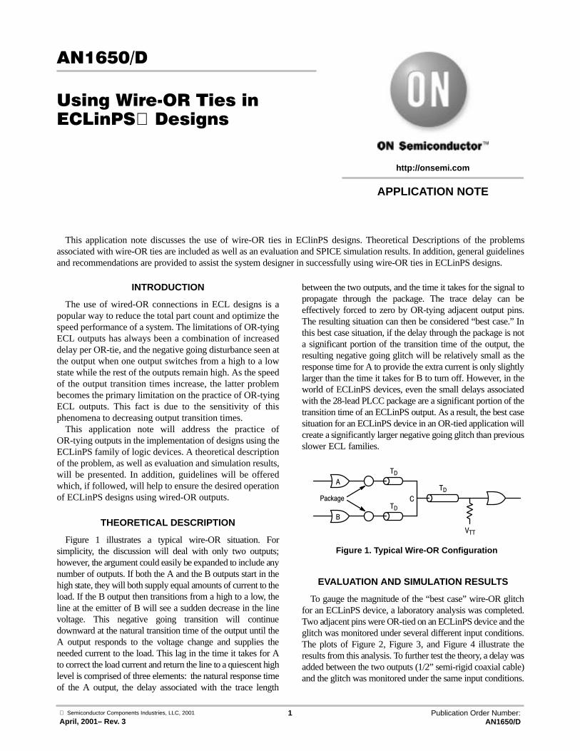
Figure 1 illustrates a typical wire-OR situation. Forsimplicity, the discussion will deal with only two outputs;however, the argument could easily be expanded to include anynumber of outputs. If both the A and the B outputs start in thehigh state, they will both supply equal amounts of current to theload. If the B output then transitions from a high to a low, theline at the emitter of B will see a sudden decrease in the linevoltage. This negative going transition will continuedownward at the natural transition time of the output until theA output responds to the voltage change and supplies theneeded current to the load. This lag in the time it takes for Ato correct the load current and return the line to a quiescent highlevel is comprised of three elements: the natural response timeof the A output, the delay associated with the trace length
between the two outputs, and the time it takes for the signal topropagate through the package. The trace delay can beeffectively forced to zero by OR-tying adjacent output pins.The resulting situation can then be considered “best case.” Inthis best case situation, if the delay through the package is nota significant portion of the transition time of the output, theresulting negative going glitch will be relatively small as theresponse time for A to provide the extra current is only slightlylarger than the time it takes for B to turn off. However, in theworld of ECLinPS devices, even the small delays associatedwith the 28-lead PLCC package are a significant portion of thetransition time of an ECLinPS output. As a result, the best casesituation for an ECLinPS device in an OR-tied application willcreate a significantly larger negative going glitch than previousslower ECL families.
Figure 1. Typical Wire-OR Configuration
TDA
TD
Package
B
TD
VTT
C
EVALUATION AND SIMULATION RESULTS
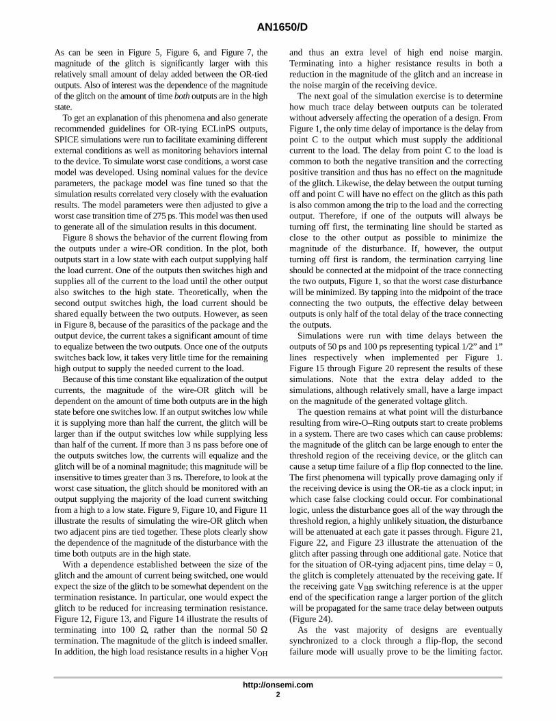
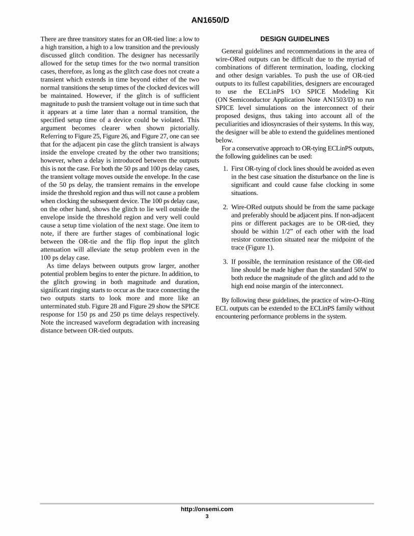
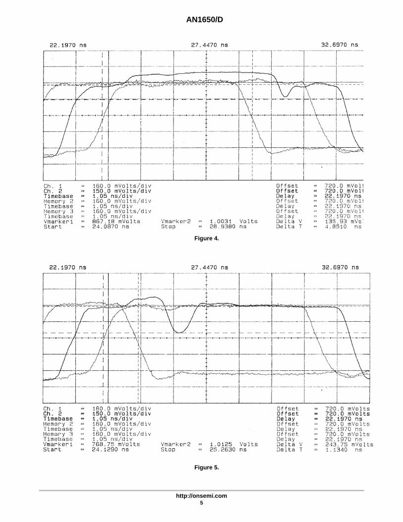
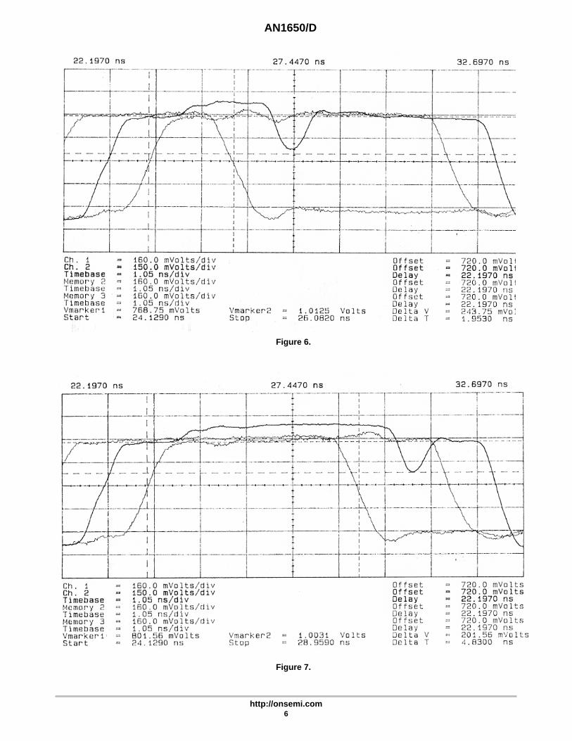
To gauge the magnitude of the “best case” wire-OR glitchfor an ECLinPS device, a laboratory analysis was completed.Two adjacent pins were OR-tied on an ECLinPS device and theglitch was monitored under several different input conditions.The plots of Figure 2, Figure 3, and Figure 4 illustrate theresults from this analysis. To further test the theory, a delay wasadded between the two outputs (1/2” semi-rigid coaxial cable)and the glitch was monitored under the same input conditions.
http://onsemi.com
APPLICATION NOTE
AN1650/D
http://onsemi.com2
As can be seen in Figure 5, Figure 6, and Figure 7, themagnitude of the glitch is significantly larger with thisrelatively small amount of delay added between the OR-tiedoutputs. Also of interest was the dependence of the magnitudeof the glitch on the amount of time both outputs are in the highstate.
To get an explanation of this phenomena and also generaterecommended guidelines for OR-tying ECLinPS outputs,SPICE simulations were run to facilitate examining differentexternal conditions as well as monitoring behaviors internalto the device. To simulate worst case conditions, a worst casemodel was developed. Using nominal values for the deviceparameters, the package model was fine tuned so that thesimulation results correlated very closely with the evaluationresults. The model parameters were then adjusted to give aworst case transition time of 275 ps. This model was then usedto generate all of the simulation results in this document.
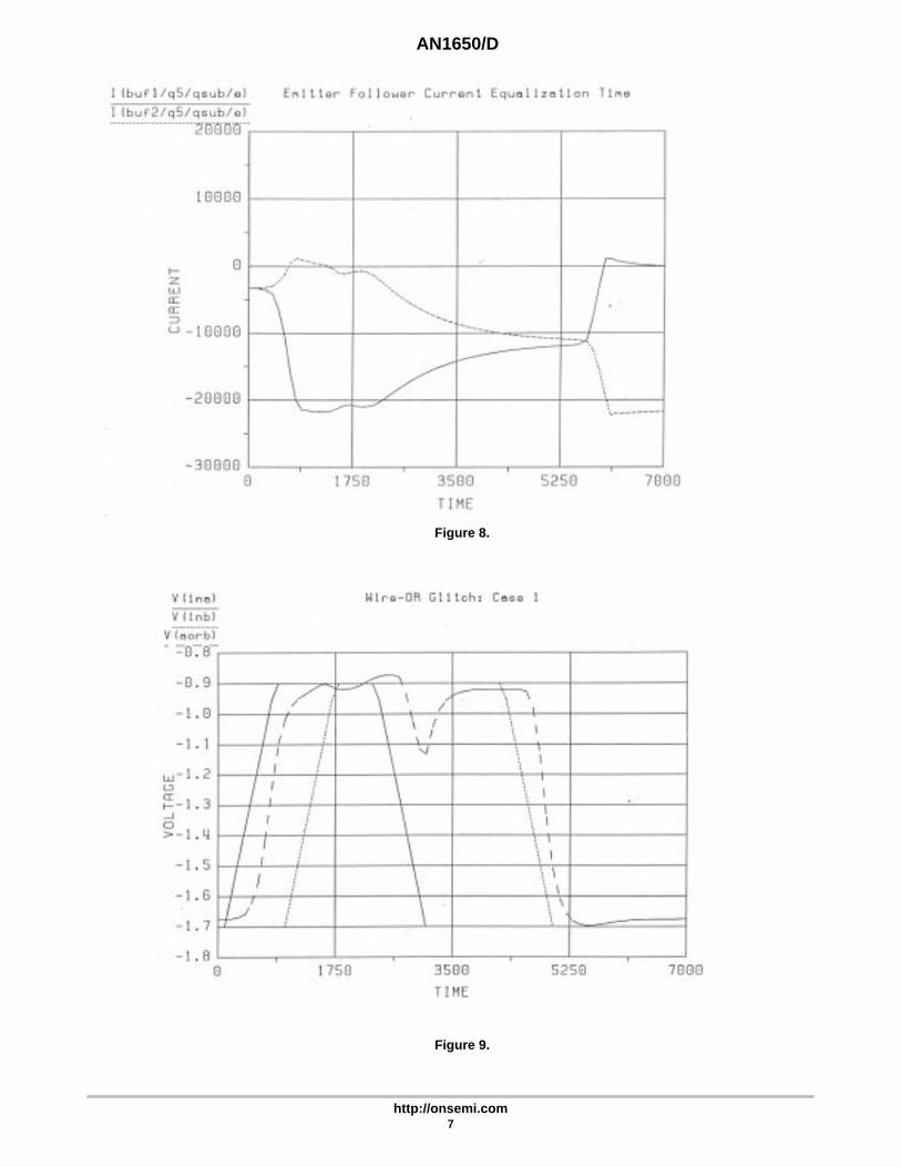
Figure 8 shows the behavior of the current flowing fromthe outputs under a wire-OR condition. In the plot, bothoutputs start in a low state with each output supplying halfthe load current. One of the outputs then switches high andsupplies all of the current to the load until the other outputalso switches to the high state. Theoretically, when thesecond output switches high, the load current should beshared equally between the two outputs. However, as seenin Figure 8, because of the parasitics of the package and theoutput device, the current takes a significant amount of timeto equalize between the two outputs. Once one of the outputsswitches back low, it takes very little time for the remaininghigh output to supply the needed current to the load.
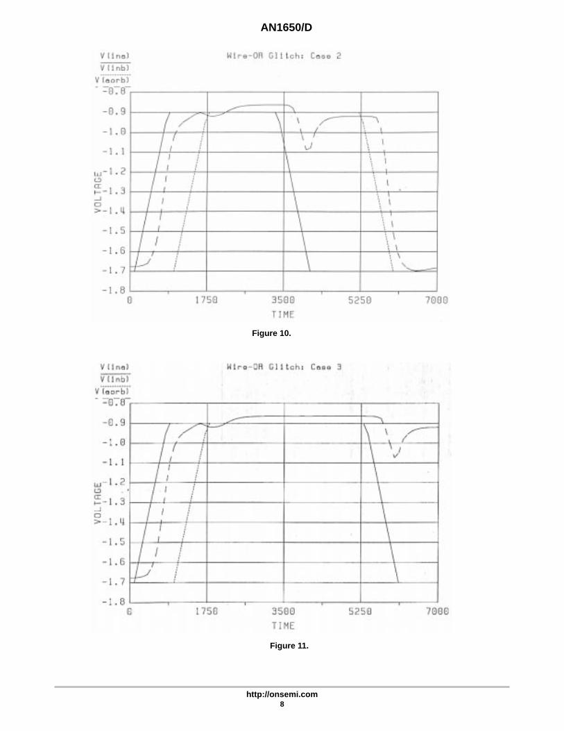
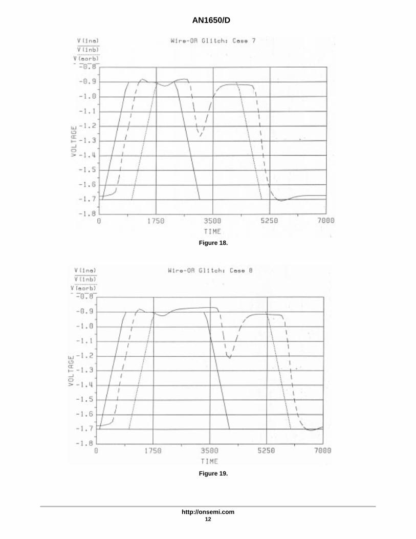
Because of this time constant like equalization of the outputcurrents, the magnitude of the wire-OR glitch will bedependent on the amount of time both outputs are in the highstate before one switches low. If an output switches low whileit is supplying more than half the current, the glitch will belarger than if the output switches low while supplying lessthan half of the current. If more than 3 ns pass before one ofthe outputs switches low, the currents will equalize and theglitch will be of a nominal magnitude; this magnitude will beinsensitive to times greater than 3 ns. Therefore, to look at theworst case situation, the glitch should be monitored with anoutput supplying the majority of the load current switchingfrom a high to a low state. Figure 9, Figure 10, and Figure 11illustrate the results of simulating the wire-OR glitch whentwo adjacent pins are tied together. These plots clearly showthe dependence of the magnitude of the disturbance with thetime both outputs are in the high state.
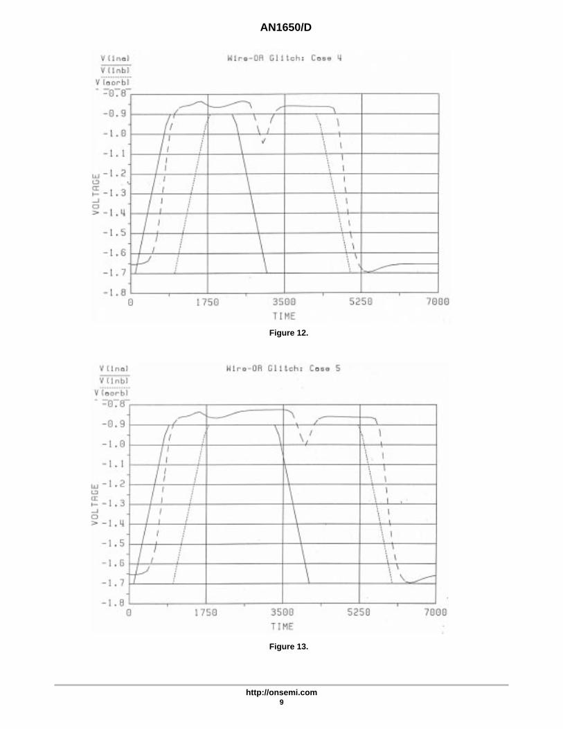
With a dependence established between the size of theglitch and the amount of current being switched, one wouldexpect the size of the glitch to be somewhat dependent on thetermination resistance. In particular, one would expect theglitch to be reduced for increasing termination resistance.Figure 12, Figure 13, and Figure 14 illustrate the results ofterminating into 100 Ω, rather than the normal 50 Ωtermination. The magnitude of the glitch is indeed smaller.In addition, the high load resistance results in a higher VOH
and thus an extra level of high end noise margin.Terminating into a higher resistance results in both areduction in the magnitude of the glitch and an increase inthe noise margin of the receiving device.
The next goal of the simulation exercise is to determinehow much trace delay between outputs can be toleratedwithout adversely affecting the operation of a design. FromFigure 1, the only time delay of importance is the delay frompoint C to the output which must supply the additionalcurrent to the load. The delay from point C to the load iscommon to both the negative transition and the correctingpositive transition and thus has no effect on the magnitudeof the glitch. Likewise, the delay between the output turningoff and point C will have no effect on the glitch as this pathis also common among the trip to the load and the correctingoutput. Therefore, if one of the outputs will always beturning off first, the terminating line should be started asclose to the other output as possible to minimize themagnitude of the disturbance. If, however, the outputturning off first is random, the termination carrying lineshould be connected at the midpoint of the trace connectingthe two outputs, Figure 1, so that the worst case disturbancewill be minimized. By tapping into the midpoint of the traceconnecting the two outputs, the effective delay betweenoutputs is only half of the total delay of the trace connectingthe outputs.
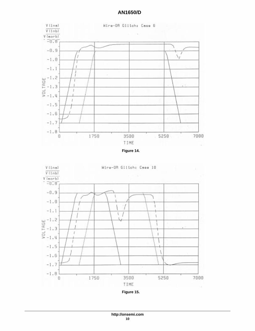
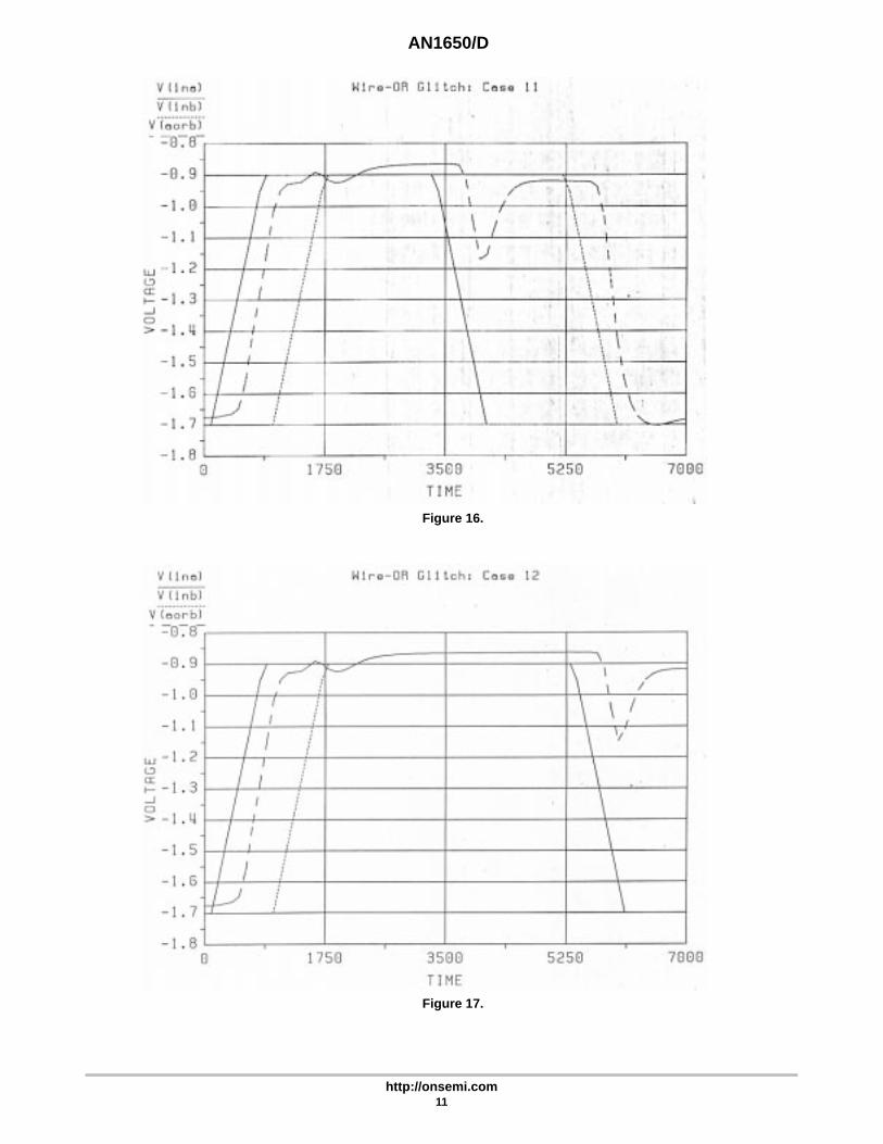
Simulations were run with time delays between theoutputs of 50 ps and 100 ps representing typical 1/2” and 1”lines respectively when implemented per Figure 1.Figure 15 through Figure 20 represent the results of thesesimulations. Note that the extra delay added to thesimulations, although relatively small, have a large impacton the magnitude of the generated voltage glitch.
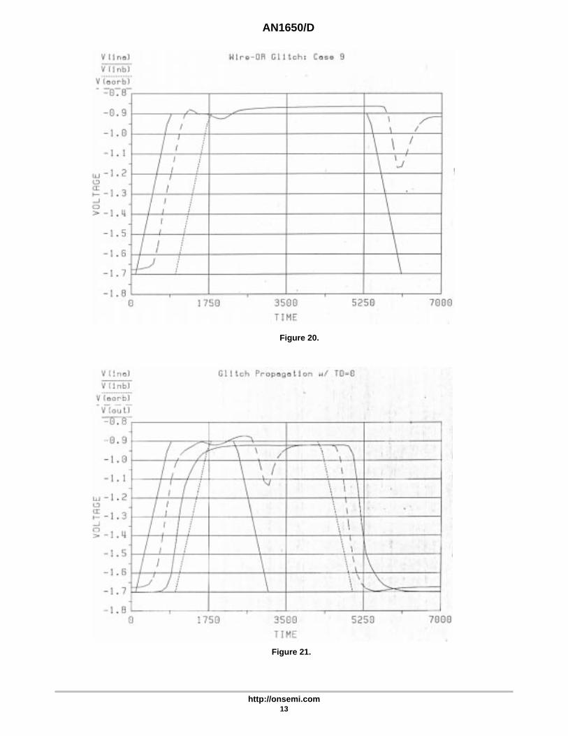
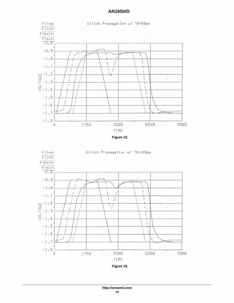
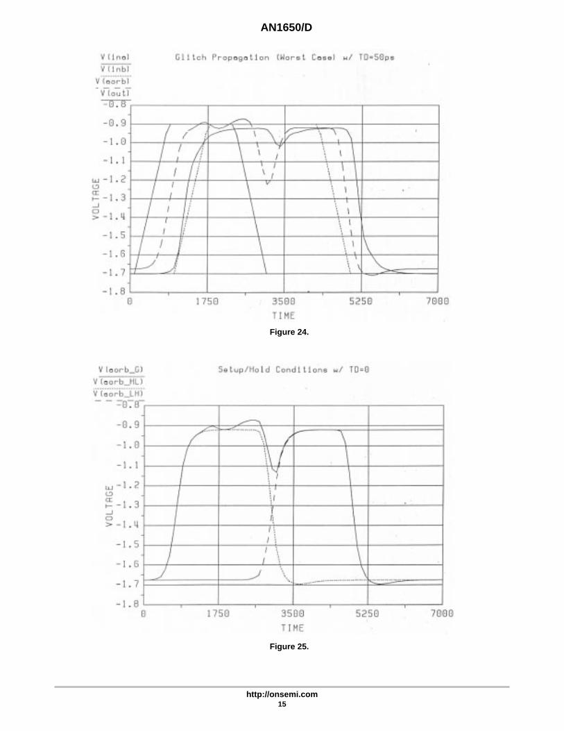
The question remains at what point will the disturbanceresulting from wire-O–Ring outputs start to create problemsin a system. There are two cases which can cause problems:the magnitude of the glitch can be large enough to enter thethreshold region of the receiving device, or the glitch cancause a setup time failure of a flip flop connected to the line.The first phenomena will typically prove damaging only ifthe receiving device is using the OR-tie as a clock input; inwhich case false clocking could occur. For combinationallogic, unless the disturbance goes all of the way through thethreshold region, a highly unlikely situation, the disturbancewill be attenuated at each gate it passes through. Figure 21,Figure 22, and Figure 23 illustrate the attenuation of theglitch after passing through one additional gate. Notice thatfor the situation of OR-tying adjacent pins, time delay = 0,the glitch is completely attenuated by the receiving gate. Ifthe receiving gate VBB switching reference is at the upperend of the specification range a larger portion of the glitchwill be propagated for the same trace delay between outputs(Figure 24).
As the vast majority of designs are eventuallysynchronized to a clock through a flip-flop, the secondfailure mode will usually prove to be the limiting factor.
AN1650/D
http://onsemi.com3
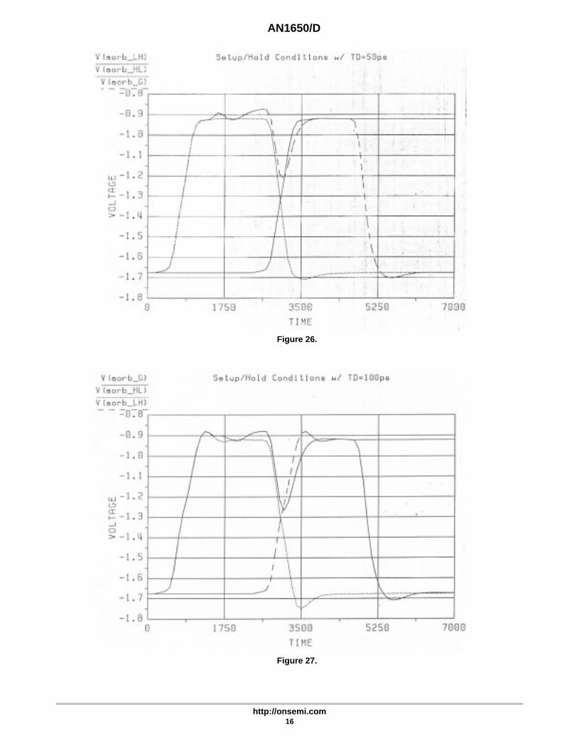
There are three transitory states for an OR-tied line: a low toa high transition, a high to a low transition and the previouslydiscussed glitch condition. The designer has necessarilyallowed for the setup times for the two normal transitioncases, therefore, as long as the glitch case does not create atransient which extends in time beyond either of the twonormal transitions the setup times of the clocked devices willbe maintained. However, if the glitch is of sufficientmagnitude to push the transient voltage out in time such thatit appears at a time later than a normal transition, thespecified setup time of a device could be violated. Thisargument becomes clearer when shown pictorially.Referring to Figure 25, Figure 26, and Figure 27, one can seethat for the adjacent pin case the glitch transient is alwaysinside the envelope created by the other two transitions;however, when a delay is introduced between the outputsthis is not the case. For both the 50 ps and 100 ps delay cases,the transient voltage moves outside the envelope. In the caseof the 50 ps delay, the transient remains in the envelopeinside the threshold region and thus will not cause a problemwhen clocking the subsequent device. The 100 ps delay case,on the other hand, shows the glitch to lie well outside theenvelope inside the threshold region and very well couldcause a setup time violation of the next stage. One item tonote, if there are further stages of combinational logicbetween the OR-tie and the flip flop input the glitchattenuation will alleviate the setup problem even in the100 ps delay case.
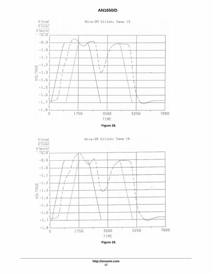
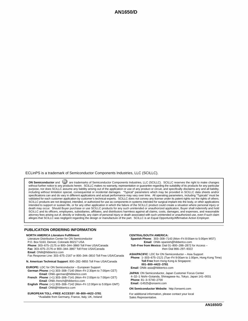
As time delays between outputs grow larger, anotherpotential problem begins to enter the picture. In addition, tothe glitch growing in both magnitude and duration,significant ringing starts to occur as the trace connecting thetwo outputs starts to look more and more like anunterminated stub. Figure 28 and Figure 29 show the SPICEresponse for 150 ps and 250 ps time delays respectively.Note the increased waveform degradation with increasingdistance between OR-tied outputs.
DESIGN GUIDELINES
General guidelines and recommendations in the area ofwire-ORed outputs can be difficult due to the myriad ofcombinations of different termination, loading, clockingand other design variables. To push the use of OR-tiedoutputs to its fullest capabilities, designers are encouragedto use the ECLinPS I/O SPICE Modeling Kit(ON Semiconductor Application Note AN1503/D) to runSPICE level simulations on the interconnect of theirproposed designs, thus taking into account all of thepeculiarities and idiosyncrasies of their systems. In this way,the designer will be able to extend the guidelines mentionedbelow.
For a conservative approach to OR-tying ECLinPS outputs,the following guidelines can be used:
1. First OR-tying of clock lines should be avoided as evenin the best case situation the disturbance on the line issignificant and could cause false clocking in somesituations.
2. Wire-ORed outputs should be from the same packageand preferably should be adjacent pins. If non-adjacentpins or different packages are to be OR-tied, theyshould be within 1/2” of each other with the loadresistor connection situated near the midpoint of thetrace (Figure 1).
3. If possible, the termination resistance of the OR-tiedline should be made higher than the standard 50W toboth reduce the magnitude of the glitch and add to thehigh end noise margin of the interconnect.
By following these guidelines, the practice of wire-O–RingECL outputs can be extended to the ECLinPS family withoutencountering performance problems in the system.
AN1650/D
http://onsemi.com4
Figure 2.
Figure 3.
AN1650/D
http://onsemi.com5
Figure 4.
Figure 5.
AN1650/D
http://onsemi.com6
Figure 6.
Figure 7.
AN1650/D
http://onsemi.com7
Figure 8.
Figure 9.
AN1650/D
http://onsemi.com8
Figure 10.
Figure 11.
AN1650/D
http://onsemi.com9
Figure 12.
Figure 13.
AN1650/D
http://onsemi.com10
Figure 14.
Figure 15.
AN1650/D
http://onsemi.com11
Figure 16.
Figure 17.
AN1650/D
http://onsemi.com12
Figure 18.
Figure 19.
AN1650/D
http://onsemi.com13
Figure 20.
Figure 21.
AN1650/D
http://onsemi.com14
Figure 22.
Figure 23.
AN1650/D
http://onsemi.com15
Figure 24.
Figure 25.
AN1650/D
http://onsemi.com16
Figure 26.
Figure 27.
AN1650/D
http://onsemi.com17
Figure 28.
Figure 29.

AN1650/D
http://onsemi.com18
Notes

AN1650/D
http://onsemi.com19
Notes
AN1650/D
http://onsemi.com20
ON Semiconductor and are trademarks of Semiconductor Components Industries, LLC (SCILLC). SCILLC reserves the right to make changeswithout further notice to any products herein. SCILLC makes no warranty, representation or guarantee regarding the suitability of its products for any particularpurpose, nor does SCILLC assume any liability arising out of the application or use of any product or circuit, and specifically disclaims any and all liability,including without limitation special, consequential or incidental damages. “Typical” parameters which may be provided in SCILLC data sheets and/orspecifications can and do vary in different applications and actual performance may vary over time. All operating parameters, including “Typicals” must bevalidated for each customer application by customer’s technical experts. SCILLC does not convey any license under its patent rights nor the rights of others.SCILLC products are not designed, intended, or authorized for use as components in systems intended for surgical implant into the body, or other applicationsintended to support or sustain life, or for any other application in which the failure of the SCILLC product could create a situation where personal injury ordeath may occur. Should Buyer purchase or use SCILLC products for any such unintended or unauthorized application, Buyer shall indemnify and holdSCILLC and its officers, employees, subsidiaries, affiliates, and distributors harmless against all claims, costs, damages, and expenses, and reasonableattorney fees arising out of, directly or indirectly, any claim of personal injury or death associated with such unintended or unauthorized use, even if such claimalleges that SCILLC was negligent regarding the design or manufacture of the part. SCILLC is an Equal Opportunity/Affirmative Action Employer.
PUBLICATION ORDERING INFORMATIONCENTRAL/SOUTH AMERICA:Spanish Phone : 303–308–7143 (Mon–Fri 8:00am to 5:00pm MST)
Email : ONlit–[email protected]–Free from Mexico: Dial 01–800–288–2872 for Access –
then Dial 866–297–9322
ASIA/PACIFIC : LDC for ON Semiconductor – Asia SupportPhone : 1–303–675–2121 (Tue–Fri 9:00am to 1:00pm, Hong Kong Time)
Toll Free from Hong Kong & Singapore:001–800–4422–3781
Email : ONlit–[email protected]
JAPAN : ON Semiconductor, Japan Customer Focus Center4–32–1 Nishi–Gotanda, Shinagawa–ku, Tokyo, Japan 141–0031Phone : 81–3–5740–2700Email : [email protected]
ON Semiconductor Website : http://onsemi.com
For additional information, please contact your localSales Representative.
AN1650/D
ECLinPS is a trademark of Semiconductor Components Industries, LLC (SCILLC).
NORTH AMERICA Literature Fulfillment :Literature Distribution Center for ON SemiconductorP.O. Box 5163, Denver, Colorado 80217 USAPhone : 303–675–2175 or 800–344–3860 Toll Free USA/CanadaFax: 303–675–2176 or 800–344–3867 Toll Free USA/CanadaEmail : [email protected] Response Line: 303–675–2167 or 800–344–3810 Toll Free USA/Canada
N. American Technical Support : 800–282–9855 Toll Free USA/Canada
EUROPE: LDC for ON Semiconductor – European SupportGerman Phone : (+1) 303–308–7140 (Mon–Fri 2:30pm to 7:00pm CET)
Email : ONlit–[email protected] Phone : (+1) 303–308–7141 (Mon–Fri 2:00pm to 7:00pm CET)
Email : ONlit–[email protected] Phone : (+1) 303–308–7142 (Mon–Fri 12:00pm to 5:00pm GMT)
Email : [email protected]
EUROPEAN TOLL–FREE ACCESS*: 00–800–4422–3781*Available from Germany, France, Italy, UK, Ireland