Embed Size (px)
Citation preview

Freescale SemiconductorApplication Note
AN3115Rev. 0, 08/2005
© Freescale Semiconductor, Inc., 2005. All rights reserved.
PRELIMINARY
Implementing a Digital AC/DC Switched-Mode Power Supply using a 56F8300 Digital Signal Controller
1. System Principle of SMPSThe main purpose of a power supply is to provide regulated and stable power to a load, regardless of power grid conditions. The Switched-Mode Power Supply (SMPS) is one type of power supply which has been widely used in office equipment, computers, communication systems, and other applications because of its high efficiency and high energy density.
An SMPS fully digitally controlled by software running on a Digital Signal Controller (DSC) has many advantages over mixed analog- and processor-controlled implementations. These include programmability, adaptability, reduced component count, design reusability, process independence, advanced calibration ability, and better performance. Freescale Semiconductor's 56F8300 devices combine many new features that target power electronics applications with high process speed and low cost. This application is a fully digitally controlled high-frequency Switched-Mode Power Supply based on a 56F8323 device. It is composed of two subsystems: a Power Factor Correction (PFC)system with software switching and a Phase-Shifted Full-Bridge (PSFB) system with current doubler and synchronous rectification. Operational principles and SMPS reference design are presented in this application note. See Section 6. for detailed manuals on the hardware and software, reference design schematics, and other technical information.
Contents1. System Principle of SMPS ......................1
1.1 Introduction ..........................................21.2 Design Concept.....................................21.3 Digital PFC System Design..................31.4 Phase-Shifted Full-Bridge DC-DC
Converter System Design......................5
2. Reference Design Demonstration Hardware ............................................6
2.1 Overview of the Demonstration Unit Hardware ...............................................6
3. System Configuration of SMPS ..............73.1 Motherboard System Configuration .....73.2 Controller Board System
Configuration ........................................83.3 Digital PFC Algorithm System
Design .................................................103.4 DC/DC Converter System Design ......133.5 PFC Controller Software
Configuration ......................................153.6 DC/DC Controller Software
Configuration ......................................16
4. Operation of Unit and Development Interfaces ..........................................18
4.1 JTAG Debug Port and SCI Port Connections.........................................19
4.2 JTAG Function ...................................194.3 SCI Communication Function ............21
5. Conclusion .............................................23
6. References .............................................23

System Principle of SMPS
Implementing a Digital AC/DC SMPS using a 56F8300 Device, Rev. 0
2 Freescale Semiconductor Preliminary
1.1 IntroductionBy using full digital control, an SMPS system becomes flexible and can also realize complex control arithmeticthat improves efficiency and lowers cost. A controller-based SMPS system integrates high-performance digital signal processing with power electronics, providing a new method for design of power electronics, and the typical high-level control and communication capability an SMPS system requires. This reference design uses the Freescale 56F8323 device to perform input power factor correction and phase-shifted, full-bridge DC/DC power conversion, providing excellent efficiency, low cost, and design flexibility.
1.2 Design ConceptThe system comprises two parts: the primary side is the AC/DC converter with PFC; the secondary side is a full-bridge DC/DC converter. The AC/DC system uses an interleaved PFC boost control structure, which includes a full-bridge rectifier, two interleaved parallel BOOST PFC circuits, and two assistant switches to realize the Zero Voltage Switch (ZVS) of the main switches. By implementing a ZVS algorithm, the components' stress is reduced, and efficiency is improved, which allows the design to eliminate the reverse recovery output diodes. The DC/DC converter uses a ZVS phase-shifted full-bridge control structure implemented in software with a current doubler rectifier. This reduces the size of the filter inductor and improves efficiency. The high-level functional and performance requirements of the design include:
Input voltage: 85V AC—265V AC
Input frequency: 45Hz—65Hz
PFC switch frequency: 100KHz
DCBus voltage: 380V
Input Power Factor (PF): >0.99
DC/DC switch frequency: 150KHz
Output voltage: 48V DC
Maximum output power: 500W
A circuit diagram for a 56800/E-based Switched-Mode Power Supply (SMPS) is shown in Figure 1-1. The entire system is controlled by two 56F8323 devices. The primary-side device accomplishes all control of the PFC system, which includes the two main switches and two ZVS switches. The secondary-side device ccomplishes all control of the DC/DC phase-shifted full-bridge converter, which includes four main switches and two synchronous rectifiers. The functions performed in software for the PFC and DC/DC converter include: two digital PI regulators in the power system, control of all switches, soft start, digital generation of sine reference for the primary PFC, communication, power supply protection, and supervisor functions.

Digital PFC System Design
Implementing a Digital AC/DC SMPS using a 56F8300 Device, Rev. 0
Freescale Semiconductor 3 Preliminary
Figure 1-1. AC/DC SMPS Block Diagram
1.3 Digital PFC System DesignThe main circuit comprises two interleaved single-switch PFC circuits in which the two switches operate in an interleaved mode. The circuit, shown in Figure 1-2, is composed of Q1/Q2, D1/D2, L1/L2, and filter capacitance C. This portion implements the EMI filter, input relay, and full wave rectifier functions. To realize the ZVS of the two main switches, two assistant switches, VT3/VT4, and their assistant networks are included in the circuit design.
AC
AC
L
D
R
FUSE
FUSE
R
R
lf1 Vf
Vsychr
Q1A Q2A
Q1B Q2B
JP JP JPJP
C1 C2
L1B L2BD1B
D1A
D2A
R
RD2B
ADC PWM0 PWM3 TC0 TC1
MC56F8323SPI/SCI
ISO
ISO
Q
Q
Q
Q
SPI/SCIMC56F8323
PWM0 ADCPWM1PWM2—5lf2 lf1 vf
VoLL1C
D
DL2C
Q
QT
F
T
T1C +
C +
R
R
R
F
C +D2CD1C
AC/DC Conversion with Power Factor Correction
DC/DC Conversion using Soft Switching Technology
Isolation

System Principle of SMPS
Implementing a Digital AC/DC SMPS using a 56F8300 Device, Rev. 0
4 Freescale Semiconductor Preliminary
Figure 1-2. PFC Block Diagram
In the 56F8323-based PFC module system, the controller samples the voltage signal, Vrect, from the full-wave rectifier, input current, Iin, and output voltage, Vbus; the three analog signals are converted to digital samples by the 56F8323. Control arithmetic uses these signals in two loops to perform the PFC and rectification functions. An outer voltage loop, G1, insures the output voltage is held constant. The output of the voltage loop determines the reference shape of the current loop, which guarantees the input current will be a sine wave. The sample of the input voltage determines the input current's crossing point, and is also used as a input feed forward voltage to accelerate the system response speed to input changes. The speed of the inner current loop,G2, is therefore more rapid. The current loop, G2, compares the current sample with current reference, calculates the duty parameters through the current loop PI regulator and controls the circuit through the PWM1/2 control signals to achieve the aim of PFC and stabilize the output voltage.
Zero Voltage Transition (ZVT) technology is used to realize the ZVS of the main switch and the Zero Current Switch (ZCS) of boost diode so as to reduce the di/dt of the diode, which consequently reduces the switching loss and reduces the EMI radiation of the system. The theory of operation is realizing the ZVS of main switches by paralleling a capacitance in every switch’s drain-source to limit the switch’s dv/dt. Before the main switch transitions, the charge on capacitance is released to zero through assistant circuits to realize the ZVS of main switches. The assistant circuit effect is stopped as soon as the main switch ZVS occurs. That is, the assistant circuit operates for a short time before the main switch turns on.

Phase-Shifted Full-Bridge DC-DC Converter System Design
Implementing a Digital AC/DC SMPS using a 56F8300 Device, Rev. 0
Freescale Semiconductor 5 Preliminary
1.4 Phase-Shifted Full-Bridge DC-DC Converter System DesignThe phase-shifted full-bridge DC/DC converter combines the advantages of quasi-resonant technology and traditional PWM technology. It has a fixed frequency, and utilizes the LC-resonant energy to realize ZVS of main switches. It has the advantages of being easy to control with little switching loss and high reliability. In addition, the application uses a current doubler with synchronous rectifier topology, which brings several advantages, such as little duty loss, no reverse recovery and less difference to realize ZVS between two legs in comparison to a traditional full-wave rectifier.
Figure 1-3 shows the main circuit, which is composed of four switches, (Q1—Q4), transformer (Tr), capacitance (Cr). To prevent the transformer from saturating, it includes the secondary synchronous rectifier(Q5 and Q6), filter inductor (Lf1 and Lf2), and output filter capacitance (Cf). The input voltage is 380V DC, with the PWM switching frequency of 150KHz. Ignoring the dead time, the two switches operate at 180º complementary to each other. Constant output is achieved through adjusting the value of the phase shift between the switch pairs. When a = 0º, the Q1/Q4 or Q2/Q3 switch pairs are on simultaneously and the output value is at its maximum. When a = 180º, Q1/Q2 or Q3/Q4 are on simultaneously and the output voltage is zero. Three signals, the output voltage (Vo), primary inductor current (iL) and output current (io), are routed to the secondary device’s ADC inputs. The sample signal of the inductor current is also routed to a hardware protect circuit, which is connected to the FAULT0 input of the processor. The software in the controller implements a voltage loop and a current loop as the basis of the control algorithm. In the control software, an error signal is generated by the comparison between the reference and the sampled value of the output voltage. The voltage loop comprises a PI regulator; its input is the error signal. The output of the voltage loop acts as the reference for the current loop; the error signal between primary inductor current and its reference acts as the input of current loop's PI regulator. Current loop outputs from the PI regulator are the control signal for the phase-shifted a. The 56F8323’s PWM1—PWM4 output the drive signal whose dead time and duty have been fixed, and according to a, adjust the value of phase shifted in order to stabilize the output voltage. From the relationship between the synchronous signal and primary drive signal, the synchronous drive signal can be derived easily. The software of the digital DC/DC converter also drives the LED circuits to show the output voltage value, protects the output current and communicates with the PC.

Reference Design Demonstration Hardware
Implementing a Digital AC/DC SMPS using a 56F8300 Device, Rev. 0
6 Freescale Semiconductor Preliminary
Figure 1-3. Digitally Controlled PSFB Converter Block Diagram
2. Reference Design Demonstration Hardware2.1 Overview of the Demonstration Unit Hardware
The demonstration unit is constructed with Printed Circuits Boards (PCB), active and passive components, and heatsink, all placed in a Plexiglas demonstration case. There is one input power plug on the right side of the unit, one output load connector on its left side, and one start button on the front.
In the demonstration box, there are three layers in longitudinal direction: the bottom layer is heatsink, the middle is the power motherboard, and the top layer is two controller boards using 56F8323 devices. See Figure 2-1 for a photo of the demonstration box and Figure 2-2 for a drawing detailing the three layers.

Motherboard System Configuration
Implementing a Digital AC/DC SMPS using a 56F8300 Device, Rev. 0
Freescale Semiconductor 7 Preliminary
Figure 2-1. SMPS Demonstration Unit (Top View)
Figure 2-2. SMPS Demonstration Unit Diagram
3. System Configuration of SMPS
3.1 Motherboard System ConfigurationThe SMPS hardware system consists of the power entry circuit, the Assistant Power Circuit (APC), the PFC primary-side circuit, the DC/DC secondary-side circuit, and the SCI communication circuit between the two.The PFC section includes the PFC driver circuit, PFC main circuit, and PFC analog signal sample circuit. The DC/DC function consists of the DC/DC driver circuit, DC/DC main power circuit, and the DC/DC analog signal sample circuit. To support future expansion, there is a second optocoupler driver circuit, which is
Heatsink
MotherBoard
DSP Controller Board
Heatsink
Motherboard
56F8323 Controllers

System Configuration of SMPS
Implementing a Digital AC/DC SMPS using a 56F8300 Device, Rev. 0
8 Freescale Semiconductor Preliminary
compatible with a varied duty driver signal as well as the corresponding driver power supply circuit. These two components are not installed in the demonstration hardware. Detailed schematics are shown and described in the Designer Reference Manual; see Section 6.
The functional regions of the power supply mother board are shown in Figure 3-1. The APC circuit provides several output voltage levels for the SMPS control system power, including +5V/+12V/-12V power for the primary side, and +5V/+12V/-12V/+20V power for the secondary side. The PFC circuit supplies three signals to the device’s ADC peripheral, the input current (Ii), the input voltage (Vi), and the output bus voltage (Vbus), that are used by the PFC software control algorithm. A relay controls the power entry, which realizes the main power circuit switch controlled by the 56F8323. The PFC main power circuit consists of two interleaved branch boost circuits; the PFC ZVS circuit is the accessory circuit to realize the ZVS of the main switch and the ZCS of boost diode reduces the di/dt of the diode. The driver circuits for the PFC system and the PFC ZVS system are implemented using the IR2125 special driver Integrated Circuit (IC).
Figure 3-1. Functional Regions of the Main Motherboard
3.2 Controller Board System ConfigurationThe entire system consists of two parts: the Power Factor Correction (PFC) circuit and the DC/DC conversion circuit. The controller boards are used to control these two parts of the system. Each controller card is identical,but the processors run different software.
The controller board includes six subsystems:
1. CPU circuit2. ADC circuit3. Power supply circuit
DC/DC Synchronous Driver Circuit
DC/DC PSFBTransformer Isolation
Driver CircuitDC/DC PSFBOptocoupler
Isolation Driver Circuit(Not Installed)
DC/DCSample Circuit
2# APCCircuit
(Not Installed)
APCCircuit
PFCSampleCircuit
Relay Control
PFCDriverCircuit
PFC ZVS Driver Circuit
DC/DC
Main Power Circuit
PFCMain Power Circuit PFC ZVS Circuit

Controller Board System Configuration
Implementing a Digital AC/DC SMPS using a 56F8300 Device, Rev. 0
Freescale Semiconductor 9 Preliminary
4. DAC circuit5. LED display circuit6. Output signal interfaceThe system circuit, illustrated in Figure 3-2, shows the connection between the six subsystems and the pin-out arrangement.
Figure 3-2. Connection between Subsystems in the Controller Board
The functional regions of the controller card are shown in Figure 3-3. The CPU circuit includes the 56F8323 main controller chip and simple periphery circuit and the ADC circuit, which conditions the analog signals, including six analog signals: three for PFC control and three for DC/DC control. The power supply circuit converts +5V DC into +3.3V regulated DC power, which powers the 56F8323. The DAC circuit has nothing to do with the control and is present only to assist with system debugging. The DAC circuit also displays the system’s parameters, such as input voltage, input current, output voltage and output current. The signal-out circuit converts the 3.3V-level output voltage into 5V-level, such as the PWM output signals. The interface pins are used for communication functions, such as SCI/JTAG, using the communication accessory board. The connection pins are the link between controller board and main power motherboard. Detailed schematics of each part, with descriptions, may be found in the Designer Reference Manual; see Section 6.
+5V_DSP +3.3V_DSP+3.3V_PL LGND_D
POWE R CIRCUITPOWE R.Sch
ANA0ANA1ANA2ANA4ANA5
PWMA0PWMA1PWMA2PWMA3PWMA4PWMA5
T XD1
GPIOC2GPIOC3
RE L AYT DOD
T DIDT CKDT MSD
/J_T RST D/J_RE SE T D
T XD0RXD0
RXD1+3.3V_DSP
GND_D
GND_A+3.3VA
+3.3V_PL L
PONSIGNAL
L E DDAT AL E DCL K
ANA6
/L E DE N
/RE SE T DDACDAT A
DACCL K/DACE N
IRQA
INPUT CUR_PROINDCUR_PRO
INPUT VOL _FRQ
Z VSPWMA2Z VSPWMA1
56F8323 Processor Main CircuitPROCE SSOR.Sch
PWMA0PWMA1PWMA2PWMA3PWMA4PWMA5
PWM1
PWM3PWM2
PWM4
PFCPWM1PFCPWM2
Z VSPWMA1Z VSPWMA2
Z VSPWM1Z VSPWM2
Output Signal InterfaceSIGNAL OUT .Sch
+3.3VA
GND_A
+5V_DSP
GND_D
INPUT _VOL
DCBUSIND_CUR
INPUT _CUR
OUT PUT _VOL
5.6KR1
5.6KR2
+3.3V_DSP
12
I2C PORTJ4
PFCPWM1PFCPWM2PWM1PWM2PWM3PWM4
PONSIGNAL
ANA0ANA1ANA2ANA4ANA5
INPUT _VOLINPUT _CURDCBUSIND_CUROUT PUT _VOL
ANA6OUT PUT _CUR
+3.3VAGND_A
Analog Signal For ADC FiltersADCIN.SCH
OUT PUT _CUR
GND_D
/RE SE T DDACDAT ADACCL K/DACE N
GND_A+3.3VA
+3.3V_DSPGND_D
DADA.Sch
T XD1RXD1
+3.3V_DSP+3.3V_PL L
GPIOC2GPIOC3
IRQA
+3.3VAGND_A
+3.3VAGND_A
+3.3V_DSPGND_D
L E DDAT AL E DCL K/L E DE N
RE L AYAC_RE L AY
L E D L E D.SCH
INPUT CUR_PROINDCUR_PRO
1 23 45 67 89 1011 1213 14
JT AG
J2
T DOD
T MSD
T DID
T CKD
/J_T RST D
/J_RE SE T D
GND_D
1 23 45 67 8
SCI T AG
J3
RXD0T XD0
RXD0T XD0
+3.3V_DSPGND_D
+5V_DSPGND_D
RXD0T XD0
T DODT MSD
T DID/J_T RST D/J_RE SE T D
T CKD
+5V_DSP+3.3V_DSP
INPUT VOL _FRQ
AC_RE L AY
Z VSPWM1Z VSPWM2
Z VSPWMA1Z VSPWMA2
47K
R30
1 23 45 67 8
DA-T AG
J6
/DACE NDACCL K
/RE SE T DDACDAT A
+3.3V_DSPGND_D GND_D
+3.3V_DSP
DACCL K/DACE N
DACDAT A/RE SE T D
System Configuration of SMPS
Implementing a Digital AC/DC SMPS using a 56F8300 Device, Rev. 0
10 Freescale Semiconductor Preliminary
Figure 3-3. Functional Regions of the Controller Board
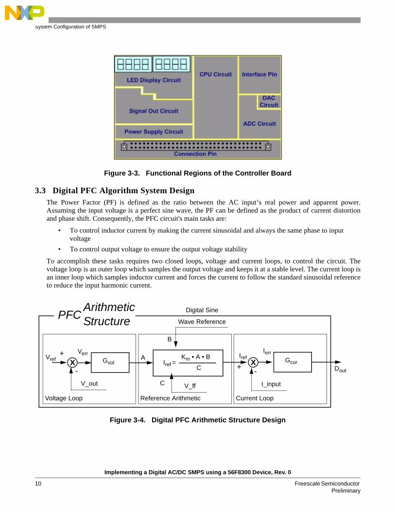
3.3 Digital PFC Algorithm System DesignThe Power Factor (PF) is defined as the ratio between the AC input’s real power and apparent power.Assuming the input voltage is a perfect sine wave, the PF can be defined as the product of current distortion and phase shift. Consequently, the PFC circuit's main tasks are:
• To control inductor current by making the current sinusoidal and always the same phase to input voltage
• To control output voltage to ensure the output voltage stability
To accomplish these tasks requires two closed loops, voltage and current loops, to control the circuit. The voltage loop is an outer loop which samples the output voltage and keeps it at a stable level. The current loop is an inner loop which samples inductor current and forces the current to follow the standard sinusoidal reference to reduce the input harmonic current.
Figure 3-4. Digital PFC Arithmetic Structure Design
XVref
+
-
VerrGvol
V_out
Voltage Loop Reference Arithmetic Current Loop
Digital Sine
Wave Reference
A
B
Iref = Km • A • B
C
V_ff
X Gcur
IerrIref
+ -I_input
Dout
C
Arithmetic StructurePFC

Digital PFC Algorithm System Design
Implementing a Digital AC/DC SMPS using a 56F8300 Device, Rev. 0
Freescale Semiconductor 11 Preliminary
According to PFC theory, PFC arithmetic can be divided into three parts:
• Voltage outer loop, which ensures that the output voltage follows the reference - constant voltage output
• Reference arithmetic, which ensures that the current reference follows the sine reference and constant power feed forward
• Current inner loop, which ensures that the input current follows the given current reference
These items implement the PFC function.
3.3.1 Arithmetic of Current Reference In analog domain control arithmetic, the current reference wave is referred to the input voltage; at the same time, the reciprocal squared input voltage is introduced to maintain the constant power control. The formula is shown in Equation 3-1.
(EQ. 3-1.)
Where:
Km is the proportion value vvo is the output of voltage regulator Vs is the instantaneous value of input voltage vff is the RMS value of feed forward voltage
In analog domain arithmetic, the input voltage sample must be introduced as the input current's reference to insure that the ripple voltage is introduced to current control at the same time. The effect of PFC will be greatly affected under conditions of extreme input. In addition, because the input voltage acts as the current reference, the denominator of current reference will be the square of the input voltage. This adds processing complexityand consequently affects system performance. In a digital control system, the sine reference can be given accurately and conveniently by DSP software, which will not only be a perfect sine wave, so there is no effect from input voltage, but also simplifies the arithmetic structure.
(EQ. 3-2.)
Where:
Ishape is the reference sine wave generated by DSP software Km is proportional value Vvo is the output of voltage regulator Vff is the RMS value of the feed forward voltage
These equations all the conclusion that the current reference is constructed in part from the input voltage in analog arithmetic, which will introduce a ripple voltage to the current control. Therefore, when the operating conditions change, the effects on the PFC will be apparent. Digital arithmetic completely avoids influence from input voltage. The sine reference is generated by DSP software and the wave can be perfect even if the input voltage has great distortion, so the system input current can be a very clean sine wave, which
tVV
vKi s
ff
vomL 02* sinϖ
⋅=
shapeff
vomL I
VVKi ⋅
=*

System Configuration of SMPS
Implementing a Digital AC/DC SMPS using a 56F8300 Device, Rev. 0
12 Freescale Semiconductor Preliminary
consequently results in a perfect PFC effect. In addition, in analog arithmetic, the denominator of current reference must be the square of input voltage to calculate the current reference. The digital equation doesn’t require the square of the input voltage, so it is also simpler.
3.3.2 Design of Voltage and Current LoopsBecause of its simplicity and reliability, PI loop control is a widely used industrial control technique. In this paper, the two control loops adopt PI regulator arithmetic.
The discrete voltage loop structure is shown in Figure 3-5.
Kvs is the output voltage sample modulus GVEA(Z) is the discrete control transfer function Gvh(Z) is the discrete power transfer function.
After deriving the discrete power transfer function, it's necessary to consider the discrete control transfer function.
Figure 3-5. Discrete Voltage Loop Structure
The voltage regulator is based upon the PI regulator, so:
(EQ. 3-3.)
Where:
Kpv is P parameter Kiv is I parameter Kp and ξ are temporary variables
(EQ. 3-4.)
So the voltage open loop transfer function is:
(EQ. 3-5.)
Vo* X GVEA(Z) Gvh(Z)
Kvs
Vo
_
11)(
1)(
−−
=−
−+=
−+=
zzK
zKzKK
zzK
KzG ppvivpviv
pvVEAξ
ivpvp KKK += ,ivpv
pv
KKK
+=ξ
)()()( zGzGKzG vhVEAvsvopen =

DC/DC Converter System Design
Implementing a Digital AC/DC SMPS using a 56F8300 Device, Rev. 0
Freescale Semiconductor 13 Preliminary
To restrain the effect on the current loop caused by second order harmonics in the output voltage, the voltage loop must be able to restrain the harmonics voltage to a range between 100 to 120Hz. So the close frequency is set to 6Hz and the phase margin to 45. According to the characteristics of the open loop transfer function, it’s possible to get the PI parameters of the voltage loop. The current loop also uses a PI regulator with a design similar to the voltage loop's.
3.4 DC/DC Converter System DesignIgnoring the dead time that is inserted by the PWM peripheral, the two switches in one power bridge operate at a 180o complement to each other. Constant output is achieved by adjusting the value of phase shift. When α = 0o, Q1/Q4 or Q2/Q3 are on simultaneously and the output value is at its maximum. When α = 180o, Q1/Q2 or Q3/Q4 are on simultaneously and the output voltage is zero. The 56F8323 samples three signals: output voltage (Vo), primary inductor current (iL), and output current (io).
3.4.1 DC/DC Converter ArithmeticA voltage loop and current loop are used in the system. The error signal is generated by the comparison between the reference and the sample value of the output voltage. The voltage loop is composed of a PI regulator; its input is the error signal. The output of voltage acts as the reference for the current loop and the error signal between the primary inductor current; its reference is the input of the current loop's PI regulator. The current loop outputs the results of its PI regulator, which is the control signal for the phase shift α.
Figure 3-6. Digitally Controlled PSFB Converter
Table 3-1. PFC System PI Parameters
Loop Parameter Symbol Value
Voltage LoopProportion modulus Kpv 5
Integration modulus Kiv 0.007
Current LoopProportion modulus Kpi 0.17
Integration modulus Kii 0.044
XVref
+
-
VerrGvol
V_out
Voltage Loop Current Loop
X Gcur
IerrIref
+ -I_L
Dout
Arithmetic StructurePSFB
PWMGeneration
PWMOutput

System Configuration of SMPS
Implementing a Digital AC/DC SMPS using a 56F8300 Device, Rev. 0
14 Freescale Semiconductor Preliminary
3.4.2 Voltage and Current Loops Design
Figure 3-7. DC/DC Loop Control Structure
PI regulators are also used in the voltage loop and current loop of the PSFB DC/DC converter. The 56F8323-based control is a discrete digital control system;because control results can be calculated according to the sampled value, the transfer function of PI regulator can be shown as in Equation 3-6:
(EQ. 3-6.)
Us is calculated as shown in Equation 3-7.
(EQ. 3-7.)
U(n) is the calculation result corresponding to the nth sample value E(n) is the variable error at the nth sampling time I(n) and I(n-1) are the sum of n sample values and n-1 sample values, respectively K0 is the proportion modulus K1 is the integral modulus Kcorr is the modulus used to prevent saturation Epi prevents saturation Kcorr × Epi operates only when U(n) overflows, so Epi = 0 is typical
The parameters of the voltage and current loops are confirmed by emulation and experiment. To ensure optimum system performance in a wide input voltage, different parameters are adopted when the input voltage is 110V and 220V. This is possible only in a digital system and is impossible when using analog control.
Vo* X GVEA(Z) Gvh(Z)
Kvs
Vo
_
⎪⎩
⎪⎨
⎧
−=×+×+−=
−+×=
)()(1)1()()1()(0)(
nUUsEpiEpiKcorrnEKnInI
nInEKnU
max max
min min
( )( )
( )
U U n UUs U U n U
U n else
≥⎧⎪= ≤⎨⎪⎩

PFC Controller Software Configuration
Implementing a Digital AC/DC SMPS using a 56F8300 Device, Rev. 0
Freescale Semiconductor 15 Preliminary
3.5 PFC Controller Software ConfigurationIn the 56F8323-based PFC module system, the digital controller uses the ADC peripheral to sample the input voltage (Vi), the input current (Iin), and the output voltage (Vbus)from the full-wave rectifier . After the two loops' arithmetic calculation, the 56F8323 software uses the PWM peripheral to send out all driver signals forthe PFC main power circuit. The cap signal of input voltage crossing is sent to the controller for the PFC current phase standard. The device manages the protectioni function, input relay control, the LED display function, and serial SCI communication with the PC and with the secondary-side controller.
Figure 3-8. PFC Control Software Structure
Table 3-2. DC/DC System PI Parameters
Loop Parameter Symbol Value
Voltage Loop
Proportion modulus
Kpv 0.195
Integration modulus
Kiv 0.004
Current Loop
Proportion modulus
Kpi 0.42
Integration modulus
Kii 0.001
Input Voltage Sample
Inductor Current Sample
Output Voltage Sample
HardwareProtection
Secondary DSC
PC
56F8323CAP Input
Voltage Crossing
Driver LED StateDisplay
AD input
CAPinput
SCI0
SCI1
output

System Configuration of SMPS
Implementing a Digital AC/DC SMPS using a 56F8300 Device, Rev. 0
16 Freescale Semiconductor Preliminary
The primary-side 56F8323-based PFC control main program functions include:
• Initialization of program• Interrupt for the voltage loop• Interrupt for the current loop
The system software structure is shown in Figure 3-8. The main program initializes the ADC, PWM, and Timer peripherals, then waits for the generation of interrupts to perform the control loops. Calculating the voltage loop is performed with the voltage interrupt. The current loop is calculated with the current interrupt, according to the current reference. If a fault interrupt occurs, there is a malfunction, and the controller hardware automatically masks all PWM output to protect the PFC hardware. Software in the interrupt service routine takes further action.
3.6 DC/DC Controller Software ConfigurationIn the 56F8323-based DC/DC module system, the digital controller uses the internal ADC peripheral to samplethe output current signal, the resonant inductor current, and the output voltage. After the two loops' arithmetic calculation, the controller software uses the PWM peripheral to send out the driver signals for the DC/DC main power circuit. The PWM uses a fixed-duty drive signal and uses phase shifting techniques to stabilize the output voltage. At the same time, the logic relationship between the synchronous signal and the primary drive signal drives the synchronous converters. Since the control of both is performed in the digital domain using the
Table 3-3. PFC Controller Events
Controller Frequency 60MHz
Instruction Period 16.67ns
PWM Switching Frequency 100kHz
Sampling Rate 100kHz
Analog-to-Digital 1.7µs
Interrupt Name Interrupt Period Interrupt assignment
Voltage Loop 10kHz Timer Calculate the PI of voltage loop;Voltage loop output;Calculate the mean of input voltage
Current loop 100kHz Timer Start ADCCalculate current loop referenceCalculate the PI of current loop and get the new dutyUpdate the PWMProduct ZVS PWM
Fault2 Interrupt Event trigger Power the system off
RS-232 Communication
Interrupt
Event trigger Receive the communication data from secondary-side controllerSet the Switch-on or Protect directive from secondary-side controller

DC/DC Controller Software Configuration
Implementing a Digital AC/DC SMPS using a 56F8300 Device, Rev. 0
Freescale Semiconductor 17 Preliminary
same processor, this is easily and simply implemented. The software of the digital DC/DC converter also includes LED display of output voltage, software protection of output current, and the serial communications with the PC and the primary-side controller.
Figure 3-9. Software Structure of DC/DC Control
The main program of the controller-based DC/DC module includes:
• Initialization of the program• Interrupt for the voltage loop• Interrupt for the current loop
The system’s software structure is shown in Figure 3-9. The main program initializes the ADC, PWM and Timer, then waits for the generation of the control loop interrupts. The interrupt service routine for the voltage loop calculates the voltage loop control algorithm and modifies the PWM setting accordingly. The interrupt service routine for the current loop calculates the current loop according to the current reference. If a fault interrupt occurs, there is a malfunction, and the controller’s hardware automatically masks all PWM output to protect the PFC hardware. Software in the interrupt service routine takes further action.
Output Current Sample
Resonant Inductor Current Sample
Output Voltage Sample
HardwareProtection
Primary DSC56F8323PC
Driver LED StateDisplay
input
output
Operation of Unit and Development Interfaces
Implementing a Digital AC/DC SMPS using a 56F8300 Device, Rev. 0
18 Freescale Semiconductor Preliminary
4. Operation of Unit and Development InterfacesThis section contains a simple overview of how the unit operates. It also describes some of the interfaces that are present to support software development and display the performance of the system, but typically would not be present in a final system.
The operation of the unit is quite simple. When power is applied from a wall socket, the controller is powered on and performs a hardware self-check. After this, the unit power switch will be recognized and if the the POWERON button is down, the controller software starts and the SMPS begins to provide the main output power to the load.
During operation, the LED on the controllers can display the operating parameters of the system. The PFC controller displays the parameter of input voltage and DCBus voltage from left to right in turn. The DC/DC controller displays the parameter of output voltage and output current from left to right in turn. During operation, the SCI port communication provides status data and also accepts control of the unit from the PC.
The design supports the debug function provided by the JTAG interface. For safe mode general debug, the main power can be isolated from the main power circuitry by disconnecting the J14 connector on the power board.
To switch the unit off, press up on the POWERON button; the DSC cuts off the main power, and the bus voltage is decreased. The controller will continue to operate as long as the power cord is plugged in.
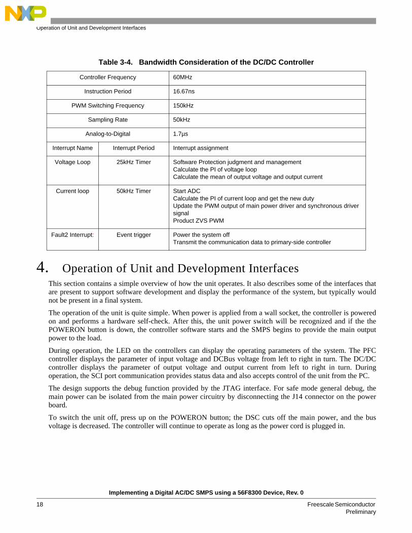
Table 3-4. Bandwidth Consideration of the DC/DC Controller
Controller Frequency 60MHz
Instruction Period 16.67ns
PWM Switching Frequency 150kHz
Sampling Rate 50kHz
Analog-to-Digital 1.7µs
Interrupt Name Interrupt Period Interrupt assignment
Voltage Loop 25kHz Timer Software Protection judgment and managementCalculate the PI of voltage loopCalculate the mean of output voltage and output current
Current loop 50kHz Timer Start ADCCalculate the PI of current loop and get the new dutyUpdate the PWM output of main power driver and synchronous driver signalProduct ZVS PWM
Fault2 Interrupt: Event trigger Power the system offTransmit the communication data to primary-side controller

JTAG Function
Implementing a Digital AC/DC SMPS using a 56F8300 Device, Rev. 0
Freescale Semiconductor 19 Preliminary
Exercise caution with this application:
1. Do not turn on the unit with the power button until the controller board has completely booted up
2. Do not unplug the unit until the unit is completely turned off
3. Major intrusive software debugging should be performed with the power connector J14 disconnected.Real-time debugging using the real-time tools can be performed with J14 in place, as long as the processor is not halted at critical times.
4.1 JTAG Debug Port and SCI Port ConnectionsThe JTAG port interface supports powerful debug and software development functions when used in conjunction with the CodeWarrior IDE. The demonstration contains a Communication Board, which provides mixed communication functions, such as JTAG debug and SCI interface, between the power module and the PC. These interfaces provide electrical isolation between the high-voltage power electronics and the low-voltage development equipment.
The communication system consists of two parts:
• JTAG, which is designed for software debugging and programming• SCI circuits, which are designed for background communication from and to the PC, supporting
real-time debug and control via the software tools
Figure 4-1. Communication Board Block Diagram
4.2 JTAG FunctionBecause the 56800/E core integrates the JTAG/EOnCE function, the 56F8323 can be debugged and programmed by a simple interface circuit through the parallel port without any special emulator. To insure safety, all communication signals between the controller and PC are isolated by optocouplers.

Operation of Unit and Development Interfaces
Implementing a Digital AC/DC SMPS using a 56F8300 Device, Rev. 0
20 Freescale Semiconductor Preliminary
Figure 4-2. JTAG Interface Connection
The connection diagram is shown in Figure 4-2. The JTAG flat cable accessory is connected from the controller board’s J2 connector to the Communication Interface Board’s J204 connector. The JTAG port is connected to the computer by a parallel cable, which links the Communication Interface Board’s J203 to the PC computer parallel port.
Intrusive debugging or downloading a new control program is best processed when the main power is disconnected to the power switches, by disconnecting power connector J14 on the motherboard.
Use caution when debugging the control program with the J14 connector installed, as the device is controlling power circuitry which can be damaged. Controller software debugging should only be performed by anindividual familiar with high-voltage power circuitry and control.
The CodeWarrior for Freescale 56800/E Controllers IDE tool is used to develop the application; Version 6.1 or greater is recommended. Figure 4-3 shows the software interface. See Section 6. for information on the CodeWarrior IDE.
56F8323 Controller Board
JTAG FlatCable
To computerparallel port
Parallel Cable
To J203 ofCommunicationInterface Board
To J204 ofCommunicationInterface Board
To J2 ofController Board
Communications InterfaceBoard

SCI Communication Function
Implementing a Digital AC/DC SMPS using a 56F8300 Device, Rev. 0
Freescale Semiconductor 21 Preliminary
Figure 4-3. CodeWarrior Development Tool GUI interface
4.3 SCI Communication FunctionThis circuit is the serial communication interface between the 56F8323 and the PC. A charge pump voltage converter is used to generate +5V power from the PC, which is the power supply for the RS-232 communication protocol transformer IC.
Figure 4-4. SCI Communication Connection Diagram
56F8323 Controller Board
SCI Flat Cable
Serial Cable
To Computer’sSerial Port
To J201 ofCommunicationInterface Board
To J 3 ofController Board
Communications InterfaceBoard
To J202 ofCommunicationInterface Board

Operation of Unit and Development Interfaces
Implementing a Digital AC/DC SMPS using a 56F8300 Device, Rev. 0
22 Freescale Semiconductor Preliminary
The SCI communication connection diagram is shown in Figure 4-4. The SCI flat cable accessory is connected from the 56F8323 controller board’s J3 to the Communication Interface Board. The Controller Board’s J3 PIN1 must be linked to the Communication Interface Board’s J201 PIN1. At the same time, the serial cable links the Communication Interface Board’s J202 and the PC’s serial port.
The PC master software for real-time debugging and control is included with the CodeWarrior software installation. The PC master software uses the SCI port as the communication channel. The PC master software reads data from the 56F8323 target and can graphically display this data. This reference design includes a PCmaster software project that displays target data using the PC master software digital oscilloscope graphing function and can also be used to control the demonstration. Detailed information on the use and features of the PC master software tool is included in the CodeWarrior installation.
To use the PC master software tool with this design, open the project files included in the design. The PFC processor is supported with the project PFCsupervisal.pmp, and the DC/DC processor is supported with the project file DCDCsupervisal.pmp. Figure 4-5 shows the PC master software interface with the digital oscilloscope and variable watch points. The data presented in the oscilloscope and variable watch points are from the 56F8323 processor, which is running in real time.
Figure 4-5. CodeWarrior PC Master Software Tool Interface
The PC master software tool must be configured so that the RS-232 set-up for the computer is the same as the SCI set-up on the 56F8323. This option is set in the item Project -> Option. In the Option dialog box, the right communication port on the PC and SCI configuration parameters as follows:
Baud rate: 9600 baudParity: NoneWidth: 8 bitsStop bit: 1 bitBreak signal: DisableHandshake of CTS & RTS: Disable

SCI Communication Function
Implementing a Digital AC/DC SMPS using a 56F8300 Device, Rev. 0
Freescale Semiconductor 23 Preliminary
5. ConclusionThis reference design implements a complete high-performance digital AC/DC SMPS. As shown, using full digital control, the SMPS systems become flexible and can also realize complex control arithmetic which is difficult or impossible for analog control to perform. A digital signal controller-based SMPS system integrateshigh-performance digital signal processing with power electronics, providing new methods for design of power electronics, and providing the typical high-level control and communication capability required in an SMPS system. This reference design uses the Freescale 56F8323 to perform the input power factor correction and phase-shifted full-bridge DC/DC power conversion with excellent efficiency, low cost, and design flexibility.
For more information, the Design Reference Manual includes detailed hardware and software information, schematics and a bill of material; see Section 6.
In conjunction with our high-performance 56F8300 products and advanced hardware and software tools, you can create a complete system solution, easily including your own value-added intellectual property.
6. References1. 56F8300 Peripheral User Manual,MC56F8300UM, Freescale Semiconductor, Inc.
2. 56F8323/56F8123 Data Sheet, MC56F8323, Freescale Semiconductor, Inc.
3. Design of the 56F8323 Using SMPS, DRM074, Freescale Semiconductor, Inc.
To provide the most up-to-date information, the revision of our documents on the World Wide Web will be the most current. Your printed copy may be an earlier revision. To verify that you have the latest information available, refer to www.freescale.com or contact your Freescale representative.

How to Reach Us:
Home Page:www.freescale.com
E-mail:[email protected]
USA/Europe or Locations Not Listed:Freescale SemiconductorTechnical Information Center, CH3701300 N. Alma School Road Chandler, Arizona 85224 +1-800-521-6274 or [email protected]
Europe, Middle East, and Africa:Freescale Halbleiter Deutschland GmbHTechnical Information CenterSchatzbogen 781829 Muenchen, Germany+44 1296 380 456 (English)+46 8 52200080 (English)+49 89 92103 559 (German)+33 1 69 35 48 48 (French)[email protected]
Japan:Freescale Semiconductor Japan Ltd. HeadquartersARCO Tower 15F1-8-1, Shimo-Meguro, Meguro-ku,Tokyo 153-0064, Japan0120 191014 or +81 3 5437 [email protected]
Asia/Pacific:Freescale Semiconductor Hong Kong Ltd.Technical Information Center 2 Dai King Street Tai Po Industrial Estate Tai Po, N.T., Hong Kong +800 2666 [email protected]
For Literature Requests Only:Freescale Semiconductor Literature Distribution CenterP.O. Box 5405Denver, Colorado 802171-800-441-2447 or 303-675-2140Fax: [email protected]
Freescale™ and the Freescale logo are trademarks of Freescale Semiconductor, Inc. All other product or service names are the property of their respective owners. This product incorporates SuperFlash® technology licensed from SST.© Freescale Semiconductor, Inc. 2005. All rights reserved.
AN3115Rev. 008/2005
Information in this document is provided solely to enable system and software implementers to use Freescale Semiconductor products. There are no express or implied copyright licenses granted hereunder to design or fabricate any integrated circuits or integrated circuits based on the information in this document.
Freescale Semiconductor reserves the right to make changes without further notice to any products herein. Freescale Semiconductor makes no warranty, representation or guarantee regarding the suitability of its products for any particular purpose, nor does Freescale Semiconductor assume any liability arising out of the application or use of any product or circuit, and specifically disclaims any and all liability, including without limitation consequential or incidental damages. “Typical” parameters that may be provided in Freescale Semiconductor data sheets and/or specifications can and do vary in different applications and actual performance may vary over time. All operating parameters, including “Typicals”, must be validated for each customer application by customer’s technical experts. Freescale Semiconductor does not convey any license under its patent rights nor the rights of others. Freescale Semiconductor products are not designed, intended, or authorized for use as components in systems intended for surgical implant into the body, or other applications intended to support or sustain life, or for any other application in which the failure of the Freescale Semiconductor product could create a situation where personal injury or death may occur. Should Buyer purchase or use Freescale Semiconductor products for any such unintended or unauthorized application, Buyer shall indemnify and hold Freescale Semiconductor and its officers, employees, subsidiaries, affiliates, and distributors harmless against all claims, costs, damages, and expenses, and reasonable attorney fees arising out of, directly or indirectly, any claim of personal injury or death associated with such unintended or unauthorized use, even if such claim alleges that Freescale Semiconductor was negligent regarding the design or manufacture of the part.