Embed Size (px)
Citation preview

© Freescale Semiconductor, Inc., 2011. All rights reserved.
Freescale SemiconductorApplication Note
AN4289Rev. 2.0, 3/2011
1 OverviewBasic functionality for Freescale’s family of LIN alternator regulators is provided along with a detailed description for practical applications. Parameters are available by fuse providing product alignment with your application profile.
2 IntroductionThe LIN alternator regulator family of devices is specially designed to work in adverse environments. It supplies a current through a high side MOSFET to the excitation coil of the alternator and provides an internal freewheeling diode. It’s main functionality is to keep the battery at its nominal value, whatever the vehicle demand. The protection and diagnosis may be programmed using OTP (non-volatile Memory).
Additionally, these devices have a fail-safe mode for continuous battery charging in the event LIN is disconnected.
LIN Alternator Regulator Devices
Contents1 Overview . . . . . . . . . . . . . . . . . . . . . . . . . . . . . 12 Introduction. . . . . . . . . . . . . . . . . . . . . . . . . . . 1
2.1 Protection and Diagnostics . . . . . . . . . . . 22.2 Operational Modes . . . . . . . . . . . . . . . . . . 2
3 Fuse Options. . . . . . . . . . . . . . . . . . . . . . . . . . 34 LIN Protocol. . . . . . . . . . . . . . . . . . . . . . . . . . . 8
4.1 Message Frame . . . . . . . . . . . . . . . . . . . . . 84.2 Bit Rate . . . . . . . . . . . . . . . . . . . . . . . . . . . 9
5 Operational Mode Examples . . . . . . . . . . . . 106 Packaging . . . . . . . . . . . . . . . . . . . . . . . . . . . 12
6.1 Die Dimensions . . . . . . . . . . . . . . . . . . . . 126.2 Die Characteristics . . . . . . . . . . . . . . . . . 136.3 Assembly Recommendations . . . . . . . . 13
LIN Alternator Regulator Devices, Rev. 2.02 Freescale Semiconductor
Introduction
2.1 Protection and DiagnosticsThese devices incorporate the following protections and diagnostics, some of which are programmable and can be reported using LIN (version 1.3) to the Engine Control Unit (ECU). For more information please refer the device’s data sheet. (www.freescale.com)
• Thermal protection• Thermal compensation• Over-current detection (LIN and EXC)• Over-voltage• Resistive short-circuit detection (excitation to ground)• High phase level missing• LIN protocol errors (checksum, slave not responding, sync break error, parity)• LIN bus time-out
2.2 Operational ModesThe LIN alternator regulator family has four operating modes: Standby mode (car parking), Pre-excitation mode (with LIN and no phase activity), Default mode (without LIN communication and with phases) and Normal mode.
These devices change its current consumption and capabilities depending on the operational mode. Detailed information for each of the modes can be found in the device’s data sheet.
LIN Alternator Regulator Devices, Rev. 2.0Freescale Semiconductor 3
Fuse Options
3 Fuse Options
3.1 Self-Start Option (Active / Not Active)NOTE
If the LIN communication recovers during self-start operation, the LIN immediately takes the priority and new parameters coming from the Master (ID #29) will be considered.
Self-start option allows the product to start the regulation whereas there is no LIN communication between the master and the slave (LIN wire disconnection or ECU not functional). In that case the product takes internal default parameters programed at Freescale production line as new reference and apply them as soon as the phase frequency reaches the self-start threshold.
3.2 Self-start Threshold (3000 / 4000 RPM)Two selectable values are available in the product indicating at which rotation speed the device will start the regulation. Those values are the same whatever the number of poles of the alternator. This is present only when the self-start option has been activated by the fuse.
The signal used for speed measurement are coming from stator windings (Phase1 and Phase2). For more information, please refer to the application diagram in the device data sheet.
3.3 Phase Sensitivity (0.45 V / 0.9 V / 1.35 V / 1.8 V)Phase sensitivity is linked to the phase signal voltage level coming from the stator windings. Phase signals are naturally out of phase by 120°. The device measures, in real time, the delta voltage between Phase 1 and Phase 2.
As soon as the voltage level difference between Phase 1 and Phase 2 reaches the desired phase sensitivity level AND if phase frequency is high enough (fstart), the product will start regulation.
3.4 Default Regulation Voltage (From 13.5 V to 15 V with 100m V Steps)
The default regulation voltage is used only if the LIN communication between the master and slave (LIN wire disconnection or ECU not functional) is lost during operation. In that case, the target regulation voltage becomes the one programmed in the default regulation voltage (in normal operation). The target regulation voltage is the one present in LIN MID#29 coming from the master.
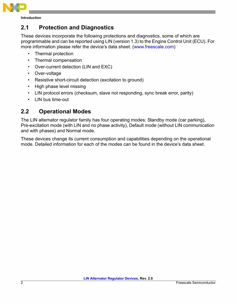
Table 1. Version Determined Electrical Parameters
Self-StartSelf-start Threshold
(RPM)
Phase sensitivity
(V)
Default regulation voltage (V)
Fstart (RPM)
Fstop(RPM)
LRCRates
LRC disable (RPM)
Crest Regulation
BUS inactivity
Thermal Fault
Threshold
thermal compensation threshold (°C)
Special LIN Feature
Alternator Pole-Pair
Slave Address
Active/Not Active
3000 / 4000 0.45/0.9/1.35/1.8
13.5 to 15 (100 mV steps)
800/1050/1300/1550/1800/2050/23
00/2500
500/650/850/1000
0/3/6.4/12.3
2400/3000/4000/never
Active / Not Active
1.3/3 135/145/150/160
135/145/150/160
Active/Not active
6/8 A/B

LIN Alternator Regulator Devices, Rev. 2.04 Freescale Semiconductor
Fuse Options
3.5 Fstart (800, 1050, 1300, 1550, 1800, 2050, 2300, 2500 RPM)Engine speed is reflected on the phase signals. The phase frequency depends on both engine speed and the number of poles in the alternator. The regulator uses this information to start the regulation voltage.
This Fstart value is used only if LIN communication is valid otherwise the self-start speed threshold is considered.
3.6 Fstop (500, 650, 850, 1000 RPM)This parameter indicates to the regulator at which alternator rotation speed it must stop the battery regulation function. This value corresponds usual to vehicle stops.
3.7 LRC Rate (0, 3, 6.4, 12.3s)Load Response Control (LRC) function is very useful when there is a high vehicle load demand combined with a low engine speed. The LRC function controls the rotor current increase at the specified rate up to the LRC disable frequency. This function is only active for duty cycle increases: if there is a load unballasting, the excitation duty cycle is instantly reduced to the duty cycle corresponding to the new battery charge state. The alternator responds to loads commutation in the vehicle, slowly increasing the current in the rotor (EXC duty cycle). The LRC is mainly present at idle speed to avoid stalling the car.
3.8 LRC Disable (2400, 3000, 4000, Never RPM)This specifies the rotation speed the LRC function is disabled. Above this rotation speed the changes in the duty cycle will be instantly done.
3.9 BUS inactivity (1.3, 3 s)The regulator is checking continuously the activity on the BUS. If there is no LIN activity during the specified period, the regulator takes the following actions:
• If there is phase activity coming from stator, the regulator loads the internal default parameter and acts accordingly
• If there is no phase activity, the regulator goes back in Standby mode.
3.10 Default LIN Readout (T°, Current)The regulator, under the MID#11 LIN command from master, can send back to the ECU junction temperature (Tj) OR rotor current (not both). The choice must be specified through this option and programmed at Freescale.
LIN Alternator Regulator Devices, Rev. 2.0Freescale Semiconductor 5
Fuse Options
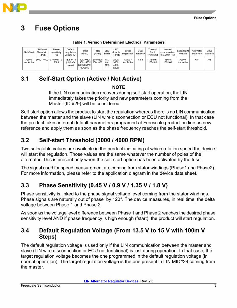
Figure 1. Temperature or Current Data Location in MID#11
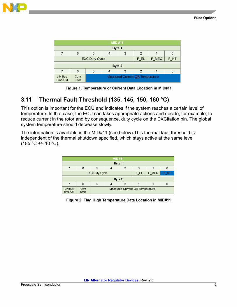
3.11 Thermal Fault Threshold (135, 145, 150, 160 °C)This option is important for the ECU and indicates if the system reaches a certain level of temperature. In that case, the ECU can takes appropriate actions and decide, for example, to reduce current in the rotor and by consequence, duty cycle on the EXCitation pin. The global system temperature should decrease slowly.
The information is available in the MID#11 (see below).This thermal fault threshold is independent of the thermal shutdown specified, which stays active at the same level (185 °C +/- 10 °C).
Figure 2. Flag High Temperature Data Location in MID#11
MID #11Byte 1
7 6 5 4 3 2 1 0EXC Duty Cycle F_EL F_MEC F_HT
Byte 27 6 5 4 3 2 1 0
LIN Bus Time-Out
Com Error
Measured Current OR Temperature
MID #11Byte 1
7 6 5 4 3 2 1 0EXC Duty Cycle F_EL F_MEC F_HT
Byte 27 6 5 4 3 2 1 0
LIN Bus Time-Out
Com Error
Measured Current OR Temperature
LIN Alternator Regulator Devices, Rev. 2.06 Freescale Semiconductor
Fuse Options
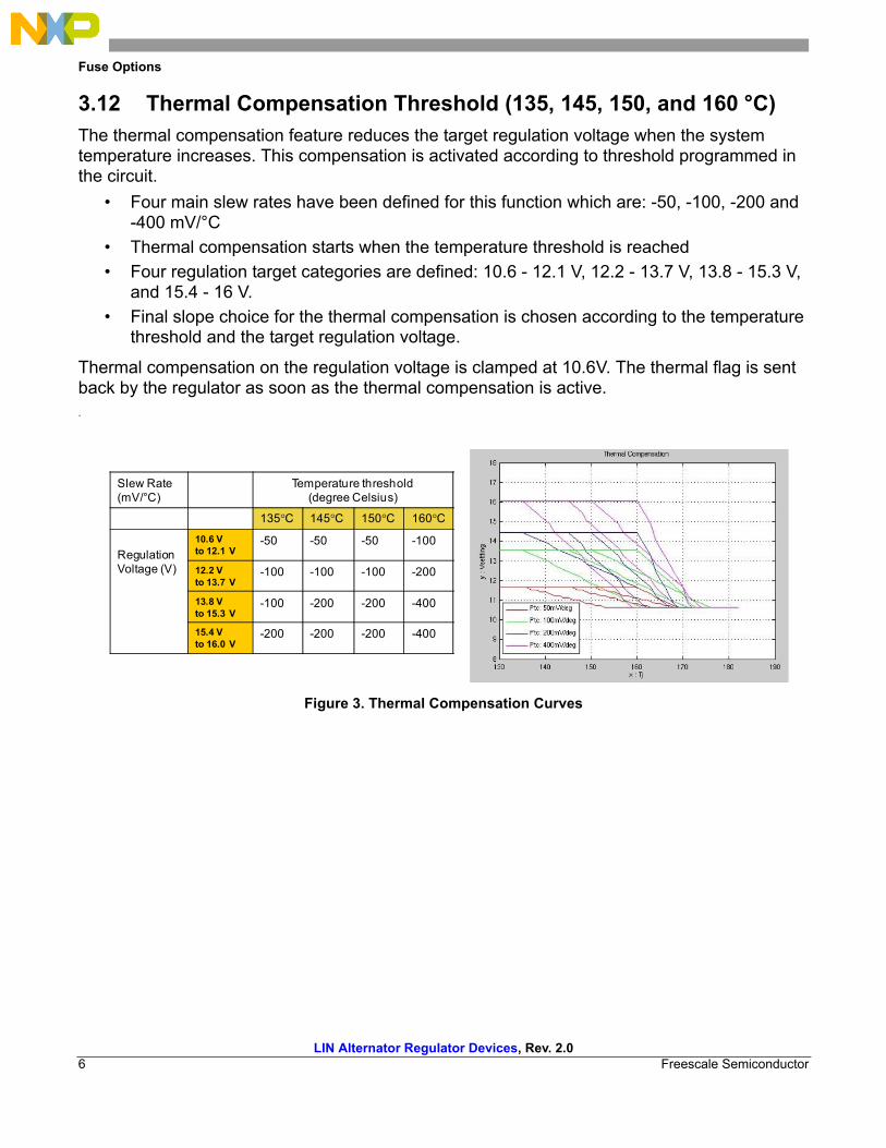
3.12 Thermal Compensation Threshold (135, 145, 150, and 160 °C)The thermal compensation feature reduces the target regulation voltage when the system temperature increases. This compensation is activated according to threshold programmed in the circuit.
• Four main slew rates have been defined for this function which are: -50, -100, -200 and -400 mV/°C
• Thermal compensation starts when the temperature threshold is reached• Four regulation target categories are defined: 10.6 - 12.1 V, 12.2 - 13.7 V, 13.8 - 15.3 V,
and 15.4 - 16 V.• Final slope choice for the thermal compensation is chosen according to the temperature
threshold and the target regulation voltage.
Thermal compensation on the regulation voltage is clamped at 10.6V. The thermal flag is sent back by the regulator as soon as the thermal compensation is active..
Figure 3. Thermal Compensation Curves
Slew Rate (mV/°C)
Temperature threshold (degree Celsius)
135°C 145°C 150°C 160°C
RegulationVoltage (V)
10.6 Vto 12.1 V
-50 -50 -50 -100
12.2 Vto 13.7 V
-100 -100 -100 -200
13.8 Vto 15.3 V
-100 -200 -200 -400
15.4 Vto 16.0 V
-200 -200 -200 -400

LIN Alternator Regulator Devices, Rev. 2.0Freescale Semiconductor 7
Fuse Options
3.13 Special LIN feature (Active / Not Active)This function, when activated by fuse, allows the master (ECU) to command the regulator to not charge the rotor (no current) whatever the conditions are in the vehicle (load, speed, battery charge level). Sending a 10.6 V target regulation voltage in MID#29, enables this feature. If another target regulation voltage is asked by the ECU, the product will regulate the battery at the required voltage then, if a new 10.6 V command is sent, the EXC will be switched off.
It is important to note that if this command is programmed not active, the 10.6 V command (EXC=0) is available only one-time after a cranking and if the ECU did not change the target regulation from 10.6 V to other ones (up to 16 V). Once the product started a regulation cycle, the 10.6 V command is then no more available and 10.6 V becomes a target regulation voltage like others.
Figure 4. Target Regulation Voltage Data Location in MID#29
3.14 Alternator Pole Pair (6, 7, 8, 9 Poles)Depending on the machine type, and to adapt the frequency conversion on the phase signal compared to real RPM, the alternator pole pair number must be programmed.
3.15 Crest Regulation (Active, Not Active)Crest regulation fuse not active: in the case of a load dump, EXC is stopped when the internal filter reaches the load dump detection threshold (~21 V typ.). The delay is given by the internal filter (~1.0 ms).
Crest regulation fuse active: in the case of a load dump, EXC is stopped immediately when the internal ADC reaches 21 V typical. The delay is given by the ADC conversion (~16 µs).
MID #29Byte 1
7 6 5 4 3 2 1 0X X Target Regulation Voltage
Byte 27 6 5 4 3 2 1 0
Ramp Cutoff Ramp Rate
Byte 3
7 6 5 4 3 2 1 0
X X X X Current Limitation
Byte 4
7 6 5 4 3 2 1 0
X X X X X X X X

LIN Alternator Regulator Devices, Rev. 2.08 Freescale Semiconductor
LIN Protocol
4 LIN ProtocolThe version of LIN protocol used in our product is REV 1.3 (available on demand on the Web)
4.1 Message Frame
Figure 5. LIN standard Message Frame
Three identifier field are recognized by the product which are MID#29, MID #11, MID #12.
MID#29 is a writing command (4 bytes) then MID#11 and MID#12 are read commands (2 bytes).
the data in the MID are fixed and must be respected and are organized in the following way.
Figure 6. LIN MID#29 Writing Command
MID #29Byte 1
7 6 5 4 3 2 1 0X X Target Regulation Voltage
Byte 27 6 5 4 3 2 1 0
Ramp Cutoff Ramp Rate
Byte 3
7 6 5 4 3 2 1 0
X X X X Current Limitation
Byte 4
7 6 5 4 3 2 1 0
X X X X X X X X
LIN Alternator Regulator Devices, Rev. 2.0Freescale Semiconductor 9
LIN Protocol
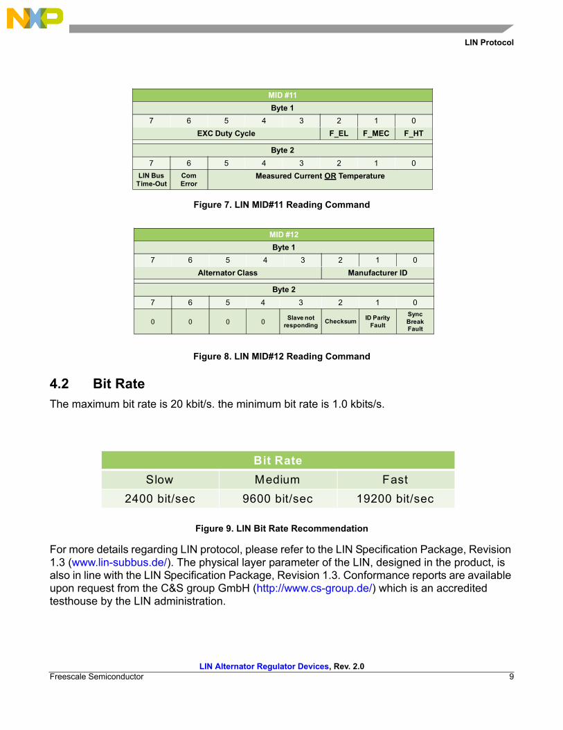
Figure 7. LIN MID#11 Reading Command
Figure 8. LIN MID#12 Reading Command
4.2 Bit RateThe maximum bit rate is 20 kbit/s. the minimum bit rate is 1.0 kbits/s.
Figure 9. LIN Bit Rate Recommendation
For more details regarding LIN protocol, please refer to the LIN Specification Package, Revision 1.3 (www.lin-subbus.de/). The physical layer parameter of the LIN, designed in the product, is also in line with the LIN Specification Package, Revision 1.3. Conformance reports are available upon request from the C&S group GmbH (http://www.cs-group.de/) which is an accredited testhouse by the LIN administration.
MID #11Byte 1
7 6 5 4 3 2 1 0EXC Duty Cycle F_EL F_MEC F_HT
Byte 27 6 5 4 3 2 1 0
LIN Bus Time-Out
Com Error
Measured Current OR Temperature
MID #12Byte 1
7 6 5 4 3 2 1 0Alternator Class Manufacturer ID
Byte 27 6 5 4 3 2 1 0
0 0 0 0 Slave not responding Checksum ID Parity
Fault
Sync Break Fault
Bit RateSlow Medium Fast
2400 bit/sec 9600 bit/sec 19200 bit/sec
LIN Alternator Regulator Devices, Rev. 2.010 Freescale Semiconductor
Operational Mode Examples
5 Operational Mode Examples
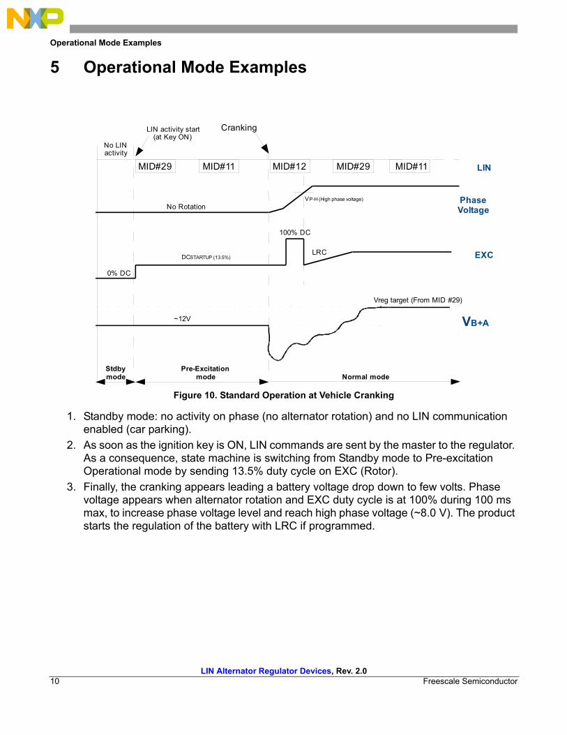
Figure 10. Standard Operation at Vehicle Cranking
1. Standby mode: no activity on phase (no alternator rotation) and no LIN communication enabled (car parking).
2. As soon as the ignition key is ON, LIN commands are sent by the master to the regulator. As a consequence, state machine is switching from Standby mode to Pre-excitation Operational mode by sending 13.5% duty cycle on EXC (Rotor).
3. Finally, the cranking appears leading a battery voltage drop down to few volts. Phase voltage appears when alternator rotation and EXC duty cycle is at 100% during 100 ms max, to increase phase voltage level and reach high phase voltage (~8.0 V). The product starts the regulation of the battery with LRC if programmed.
LIN
PhaseVoltage
EXC
MID#29 MID#11
CrankingLIN activity start(at Key ON)
DCSTARTUP (13.5%)
VB+A~12V
Stdbymode
Pre-Excitationmode
No Rotation
0% DC
No LIN activity
MID#12 MID#29 MID#11
Vreg target (From MID #29)
Normal mode
100% DC
LRC
VP-H (High phase voltage)

LIN Alternator Regulator Devices, Rev. 2.0Freescale Semiconductor 11
Operational Mode Examples
Figure 11. Self-start Operation (No LIN Communication)
1. Standby mode: no activity on phase (no alternator rotation) and no LIN communication enabled (car parking)
2. During cranking, the device detects phase signal, and the device is activated, but don’t see any activity on LIN pin. It is taking as reference all default parameter programmed and is waiting phase frequency for witch it must start the regulation.
3. As soon as the self-start threshold speed is reached (3000 or 4000 RPM), the device starts the battery regulation.
L IN
P h a s eF re q u e n c y
E X C
C ra n k in g
V B + A~ 1 2 V
S td b y m o d e
N o R o t a t io n
0 % D C
N o L I N a c t iv i t y
V re g t a rg e t (p ro g ra m m e d b y d e f a u l t )
D e fa u l t m o d e
0 % D C
S e l f s ta r t T h re s h o ld(3 0 0 0 o r 4 0 0 0 R P M )
S e l f-s ta r tP h a s e a c ti v e
b u t n o L I N c o m
4 0 % D C (e x a m p le )
LIN Alternator Regulator Devices, Rev. 2.012 Freescale Semiconductor
Packaging
6 Packaging
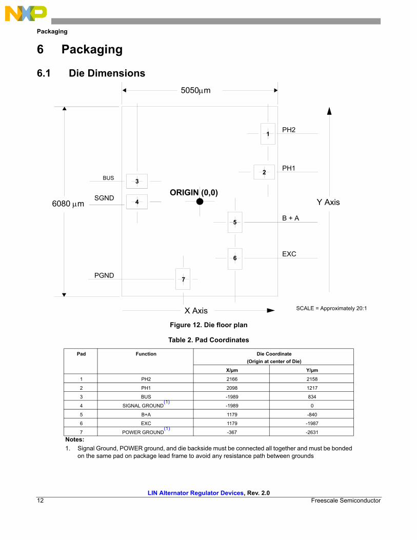
6.1 Die Dimensions
Figure 12. Die floor plan
Table 2. Pad Coordinates
Pad Function Die Coordinate(Origin at center of Die)
X/µm Y/µm
1 PH2 2166 2158
2 PH1 2098 1217
3 BUS -1989 834
4 SIGNAL GROUND(1)
-1989 0
5 B+A 1179 -840
6 EXC 1179 -1987
7 POWER GROUND(1)
-367 -2631Notes: 1. Signal Ground, POWER ground, and die backside must be connected all together and must be bonded
on the same pad on package lead frame to avoid any resistance path between grounds
PH1
6080 μm
PH2
5050μm
Y AxisORIGIN (0,0)
X Axis
1
23
4
5
6
7
B + A
EXC
PGND
SGND
BUS
SCALE = Approximately 20:1

LIN Alternator Regulator Devices, Rev. 2.0Freescale Semiconductor 13
Packaging
6.2 Die CharacteristicsThe die is designed to be fitted into a customer designed package however, as so many wiring configurations exist, not all may be possible from the same die design. Due to thermal considerations, soldering is the preferred die attach method, but under some circumstances, conductive epoxy may be acceptable.
6.3 Assembly RecommendationsValues below are for information only and are based on Freescale experiments. A complete
characterization/validation by the customer is needed to fully qualify the assembly process. Freescale will not be responsible of the customer’s assembly process.
Table 3. Physical Die Characteristics
Mechanical Data Lenght Width UnitsBonding Pad Size 0.66 0.5 mmDie Size (lenght x Width) 6.08 5.05 mmDie Back Metal Composition Cr/CrAg/AgDie Back Metal Thickness, Typical 2.1 µmDie Top Metal Thickness, Typical 2.0 µmDie Top Metal Composition 99.5 Al 0.5Cu %Die Thickness 0.36 mm
Table 4. Mechanical Data
Mechanical Data DescriptionWire Bonding Aluminum, 8 Mils DiameterAssembly Process Type Wedgebond ProcessMaximum End Force to apply 320 Gr(2)
Minimum End Force to apply 180 Gr(3)
Notes: 2. To avoid any mechanical damage to the part, the end force pressure must be controlled ensuring the
assembly process and should not exceed this value.3. Lower value could degrade wire shear performance.
LIN Alternator Regulator Devices, Rev. 2.014 Freescale Semiconductor
Packaging
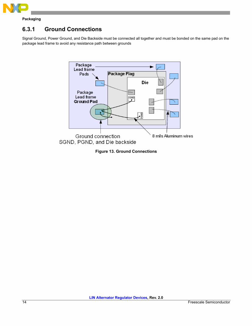
6.3.1 Ground ConnectionsSignal Ground, Power Ground, and Die Backside must be connected all together and must be bonded on the same pad on the package lead frame to avoid any resistance path between grounds
Figure 13. Ground Connections

How to Reach Us:
Home Page:www.freescale.com
Web Support:http://www.freescale.com/support
USA/Europe or Locations Not Listed:Freescale Semiconductor, Inc.Technical Information Center, EL5162100 East Elliot Road Tempe, Arizona 85284 1-800-521-6274 or +1-480-768-2130www.freescale.com/support
Europe, Middle East, and Africa:Freescale Halbleiter Deutschland GmbHTechnical Information CenterSchatzbogen 781829 Muenchen, Germany+44 1296 380 456 (English)+46 8 52200080 (English)+49 89 92103 559 (German)+33 1 69 35 48 48 (French)www.freescale.com/support
Japan:Freescale Semiconductor Japan Ltd. Headquarters ARCO Tower 15F 1-8-1, Shimo-Meguro, Meguro-ku, Tokyo 153-0064 Japan 0120 191014 or +81 3 5437 [email protected]
Asia/Pacific:Freescale Semiconductor China Ltd. Exchange Building 23F No. 118 Jianguo Road Chaoyang District Beijing 100022 China +86 10 5879 [email protected]
For Literature Requests Only:Freescale Semiconductor Literature Distribution CenterP.O. Box 5405Denver, Colorado 802171-800-441-2447 or +1-303-675-2140Fax: [email protected]
Freescale™ and the Freescale logo are trademarks of Freescale Semiconductor, Inc. All other product or service names are the property of their respective owners.© Freescale Semiconductor, Inc., 2011. All rights reserved.
AN4289Rev. 2.05/2011
Information in this document is provided solely to enable system and software implementers to use Freescale Semiconductor products. There are no express or implied copyright licenses granted hereunder to design or fabricate any integrated circuits or integrated circuits based on the information in this document.
Freescale Semiconductor reserves the right to make changes without further notice to any products herein. Freescale Semiconductor makes no warranty, representation or guarantee regarding the suitability of its products for any particular purpose, nor does Freescale Semiconductor assume any liability arising out of the application or use of any product or circuit, and specifically disclaims any and all liability, including without limitation consequential or incidental damages. “Typical” parameters that may be provided in Freescale Semiconductor data sheets and/or specifications can and do vary in different applications and actual performance may vary over time. All operating parameters, including “Typicals”, must be validated for each customer application by customer’s technical experts. Freescale Semiconductor does not convey any license under its patent rights nor the rights of others. Freescale Semiconductor products are not designed, intended, or authorized for use as components in systems intended for surgical implant into the body, or other applications intended to support or sustain life, or for any other application in which the failure of the Freescale Semiconductor product could create a situation where personal injury or death may occur. Should the Buyer purchase or use Freescale Semiconductor products for any such unintended or unauthorized application, the Buyer shall indemnify and hold Freescale Semiconductor and its officers, employees, subsidiaries, affiliates, and distributors harmless against all claims, costs, damages, and expenses, and reasonable attorney fees arising out of, directly or indirectly, any claim of personal injury or death associated with such unintended or unauthorized use, even if such claim alleges that Freescale Semiconductor was negligent regarding the design or manufacture of the part.
RoHS-compliant and/or Pb-free versions of Freescale products have the functionality and electrical characteristics of their non-RoHS-compliant and/or non-Pb-free counterparts. For further information, see http://www.freescale.com or contact your Freescale sales representative.
For information on Freescale’s Environmental Products program, go to http://www.freescale.com/epp.