Embed Size (px)
Citation preview

November 2014 DocID025366 Rev 2 1/25
25
AN4374Application note
The LED1642GW and ALED1642GW start-up guide
Fabio Occhipinti
IntroductionThe use of LEDs in applications like displays, information and advertising panels, signs, traffic signals, automotive lighting and architectural lighting is becoming more and more popular. The LED array drivers, with accurate constant current regulation and embedded serial interface, are the solution suitable for the above mentioned applications. This document provides an overview about the LED1642GW LED array driver and the ALED1642GW (automotive grade version). The first part of this document is focused on the device startup, as well as the main communication key explanation for an easy use of this product. The last part of this document gives some general guidelines relative to the application dimensioning and the PCB design.
Figure 1. LED1642GW and ALED1642GW block diagram
UVLO & POR
Configuration register
Channel driverTiming controlTurn ON/OFFGradual delay
……
……
Current gain adjustment
SDICLKLE
VDD
GND
R-EXT
SDO
OUT0
OUT1
OUT2
OUT14
OUT15
16 output channels
PWM counter
PWCLK
Thermal shutdown
CurrentRef.
Control Logic &Data Registers
Error detection
AM16850v1
www.st.com

Contents AN4374
2/25 DocID025366 Rev 2
Contents
1 The LED1642GW and ALED1642GW basic circuit . . . . . . . . . . . . . . . . . 4
2 First LED power-on . . . . . . . . . . . . . . . . . . . . . . . . . . . . . . . . . . . . . . . . . . 4
3 LED power-on at maximum current and 50% duty cycle . . . . . . . . . . . 9
4 The PWCLK frequency choice . . . . . . . . . . . . . . . . . . . . . . . . . . . . . . . . 12
5 Output error detection . . . . . . . . . . . . . . . . . . . . . . . . . . . . . . . . . . . . . . 13
6 LED supply voltage . . . . . . . . . . . . . . . . . . . . . . . . . . . . . . . . . . . . . . . . . 19
7 Higher current requests (outputs in parallel) . . . . . . . . . . . . . . . . . . . . 21
8 PCB layout guidelines . . . . . . . . . . . . . . . . . . . . . . . . . . . . . . . . . . . . . . 21
9 Revision history . . . . . . . . . . . . . . . . . . . . . . . . . . . . . . . . . . . . . . . . . . . 24

DocID025366 Rev 2 3/25
AN4374 List of figures
25
List of figures
Figure 1. LED1642GW and ALED1642GW block diagram . . . . . . . . . . . . . . . . . . . . . . . . . . . . . . . . . 1Figure 2. LED1642GW and ALED1642GW typical application circuit . . . . . . . . . . . . . . . . . . . . . . . . . 4Figure 3. Digital key summary chart-data latch . . . . . . . . . . . . . . . . . . . . . . . . . . . . . . . . . . . . . . . . . . 5Figure 4. Brightness register setting . . . . . . . . . . . . . . . . . . . . . . . . . . . . . . . . . . . . . . . . . . . . . . . . . . 6Figure 5. Brightness register: first BRT word example. . . . . . . . . . . . . . . . . . . . . . . . . . . . . . . . . . . . . 6Figure 6. Brightness register: last BRT word example. . . . . . . . . . . . . . . . . . . . . . . . . . . . . . . . . . . . . 7Figure 7. Digital key summary chart-write switch. . . . . . . . . . . . . . . . . . . . . . . . . . . . . . . . . . . . . . . . . 8Figure 8. Switch register, example 1 . . . . . . . . . . . . . . . . . . . . . . . . . . . . . . . . . . . . . . . . . . . . . . . . . . 8Figure 9. Channel data and write switch . . . . . . . . . . . . . . . . . . . . . . . . . . . . . . . . . . . . . . . . . . . . . . 10Figure 10. LED1642GW and ALED1642GW configuration register . . . . . . . . . . . . . . . . . . . . . . . . . . 10Figure 11. LED1642GW and ALED1642GW brightness register: first word example . . . . . . . . . . . . . 11Figure 12. LED1642GW and ALED1642GW brightness register: last word example . . . . . . . . . . . . . 11Figure 13. PWCLK counter and comparator . . . . . . . . . . . . . . . . . . . . . . . . . . . . . . . . . . . . . . . . . . . . 12Figure 14. Normal detection sequence . . . . . . . . . . . . . . . . . . . . . . . . . . . . . . . . . . . . . . . . . . . . . . . . 13Figure 15. Digital key summary chart-detection. . . . . . . . . . . . . . . . . . . . . . . . . . . . . . . . . . . . . . . . . . 14Figure 16. Error detection power-on timing . . . . . . . . . . . . . . . . . . . . . . . . . . . . . . . . . . . . . . . . . . . . . 15Figure 17. LED1642GW and ALED1642GW error detection: open detection start . . . . . . . . . . . . . . . 15Figure 18. LED1642GW and ALED1642GW error detection: short detection start . . . . . . . . . . . . . . . 16Figure 19. LED1642GW and ALED1642GW error detection: combined detection start . . . . . . . . . . . 17Figure 20. LED1642GW and ALED1642GW error detection: detection end . . . . . . . . . . . . . . . . . . . . 17Figure 21. Interface signal filtering. . . . . . . . . . . . . . . . . . . . . . . . . . . . . . . . . . . . . . . . . . . . . . . . . . . . 22

The LED1642GW and ALED1642GW basic circuit AN4374
4/25 DocID025366 Rev 2
1 The LED1642GW and ALED1642GW basic circuit
The below figure shows the LED1642GW and ALED1642GW basic application schematic:
Figure 2. LED1642GW and ALED1642GW typical application circuit
we can use Cin =1 uF, CLED = 47 uF, VLED= 5V, VDD = 3.3V, REXT =11 K and on PWCLK pin a continuous square wave (0 to 3.3 V) with 50% duty cycle and a frequency of about 8 MHz have to be applied. Starting from these conditions, a correct pattern sequence on SDI, CLK and LE pins (0 to 3.3 V with a CLK frequency for example of about 1 MHz) have to be provided so to obtain the LED power-on. The following examples refer to this circuit unless otherwise specified.
2 First LED power-on
There are, at least, three different registers to be managed:
• The configuration
• The brightness
• The switch
As first set-up, by using the default values, the configuration register can be neglected, while the brightness register and the switch register have to be managed in order to have the LED power-on.Therefore:
• The configuration register = default, no pattern needed for configuration register set-up.
• As far as the brightness register is concerned, a 16-bit value has to be sent for each of 16 outputs, 16x16 bit patterns (256 bits totally) are necessary; the first 15 have a data latch (LE high for 3 CLK rising edges), last pattern has a global latch (LE high for 5 CLK rising edges). 16x16 times SDI=1 have to be sent to program the maximum brightness.The below images shown exactly the elements of this protocol with a
AM16851v1
LED1642GW
Supply voltageSDI
CLK
LE
PWCLK
VDD OUT0 OUT1 OUT15
R-EXT
Current setting resistor
Data loaded through serial
interface
LED common rail voltage
…..
SDO Data output
+
Cin
Cled
GND
ALED1642GW

DocID025366 Rev 2 5/25
AN4374 First LED power-on
25
brightness pattern (seeTable 1 and Figure 3 and Figure 4).
Figure 3. Digital key summary chart-data latch
Table 1. Digital key summary-data latch
Number #CLK rising edge when the LE is 1 Command description
1 1-2Write switch (to turn on/off output channels)
2 3-4 Brightness data latch
3 5-6 Brightness global latch
4 7 Write configuration register
5 8 Read configuration register
6 9 Start open error detection mode
7 10 Start short error detection mode
8 11 Start combined error detection mode
9 12 End error detection mode
10 13 Thermal error reading
11 14 Reserved
12 15 Reserved
CLK
LE
LE
LE
LE
LE
LE
LE
LE
LE
WWrite Switch
Data Latch
Global Latch
Write CR
Read CR
Start Open Error Detection
Start Short Error Detection
Start Combined Detection
End Error Detection
LE Thermal Error Reading
AM16852v1

First LED power-on AN4374
6/25 DocID025366 Rev 2
Figure 4. Brightness register setting
As mentioned, a 16-bit word with data latch has to be sent 15 times (see Figure 5).
Figure 5. Brightness register: first BRT word example
0E0F 0C 0A0B0D 09 08 07 06 05 04 03 02 01 00
BRT14 BRT13BRT15 BRT01BRT02BRT03
256-bit brightness data stream
CLK
SDI
LE
16-bit Data Word
Data latch
CLK
SDI
LE
Global latch
0E0F 0C 0A0B0D 09 08 07 06 05 04 03 02 01 00
BRT00
MSB LSB
AM16853v1
ClkSDILE
15 14 13 12 11 10 09 08 07 06 05 04 03 02 01 00first bit last bit
Brightness register : BRT output 15(*) = 0xFFFF – BRT outputs 14 to 0(*) = TBD(BRT reg. output 15 = 0xFFFF)
(*)We are assuming that this is the first 16-bit data word in the 16 word data stream needed to load correctly the brightness register.
Data Latch Key
AM16854v1
DocID025366 Rev 2 7/25
AN4374 First LED power-on
25
At the end of the above sequence a 16-bit word with global latch must be sent, see Figure 6.
Figure 6. Brightness register: last BRT word example
• The output switch enable has to be sent. 16 bits with SDI=1 on switch register have to be sent to have all 16 outputs ON (see Table 2 and Figure 7 and Figure 8).
Table 2. Digital key summary-write switch
Number #CLK rising edge when the LE is 1 Command description
1 1-2Write switch (to turn on/off output channels)
2 3-4 Brightness data latch
3 5-6 Brightness global latch
4 7 Write configuration register
5 8 Read configuration register
6 9 Start open error detection mode
7 10 Start short error detection mode
8 11 Start combined error detection mode
9 12 End error detection mode
10 13 Thermal error reading
11 14 Reserved
12 15 Reserved
ClkSDILE
15 14 13 12 11 10 09 08 07 06 05 04 03 02 01 00first bit last bit
Brightness register : BRT output 0(*) = 0xFFFF – BRT outputs 15 to 1(*)= already defined(BRT reg. output 0 = 0xFFFF)
(*) We are assuming that this is the last 16- bit data word in the 16 word data stream needed to load correctly the brightness register.
Global Latch Key
AM16855v1

First LED power-on AN4374
8/25 DocID025366 Rev 2
Figure 7. Digital key summary chart-write switch
Figure 8. Switch register, example 1
The result of above seventeen 16-bit words is the LED power-on at ILED = 3 mA and 100% duty cycle.
CLK
LE
LE
LE
LE
LE
LE
LE
LE
LE
WWrite Switch
Data Latch
Global Latch
Write CR
Read CR
Start Open Error Detection
Start Short Error Detection
Start Combined Detection
End Error Detection
LE Thermal Error Reading
AM16856v1
Clk
SDI
LE
15 14 13 12 11 10 09 08 07 06 05 04 03 02 01 00first bit last bit
Output switches: all output ON(Output switch reg.= 0xFFFF)
Data signal is always high for 16 clock rising edges, LE is high for 1 clock rising edgeAM16857v1
DocID025366 Rev 2 9/25
AN4374 LED power-on at maximum current and 50% duty cycle
25
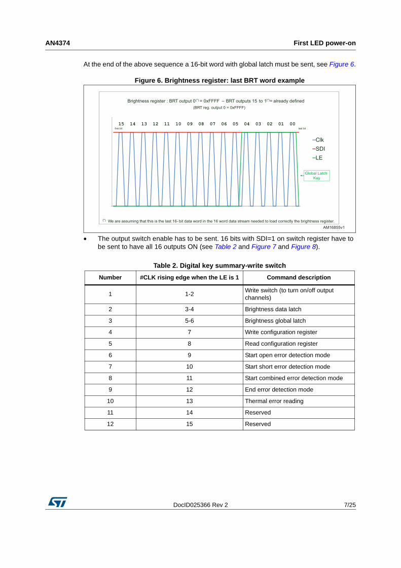
3 LED power-on at maximum current and 50% duty cycle
This example is similar to the previous one but, the configuration register value has been changed so to have the brightness counter at 12 bits and the current gain to the maximum. Besides, the brightness register set-up has been changed to have a PWM duty cycle of about 50%.
• In order to get the maximum LED current, configuration register bits from CFG-0 to CFG-6 need to be changed from 0 to 1. At the same time, to change the brightness counter from16 to 12 bits, CFG-15 has to be changed.
Table 3. Configuration register
Bit Definition R/W Description Default
CFG-0
Current gain adjustment
R/W6-bit DAC allows adjusting the device output current in 64 steps for each range (defined by CFG-6)
0
CFG-1 0
CFG-2 0
CFG-3 0
CFG-4 0
CFG-5 0
CFG-6 Current range R/W”0” low current range“1” high current range
0
CFG-7Error detection
modeR/W
“0” normal mode“1” reserved mode
0
CFG-8Shorted-LED
detection thresholds
R/W Programmable output
shorted-LED detection thresholds
CFG-9 CFG-8 Th. volt
00 0 1.8 V
0 1 2.5 V
CFG-9 R/W1 0 3 V
01 1 3.5 V
CFG-10Auto OFF shutdown
R/W“0” device always ON
”1” auto power shutdown active (auto OFF)0
CFG-11Output turn-on/off time
R/WProgrammable output rise and fall time (20% to 80%)
CFG-12 CFG-11 Turn-on Turn-off
00 0 30 ns 20 ns
0 1 100 ns 40 ns
CFG-12 R/W1 0 140 ns 80 ns
01 1 180 ns 150 ns
CFG-13 SDO delay R/WIf “0” no delay is present on SDOIf “1” the data is shifted out and synchronized with the falling edge of the CLK signal
0

LED power-on at maximum current and 50% duty cycle AN4374
10/25 DocID025366 Rev 2
Figure 9. Channel data and write switch
To carry on the changes both on the configuration register and on brightness register, the patterns are shown in Figure 10, Figure 11 and Figure 12.
Figure 10. LED1642GW and ALED1642GW configuration register
• In Figure 11 and Figure 12, as in the previous example, a 16-bit value has to be sent for each of 16 outputs, in particular, the first 15 patterns have a data latch (LE high for 3 CLK rising edges), last pattern has a global latch (LE high for 5 CLK rising edges). Unlike the first example, this time, the value to be programmed is 0x0800 to get 50% PWM duty cycle (12-bit counter) for all driver outputs:
CFG-14Gradual output
delayR/W
“0” a progressive delay is applied to output (10 ns per channel)”1” no delay is applied to output
0
CFG-1512/16 PWM
counterR/W
“0” to select 16-bit brightness register (65536 grayscale rightness steps).
“1” to select 12-bit brightness register (4096 grayscale brightness steps)
0
Table 3. Configuration register (continued)
Bit Definition R/W Description Default
0E0F 0C 0A0B0D 09 08 07 06 05 04 03 02 01 00
CLK
SDI
LE
16-bit data
AM16858v1
Clk
SDI
LE
15 14 13 12 11 10 09 08 07 06 05 04 03 02 01 00first bit last bit
CFG reg. in default condition except CFG -15/6 to 0=1: 12 bit PWM counter/gain=max/range=1(CFG reg.= 0x807F)
SDI and LE traces are overlapped
Data signal is high for clock rising edges 15, 06 to 00; LE is high for 7 clock rising edges
AM16859v1

DocID025366 Rev 2 11/25
AN4374 LED power-on at maximum current and 50% duty cycle
25
Figure 11. LED1642GW and ALED1642GW brightness register: first word example
Figure 12. LED1642GW and ALED1642GW brightness register: last word example
• As last pattern, the output switch power-on has to be sent. SDI=1 on switch register has to be sent 16 times (see previous example) to have all 16 outputs ON.
The result of the above eighteen 16-bit words is the LED power-on at ILED=36 mA and 50% duty cycle.
ClkSDILE
15 14 13 12 11 10 09 08 07 06 05 04 03 02 01 00first bit last bit
Brightness register : BRT output 15 (*) = 0x0800 – BRT outputs 14 to 0 (*) = TBD(BRT reg. output 15 = 0x0800)
(*) We are assuming that this is the last 16 -bit data word in the 16 word data stream needed to load correctly the brightness register.
Global Latch Key
AM16861v1
ClkSDILE
15 14 13 12 11 10 09 08 07 06 05 04 03 02 01 00first bit last bit
Brightness register : BRT Output 0 (*) = 0x0800 – BRT outputs 15 to 1(*) = already defined(BRT reg. output 0 = 0x0800)
(*) We are assuming that this is the last 16 -bit data word in the 16 word data stream needed to load correctly the brightness register.
Global Latch Key
AM16860v1

The PWCLK frequency choice AN4374
12/25 DocID025366 Rev 2
4 The PWCLK frequency choice
The PWCLK frequency must be selected to avoid visible flicker on the dimmed LEDs. The LED PWM frequency is linked to PWCLK frequency and in particular, the PWM frequency is the PWCLK frequency dived by 65536 (16-bit counter) or 4096 (12-bit counter) related to the configuration register set-up. To avoid LED flicker, usually, the PWM frequency must be higher than 100 Hz; to get this set-up, the PWCLK frequency has to be higher than 100x4096 = 410 kHz with CFG-15=1 (12-bit counter), we can round at 500 kHz.
In case of 16-bit counter, the minimum PWCLK frequency must be higher than 100x65536 = 6.5 MHz with CFG-15=0 (16-bit counter), we can round at 7 MHz. Figure 13 shows the internal PWM signal generation.
Figure 13. PWCLK counter and comparator
AM16862v1

DocID025366 Rev 2 13/25
AN4374 Output error detection
25
5 Output error detection
Stopping the normal activity of the display and turning on all driver channels allows the error detection to be performed and failed LED or display defects to be checked. The error detection is active when the CFG -7 bit in the configuration register is "0". The diagnostics is performed as shown in Figure 14:
Figure 14. Normal detection sequence
• The LED has to be selected turning on the relative channel on the switch register (powering on or off the output channels); the brightness register value for this channel cannot be zero.
• The appropriate digital key must be sent (seeTable 4 and Figure 15) to choose the type of detection (open, short or combined):
AM16863v1
Normal detection sequence
Read error detection result on SDO in 16 clock pulses after
detection end command
Turn on LED by PWCLK pulses for at least 1 µ s
Send open, short or combined error detection start command
by LE digital keys
Select LED to be turned on and checked in switch register
data; brightness for selected channels cannot be zero.
Select normal error detection modeon CFG register (bit 7 = “0”)
Send error detection end command by LE digital key

Output error detection AN4374
14/25 DocID025366 Rev 2
Figure 15. Digital key summary chart-detection
Table 4. Digital key summary-detection
Number #CLK rising edge when the LE is 1 Command description
1 1-2Write switch (to turn on/off output channels)
2 3-4 Brightness data latch
3 5-6 Brightness global latch
4 7 Write configuration register
5 8 Read configuration register
6 9 Start open error detection mode
7 10 Start short error detection mode
8 11 Start combined error detection mode
9 12 End error detection mode
10 13 Thermal error reading
11 14 Reserved
12 15 Reserved
CLK
LE
LE
LE
LE
LE
LE
LE
LE
LE
WWrite Switch
Data Latch
Global Latch
Write CR
Read CR
Start Open Error Detection
Start Short Error Detection
Start Combined Detection
End Error Detection
LE Thermal Error Reading
AM16864v1

DocID025366 Rev 2 15/25
AN4374 Output error detection
25
Figure 16. Error detection power-on timing
• After the error detection starts, the channel under test has to be turned on at least 1 µs (the LED is at the nominal current). Please note that, the output power-on depends on the PWCLK signal and in several applications this signal is not synchronized with the serial interface clock (CLK pin). Therefore, to be sure that, between the detection start and the detection end, the output power-on is 1 µs and moreover, that last power-on, in the interval, starts at least 0.5 µs before than detection end, it is suggested that the error detection should be performed just after the device startup (brightness counter reset) with all channels ON, before applying the PWCLK signal (see Figure 16).
• The result of the detection ("0" indicates a fault condition) is shifted out SDO in 16 clock pulses after the "detection end command" is provided, first output bit represents channel 15. Please note that (with SDO delay off) output 15 detection result is available just after the 1st clock pulse rising edge, so it can be sampled on the rising edge of the second clock pulse. In the same way, the output 0 detection result is available just after the 16th clock pulse rising edge, so it can be sampled on the rising edge of the 17th CLK pulse.
Pattern examples for error detection:
Figure 17. LED1642GW and ALED1642GW error detection: open detection start
0.5us Det.End
Det. Start
It must contain 1us output power ON
1us
SPI pattern
Output Current
x0000 < BRT < xFFFF
AM16865v1
ClkLE
15 14 13 12 11 10 09 08 07 06 05 04 03 02 01 00first bit last bit
Open detection start: 9 CLK rising edges when the LE is “1”
Data signal doesn't care; LE is high for 9 clock rising edges AM16866v1

Output error detection AN4374
16/25 DocID025366 Rev 2
Figure 18. LED1642GW and ALED1642GW error detection: short detection start
ClkLE
15 14 13 12 11 10 09 08 07 06 05 04 03 02 01 00first bit last bit
Short detection start: 10 CLK rising edges when the LE is “1”
Data signal doesn't care; LE is high for 10 clock rising edges AM16867v1

DocID025366 Rev 2 17/25
AN4374 Output error detection
25
Figure 19. LED1642GW and ALED1642GW error detection: combined detection start
Figure 20. LED1642GW and ALED1642GW error detection: detection end
Clk
LE
15 14 13 12 11 10 09 08 07 06 05 04 03 02 01 00first bit last bit
Combined detection start: 11 CLK rising edges when the LE is “1”
Data signal doesn't care; LE is high for 11 clock rising edges AM16868v1
ClkLE
15 14 13 12 11 10 09 08 07 06 05 04 03 02 01 00first bit last bit
Detection end: 12 CLK rising edges when the LE is “1” + 16 CLK rising edges for SDO data output
15 14 13 12 11 10 09 08 07 06 05 04 03 02 01 00
Data signal doesn't care; LE is high for 12 clock rising edges on first 16-bit word AM16869v1
Output error detection AN4374
18/25 DocID025366 Rev 2
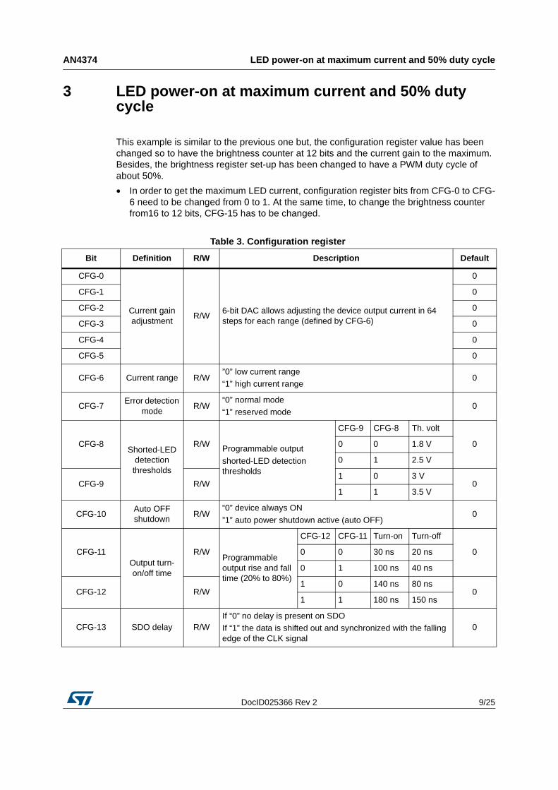
Error detection conditions:
During the error detection phases for each channel, the following parameters are checked:
• The output current in open detection mode (digital key: 9 CLK rising edges when LE is "1").
• The output voltage in short detection (digital key: 10 CLK rising edges when LE is "1").
• Both parameters (output voltage and current) in combined error detection mode (digital key: 11 CLK rising edges when LE is "1").
The thresholds for the error diagnostics are listed in Table 5:
Table 5. Diagnostics thresholds
Error detection modesChecked
malfunctionCFG-9 CFG-8
Thresholds (V)
Min. Typ. Max.
Open detection
Combined mode
Open line or output short to GND
x x Io ≤ 0.5 x Io_programmed
Short detection
Short on LED or short to VLED
0 0 1.15 Vo ≥ 1.8 2.05
0 1 2.25 Vo ≥ 2.5 2.75
1 0 2.75 Vo ≥ 3.0 3.25
1 1 3.25 Vo ≥ 3.5 3.80

DocID025366 Rev 2 19/25
AN4374 LED supply voltage
25
6 LED supply voltage
The choice of the LED supply voltage (VLED) must be carried out considering several parameters:
• The voltage drop across current generators (VO) must guarantee the desired current (see dedicated section in the datasheet).
• The maximum LED forward voltage (VF,max).
• The maximum power can be dissipated by the package under the application ambient conditions.
• The accuracy of the supply voltage itself (VLED can vary in a range and the minimum value should be considered).
Therefore the minimum LED supply voltage can be calculated as:
Equation 1
The LED supply voltage should be higher than VLED,min (to consider any fluctuation of the involved parameters) but not too high in order to keep low the power dissipation:
Equation 2
where VDD is the device voltage supply, IDD the device supply current, VO,i and ICHi are respectively the voltage drop across, the current generator i and the channel current i (the worst case is to consider all channels connected to LEDs at minimum VF and maximum VLED). In particular the power dissipation should be kept below the maximum power dissipation, defined as:
Equation 3
where Tj and Ta are respectively the junction and the ambient temperature, whereas Ɵja is the junction-to-ambient thermal resistance. Junction temperature should be maintained below 125 °C for industrial devices and below 150 °C for automotive grade devices. To summarize, the choice of the proper power supply must be a trade-off between the correct value assuring the desired LED current and the low power dissipation. In RGB applications, there can be a significant variability of the LED forward voltage (e.g. red LEDs have a lower forward voltage compared to green and blue ones).
In this case, the supply voltage must be chosen high enough to correctly switch on the LEDs with the highest forward voltage (green or blue). However this supply voltage is higher than the voltage required by red LEDs. Thus, the excess of voltage in the lines with red LEDs drops on the current generators, brings an increase of the power dissipation and loss of efficiency.
VLED,min Vo,typ VF,max+=
PD VDD IDD V0 i, ICHi⋅i l=
16
+⋅=
PD,max
Tj Ta–( )θja
----------------------=

LED supply voltage AN4374
20/25 DocID025366 Rev 2
Moreover, the extra-voltage across the red LED driving generators could cause an erroneous shorted-LED condition detection.
To avoid these drawbacks, two different approaches are possible:
• A resistor in series can be added to each red LED. In this manner, the voltage excess drops across the resistor instead of dropping across the current generators. This solution reduces significantly the power dissipated by the chip (lower Tj). However, the total power dissipation does not change and a remarkable part of the power wastes on the series resistor. This affects the efficiency and also raises the cost of the system due to the need to dissipate the generated heat.
• Another solution is to split the LED voltage rail: one for blue and green LEDs (VLED) and one for red LEDs (VLED_RED), which can be derived using a switching regulator. This solution is the most advantageous in terms of power dissipation. Voltage rails are tailored to LEDs they drive and the wasted power is significantly reduced as well as the heat produced.

DocID025366 Rev 2 21/25
AN4374 Higher current requests (outputs in parallel)
25
7 Higher current requests (outputs in parallel)
When the application requires to drive high power LEDs, the current demand could be higher than the current provided by a single channel. In this case, a higher current capability can be achieved by connecting together two or more channels (in accordance with the current value to be regulated). Generally, no stability issues are shown using this output connection but in any case a bypass capacitor on driver power supply (of about 1 uF) and in particular a bypass capacitor near LED anodes on VLED power supply rail (of about 47 uF) are strongly recommended.
8 PCB layout guidelines
The aim of this section is to provide some useful advice to design the application PCB. General suggestions for PCB design are always valid. Beyond general recommendations, there are some other important considerations, tailored for this device family especially to reduce as minimum as possible EMI effects and maintain good signal integrity.
Signal integrity and radiated/conducted immunity
– The external programming resistor between REXT and GND should be connected as closer as possible to the device.
– The serial bus should be routed on the board and shielded.
– Try to widen spaces among signal lines till routing restrictions allow.
– Do not draw traces closer than three times the dielectric height and moreover, the distance between the centers of two adjacent traces should be at least four times the trace width.
– Design the transmission line so that the conductor is as closer to the ground plane as possible. This technique couples the transmission line tightly to the ground plane and helps to decouple it from adjacent signals.
– All SPI signals should proceed to the same direction on the board by a bus (same electrical length) to avoid CLK/LE skew (CLK and SDI are re-synchronized device-by-device).
– As far as the serial bus is concerned, whenever it is possible, vias should be avoided, tracing all strips on a single layer. Provide a ground plane close to this layer. In case of an inner layer, insert the strips sandwiched between two GND surfaces. Reduce the length of connections from the main bus to the device chain (traces derived: stubs), especially for the CLK and PWCLK. Keep CLK and PWCLK traces as straight as possible (corners should be rounded).
– In the chain configuration, last device’s SDO signal has the maximum delay compared to CLK source signal (strip propagation delay), the controller compares a "delayed" SDO signal with a local "not delayed CLK" (check the set-up time and clock distribution).
– In case of poor digital signals or noise pick-up on SPI lines some low pass-filters represent a suitable solution to be implemented. The RC time constant must be chosen case-by-case considering CLK frequency and noise characteristics. For

PCB layout guidelines AN4374
22/25 DocID025366 Rev 2
example, with 1 MHz CLK frequency, an adequate value could be 15 ns (e.g. 100 Ohm + 150 pF).
Figure 21. Interface signal filtering
Radiated emission reduction (EMI)
– In order to decrease the electromagnetic noise during LED power-on/off, the driver output lines should follow the shortest path "power rail/LED/driver". Besides, in order to keep the system stability, a good electrolytic capacitor should be connected to the power supply rail as near as possible the LED anodes (the inductive LED power supply rail component should be compensated by added capacitance; in case of wide PCB, place more distributed capacitors). Another filter capacitor must be added to each driver power supply pin (VDD).
– Shorten as minimum as possible the SPI connection strips (from controller to LED driver).
Device thermal management
– In order to improve the power dissipation (to decrease the device working temperature), solder the package exposed pad (if available) to the board.
– In order to improve the thermal performance at least a 4-layer (e.g. 2S2P) PCB should be used.
– The copper area below the package thermal pad should be as large as possible, outside the package perimeter (using the package sides without pins).
– A reasonable number of vias must connect the copper area below the package to all available PCB layers especially just below the device package (e.g. 3x3 or 4x3 vias array) but also outside the package perimeter. Smaller and closely spaced
poor signal good signal
CLK, LE, etc. CLK, LE, etc.
Proper filtering to improve digital signal quality
AM16870v1

DocID025366 Rev 2 23/25
AN4374 PCB layout guidelines
25
vias could be a good solution.The best implementation is represented by copper filled vias.
– On each inner layer, a copper area must be provided for dissipation (if possible, at least 4 times wider than the package dimensions). A good condition is to have at least a power layer as an entire copper area (e.g. GND layer).
– Traces for pin connection must be enlarged till layout constrains allow.
– Several devices in power dissipation on the same board must be adequately spaced.

Revision history AN4374
24/25 DocID025366 Rev 2
9 Revision history
Table 6. Document revision history
Date Revision Changes
11-Oct-2013 1 Initial release.
14-Nov-2014 2
Updated title and introduction in cover page.Updated Figure 1: LED1642GW and ALED1642GW block diagram, Section 1: The LED1642GW and ALED1642GW basic circuit, Section 3: LED power-on at maximum current and 50% duty cycle and Section 5: Output error detection.Minor text changes.

DocID025366 Rev 2 25/25
AN4374
25
IMPORTANT NOTICE – PLEASE READ CAREFULLY
STMicroelectronics NV and its subsidiaries (“ST”) reserve the right to make changes, corrections, enhancements, modifications, and improvements to ST products and/or to this document at any time without notice. Purchasers should obtain the latest relevant information on ST products before placing orders. ST products are sold pursuant to ST’s terms and conditions of sale in place at the time of order acknowledgement.
Purchasers are solely responsible for the choice, selection, and use of ST products and ST assumes no liability for application assistance or the design of Purchasers’ products.
No license, express or implied, to any intellectual property right is granted by ST herein.
Resale of ST products with provisions different from the information set forth herein shall void any warranty granted by ST for such product.
ST and the ST logo are trademarks of ST. All other product or service names are the property of their respective owners.
Information in this document supersedes and replaces information previously supplied in any prior versions of this document.
© 2014 STMicroelectronics – All rights reserved