Embed Size (px)
Citation preview

July 2016 DocID029043 Rev 1 1/59
www.st.com
AN4840 Application note
SLLIMM™-nano 2nd series small low-loss intelligent molded module
Alessio Corsaro, Carmelo Parisi
Introduction The SLLIMM™-nano (small low-loss intelligent molded module) 2nd series is ST’s new family of very compact, high efficiency, dual-in-line intelligent power modules, with optional extra features. This family is designed with an improved package structure to achieve higher power levels in applications such as dishwashers, refrigerator compressors, air conditioning fans, dryers, draining and recirculation pumps and in low-power industrial applications, such as small fans, pumps, tools, etc.
This new series both complements and surpasses the original SLLIMM-nano series in terms of features, package types and flexibility.
The SLLIMM-nano 2nd series features:
expanded line-up to 5 A with trench field stop (TFS) IGBT technology for efficiency improvement
improved thermal performance (up to 40% thermal resistance reduction for 3 A size IPM)
slots for easy heatsink fixing
two different lead options: zig-zag leads (fully compatible with previous series) and in line leads (for a more compact size even)
double stand-off option: with or without
NTC thermistor embedded on all the product family
improved isolation rating to 1500 Vrms/min
The SLLIMM-nano 2nd product family combines optimized silicon chips, integrated in three main inverter blocks:
power stage
six very fast IGBTs
six freewheeling diodes
driving network
three high voltage gate drivers
gate resistors
three bootstrap diodes
protection and optional features
op-amp for advanced current sensing
comparator for fault protection against overcurrent and short-circuit
smart shutdown function
NTC thermistor
dead-time, interlocking function and undervoltage lockout
Thanks to its great compactness, the fully-isolated SLLIMM-nano 2 package (N2DIP) is the ideal solution for applications requiring reduced assembly space even with heatsink, without sacrificing thermal performance and reliability.
The aim of this application note is to provide a detailed description of the SLLIMM-nano 2nd series, providing the guidelines to motor drive designers for an efficient, reliable, and fast design when using this new product family from ST.
Contents AN4840
2/59 DocID029043 Rev 1
Contents
1 Differences between the SLLIMM-nano 1st and 2nd series ......... 6
1.1 Product synopsis ............................................................................... 7
1.2 Product line-up and nomenclature .................................................... 9
1.3 Internal circuit .................................................................................. 11
1.4 Absolute maximum ratings .............................................................. 11
2 Electrical characteristics and functions ...................................... 15
2.1 IGBTs .............................................................................................. 15
2.2 Freewheeling diodes ....................................................................... 15
2.3 High voltage gate drivers ................................................................ 15
2.3.1 Logic inputs ...................................................................................... 16
2.3.2 High voltage level shift...................................................................... 16
2.3.3 Undervoltage lockout ........................................................................ 17
2.3.4 Interlocking function and dead time .................................................. 18
2.3.5 Comparators for fault sensing .......................................................... 19
2.3.6 Short-circuit protection and smart shutdown function ...................... 19
2.3.7 Timing chart of short-circuit protection and smart shutdown function23
2.3.8 Current sensing shunt resistor selection .......................................... 25
2.3.9 RC filter network selection ................................................................ 25
2.3.10 Op-amp for advanced current sensing ............................................. 27
2.3.11 Bootstrap circuit ................................................................................ 28
2.3.12 Bootstrap capacitor selection ........................................................... 29
2.3.13 Initial bootstrap capacitor charging ................................................... 31
3 Package .......................................................................................... 33
3.1 Package structure ........................................................................... 33
3.2 Package outline and dimensions ..................................................... 35
3.3 Input and output pin description ...................................................... 35
4 Power loss and dissipation .......................................................... 39
4.1 Conduction power loss .................................................................... 39
4.2 Switching power loss ....................................................................... 42
4.3 Thermal impedance overview ......................................................... 43
4.4 Power loss calculation example ...................................................... 46
5 Design and mounting guidelines ................................................. 48
5.1 Typical circuit and recommendations .............................................. 48

AN4840 Contents
DocID029043 Rev 1 3/59
5.2 Layout suggestions ......................................................................... 50
5.2.1 General suggestions ......................................................................... 51
6 Mounting and handling instructions ............................................ 53
6.1 Heatsink mounting .......................................................................... 53
6.1.1 Mounting torque ................................................................................ 54
7 References ..................................................................................... 57
8 Revision history ............................................................................ 58

List of tables AN4840
4/59 DocID029043 Rev 1
List of tables
Table 1: Main differences ........................................................................................................................... 6 Table 2: SLLIMM-nano 2nd series line-up .................................................................................................. 9 Table 3: Inverter part................................................................................................................................. 11 Table 4: Control part (STGIPQ5C60T-Hyy) .............................................................................................. 13 Table 5: Supply voltage and operation behavior ...................................................................................... 13 Table 6: Total system................................................................................................................................ 13 Table 7: Integrated pull-down resistor values ........................................................................................... 16 Table 8: Interlocking function truth table ................................................................................................... 18 Table 9: Input and output pins .................................................................................................................. 35 Table 10: Cauer RC thermal network elements for SLLIMM-nano 2nd series ......................................... 46 Table 11: Document revision history ........................................................................................................ 58
AN4840 List of figures
DocID029043 Rev 1 5/59
List of figures
Figure 1: SLLIMM-nano 2nd series block diagram ..................................................................................... 8 Figure 2: SLLIMM-nano 2nd series nomenclature ................................................................................... 10 Figure 3: Internal circuit of the STGIPQ5C60T-Hyy ................................................................................. 11 Figure 4: Stray inductance components of the output stage .................................................................... 12 Figure 5: TC measurement point .............................................................................................................. 14 Figure 6: High voltage gate driver block diagram ..................................................................................... 16 Figure 7: Timing chart of the undervoltage lockout function ..................................................................... 17 Figure 8: Timing chart of dead time function ............................................................................................ 19 Figure 9: Equivalent resistance (NTC//RPD_SD) ..................................................................................... 21 Figure 10: Voltage of T / SD / OD pin according to NTC temperature ..................................................... 21 Figure 11: NTC thermistor position (top view) .......................................................................................... 22 Figure 12: Smart shutdown equivalent circuitry ........................................................................................ 22 Figure 13: Timing chart of smart shutdown function ................................................................................. 24 Figure 14: Re-enabling time constant, τB .................................................................................................. 24 Figure 15: Examples of SC protection circuit ........................................................................................... 25 Figure 16: Example of SC event ............................................................................................................... 26 Figure 17: 3-phase system ....................................................................................................................... 27 Figure 18: General advanced current sense scheme and waveforms ..................................................... 28 Figure 19: Bootstrap circuit ....................................................................................................................... 29 Figure 20: Bootstrap capacitor vs. switching frequency ........................................................................... 31 Figure 21: Initial bootstrap charging time.................................................................................................. 32 Figure 22: Images and internal view of N2DIP-26L package ................................................................... 34 Figure 23: N2DIP-26L package outline..................................................................................................... 35 Figure 24: Typical IGBT power loss .......................................................................................................... 39 Figure 25: Examples of IGBT and diode approximation of the output characteristic ............................... 40 Figure 26: Typical switching waveforms of the STGIPQ5H60T-Hyy ........................................................ 43 Figure 27: Equivalent thermal circuit with heatsink single IGBT .............................................................. 44 Figure 28: Thermal impedance Zth(j-c) curve for a single IGBT .............................................................. 45 Figure 29: Cauer RC equivalent circuit ..................................................................................................... 46 Figure 30: Maximum IC(RMS) current vs. fsw simulated curves.............................................................. 47 Figure 31: Typical application circuit ......................................................................................................... 49 Figure 32: Recommended snubber capacitor position ............................................................................. 51 Figure 33: General suggestions ................................................................................................................ 52 Figure 34: Recommended silicon grease thickness and positioning ........................................................ 54 Figure 35: Device flatness specification ................................................................................................... 55 Figure 36: Heatsink flatness specification ................................................................................................ 55 Figure 37: Recommended mounting screw fastening sequence ............................................................. 56
Differences between the SLLIMM-nano 1st and 2nd series
AN4840
6/59 DocID029043 Rev 1
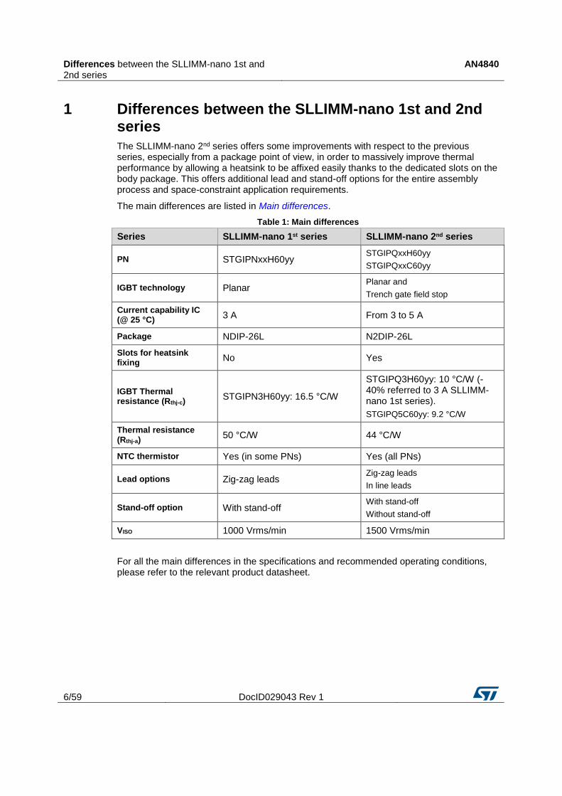
1 Differences between the SLLIMM-nano 1st and 2nd series
The SLLIMM-nano 2nd series offers some improvements with respect to the previous series, especially from a package point of view, in order to massively improve thermal performance by allowing a heatsink to be affixed easily thanks to the dedicated slots on the body package. This offers additional lead and stand-off options for the entire assembly process and space-constraint application requirements.
The main differences are listed in Main differences.
Table 1: Main differences
Series SLLIMM-nano 1st series SLLIMM-nano 2nd series
PN STGIPNxxH60yy STGIPQxxH60yy
STGIPQxxC60yy
IGBT technology Planar Planar and
Trench gate field stop
Current capability IC (@ 25 °C)
3 A From 3 to 5 A
Package NDIP-26L N2DIP-26L
Slots for heatsink fixing
No Yes
IGBT Thermal resistance (Rthj-c)
STGIPN3H60yy: 16.5 °C/W
STGIPQ3H60yy: 10 °C/W (-40% referred to 3 A SLLIMM-nano 1st series).
STGIPQ5C60yy: 9.2 °C/W
Thermal resistance (Rthj-a)
50 °C/W 44 °C/W
NTC thermistor Yes (in some PNs) Yes (all PNs)
Lead options Zig-zag leads Zig-zag leads
In line leads
Stand-off option With stand-off With stand-off
Without stand-off
VISO 1000 Vrms/min 1500 Vrms/min
For all the main differences in the specifications and recommended operating conditions, please refer to the relevant product datasheet.

AN4840 Differences between the SLLIMM-nano 1st and 2nd series
DocID029043 Rev 1 7/59
1.1 Product synopsis
The SLLIMM-nano 2nd series family has been designed to satisfy the requirements of a wide range of final applications up to 300 W, such as:
dishwashers
refrigerator compressors
air conditioning fans
dryers
draining and recirculation pumps
low power industrial applications
small fans, pumps and tools
The main features and integrated functions can be summarized as follows:
600 V, 3 and 5 A ratings
3-phase IGBT inverter bridge including:
six low-loss IGBTs
six low forward voltage drop and soft recovery freewheeling diodes
three control ICs for gate driving and protection including:
smart shutdown function
comparator for fault protection against overcurrent and short-circuit
op-amp for advanced current sensing
three integrated bootstrap diodes
interlocking function
undervoltage lockout
NTC thermistor
open emitter configuration for individual phase current sensing
very compact and fully isolated package
integrated gate resistors for optimum IGBT switching speed setting
proper biasing of gate driver
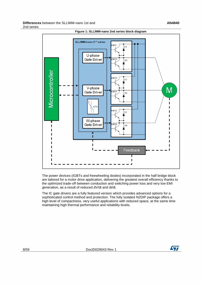
Figure 1 shows the block diagram of SLLIMM-nano 2nd series included in the inverter solution.
Differences between the SLLIMM-nano 1st and 2nd series
AN4840
8/59 DocID029043 Rev 1
Figure 1: SLLIMM-nano 2nd series block diagram
The power devices (IGBTs and freewheeling diodes) incorporated in the half bridge block are tailored for a motor drive application, delivering the greatest overall efficiency thanks to the optimized trade-off between conduction and switching power loss and very low EMI generation, as a result of reduced dV/dt and di/dt.
The IC gate drivers are a fully featured version which provides advanced options for a sophisticated control method and protection. The fully isolated N2DIP package offers a high level of compactness, very useful applications with reduced space, at the same time maintaining high thermal performance and reliability levels.
AN4840 Differences between the SLLIMM-nano 1st and 2nd series
DocID029043 Rev 1 9/59
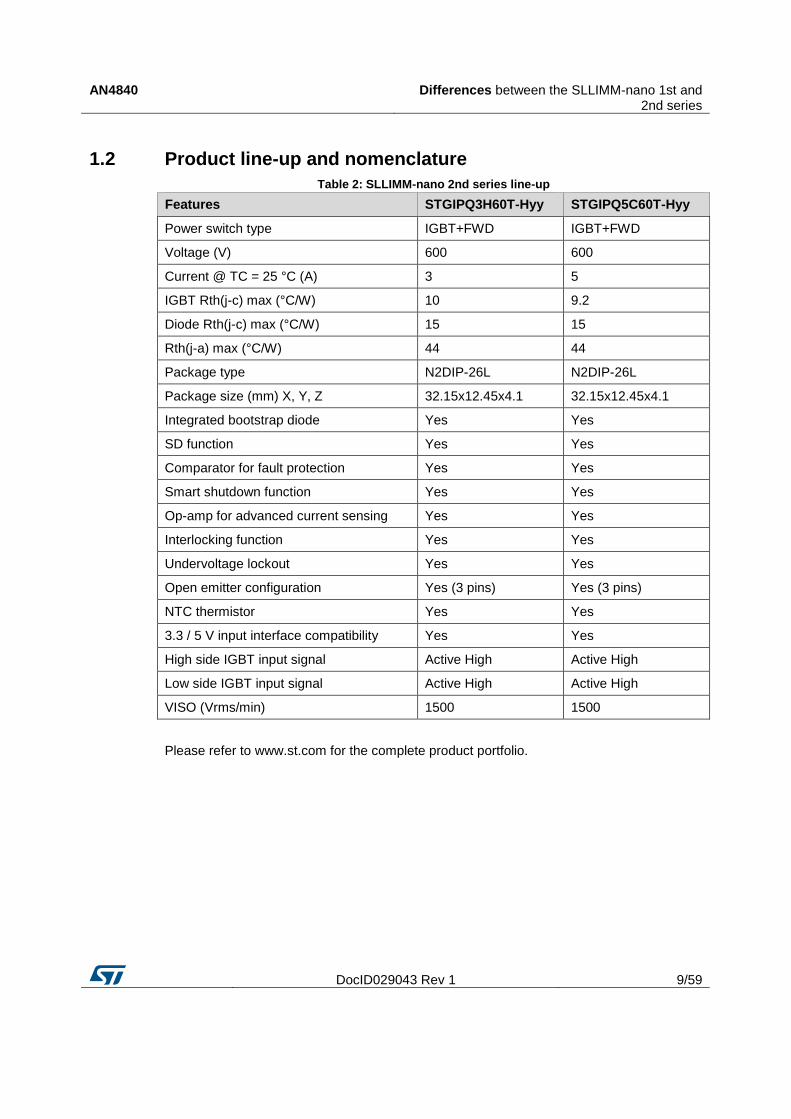
1.2 Product line-up and nomenclature
Table 2: SLLIMM-nano 2nd series line-up
Features STGIPQ3H60T-Hyy STGIPQ5C60T-Hyy
Power switch type IGBT+FWD IGBT+FWD
Voltage (V) 600 600
Current @ TC = 25 °C (A) 3 5
IGBT Rth(j-c) max (°C/W) 10 9.2
Diode Rth(j-c) max (°C/W) 15 15
Rth(j-a) max (°C/W) 44 44
Package type N2DIP-26L N2DIP-26L
Package size (mm) X, Y, Z 32.15x12.45x4.1 32.15x12.45x4.1
Integrated bootstrap diode Yes Yes
SD function Yes Yes
Comparator for fault protection Yes Yes
Smart shutdown function Yes Yes
Op-amp for advanced current sensing Yes Yes
Interlocking function Yes Yes
Undervoltage lockout Yes Yes
Open emitter configuration Yes (3 pins) Yes (3 pins)
NTC thermistor Yes Yes
3.3 / 5 V input interface compatibility Yes Yes
High side IGBT input signal Active High Active High
Low side IGBT input signal Active High Active High
VISO (Vrms/min) 1500 1500
Please refer to www.st.com for the complete product portfolio.
Differences between the SLLIMM-nano 1st and 2nd series
AN4840
10/59 DocID029043 Rev 1
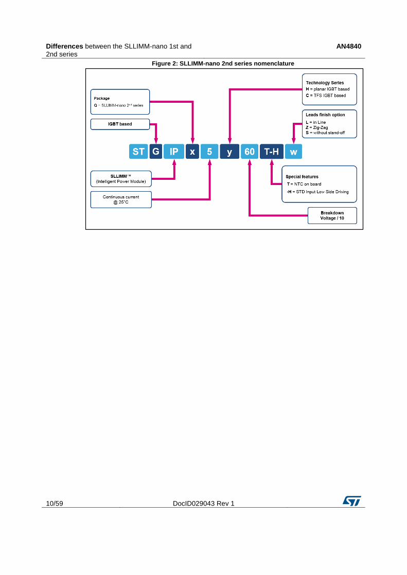
Figure 2: SLLIMM-nano 2nd series nomenclature
AN4840 Differences between the SLLIMM-nano 1st and 2nd series
DocID029043 Rev 1 11/59
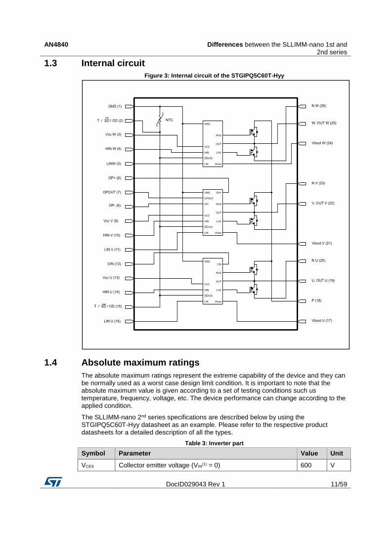
1.3 Internal circuit
Figure 3: Internal circuit of the STGIPQ5C60T-Hyy
1.4 Absolute maximum ratings
The absolute maximum ratings represent the extreme capability of the device and they can be normally used as a worst case design limit condition. It is important to note that the absolute maximum value is given according to a set of testing conditions such us temperature, frequency, voltage, etc. The device performance can change according to the applied condition.
The SLLIMM-nano 2nd series specifications are described below by using the STGIPQ5C60T-Hyy datasheet as an example. Please refer to the respective product datasheets for a detailed description of all the types.
Table 3: Inverter part
Symbol Parameter Value Unit
VCES Collector emitter voltage (VIN(1) = 0) 600 V
Differences between the SLLIMM-nano 1st and 2nd series
AN4840
12/59 DocID029043 Rev 1
Symbol Parameter Value Unit
IC Continuous collector current each IGBT 5 A
IC(2) Peak collector current each IGBT (less than 1ms) 10 A
PTOT Total dissipation at TC=25 °C each IGBT 13.6 W
Notes:
(1)Applied between HINx, LINx and GND for x = U, V, W. (2)Pulse width limited by max. junction temperature.
VCES: Collector emitter voltage
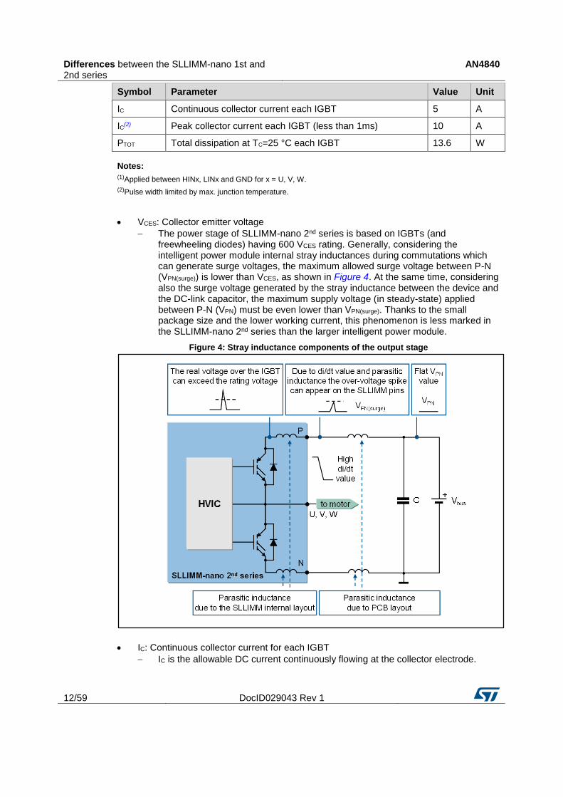
The power stage of SLLIMM-nano 2nd series is based on IGBTs (and freewheeling diodes) having 600 VCES rating. Generally, considering the intelligent power module internal stray inductances during commutations which can generate surge voltages, the maximum allowed surge voltage between P-N (VPN(surge)) is lower than VCES, as shown in Figure 4. At the same time, considering also the surge voltage generated by the stray inductance between the device and the DC-link capacitor, the maximum supply voltage (in steady-state) applied between P-N (VPN) must be even lower than VPN(surge). Thanks to the small package size and the lower working current, this phenomenon is less marked in the SLLIMM-nano 2nd series than the larger intelligent power module.
Figure 4: Stray inductance components of the output stage
IC: Continuous collector current for each IGBT
IC is the allowable DC current continuously flowing at the collector electrode.
AN4840 Differences between the SLLIMM-nano 1st and 2nd series
DocID029043 Rev 1 13/59
Table 4: Control part (STGIPQ5C60T-Hyy)
Symbol Parameter Value Unit
VCC Low voltage power supply -0.3 to 21 V
VBOOT Bootstrap voltage -0.3 to 620 V
VOUT Output voltage applied between OUTU, OUTV, OUTW and GND
Vboot - 21 to Vboot + 0.3 V
VCIN Comparator input voltage -0.3 to VCC + 0.3 V
VIN Logic input voltage applied between HINx, LINx and GND
-0.3 to 15 V
VT/ SD / OD Open drain voltage -0.3 to 15 V
∆ VOUT /dt Allowed output slew rate 50 V/ns
VCC: Low voltage power supply
VCC represents the supply voltage of the control part. Local filtering is recommended to enhance the SLLIMM-nano 2nd series noise immunity. Generally, the use of one electrolytic capacitor (with a greater value but not negligible ESR) and one smaller ceramic capacitor (hundreds of nF) that is faster than the electrolytic capacitor to provide current, is recommended. Please refer to Table 5 in order to properly drive the SLLIMM-nano 2nd series.
Table 5: Supply voltage and operation behavior
VCC voltage (typ. value)
Operating behavior
< 12 V As the voltage is lower than the UVLO threshold, the control circuit is not fully turned on. Perfect functionality cannot be guaranteed.
12 V – 15 V Typical operating conditions.
> 21 V Control circuit is destroyed.
Table 6: Total system
Symbol Parameter Value Unit
VISO Isolation withstand voltage applied between each pin and heatsink plate (AC voltage, t = 60 s)
1500 Vrms
Tj Power chips operating junction temperature -40 to 150 °C
TC Module case operation temperature -40 to 125 °C
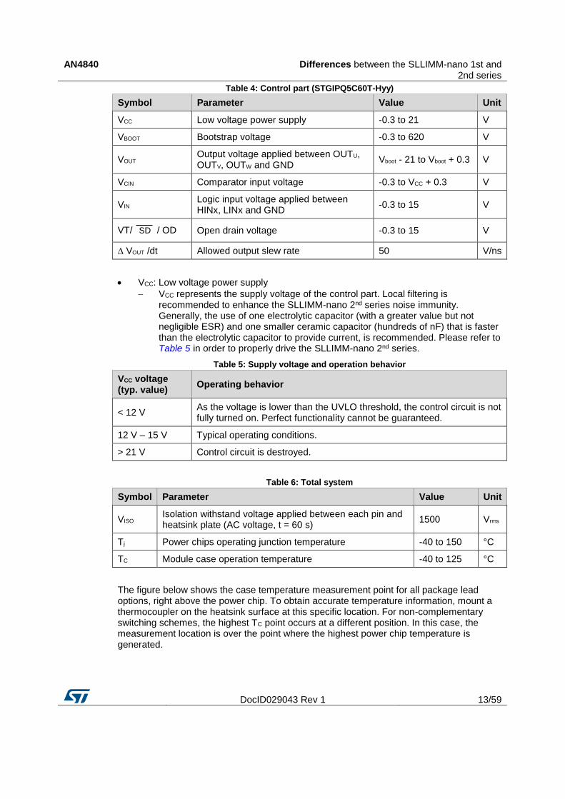
The figure below shows the case temperature measurement point for all package lead options, right above the power chip. To obtain accurate temperature information, mount a thermocoupler on the heatsink surface at this specific location. For non-complementary switching schemes, the highest TC point occurs at a different position. In this case, the measurement location is over the point where the highest power chip temperature is generated.
Differences between the SLLIMM-nano 1st and 2nd series
AN4840
14/59 DocID029043 Rev 1
Figure 5: TC measurement point

AN4840 Electrical characteristics and functions
DocID029043 Rev 1 15/59
2 Electrical characteristics and functions
In this section the main electrical characteristics of the power stage are discussed, together with a detailed description of all the SLLIMM-nano 2nd series functions.
2.1 IGBTs
The SLLIMM-nano 2nd series achieves power savings in the inverter stage thanks to the use of IGBTs manufactured with the proprietary advanced PowerMESH™ and trench field stop process. These power devices are optimized for typical motor control switching frequency and offer an excellent trade-off between voltage drop (VCE(sat)) and switching energy (Eon and Eoff), and therefore minimize the two major sources of energy loss (conduction and switching) reducing the environmental impact of daily-use equipment. A full analysis on the power loss of the complete system is reported in Section 4: "Power loss and dissipation".
2.2 Freewheeling diodes
ST's Turbo 2 ultrafast high voltage diodes have been selected for the SLLIMM-nano 2nd series and carefully tuned to achieve the best trr/VF trade-off and softness as freewheeling diodes in order to further improve the total performance of the inverter and significantly reduce the electromagnetic interference (EMI) in motor control applications, which are quite sensitive to this phenomena.
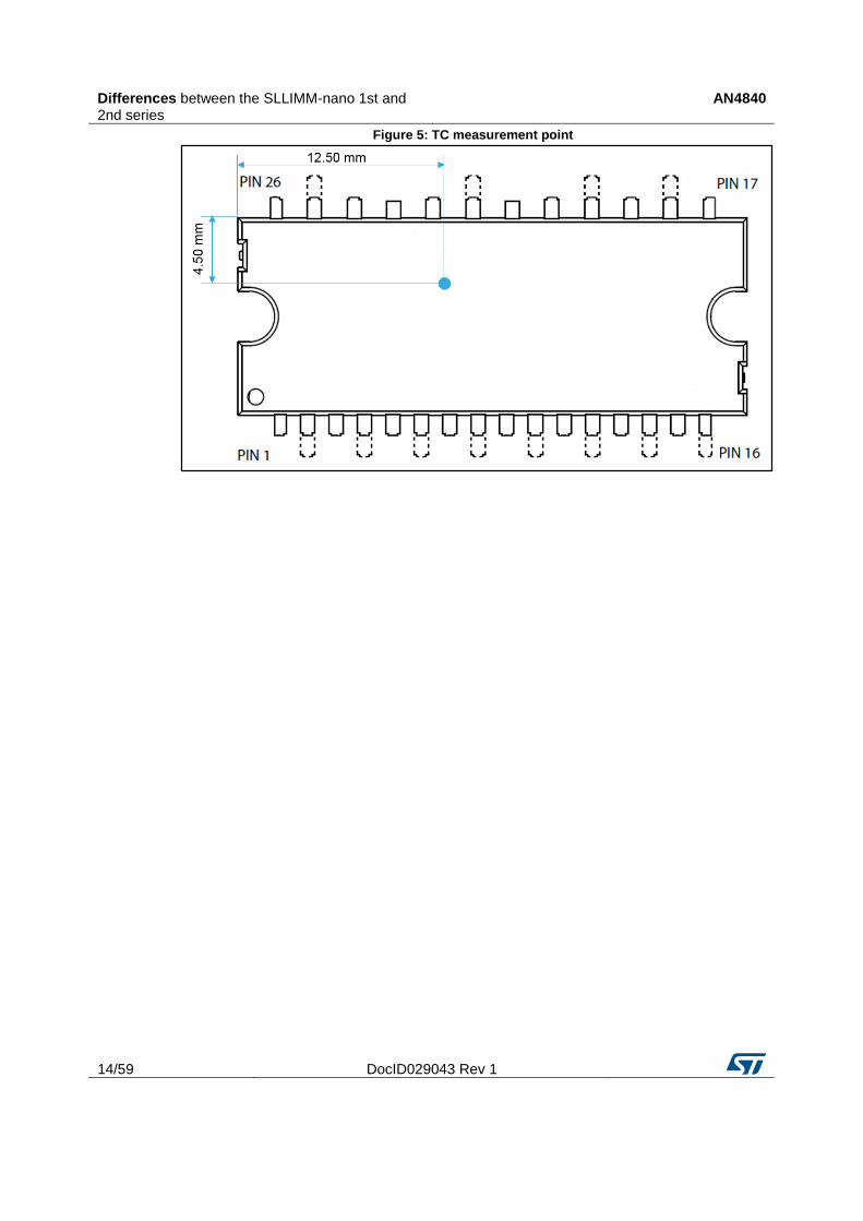
2.3 High voltage gate drivers
The SLLIMM-nano 2nd series is equipped with a versatile high voltage gate driver IC (HVIC), designed using BCD offline (bipolar, CMOS, and DMOS) technology and particularly suited to field oriented control (FOC) motor driving applications, and is able to provide all the functions and current capability necessary for high side and low side IGBT driving. This driver includes patented internal circuitry which replaces the external bootstrap diode.
Each high voltage gate driver chip controls two IGBTs in half bridge topology, offering basic functions such as interlocking, integrated bootstrap diode, and also advanced features such as smart shutdown (patented), fault comparator, and a dedicated high performance op-amp for advanced current sensing. A schematic summary of the features by device are listed in Table 2: "SLLIMM-nano 2nd series line-up".
In this application note, the main characteristics of a high voltage gate drive related to the SLLIMM-nano 2nd series are discussed. For further information, please refer to application note AN2738, available on st.com.
Electrical characteristics and functions AN4840
16/59 DocID029043 Rev 1
Figure 6: High voltage gate driver block diagram
2.3.1 Logic inputs
All the HINx and LINx logic inputs are provided with hysteresis (~1 V) for low noise sensitivity and are TTL/CMOS 3.3 V compatible. Thanks to this low voltage interface logic compatibility, the SLLIMM-nano 2nd series can be used with any type of high performance controller, such as microcontrollers, DSPs or FPGAs. As shown in the block diagram in Figure 6, the logic inputs have internal pull-down resistors in order to set a proper logic level in case of interruption in the logic lines. If logic inputs are left floating, the gate driver outputs LVG and HVG are set to low level. This simplifies the interface circuit by eliminating the six external resistors, thereby reducing cost, board space and component count.
The typical values of the integrated pull-down resistors are shown in Table 7:
Table 7: Integrated pull-down resistor values
Input pin Input pin logic Internal pull-down
High side gate driving
HINU, HINV, HINW Active high 375 kΩ
Low side gate driving
LINU, LINV, LINW Active high 375 kΩ
T / SD / OD shutdown Active low 50 kΩ
2.3.2 High voltage level shift
The built-in high voltage level shift allows direct connection between the low voltage control inputs and the high voltage power half bridge in any power application up to 600 V. It is obtained thanks to the BCD offline technology which integrates, in the same die, bipolar devices, low and medium voltage CMOS for analog and logic circuitry and high voltage
AN4840 Electrical characteristics and functions
DocID029043 Rev 1 17/59
DMOS transistors with a breakdown voltage in excess of 600 V. This key feature eliminates the need for external optocouplers, resulting in significant reduction in component count and power loss. Other advantages are high-frequency operation and short input-to-output delays.
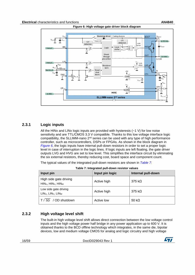
2.3.3 Undervoltage lockout
The SLLIMM-nano 2nd series supply voltage VCC is continuously monitored by undervoltage lockout (UVLO) circuitry which turns off the gate driver outputs when the supply voltage goes below the VCCH_th(off) threshold specified on the datasheet, and turns on the IC when the supply voltage goes above the VCCH_th(on) voltage. A hysteresis of about 1.5 V is provided for noise rejection purposes. A high voltage floating supply Vboot is also provided with similar undervoltage lockout circuitry. When the driver is in UVLO condition, both gate driver outputs are set to low level, setting the half bridge power stage output to high impedance.
The timing chart of the undervoltage lockout is plotted in Figure 7 and is based on the following steps:
t1: when the VCC supply voltage rises to the VCCH_th(on) threshold, the gate driver starts to work after the next input signal HIN/LIN is on. The circuit state becomes RESET.
t2: input signal HIN/LIN is on and the IGBT is turned on.
t3: when the VCC supply voltage goes below the VCCH_th(off) threshold, the UVLO event is detected. The IGBT is turned off in spite of the input signal HIN/LIN. The state of the circuit is now SET.
t4: the gate driver re-starts once the VCC supply voltage again rises to the VCCH_th(on) threshold.
t5: The input signal HIN/LIN is on and the IGBT is turned on again.
Figure 7: Timing chart of the undervoltage lockout function

Electrical characteristics and functions AN4840
18/59 DocID029043 Rev 1
2.3.4 Interlocking function and dead time
In order to prevent possible cross-conduction between high side and low side IGBTs, the SLLIMM-nano 2nd series provides interlocking functions, which is a logic operation setting both the outputs to low level when the inputs are simultaneously active, as shown in Table 8: "Interlocking function truth table". Even if an internal dead time is fixed as a default (180 ns typ.) between the falling edge transition of one driver output and the rising edge of the other output, the external dead time value set by application firmware is mandatory to avoid cross-conduction. External dead time is dominant over internal dead time, and it is recommended to set it in accordance with the datasheet value.
Table 8: Interlocking function truth table
Condition Logic input (VI) Outputs
LIN HIN LVG HVG
Interlocking
half bridge tri-state H H L L
0 “logic state”
half bridge tri-state L L L L
1 “logic state”
low side direct driving H L H L
1 “logic state”
high side direct driving L H L H
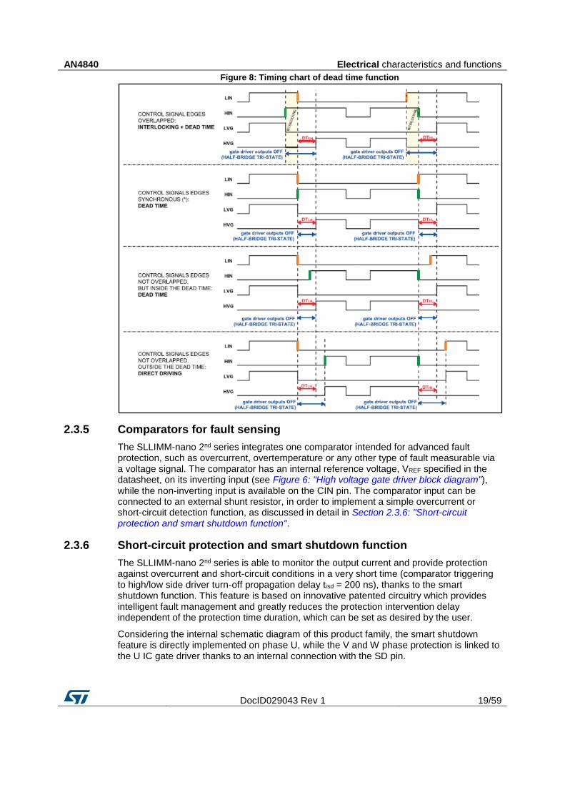
AN4840 Electrical characteristics and functions
DocID029043 Rev 1 19/59
Figure 8: Timing chart of dead time function
2.3.5 Comparators for fault sensing
The SLLIMM-nano 2nd series integrates one comparator intended for advanced fault protection, such as overcurrent, overtemperature or any other type of fault measurable via a voltage signal. The comparator has an internal reference voltage, VREF specified in the datasheet, on its inverting input (see Figure 6: "High voltage gate driver block diagram"), while the non-inverting input is available on the CIN pin. The comparator input can be connected to an external shunt resistor, in order to implement a simple overcurrent or short-circuit detection function, as discussed in detail in Section 2.3.6: "Short-circuit protection and smart shutdown function".
2.3.6 Short-circuit protection and smart shutdown function
The SLLIMM-nano 2nd series is able to monitor the output current and provide protection against overcurrent and short-circuit conditions in a very short time (comparator triggering to high/low side driver turn-off propagation delay tisd = 200 ns), thanks to the smart shutdown function. This feature is based on innovative patented circuitry which provides intelligent fault management and greatly reduces the protection intervention delay independent of the protection time duration, which can be set as desired by the user.
Considering the internal schematic diagram of this product family, the smart shutdown feature is directly implemented on phase U, while the V and W phase protection is linked to the U IC gate driver thanks to an internal connection with the SD pin.

Electrical characteristics and functions AN4840
20/59 DocID029043 Rev 1
As already mentioned in Section 2.3.5: "Comparators for fault sensing" and as shown in Figure 6: "High voltage gate driver block diagram", the comparator input can be connected to an external shunt resistor, RSHUNT, in order to implement a simple overcurrent detection function. An RC filter network (RSF and CSF) is necessary to prevent erroneous operation of the protection. The output signal of the comparator is fed to an integrated MOSFET with
the open drain available on the T / SD / OD pin, shared with the SD input. When the
comparator triggers, the U IC gate driver is set in shutdown state and its outputs are set to low level, leaving the half bridge in tri-state. In common overcurrent protection architectures, the comparator output is usually connected to the SD input and an external
RC network (RSD and CSD) is connected to this SD / OD line in order to provide a mono-
stable circuit which implements a protection time when a fault condition occurs.
Also, the outputs of the V and W IC gate drivers are set to low level, but not before the SD voltage reaches its low level threshold.
Finally, the smart shutdown structure allows immediate turn off of the U output gate driver
in case of fault, latching the turn-on of the open drain MOSFET, until the SD signal has
reached its lower threshold. After the SD signal goes below the lower threshold, the
open drain is switched off (see Figure 13).
Since the protection of the V and W phases is linked to the SD level, a delay time, mainly
due to the RSD-CSD network, is added for the shutdown of their outputs. Therefore, in order
to implement effective protection, the SD network must be designed with special
attention. For further details please refer to Section 2.3.7: "Timing chart of short-circuit protection and smart shutdown function".
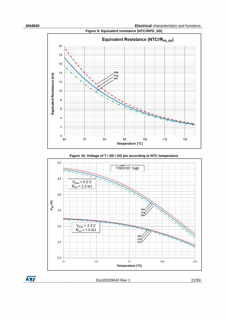
An NTC thermistor for temperature monitoring is internally connected in parallel to the SD
pin in order to perform temperature monitoring using the same T / SD / OD pin. The NTC
thermistor is in parallel with internal pull-down resistor (RPD_SD) and the equivalent resistance is shown in Figure 9. Both temperature monitoring and SD function can coexist on the same pin if a proper external pull-up resistor RSD is designed (refer to Figure 6).
Therefore, to avoid undesired shutdown, the T / SD / OD voltage should be kept higher
than the high-level logic threshold by setting the RSD to 1 kΩ or 2.2 kΩ for the 3.3 V or 5 V MCU power supplies, respectively (see Figure 10).
The block diagram of the smart shutdown architecture is depicted in Figure 12.
AN4840 Electrical characteristics and functions
DocID029043 Rev 1 21/59
Figure 9: Equivalent resistance (NTC//RPD_SD)
Figure 10: Voltage of T / SD / OD pin according to NTC temperature
Electrical characteristics and functions AN4840
22/59 DocID029043 Rev 1
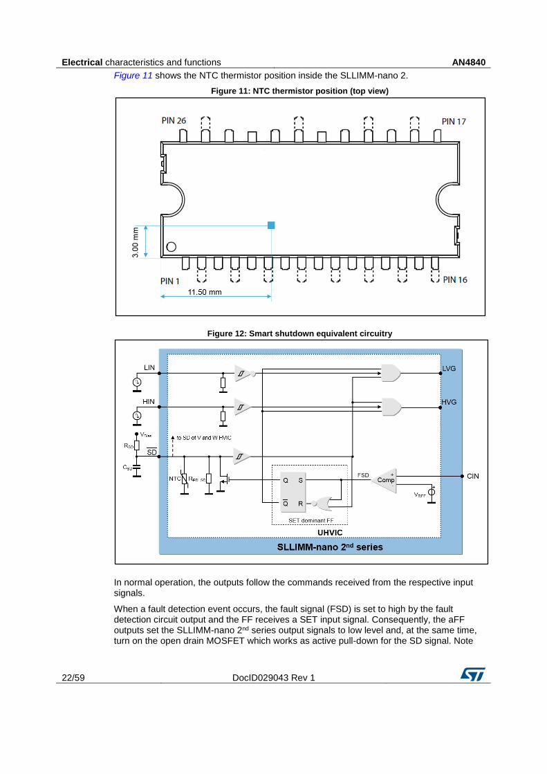
Figure 11 shows the NTC thermistor position inside the SLLIMM-nano 2.
Figure 11: NTC thermistor position (top view)
Figure 12: Smart shutdown equivalent circuitry
In normal operation, the outputs follow the commands received from the respective input signals.
When a fault detection event occurs, the fault signal (FSD) is set to high by the fault detection circuit output and the FF receives a SET input signal. Consequently, the aFF outputs set the SLLIMM-nano 2nd series output signals to low level and, at the same time, turn on the open drain MOSFET which works as active pull-down for the SD signal. Note

AN4840 Electrical characteristics and functions
DocID029043 Rev 1 23/59
that the gate driver outputs stay at low level until the SD pin has experienced both a
falling edge and a rising edge, although the fault signal could be returned to low level immediately after the fault sensing. In fact even if the FF is reset by the falling edge of the
SD input, the SD signal also works as enable for the outputs, thanks to the two AND
ports. Moreover, once the internal open drain transistor has been activated, due to the
latch, it cannot be turned off until the SD pin voltage reaches the low logic level. Note
that since the FF is SET dominant, oscillations of the SD pin are avoided if the fault
signal remains steady at high level.
2.3.7 Timing chart of short-circuit protection and smart shutdown function
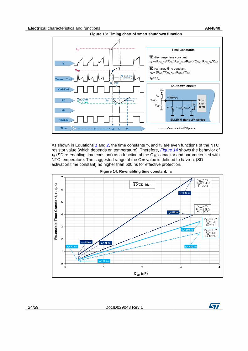
With reference to Figure 13, the short-circuit protection is based on the following steps:
t1: when the current is lower than the maximum allowed level, the SLLIMM-nano 2nd series works in normal operation.
t2: when the current reaches the maximum allowed level (ISC), an overcurrent/short-circuit event is detected and the protection is activated. The voltage across the shunt resistor, and then on the CIN pin, exceeds the VREF value, the comparator triggers, setting the U IC gate driver in shutdown state and both its outputs are set to low level leading the half bridge into tri-state. The smart shutdown (in the U IC gate driver) switches off the U phase IGBT gates (HVG, LVG) through a preferential path (200 ns typical internal delay time) and at the same time switches on the M1 internal MOSFET. The SD signal starts the discharge phase and its value drops with a time constant τA (SD activation time constant). The time constant of τA is given by:
Equation 1
t3: the SD signal reaches the lower threshold Vsd_L_THR, even the outputs of the V and W IC gate drivers are set to low and the control unit switches off all the HIN and LIN input. The smart shutdown is disabled (M1 off) and SD can rise with a time constant τB (SD re-enabling time constant), given by:
Equation 2
t4: when the SD signal reaches the upper threshold Vsd_H_THR, the system is re-
enabled.
Electrical characteristics and functions AN4840
24/59 DocID029043 Rev 1
Figure 13: Timing chart of smart shutdown function
As shown in Equations 1 and 2, the time constants τA and τB are even functions of the NTC resistor value (which depends on temperature). Therefore, Figure 14 shows the behavior of τB (SD re-enabling time constant) as a function of the CSD capacitor and parameterized with NTC temperature. The suggested range of the CSD value is defined to have τA (SD activation time constant) no higher than 500 ns for effective protection.
Figure 14: Re-enabling time constant, τB
AN4840 Electrical characteristics and functions
DocID029043 Rev 1 25/59
2.3.8 Current sensing shunt resistor selection
As previously discussed, the shunt resistors, RSHUNT, externally connected between the N pin and ground (see Figure 6) are used to implement the overcurrent detection. When the output current exceeds the short-circuit reference level (ISC), the CIN signal overtakes the VREF value and the short-circuit protection is active. For reliable and stable operation, the current sensing resistor should be of a high quality, low tolerance non-inductive type. In fact, stray inductance in the circuit, which includes the layout, the RC filter, and also the shunt resistor, must be minimized in order to avoid undesired short-circuit detection. For these reasons, the shunt resistor and filtering components must be placed as close as possible to the SLLIMM-nano 2nd series pins (for additional suggestions, refer to Section 5.2: "Layout suggestions"). The value of the current sense resistor can be calculated by following different guidelines, functions of the design specifications, or requirements. A common criterion is presented here based on the following steps:
Defining the overcurrent threshold value (ISC). For example, it can be fixed considering the IGBT typical working current in the application and adding 20-30% as overcurrent.
Calculation of the shunt resistor value according to the conditioning network. An example of the conditioning network is shown in Figure 18.
Selection of the closest shunt resistor commercial value.
Equation 3
2.3.9 RC filter network selection
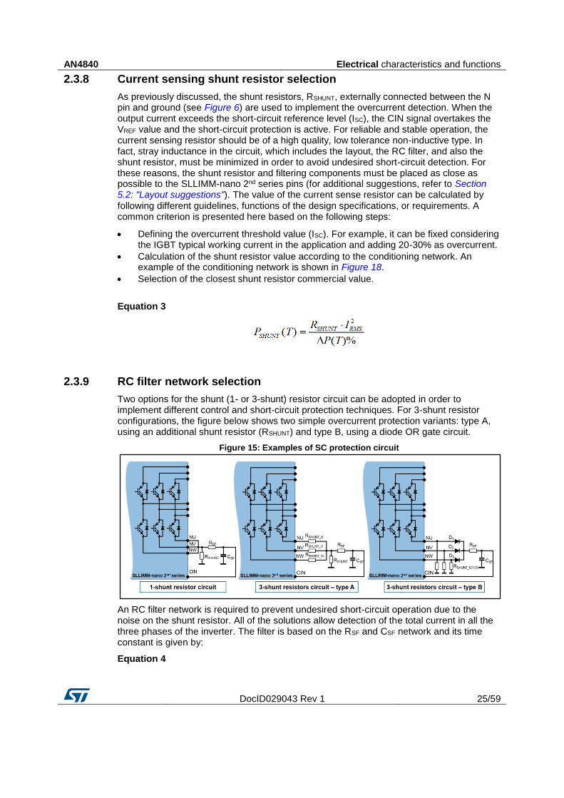
Two options for the shunt (1- or 3-shunt) resistor circuit can be adopted in order to implement different control and short-circuit protection techniques. For 3-shunt resistor configurations, the figure below shows two simple overcurrent protection variants: type A, using an additional shunt resistor (RSHUNT) and type B, using a diode OR gate circuit.
Figure 15: Examples of SC protection circuit
An RC filter network is required to prevent undesired short-circuit operation due to the noise on the shunt resistor. All of the solutions allow detection of the total current in all the three phases of the inverter. The filter is based on the RSF and CSF network and its time constant is given by:
Equation 4
Electrical characteristics and functions AN4840
26/59 DocID029043 Rev 1
In addition to the RC time constant, the turn-off propagation delay of the gate driver, tisd (specified in the datasheet) and the IGBT turn-off time, toff, (in the range of tens of ns), must be considered in the total delay time (tTotal), which is the time necessary to completely switch off the IGBT once the short-circuit event is detected. Therefore, the tTotal is calculated as follows:
Equation 5
and the tSF is recommended to be set no higher than 1 μs.
In the case of a 3-shunt resistor circuit, a specific control technique can be implemented by using the three shunt resistors (RSHUNT_U, RSHUNT_V and RSHUNT_W) able to monitor each phase of current.
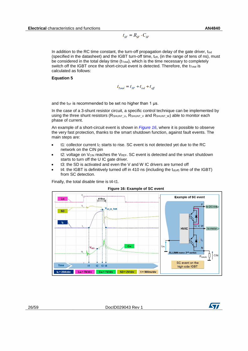
An example of a short-circuit event is shown in Figure 16, where it is possible to observe the very fast protection, thanks to the smart shutdown function, against fault events. The main steps are:
t1: collector current IC starts to rise. SC event is not detected yet due to the RC network on the CIN pin
t2: voltage on VCIN reaches the VREF. SC event is detected and the smart shutdown starts to turn off the U IC gate driver.
t3: the SD is activated and even the V and W IC drivers are turned off
t4: the IGBT is definitively turned off in 410 ns (including the td(off) time of the IGBT) from SC detection.
Finally, the total disable time is t4-t1.
Figure 16: Example of SC event
AN4840 Electrical characteristics and functions
DocID029043 Rev 1 27/59
2.3.10 Op-amp for advanced current sensing
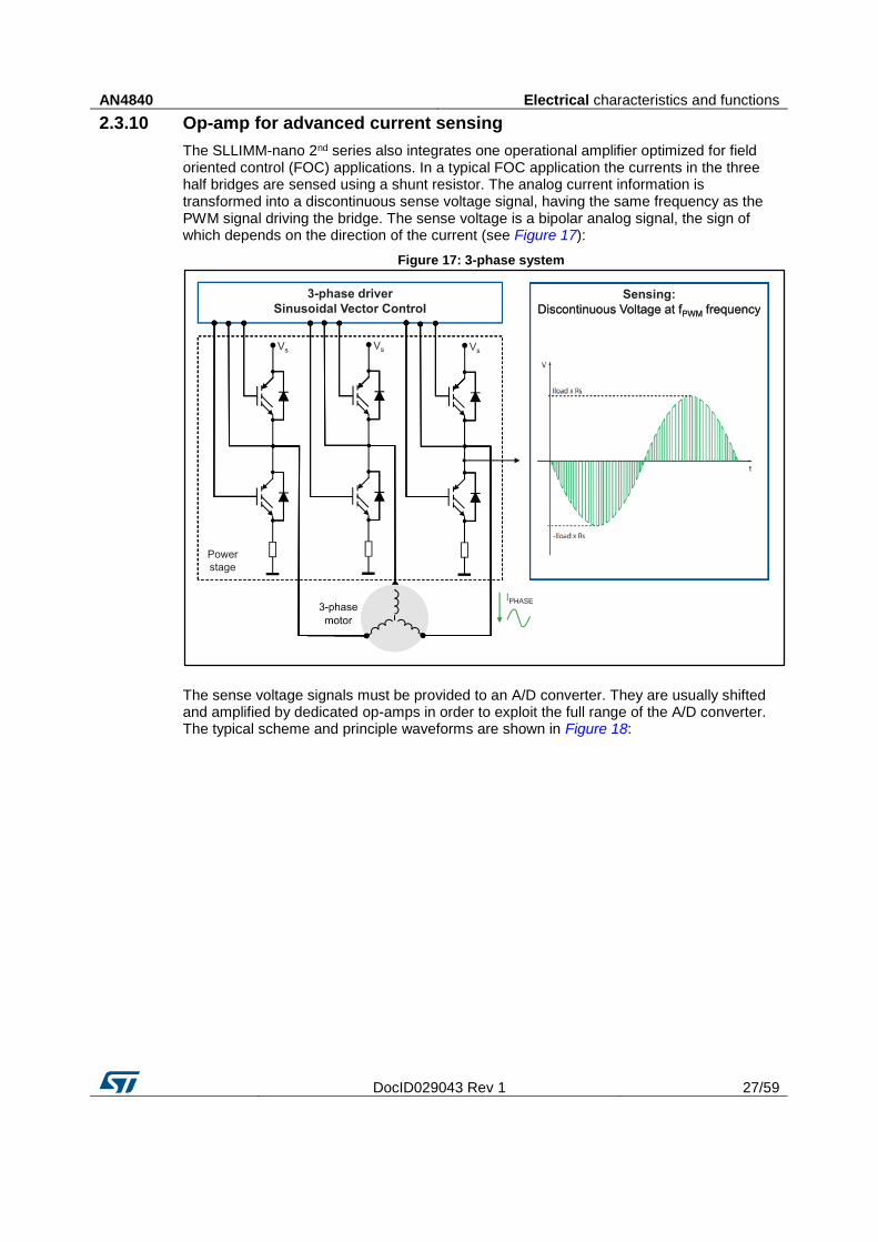
The SLLIMM-nano 2nd series also integrates one operational amplifier optimized for field oriented control (FOC) applications. In a typical FOC application the currents in the three half bridges are sensed using a shunt resistor. The analog current information is transformed into a discontinuous sense voltage signal, having the same frequency as the PWM signal driving the bridge. The sense voltage is a bipolar analog signal, the sign of which depends on the direction of the current (see Figure 17):
Figure 17: 3-phase system
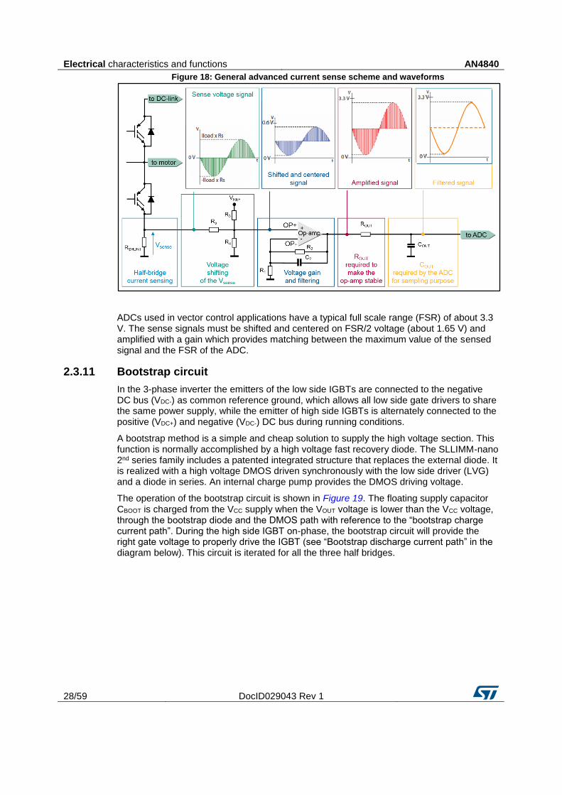
The sense voltage signals must be provided to an A/D converter. They are usually shifted and amplified by dedicated op-amps in order to exploit the full range of the A/D converter. The typical scheme and principle waveforms are shown in Figure 18:
Electrical characteristics and functions AN4840
28/59 DocID029043 Rev 1
Figure 18: General advanced current sense scheme and waveforms
ADCs used in vector control applications have a typical full scale range (FSR) of about 3.3 V. The sense signals must be shifted and centered on FSR/2 voltage (about 1.65 V) and amplified with a gain which provides matching between the maximum value of the sensed signal and the FSR of the ADC.
2.3.11 Bootstrap circuit
In the 3-phase inverter the emitters of the low side IGBTs are connected to the negative DC bus (VDC-) as common reference ground, which allows all low side gate drivers to share the same power supply, while the emitter of high side IGBTs is alternately connected to the positive (VDC+) and negative (VDC-) DC bus during running conditions.
A bootstrap method is a simple and cheap solution to supply the high voltage section. This function is normally accomplished by a high voltage fast recovery diode. The SLLIMM-nano 2nd series family includes a patented integrated structure that replaces the external diode. It is realized with a high voltage DMOS driven synchronously with the low side driver (LVG) and a diode in series. An internal charge pump provides the DMOS driving voltage.
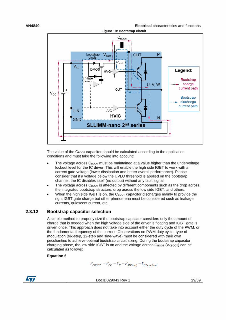
The operation of the bootstrap circuit is shown in Figure 19. The floating supply capacitor CBOOT is charged from the VCC supply when the VOUT voltage is lower than the VCC voltage, through the bootstrap diode and the DMOS path with reference to the “bootstrap charge current path”. During the high side IGBT on-phase, the bootstrap circuit will provide the right gate voltage to properly drive the IGBT (see “Bootstrap discharge current path” in the diagram below). This circuit is iterated for all the three half bridges.
AN4840 Electrical characteristics and functions
DocID029043 Rev 1 29/59
Figure 19: Bootstrap circuit
The value of the CBOOT capacitor should be calculated according to the application conditions and must take the following into account:
The voltage across CBOOT must be maintained at a value higher than the undervoltage lockout level for the IC driver. This will enable the high side IGBT to work with a correct gate voltage (lower dissipation and better overall performance). Please consider that if a voltage below the UVLO threshold is applied on the bootstrap channel, the IC disables itself (no output) without any fault signal.
The voltage across CBOOT is affected by different components such as the drop across the integrated bootstrap structure, drop across the low side IGBT, and others.
When the high side IGBT is on, the CBOOT capacitor discharges mainly to provide the right IGBT gate charge but other phenomena must be considered such as leakage currents, quiescent current, etc.
2.3.12 Bootstrap capacitor selection
A simple method to properly size the bootstrap capacitor considers only the amount of charge that is needed when the high voltage side of the driver is floating and IGBT gate is driven once. This approach does not take into account either the duty cycle of the PWM, or the fundamental frequency of the current. Observations on PWM duty cycle, type of modulation (six-step, 12-step and sine-wave) must be considered with their own peculiarities to achieve optimal bootstrap circuit sizing. During the bootstrap capacitor charging phase, the low side IGBT is on and the voltage across CBOOT (VCBOOT) can be calculated as follows:
Equation 6

Electrical characteristics and functions AN4840
30/59 DocID029043 Rev 1
where:
VCC: supply voltage of gate driver
VF: bootstrap diode forward voltage drop
VCE(sat)max: maximum emitter collector voltage drop of the low side IGBT
VRDS(on): DMOS voltage drop
The dimension of the bootstrap capacitance CBOOT value is based on the minimum voltage drop (ΔVCBOOT) to guarantee when the high side IGBT is on, and it must be:
Equation 7
under the condition:
Equation 8
where:
VGE(min): minimum gate emitter voltage of high side IGBT
VBS_th(on): bootstrap turn-on undervoltage threshold (maximum value, see datasheet)
Considering the factors contributing to a decrease in VCBOOT, the total charge supplied by the bootstrap capacitor (during high side on phase) is:
Equation 9
where:
QGATE: total IGBT gate charge
ILKGE: IGBT gate emitter leakage current
IQBO: bootstrap circuit quiescent current
ILK: bootstrap circuit leakage current
ILKDiode: bootstrap diode leakage current
ILKCap: bootstrap capacitor leakage current (relevant when using an electrolytic capacitor but can be ignored if other types of capacitors are used)
tHon: high side on time
QLS: charge required by the internal level shifters
Finally, the minimum size of the bootstrap capacitor is:
Equation 10
AN4840 Electrical characteristics and functions
DocID029043 Rev 1 31/59
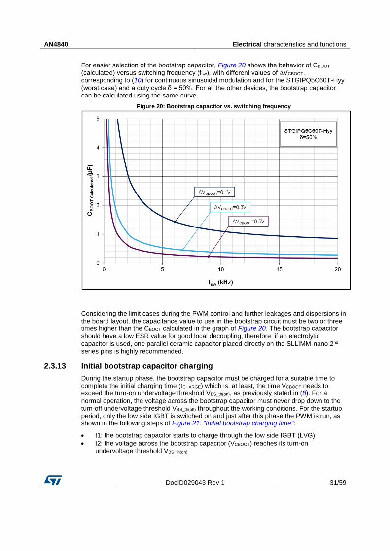
For easier selection of the bootstrap capacitor, Figure 20 shows the behavior of CBOOT (calculated) versus switching frequency (fsw), with different values of ∆VCBOOT, corresponding to (10) for continuous sinusoidal modulation and for the STGIPQ5C60T-Hyy (worst case) and a duty cycle δ = 50%. For all the other devices, the bootstrap capacitor can be calculated using the same curve.
Figure 20: Bootstrap capacitor vs. switching frequency
Considering the limit cases during the PWM control and further leakages and dispersions in the board layout, the capacitance value to use in the bootstrap circuit must be two or three times higher than the CBOOT calculated in the graph of Figure 20. The bootstrap capacitor should have a low ESR value for good local decoupling, therefore, if an electrolytic capacitor is used, one parallel ceramic capacitor placed directly on the SLLIMM-nano 2nd series pins is highly recommended.
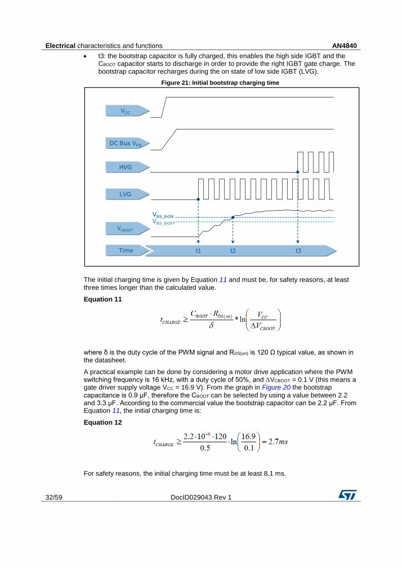
2.3.13 Initial bootstrap capacitor charging
During the startup phase, the bootstrap capacitor must be charged for a suitable time to complete the initial charging time (tCHARGE) which is, at least, the time VCBOOT needs to exceed the turn-on undervoltage threshold VBS_th(on), as previously stated in (8). For a normal operation, the voltage across the bootstrap capacitor must never drop down to the turn-off undervoltage threshold VBS_th(off) throughout the working conditions. For the startup period, only the low side IGBT is switched on and just after this phase the PWM is run, as shown in the following steps of Figure 21: "Initial bootstrap charging time":
t1: the bootstrap capacitor starts to charge through the low side IGBT (LVG)
t2: the voltage across the bootstrap capacitor (VCBOOT) reaches its turn-on undervoltage threshold VBS_th(on)
Electrical characteristics and functions AN4840
32/59 DocID029043 Rev 1
t3: the bootstrap capacitor is fully charged, this enables the high side IGBT and the CBOOT capacitor starts to discharge in order to provide the right IGBT gate charge. The bootstrap capacitor recharges during the on state of low side IGBT (LVG).
Figure 21: Initial bootstrap charging time
The initial charging time is given by Equation 11 and must be, for safety reasons, at least three times longer than the calculated value.
Equation 11
where δ is the duty cycle of the PWM signal and RDS(on) is 120 Ω typical value, as shown in the datasheet.
A practical example can be done by considering a motor drive application where the PWM switching frequency is 16 kHz, with a duty cycle of 50%, and ∆VCBOOT = 0.1 V (this means a gate driver supply voltage VCC = 16.9 V). From the graph in Figure 20 the bootstrap capacitance is 0.9 μF, therefore the CBOOT can be selected by using a value between 2.2 and 3.3 μF. According to the commercial value the bootstrap capacitor can be 2.2 μF. From Equation 11, the initial charging time is:
Equation 12
For safety reasons, the initial charging time must be at least 8.1 ms.
AN4840 Package
DocID029043 Rev 1 33/59
3 Package
The N2DIP is a dual-in-line transfer mold package available in a 26-lead version (N2DIP-26L) capable of meeting the demanding cost and size requirements of consumer appliance inverters. It consists of a copper lead frame with power stage and control stage soldered on it and housed using the transfer molding process. The excellent thermal properties of the copper allows good heat distribution and heat transfer. The thickness and the layout of the lead frames has been optimized to further reduce thermal resistance compared to the previous series.
Furthermore, this new package is designed to allow a better and more easily screwed-on heatsink thanks to the dedicated slots for screws placed on the short side of the package. This characteristic allows the SLLIMM-nano 2nd series to be used in higher power level applications than the 1st series. The new series is offered in two lead options: zig-zag and in-line leads.
The zig-zag leads option is pin-to-pin compatible with previous series for a natural extension targeting higher power-level sockets.
The new in-line leads option offers further compactness thanks to the aligned leads and satisfies the needs of applications with space constraint requirements.
Both lead options have been designed to maximize the distance between the high voltage and low voltage pins, by placing the relevant pins on the opposite side of the package. This is mainly useful to keep a safe distance between high voltage and low voltage pins and for easy PCB layout.
3.1 Package structure
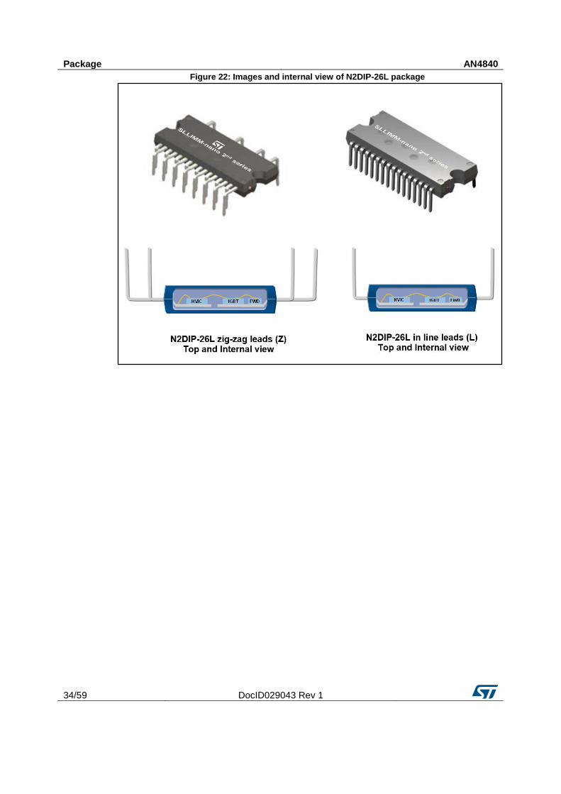
Figure 22 shows images and the internal structure of the N2DIP-26L package.
Package AN4840
34/59 DocID029043 Rev 1
Figure 22: Images and internal view of N2DIP-26L package
AN4840 Package
DocID029043 Rev 1 35/59
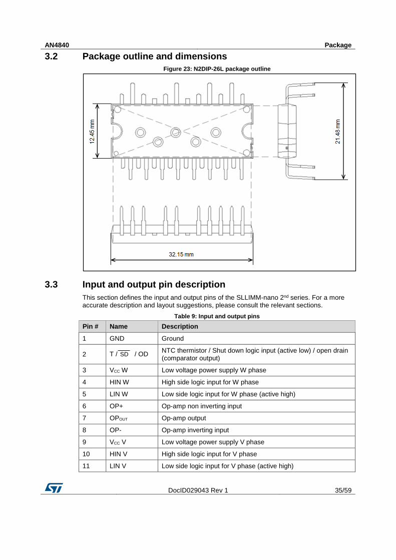
3.2 Package outline and dimensions
Figure 23: N2DIP-26L package outline
3.3 Input and output pin description
This section defines the input and output pins of the SLLIMM-nano 2nd series. For a more accurate description and layout suggestions, please consult the relevant sections.
Table 9: Input and output pins
Pin # Name Description
1 GND Ground
2 T / SD / OD NTC thermistor / Shut down logic input (active low) / open drain (comparator output)
3 VCC W Low voltage power supply W phase
4 HIN W High side logic input for W phase
5 LIN W Low side logic input for W phase (active high)
6 OP+ Op-amp non inverting input
7 OPOUT Op-amp output
8 OP- Op-amp inverting input
9 VCC V Low voltage power supply V phase
10 HIN V High side logic input for V phase
11 LIN V Low side logic input for V phase (active high)

Package AN4840
36/59 DocID029043 Rev 1
Pin # Name Description
12 CIN Comparator input
13 VCC U Low voltage power supply U phase
14 HIN U High side logic input for U phase
15 T / SD / OD NTC thermistor / Shut down logic input (active low) / open drain (comparator output)
16 LIN U Low side logic input for U phase (active high)
17 Vboot U Bootstrap voltage for U phase
18 P Positive DC input
19 U, OUT U U phase output
20 N U Negative DC input for U phase
21 Vboot V Bootstrap voltage for V phase
22 V, OUT V V phase output
23 N V Negative DC input for V phase
24 Vboot W Bootstrap voltage for W phase
25 W, OUT W W phase output
26 N W Negative DC input for W phase
High side bias voltage pins / high side bias voltage reference
Pins: VbootU-U, VbootV-V, VbootW-W
The bootstrap section is designed to realize a simple and efficient floating power supply, in order to provide the gate voltage signal to the high side IGBTs.
The SLLIMM-nano 2nd series family integrates the bootstrap diodes. This helps customers to reduce cost, board space, and number of components.
The advantage of the ability to bootstrap the circuit scheme is that no external power supplies are required for the high side IGBTs.
Each bootstrap capacitor is charged from the VCC supply during the on-state of the corresponding low side IGBT.
To prevent malfunctions caused by noise and ripple in supply voltage, a good quality (low ESR, low ESL) filter capacitor should be mounted close to these pins.
The value of bootstrap capacitors is strictly related to the application conditions. Please consult Section 2.3.11: "Bootstrap circuit" for more information.
Gate driver bias voltage
Pins: VCC U, VCC V, VCC W
Control supply pins for the built-in ICs.
To prevent malfunctions caused by noise and ripple in the supply voltage, a good quality (low ESR, low ESL) filter capacitors should be mounted close to these pins.
Gate drive supply ground
Pin: GND
AN4840 Package
DocID029043 Rev 1 37/59
Ground reference pin for the built-in ICs.
To avoid noise influences, the main power circuit current should not be allowed to flow through this pin (see Section 5.2: "Layout suggestions").
Signal input
Pins: HINU, HINV, HINW; LINU, LINV, LINW:
These pins control the operation of the built-in IGBTs.
The signal logic of HINx and LINx pins is active high. The IGBT associated with each of these pins is turned on when a sufficient logic (higher than a specific threshold) voltage is applied to these pins.
The wiring of each input should be as short as possible to protect the device against noise influences. RC coupling circuits should be adopted for the prevention of input signal oscillation. Suggested values are R=100 Ω and C=1 nF.
Internal non-inverting comparator
Pin: CIN
The current sensing shunt resistor, connected on each phase leg, could be used by the internal comparator (pin CIN) to detect short-circuit current.
The shunt resistor should be selected to meet the detection levels matched for the specific application.
An RC filter (typically ~1 us) should be connected to the CIN pin to eliminate noise.
The connection length between the shunt resistor and CIN pin should be minimized.
If a voltage signal, higher than the specified VREF (see datasheet), is applied to this
pin, the SLLIMM-nano 2nd series automatically shuts down and the T / SD / OD pin is
pulled down (to inform the microcontroller).
NTC thermistor / Shutdown / open drain
Pins: T / SD / OD
There are two available pins of T / SD / OD which are exactly the same. They are
placed on the opposite ends of the package in order to offer higher flexibility to the PCB layout. It is sufficient to use only one of two pins for the proper functioning of the device.
The T / SD / OD pins work as an enable/disable pins.
The signal logic of T / SD / OD pins are active low. The SLLIMM-nano 2nd series
shuts down if a voltage lower than a specific threshold is applied to these pins, leading each half bridge in tri-state.
The T / SD / OD status is connected also to the internal comparator status (Section
2.3.6: "Short-circuit protection and smart shutdown function"). When the comparator triggers, the T /SD / OD pin is pulled down acting as a FAULT pin.
The T / SD / OD, when pulled down by the comparator, are open drain configured.
The T / SD / OD voltage should be pulled up to the 3.3 V or 5 V logic power supply
through a pull-up resistor.
The T / SD / OD pin can be used for temperature monitoring as well, thanks to the
co-packaged NTC thermistor. A resistor RSD of 1 kΩ or 2.2 kΩ for the 3.3 V or 5 V MCU power supplies, respectively, is required to avoid undesired shutdown, along

Package AN4840
38/59 DocID029043 Rev 1
with a capacitor CSD no higher than 1 us for effective protection. For further details, refer to Section 2.3.7: "Timing chart of short-circuit protection and smart shutdown function".
Integrated operational amplifier
Pins: OP+, OP-, OPOUT
The op-amp is completely uncommitted.
The op-amp performances are optimized for advanced control technique (FOC).
Thanks to the integrated op-amp it is possible to realize compact and efficient board layout, minimizing the required BOM list.
Positive DC-link
Pin: P
This is a DC-link positive power supply pin of the inverter and it is internally connected to the collectors of the high side IGBTs.
To suppress the surge voltage caused by the DC-link wiring or PCB pattern inductance, connect a snubber capacitor close to this pin (typically, high voltage metal film capacitors of about 0.1 or 0.22 μF).
Negative DC-link
Pins: NU, NV, NW
These are the DC-link negative power supply pins (power ground) of the inverter.
These pins are connected to the low side IGBT emitters of each phase.
The power ground of the application should be separated from the logic ground of the system and they should be reconnected at one specific point (star connection).
Inverter power output
Pins: U, V, W
Inverter output pins for connecting to the inverter load (e.g. motor).
AN4840 Power loss and dissipation
DocID029043 Rev 1 39/59
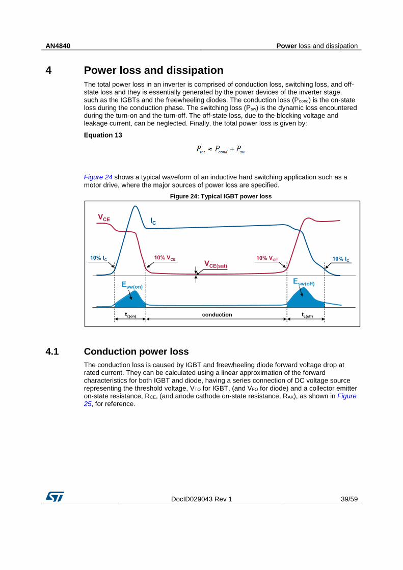
4 Power loss and dissipation
The total power loss in an inverter is comprised of conduction loss, switching loss, and off-state loss and they is essentially generated by the power devices of the inverter stage, such as the IGBTs and the freewheeling diodes. The conduction loss (Pcond) is the on-state loss during the conduction phase. The switching loss (Psw) is the dynamic loss encountered during the turn-on and the turn-off. The off-state loss, due to the blocking voltage and leakage current, can be neglected. Finally, the total power loss is given by:
Equation 13
Figure 24 shows a typical waveform of an inductive hard switching application such as a motor drive, where the major sources of power loss are specified.
Figure 24: Typical IGBT power loss
4.1 Conduction power loss
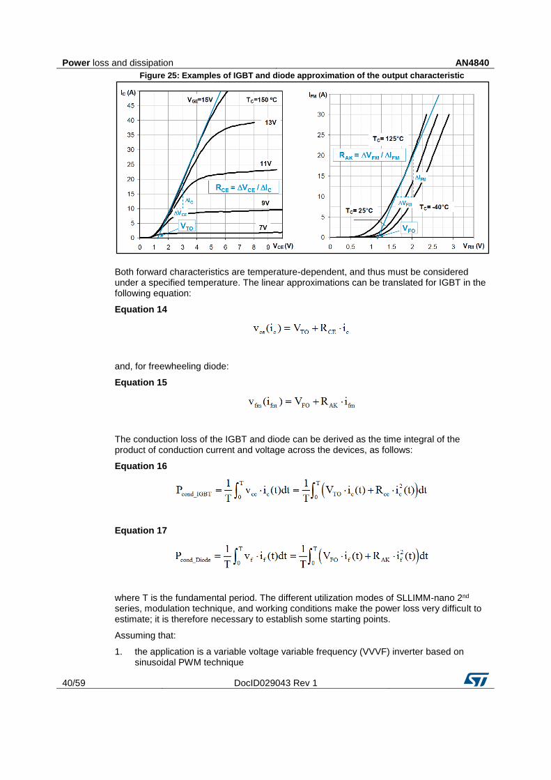
The conduction loss is caused by IGBT and freewheeling diode forward voltage drop at rated current. They can be calculated using a linear approximation of the forward characteristics for both IGBT and diode, having a series connection of DC voltage source representing the threshold voltage, VTO for IGBT, (and VFO for diode) and a collector emitter on-state resistance, RCE, (and anode cathode on-state resistance, RAK), as shown in Figure 25, for reference.
Power loss and dissipation AN4840
40/59 DocID029043 Rev 1
Figure 25: Examples of IGBT and diode approximation of the output characteristic
Both forward characteristics are temperature-dependent, and thus must be considered under a specified temperature. The linear approximations can be translated for IGBT in the following equation:
Equation 14
and, for freewheeling diode:
Equation 15
The conduction loss of the IGBT and diode can be derived as the time integral of the product of conduction current and voltage across the devices, as follows:
Equation 16
Equation 17
where T is the fundamental period. The different utilization modes of SLLIMM-nano 2nd series, modulation technique, and working conditions make the power loss very difficult to estimate; it is therefore necessary to establish some starting points.
Assuming that:
1. the application is a variable voltage variable frequency (VVVF) inverter based on sinusoidal PWM technique

AN4840 Power loss and dissipation
DocID029043 Rev 1 41/59
2. the switching frequency is high and therefore the output currents are sinusoidal 3. the load is ideal inductive
Under these conditions, the output inverter current is given by:
Equation 18
where Î is the current peak, θ stands for ωt and ϕ is the phase angle between output voltage and current.
The conduction power loss can be obtained as:
Equation 19
Equation 20
where ξ is the duty cycle for this PWM technique and is given by:
Equation 21
and ma is the PWM amplitude modulation index.
Finally, solving Equations 19 and 20, we have:
Equation 22
Equation 23
and therefore, the conduction power loss of one device (IGBT and diode) is:
Equation 24
Power loss and dissipation AN4840
42/59 DocID029043 Rev 1
Of course, the total conduction loss per inverter is six times this value.
4.2 Switching power loss
The switching loss is the power consumption during the turn-on and turn-off transients. As shown in Figure 24: "Typical IGBT power loss", it is given by the pulse of power dissipated during the turn-on (ton) and turn-off (toff). Experimentally, it can be calculated by the time integral of the product of the collector current and collector-emitter voltage for the switching period. In any case, the dynamic performances are strictly related to many parameters such as voltage, current and temperature, so it is necessary to use the same conduction power loss assumptions (Section 4.1: "Conduction power loss") to simplify the calculations.
Under these conditions, the switching energy loss is given by:
Equation 25
Equation 26
where Êon and Êoff are the maximum values taken at Tjmax and Îc, θ stands for ωt and ϕ is the phase angle between output voltage and current.
Finally, the switching power loss per device depends on the switching frequency (fsw) and is calculated as follows:
Equation 27
where EIGBT and EDiode are the total switching energy for the IGBT and freewheeling diode, respectively. Also in this case, the total switching loss per inverter is six times this value.
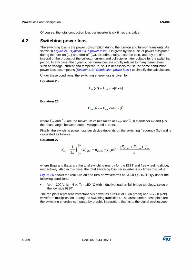
Figure 26 shows the real turn-on and turn-off waveforms of STGIPQ5H60T-Hyy under the following conditions:
VPN = 300 V, IC = 5 A, Tj = 150 °C with inductive load on full bridge topology, taken on the low side IGBT.
The red plots represent instantaneous power as a result of IC (in green) and VCE (in pink) waveform multiplication, during the switching transitions. The areas under these plots are the switching energies computed by graphic integration, thanks to the digital oscilloscope.
AN4840 Power loss and dissipation
DocID029043 Rev 1 43/59
Figure 26: Typical switching waveforms of the STGIPQ5H60T-Hyy
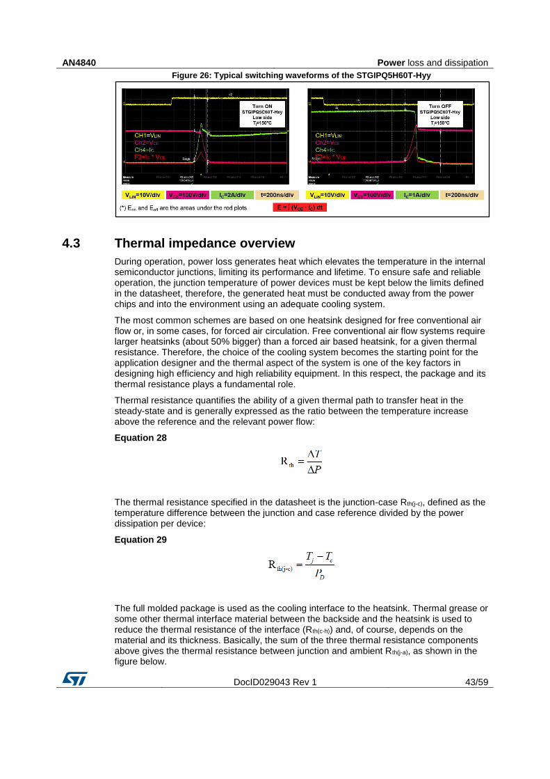
4.3 Thermal impedance overview
During operation, power loss generates heat which elevates the temperature in the internal semiconductor junctions, limiting its performance and lifetime. To ensure safe and reliable operation, the junction temperature of power devices must be kept below the limits defined in the datasheet, therefore, the generated heat must be conducted away from the power chips and into the environment using an adequate cooling system.
The most common schemes are based on one heatsink designed for free conventional air flow or, in some cases, for forced air circulation. Free conventional air flow systems require larger heatsinks (about 50% bigger) than a forced air based heatsink, for a given thermal resistance. Therefore, the choice of the cooling system becomes the starting point for the application designer and the thermal aspect of the system is one of the key factors in designing high efficiency and high reliability equipment. In this respect, the package and its thermal resistance plays a fundamental role.
Thermal resistance quantifies the ability of a given thermal path to transfer heat in the steady-state and is generally expressed as the ratio between the temperature increase above the reference and the relevant power flow:
Equation 28
The thermal resistance specified in the datasheet is the junction-case Rth(j-c), defined as the temperature difference between the junction and case reference divided by the power dissipation per device:
Equation 29
The full molded package is used as the cooling interface to the heatsink. Thermal grease or some other thermal interface material between the backside and the heatsink is used to reduce the thermal resistance of the interface (Rth(c-h)) and, of course, depends on the material and its thickness. Basically, the sum of the three thermal resistance components above gives the thermal resistance between junction and ambient Rth(j-a), as shown in the figure below.
Power loss and dissipation AN4840
44/59 DocID029043 Rev 1
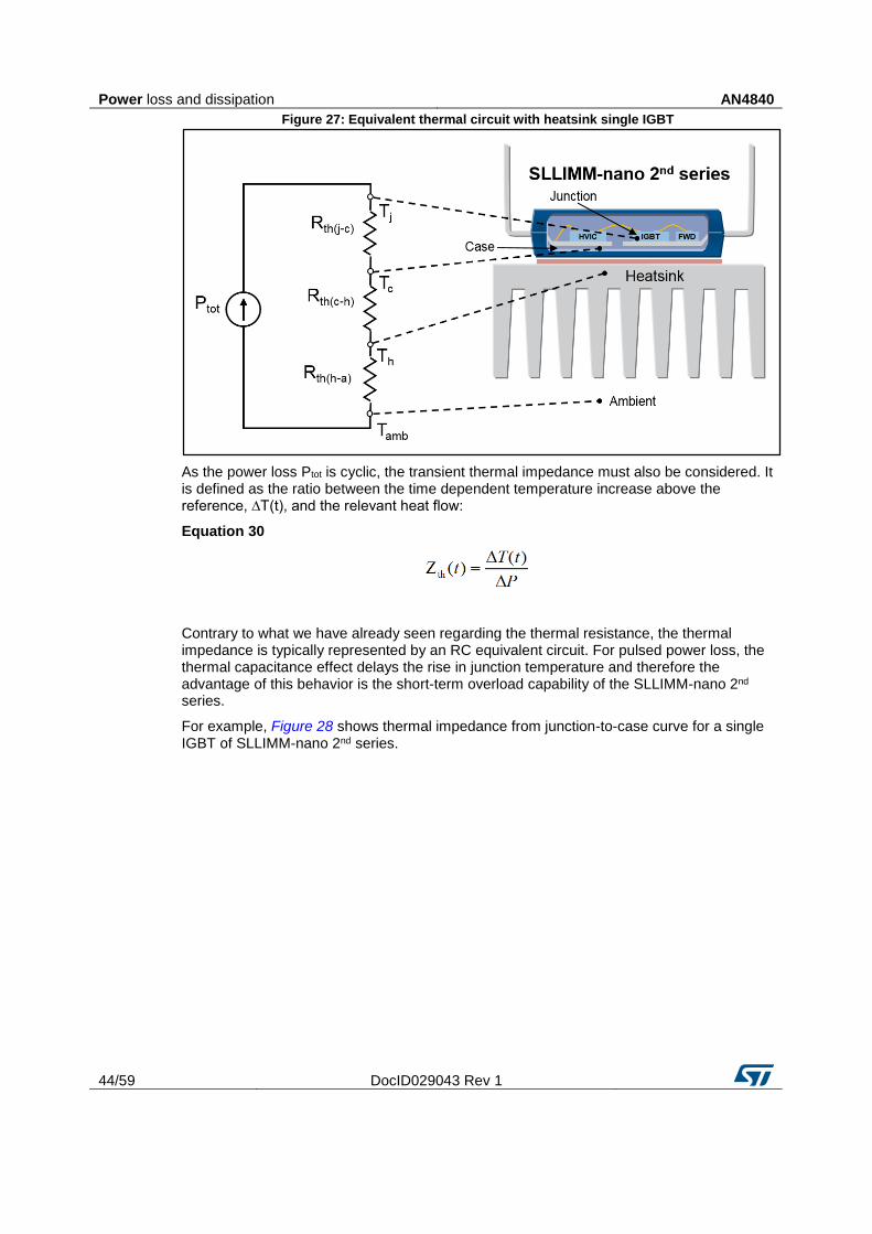
Figure 27: Equivalent thermal circuit with heatsink single IGBT
As the power loss Ptot is cyclic, the transient thermal impedance must also be considered. It is defined as the ratio between the time dependent temperature increase above the reference, ∆T(t), and the relevant heat flow:
Equation 30
Contrary to what we have already seen regarding the thermal resistance, the thermal impedance is typically represented by an RC equivalent circuit. For pulsed power loss, the thermal capacitance effect delays the rise in junction temperature and therefore the advantage of this behavior is the short-term overload capability of the SLLIMM-nano 2nd series.
For example, Figure 28 shows thermal impedance from junction-to-case curve for a single IGBT of SLLIMM-nano 2nd series.
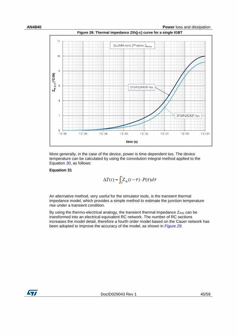
AN4840 Power loss and dissipation
DocID029043 Rev 1 45/59
Figure 28: Thermal impedance Zth(j-c) curve for a single IGBT
More generally, in the case of the device, power is time-dependent too. The device temperature can be calculated by using the convolution integral method applied to the Equation 30, as follows:
Equation 31
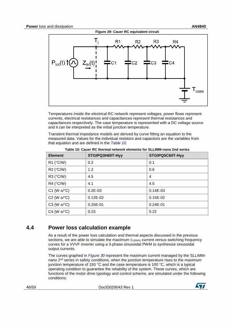
An alternative method, very useful for the simulator tools, is the transient thermal impedance model, which provides a simple method to estimate the junction temperature rise under a transient condition.
By using the thermo-electrical analogy, the transient thermal impedance Zth(t) can be transformed into an electrical equivalent RC network. The number of RC sections increases the model detail, therefore a fourth order model based on the Cauer network has been adopted to improve the accuracy of the model, as shown in Figure 29.
Power loss and dissipation AN4840
46/59 DocID029043 Rev 1
Figure 29: Cauer RC equivalent circuit
Temperatures inside the electrical RC network represent voltages, power flows represent currents, electrical resistances and capacitances represent thermal resistances and capacitances respectively. The case temperature is represented with a DC voltage source and it can be interpreted as the initial junction temperature.
Transient thermal impedance models are derived by curve fitting an equation to the measured data. Values for the individual resistors and capacitors are the variables from that equation and are defined in the Table 10.
Table 10: Cauer RC thermal network elements for SLLIMM-nano 2nd series
Element STGIPQ3H60T-Hyy STGIPQ5C60T-Hyy
R1 (°C/W) 0.2 0.1
R2 (°C/W) 1.2 0.6
R3 (°C/W) 4.5 4
R4 (°C/W) 4.1 4.5
C1 (W·s/°C) 0.2E-03 0.14E-03
C2 (W·s/°C) 0.12E-02 0.15E-02
C3 (W·s/°C) 0.25E-01 0.24E-01
C4 (W·s/°C) 0.23 0.22
4.4 Power loss calculation example
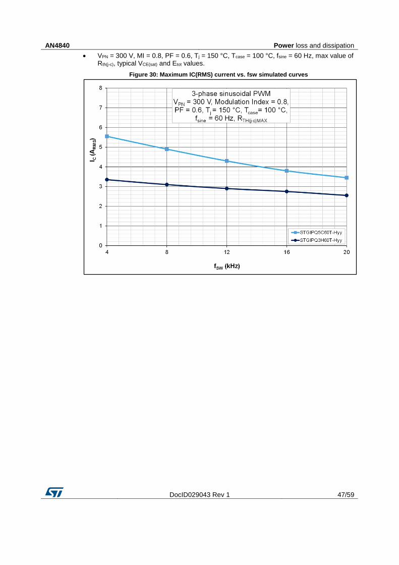
As a result of the power loss calculation and thermal aspects discussed in the previous sections, we are able to simulate the maximum IC(RMS) current versus switching frequency curves for a VVVF inverter using a 3-phase sinusoidal PWM to synthesize sinusoidal output currents.
The curves graphed in Figure 30 represent the maximum current managed by the SLLIMM-nano 2nd series in safety conditions, when the junction temperature rises to the maximum junction temperature of 150 °C and the case temperature is 100 °C, which is a typical operating condition to guarantee the reliability of the system. These curves, which are functions of the motor drive typology and control scheme, are simulated under the following conditions:
AN4840 Power loss and dissipation
DocID029043 Rev 1 47/59
VPN = 300 V, MI = 0.8, PF = 0.6, Tj = 150 °C, Tcase = 100 °C, fsine = 60 Hz, max value of Rth(j-c), typical VCE(sat) and Etot values.
Figure 30: Maximum IC(RMS) current vs. fsw simulated curves

Design and mounting guidelines AN4840
48/59 DocID029043 Rev 1
5 Design and mounting guidelines
In this section the main layout suggestions for an optimized design and major mounting recommendations to appropriately handle and assemble the SLLIMM-nano 2nd series family, will be introduced.
5.1 Typical circuit and recommendations
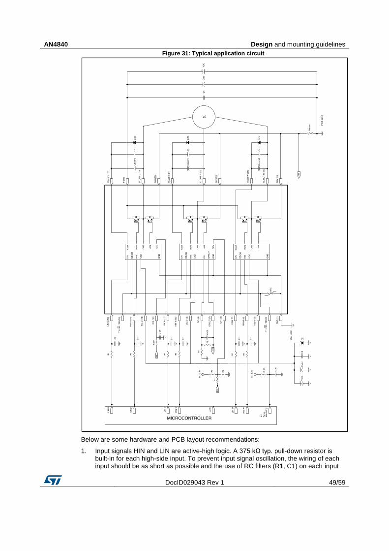
The figure below shows a typical application circuit using the SLLIMM-nano 2nd series, including signal interfaces with the MCU.
AN4840 Design and mounting guidelines
DocID029043 Rev 1 49/59
Figure 31: Typical application circuit
Below are some hardware and PCB layout recommendations:
1. Input signals HIN and LIN are active-high logic. A 375 kΩ typ. pull-down resistor is built-in for each high-side input. To prevent input signal oscillation, the wiring of each input should be as short as possible and the use of RC filters (R1, C1) on each input

Design and mounting guidelines AN4840
50/59 DocID029043 Rev 1
signal is suggested. The filters should be implemented with a time constant of about 100 ns and placed as close as possible to the IPM input pins.
2. Bypass capacitor CVCC (aluminum or tantalum) is recommended to reduce the transient circuit demand on the power supply. In addition, a decoupling capacitor C2 (100 to 220 nF, with low ESR, low ESL) is suggested to reduce high frequency switching noise distributed on the power supply lines. It must be placed as close as possible to the VCC pin and in parallel with the bypass capacitor.
3. The use of the RC filter (RSF, CSF) to help prevent malfunction of the protection circuit is recommended. The time constant (RSF x CSF) should be set to 1 us and the filter placed as close as possible to the CIN pin.
4. The SD pin is an input/output pin (open drain type if used as output). An integrated NTC thermistor is connected internally between the SD pin and GND. The pull-up resistor RSD causes the voltage VSD-GND to decrease as the temperature increases. To always maintain the voltage above the high-level logic threshold, use a 1 kΩ or 2.2 kΩ pull-up resistor for a 3.3 V or 5 V MCU power supply, respectively. Size the filter on SD appropriately to obtain the desired restart time after a fault event, and place it as close as possible to the SD pin.
5. Decoupling capacitor C3 (100 to 220 nF, with low ESR and low ESL) in parallel with each Cboot is recommended in order to filter high frequency disturbances. Both Cboot and C3 must be placed as close as possible to the U, V, W and Vboot pins. Bootstrap negative electrodes should be connected to U, V, W terminals directly and separated from the main output wires.
6. A Zener diode (Dz1) between each VCC pin and GND, and in parallel (Dz2) with each Cboot is suggested in order to prevent overvoltage.
7. Capacitor C4 (100 to 220 nF, low ESR and low ESL) in parallel with the electrolytic capacitor Cvdc is recommended in order to prevent surge destruction. Both capacitors C4 and Cvdc should be placed as close as possible to the IPM (C4 has priority over Cvdc).
8. By integrating an application-specific type HVIC inside the module, direct coupling to the MCU terminals without an optocoupler is possible.
9. Low inductance shunt resistors should be used for phase leg current sensing. 10. In order to avoid malfunction, the wiring between N pins, the shunt resistor and
PWR_GND should be as short as possible. 11. It is recommended to connect SGN_GND to PWR_GND at only one point (near the
shunt resistor terminal), in order to avoid any malfunction due to power ground fluctuation.
5.2 Layout suggestions
PCB layout optimization for high voltage, high current and high switching frequency applications is a critical factor. PCB layout is a complex matter involving several aspects such as track length and width and circuit areas, but also the proper routing of the traces and the optimized reciprocal arrangement of the various system elements in the PCB area.
A good layout can help the application function properly and achieve expected performance. On the other hand, PCBs without careful layout can generate EMI issues (both induced and perceived by the application), can provide overvoltage spikes due to parasitic inductances along the PCB traces, and can produce higher power loss and even malfunction in the control and sensing stages.
The compactness of the SLLIMM-nano 2nd series solution, which offers an optimized gate driving network and reduced parasitic elements, allows designers to concentrate on other issues such as the ground or noise filter. In any case, to avoid the aforementioned conditions, the following general PCB layout guidelines and suggestions should be followed for 3-phase applications.
For more information please refer to application note AN4694.
AN4840 Design and mounting guidelines
DocID029043 Rev 1 51/59
5.2.1 General suggestions
1. PCB traces should be designed as short as possible and the area of the circuit (power or signal) minimized to reduce the sensitivity of such structures to surrounding noise.
2. Ensure a good distance between switching lines with high voltage transitions and the signal lines sensitive to electrical noise. Specifically, the tracks of each OUT phase carrying significant currents and voltages should be separated from logic lines and analog op-amp and comparator sensing circuits.
3. Place the RSENSE resistors as close as possible to the low-side pins of the SLLIMM-nano 2nd series (N U, N V and N W). Parasitic inductance can be minimized by connecting the ground line (also called driver ground) of the SLLIMM-nano 2nd series directly to the cold terminal of sense resistors. Use a low inductance type resistor, such as an SMD resistor instead of long lead type resistors, to help further decrease parasitic inductance.
4. Avoid any ground loop. Only a single path must connect two different ground nodes. 5. Place each RC filter as close as possible to the SLLIMM-nano 2nd series pins in order
to increase their effectiveness. 6. Fixed voltage tracks such as GND or HV lines can be used to shield the logic and
analog lines from electrical noise produced by the switching lines (e.g., OUT U, OUT V and OUT W).
7. Generally, it is recommended to connect each half bridge ground in a star configuration and the three RSENSE very close to each other and to the power ground.
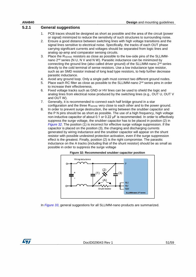
8. In order to prevent surge destruction, the wiring between the snubber capacitor and the P N pins should be as short as possible. The use of a high frequency, high voltage non-inductive capacitor of about 0.1 or 0.22 μF is recommended. In order to effectively suppress the surge voltage, the snubber capacitor has to be placed in position (2) in Figure 32. The position (1) is incorrect for effective surge voltage suppression. If the capacitor is placed on the position (3), the charging and discharging currents generated by wiring inductance and the snubber capacitor will appear on the shunt resistor with possible undesired protection activation, even if the surge suppression effect is the greatest. Finally, position (2) is the right compromise. The parasitic inductance on the A tracks (including that of the shunt resistor) should be as small as possible in order to suppress the surge voltage
Figure 32: Recommended snubber capacitor position
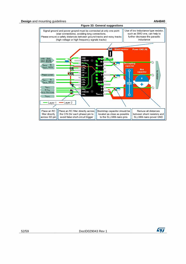
In Figure 33, general suggestions for all SLLIMM-nano products are summarized.
Design and mounting guidelines AN4840
52/59 DocID029043 Rev 1
Figure 33: General suggestions

AN4840 Mounting and handling instructions
DocID029043 Rev 1 53/59
6 Mounting and handling instructions
Some basic assembly rules must be followed in order to limit thermal and mechanical stress and optimize the thermal conduction and electrical isolation for the N2DIP package when mounting a heatsink.
Moreover, semiconductors are normally electrostatic discharge sensitive devices (ESDS) requiring specific precautionary measures regarding handling and processing. Static discharges caused by human touch or by processing tools may cause high-current and/or high-voltage pulses which may damage or even destroy sensitive semiconductor structures. Integrated circuits (ICs) may also be charged by static during processing. If discharging takes place too quickly (“hard” discharge), it may cause peak loads and consequent damage.
Make careful choices regarding workspaces, personal equipment and processing and assembly equipment.
6.1 Heatsink mounting
When attaching a heatsink to a SLLIMM-nano 2nd series, do not apply excessive force to the device for assembly. Drill holes for screws in the heatsink exactly as specified. Smooth the surface by removing burrs and protrusions. Do not touch the heatsink when the SLLIMM-nano 2nd series is operational to avoid burn injury.
To get the most effective heat dissipation, enlarge the contact area as much as possible to minimize the contact thermal resistance. Properly apply thermal-conductive grease over the contact surface between modules and heatsinks, is also useful for preventing contact surfaces from corrosion. Apply a minimum 150 μm layer of thermal grease to the module base plate or to the heatsink, as shown in the figure below. Use a torque screwdriver to fasten to the max specified torque rating. Exceeding the maximum torque may lead to module damage or degradation.
Remove any dirt from the contact surface.
Ensure the grease quality remains constant over time and is able to perform long-term over a wide operating temperature range.
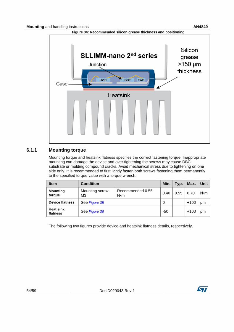
Mounting and handling instructions AN4840
54/59 DocID029043 Rev 1
Figure 34: Recommended silicon grease thickness and positioning
6.1.1 Mounting torque
Mounting torque and heatsink flatness specifies the correct fastening torque. Inappropriate mounting can damage the device and over tightening the screws may cause DBC substrate or molding compound cracks. Avoid mechanical stress due to tightening on one side only. It is recommended to first lightly fasten both screws fastening them permanently to the specified torque value with a torque wrench.
Item Condition Min. Typ. Max. Unit
Mounting torque
Mounting screw: M3
Recommended 0.55 N•m
0.40 0.55 0.70 N•m
Device flatness See Figure 35 0
+100 μm
Heat sink flatness
See Figure 36 -50
+100 μm
The following two figures provide device and heatsink flatness details, respectively.
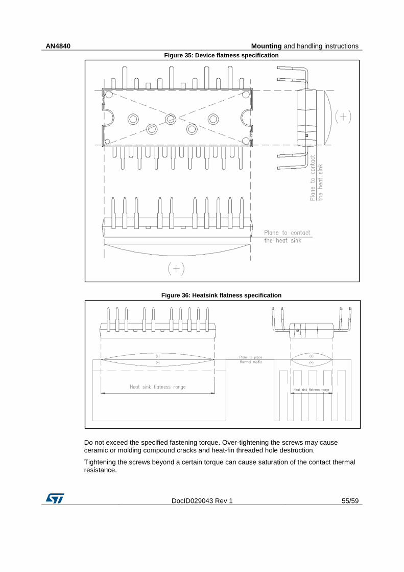
AN4840 Mounting and handling instructions
DocID029043 Rev 1 55/59
Figure 35: Device flatness specification
Figure 36: Heatsink flatness specification
Do not exceed the specified fastening torque. Over-tightening the screws may cause ceramic or molding compound cracks and heat-fin threaded hole destruction.
Tightening the screws beyond a certain torque can cause saturation of the contact thermal resistance.
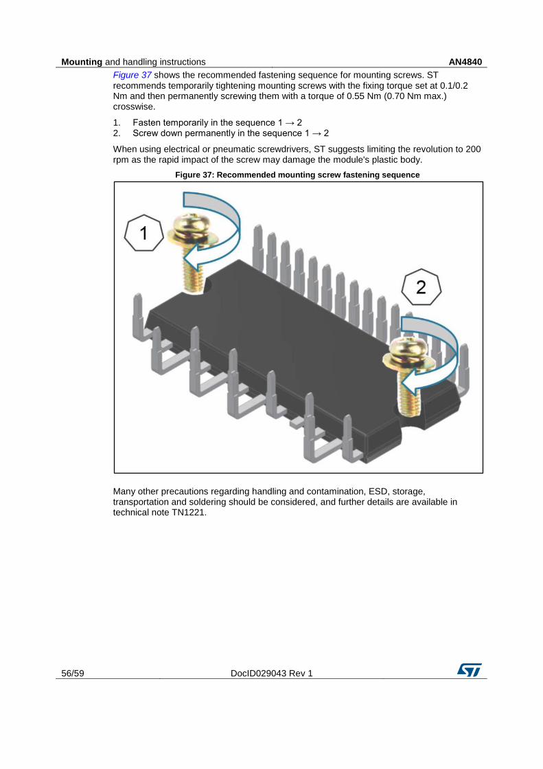
Mounting and handling instructions AN4840
56/59 DocID029043 Rev 1
Figure 37 shows the recommended fastening sequence for mounting screws. ST recommends temporarily tightening mounting screws with the fixing torque set at 0.1/0.2 Nm and then permanently screwing them with a torque of 0.55 Nm (0.70 Nm max.) crosswise.
1. Fasten temporarily in the sequence 1 → 2 2. Screw down permanently in the sequence 1 → 2
When using electrical or pneumatic screwdrivers, ST suggests limiting the revolution to 200 rpm as the rapid impact of the screw may damage the module's plastic body.
Figure 37: Recommended mounting screw fastening sequence
Many other precautions regarding handling and contamination, ESD, storage, transportation and soldering should be considered, and further details are available in technical note TN1221.

AN4840 References
DocID029043 Rev 1 57/59
7 References
1. STGIPQ3H60T-Hyy datasheet 2. STGIPQ5C60T-Hyy datasheet 3. AN4043 – “SLLIMM™-nano” 4. AN4694 – “EMC design guides for motor control applications” 5. TN1221 – “Mounting instruction for SLLIMM™-nano 2nd series”

Revision history AN4840
58/59 DocID029043 Rev 1
8 Revision history Table 11: Document revision history
Date Version Changes
01-Jul-2016 1 Initial release.

AN4840
DocID029043 Rev 1 59/59
IMPORTANT NOTICE – PLEASE READ CAREFULLY
STMicroelectronics NV and its subsidiaries (“ST”) reserve the right to make changes, corrections, enhancements, modifications , and improvements to ST products and/or to this document at any time without notice. Purchasers should obtain the latest relevant information on ST products before placing orders. ST products are sold pursuant to ST’s terms and conditions of sale in place at the time of order acknowledgement.
Purchasers are solely responsible for the choice, selection, and use of ST products and ST assumes no liability for application assistance or the design of Purchasers’ products.
No license, express or implied, to any intellectual property right is granted by ST herein.
Resale of ST products with provisions different from the information set forth herein shall void any warranty granted by ST for such product.
ST and the ST logo are trademarks of ST. All other product or service names are the property of their respective owners.
Information in this document supersedes and replaces information previously supplied in any prior versions of this document.
© 2016 STMicroelectronics – All rights reserved


![[12 0210] gpg 2.3.7 전략적 판단 기법](https://img.pdfslide.net/doc/110x75/549a489aac7959132e8b5b54/12-0210-gpg-237-.jpg)