Embed Size (px)
Citation preview

by: NXP Semiconductors
1 IntroductionThis application note explains how to use the MPC574xG and MPC574xC clock calculators, which are interactive, graphical tools that help customers quickly calculate clock domain frequencies for the respective production families. NXP offers two solution sets for automotive/industrial control and gateway applications: the MPC574xG family, a comprehensive and fully-equipped MCU; and the MPC574xC family, a lower-cost subset for simpler gateway applications. The MPC574xC is structurally identical to the MPC574xG, but sheds some peripheral instances. For example, the MPC574xG supports six SPIs and two main cores, but the MPC574xC supports four SPIs and one main core. These reductions are intended for customers who do not need the comprehensive feature set of the MPC574xG, but still require an MCU for their applications. These two tools cover the MPC574xG and MPC574xC families, respectively.
Despite being structurally identical, there are slight differences between these two product families in the clock selection of some clock domains, which warrants a separate tool for each family. Aside from the differences mentioned above, the MPC574xG and MPC574xC clock calculators are virtually identical. For each derivative within the family, simply ignore the modules in the associated clock calculator that do not exist in the derivative device. Therefore, for brevity, the rest of this application note refers to all devices in the MPC574xG and MPC574xC families as simply “MPC5748G” and the figures that appear are exclusively from the MPC574xG clock calculator.
The MPC5748G is the company’s next-generation integrated solution forsecure central body control, gateway, and industrial applications. It is built uponup to two 32-bit e200z4 cores, running up to 160 MHz, and one 32-bit e200z2core, running up to 80 MHz. This device supports four clock oscillators and one Frequency-Modulated Phase Locked Loop(FMPLL) for a total of five clock sources. Of the four oscillators, there is an 8-40 MHz Fast External Oscillator (FXOSC), a 16MHz Fast Internal RC Oscillator (FIRC), a 32 kHz Slow External Oscillator (SXOSC), and a 128 kHz slow internal RC Oscillator(SIRC). The FMPLL multiplies one of these four sources and produces two outputs, each of which can go up to 160 MHz. TheMPC574xG clock calculator is meant to be a complement to MPC574xG reference manual. It seeks to simplify the clockconfiguration process by providing a graphical, interactive tool to help the user find the correct register settings in order to achievehis/her desired clock frequencies.
Accompanying this application note are the clock calculators themselves. You can download them from MPC574xC andMPC574xG clock calculator.
The clock calculator makes use of macros to perform functions like resetting the spreadsheet to initial values, configuring all clockfrequencies to the maximum allowable settings, and copying generated code. Macros must be enabled in the user's MS Excelto access these features. If macros are turned off however, the tool will still be able to calculate clock frequencies, but theaforementioned features will be disabled. To turn on macros in MS Excel 2016, go to the Developer on the top toolbar and clickon Macro Security. A popup window will appear. In it, select Enable all macros.
Contents
1 Introduction............................................ 1
2 Clock calculator design..........................22.1 Tree.............................. 32.2 Clock Source Control....62.3 Module domains........... 72.4 ENET Clocking/SAI
Clocking......................... 82.5 CAN Clocking............... 92.6 FMPLL........................ 102.7 Reference tables
(FMPLL_PHI0 andFMPLL_PHI1).............. 11
2.8 Summary.................... 112.9 Limits.......................... 14
3 Clock tool example use case:Configure FlexCAN to FMPLL at40 MHz and FS80 at 80 MHz in runmode................................................. 16
3.1 Configure FS80.......... 163.2 Configure F40.............263.3 Configure FlexCAN
Clocks.......................... 273.4 Observe the registers. 273.5 Copy the code............ 28
4 Conclusion........................................... 29
5 Revision history................................... 30
AN5392MPC574xG/MPC574xC Clock Calculator GuideHow to use MPC5748G tool to easily calculate device frequency domainsRev. 5 — June 2020 Application Note
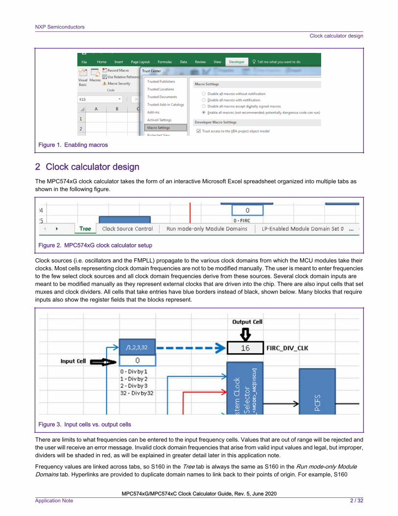
Figure 1. Enabling macros
2 Clock calculator designThe MPC574xG clock calculator takes the form of an interactive Microsoft Excel spreadsheet organized into multiple tabs asshown in the following figure.
Figure 2. MPC574xG clock calculator setup
Clock sources (i.e. oscillators and the FMPLL) propagate to the various clock domains from which the MCU modules take theirclocks. Most cells representing clock domain frequencies are not to be modified manually. The user is meant to enter frequenciesto the few select clock sources and all clock domain frequencies derive from these sources. Several clock domain inputs aremeant to be modified manually as they represent external clocks that are driven into the chip. There are also input cells that setmuxes and clock dividers. All cells that take entries have blue borders instead of black, shown below. Many blocks that requireinputs also show the register fields that the blocks represent.
Figure 3. Input cells vs. output cells
There are limits to what frequencies can be entered to the input frequency cells. Values that are out of range will be rejected andthe user will receive an error message. Invalid clock domain frequencies that arise from valid input values and legal, but improper,dividers will be shaded in red, as will be explained in greater detail later in this application note.
Frequency values are linked across tabs, so S160 in the Tree tab is always the same as S160 in the Run mode-only ModuleDomains tab. Hyperlinks are provided to duplicate domain names to link back to their points of origin. For example, S160
NXP SemiconductorsClock calculator design
MPC574xG/MPC574xC Clock Calculator Guide, Rev. 5, June 2020Application Note 2 / 32

originates in Tree. Therefore, clicking the S160 textbox in Run mode-only Module Domains takes the user to S160 in Tree.Textboxes that are links, when hovered over, will cause the mouse cursor to turn into a hand icon and a pop-up to appear, showingthe address of the destination, as shown in the following figure.
Figure 4. Clicking on a link
The following subsections will explain in depth the purpose of each tab.
2.1 TreeTree is the centerpiece of the tool. This tab is the starting point for all clock frequency calculations. It is organized to resemblethe MPC5748G clock tree, as presented in the following figure.
NXP SemiconductorsClock calculator design
MPC574xG/MPC574xC Clock Calculator Guide, Rev. 5, June 2020Application Note 3 / 32
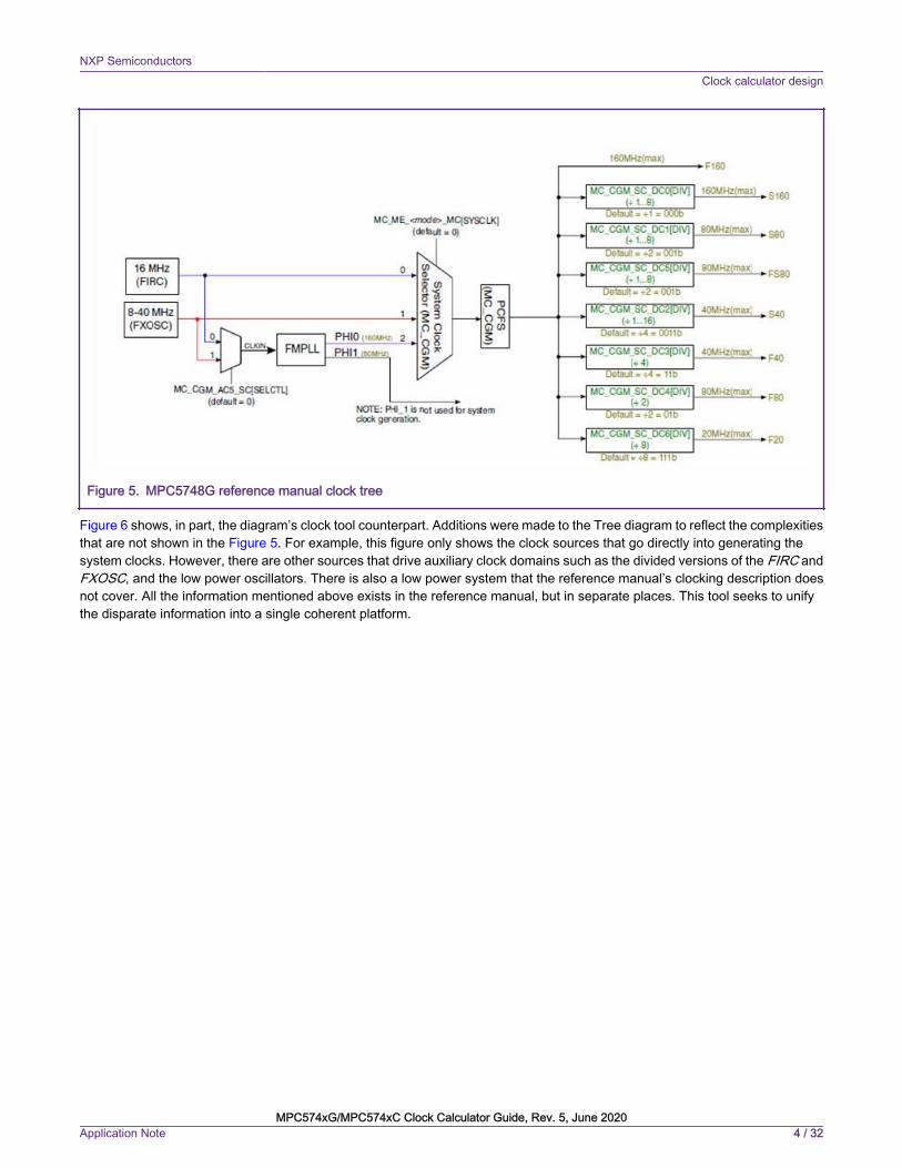
Figure 5. MPC5748G reference manual clock tree
Figure 6 shows, in part, the diagram’s clock tool counterpart. Additions were made to the Tree diagram to reflect the complexitiesthat are not shown in the Figure 5. For example, this figure only shows the clock sources that go directly into generating thesystem clocks. However, there are other sources that drive auxiliary clock domains such as the divided versions of the FIRC andFXOSC, and the low power oscillators. There is also a low power system that the reference manual’s clocking description doesnot cover. All the information mentioned above exists in the reference manual, but in separate places. This tool seeks to unifythe disparate information into a single coherent platform.
NXP SemiconductorsClock calculator design
MPC574xG/MPC574xC Clock Calculator Guide, Rev. 5, June 2020Application Note 4 / 32
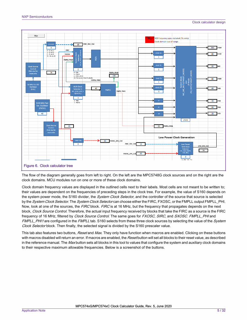
Figure 6. Clock calculator tree
The flow of the diagram generally goes from left to right. On the left are the MPC5748G clock sources and on the right are theclock domains. MCU modules run on one or more of these clock domains.
Clock domain frequency values are displayed in the outlined cells next to their labels. Most cells are not meant to be written to;their values are dependent on the frequencies of preceding steps in the clock tree. For example, the value of S160 depends onthe system power mode, the S160 divider, the System Clock Selector, and the controller of the source that source is selectedby the System Clock Selector. The System Clock Selector can choose either the FIRC, FXOSC, or the FMPLL output FMPLL_PHI.Now, look at one of the sources, the FIRC block. FIRC is at 16 MHz, but the frequency that propagates depends on the nextblock, Clock Source Control. Therefore, the actual input frequency received by blocks that take the FIRC as a source is the FIRCfrequency of 16 MHz, filtered by Clock Source Control. The same goes for FXOSC, SIRC, and SXOSC. FMPLL_PHI andFMPLL_PHI1 are configured in the FMPLL tab. S160 selects from these three clock sources by selecting the value of the SystemClock Selector block. Then finally, the selected signal is divided by the S160 prescaler value.
This tab also features two buttons, Reset and Max. They only have function when macros are enabled. Clicking on these buttonswith macros disabled will return an error. If macros are enabled, the Reset button will set all blocks to their reset value, as describedin the reference manual. The Max button sets all blocks in this tool to values that configure the system and auxiliary clock domainsto their respective maximum allowable frequencies. Below is a screenshot of the buttons.
NXP SemiconductorsClock calculator design
MPC574xG/MPC574xC Clock Calculator Guide, Rev. 5, June 2020Application Note 5 / 32
Figure 7. Buttons
2.2 Clock Source ControlThe MPC5748G’s oscillators can be turned on/off. This feature is reflected in the MPC574xG clock calculator in the Clock SourceControl tab. Each oscillator originates in the Tree tab, but then each signal is filtered through a Clock Source Control block. TheClock Source Control block is a hyperlink to the Clock Source Control tab, where each oscillator can be turned on/off for eachpower mode. A screenshot for Clock Source Control is shown in the figure below.
NXP SemiconductorsClock calculator design
MPC574xG/MPC574xC Clock Calculator Guide, Rev. 5, June 2020Application Note 6 / 32

Figure 8. Clock Source Control
2.3 Module domainsThe module domain tabs are an in-depth explanation of MPC5748G modules. Where Tree leaves off at the clock domain level,the module domain tabs pick up and progress to the module level. This tool splits the modules into three tabs because there arethree power domains in the MPC5748G. Every module belongs to one of them. Run mode-only Module Domains covers modulesthat belong to what is called Power Domain 2 (PD2) in the MPC5748G reference manual. These modules are only enabled infull power modes. This characteristic is reflected in the tool by setting all frequencies in the Run mode-only Module Domains tabto 0 when a low power mode is selected in Tree. Power mode is controlled in this tool by selecting the value of the System Modeblock in Tree. LP-Enabled Module Domain Set 1 contains modules that belong to PD1, as it is called in the reference manual.These modules are enabled in all modes except LPU_STANDBY and LPU_STOP. Finally, LP-Enabled Module Domain Set 0consists of modules that belong to PD0, which are powered throughout all modes. Modules that belong to this domain are thosethat are responsible for the barebones operation of the MPC5748G. A screenshot of Run mode-only Module Domains is shownin the figure below.
NXP SemiconductorsClock calculator design
MPC574xG/MPC574xC Clock Calculator Guide, Rev. 5, June 2020Application Note 7 / 32

Figure 9. One of the module domains
The clock domains are color-coded. Black lines are reserved for local clock nodes. For example, FS80 branches out to ADC1,but is filtered through an ADC1 Enable and an ADC1 Clock Select block. The arrow color after the blocks is changed to black todenote that the frequency value associated with that black line applies only to ADC1. As a rule of thumb, clock domains arerepresented with black lines if all modules using it can fit within a single window without having to scroll.
2.4 ENET Clocking/SAI ClockingENET and SAI clock generation feature many more options than other modules, so that they cannot fit into a single block in themodule domain tabs. Therefore, the ENET and SAI blocks in the Run mode-only Module Domains tab are hyperlinks to the ENETclocking and SAI clocking tabs, respectively. The following figure is a screenshot of ENET clocking.
NXP SemiconductorsClock calculator design
MPC574xG/MPC574xC Clock Calculator Guide, Rev. 5, June 2020Application Note 8 / 32
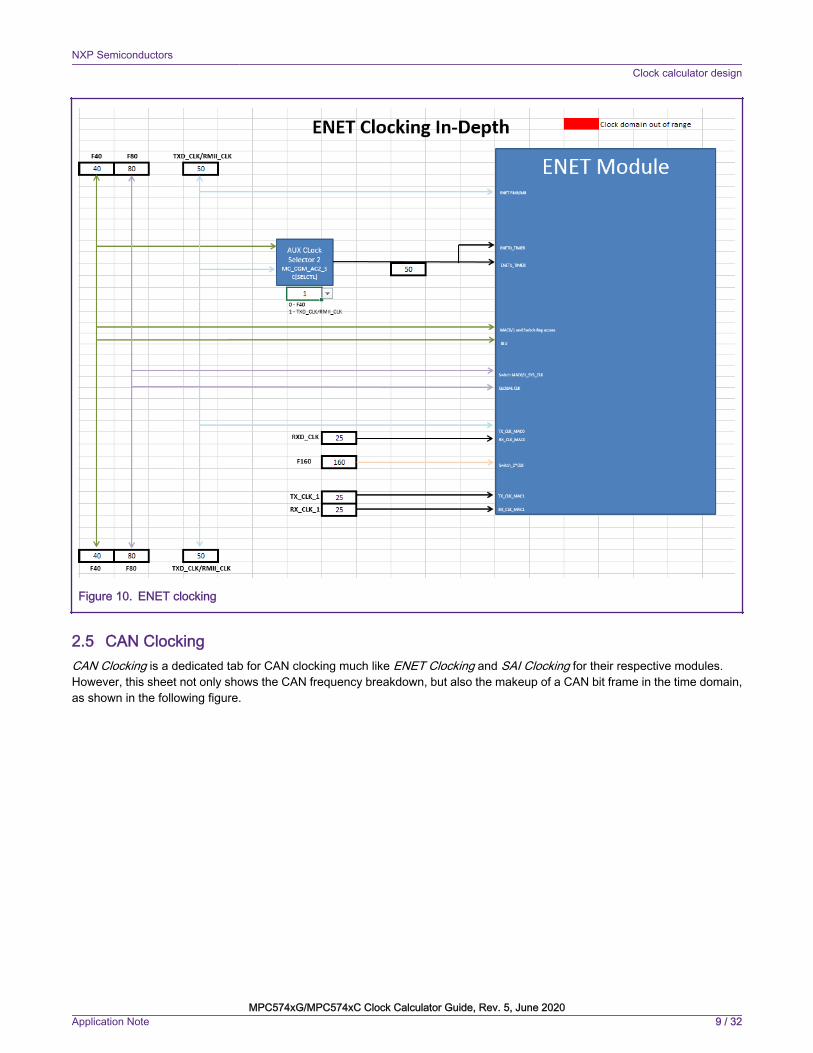
Figure 10. ENET clocking
2.5 CAN ClockingCAN Clocking is a dedicated tab for CAN clocking much like ENET Clocking and SAI Clocking for their respective modules.However, this sheet not only shows the CAN frequency breakdown, but also the makeup of a CAN bit frame in the time domain,as shown in the following figure.
NXP SemiconductorsClock calculator design
MPC574xG/MPC574xC Clock Calculator Guide, Rev. 5, June 2020Application Note 9 / 32
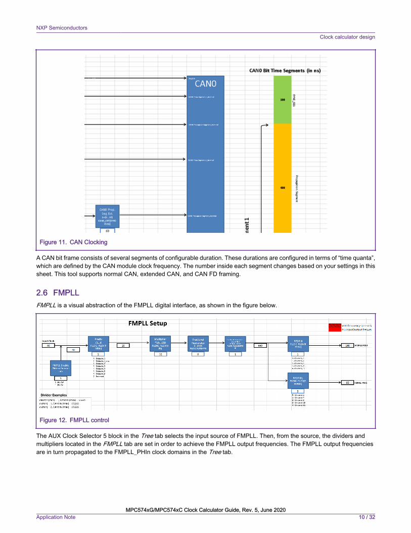
Figure 11. CAN Clocking
A CAN bit frame consists of several segments of configurable duration. These durations are configured in terms of “time quanta”,which are defined by the CAN module clock frequency. The number inside each segment changes based on your settings in thissheet. This tool supports normal CAN, extended CAN, and CAN FD framing.
2.6 FMPLLFMPLL is a visual abstraction of the FMPLL digital interface, as shown in the figure below.
Figure 12. FMPLL control
The AUX Clock Selector 5 block in the Tree tab selects the input source of FMPLL. Then, from the source, the dividers andmultipliers located in the FMPLL tab are set in order to achieve the FMPLL output frequencies. The FMPLL output frequenciesare in turn propagated to the FMPLL_PHIn clock domains in the Tree tab.
NXP SemiconductorsClock calculator design
MPC574xG/MPC574xC Clock Calculator Guide, Rev. 5, June 2020Application Note 10 / 32

2.7 Reference tables (FMPLL_PHI0 and FMPLL_PHI1)The two tabs FMPLL_PHI0 and FMPLL_PHI1 are reference tables for the user to find the appropriate FMPLL dividers andmultipliers to achieve the desired FMPLL frequency. There is a tab for each FMPLL output because the range of acceptabledivider/multiplier values differ between the two. However, they all follow the same setup. Note that Columns A, B, and C of thesetabs are frozen so if the table looks cut off, just scroll left or right.
FMPLL frequencies are calculated from a reference frequency, a reference divider (RFD), a multiplier (MFD), and a prescaler(PREDIV). The FMPLL reference is not manually configurable because there are a finite number of input values the FMPLL cantake. FMPLL can only reference either the 16 MHz FIRC or the 8-40 MHz FXOSC. The FMPLL reference therefore comes fromthe Tree tab. Configure AUX Clock Selector 5 in Tree to select the FMPLL input. Once the FMPLL reference frequency is selected,enter the desired FMPLL output frequency and PREDIV value. The reference table then calculates the output frequency for eachvalid MFD and RFD setting. Like in the other sections, frequencies are color-coded to define which values are valid and whichare not. Shading changes automatically once the output FMPLL frequencies are calculated. MFD and RFD settings that achievethe exact desired frequency are shaded in green; values that exceed the desired frequency, but are within MPC5748G hardwarespecifications are marked in yellow; and frequencies that exceed the MPC5748G hardware specification are colored red. Thefollowing figure is a screenshot of the reference table for FMPLL_PHI1.
Figure 13. FMPLL_PHI1 reference table
2.8 SummaryAlmost all blocks populating this clock calculator represent real register fields in silicon. The Summary tab collates all theinformation from the rest of the clock calculator into a list of register values, a screenshot of which is shown in the following figure.The values in the register summary are interactive, updating automatically when the associated block is changed. Registerslisted within Summary are only the ones whose values are affected by clock configuration, not every single register available inthe SoC.
NXP SemiconductorsClock calculator design
MPC574xG/MPC574xC Clock Calculator Guide, Rev. 5, June 2020Application Note 11 / 32

Figure 14. Register summary table
The register values are displayed in either hexadecimal or binary format, where an “0x” prefix represents hexadecimal and “0b”denotes binary. A capital “X” represents a “don’t care” bit/half-byte. These bits do not affect the clock frequency so users can setthese values to the values that suit their purposes. Users can best utilize Summary by setting the configuration they want in theclock calculator and then copying the resulting register value into code. For example, taking from the figure above, the registerMC_ME_DRUN_MC should be set to 0xX01X0072. Assuming the “X” are “0”, the resulting S32DS C code would be:MC_ME.DRUN_MC.R = 0x00100072;.
Summary also includes an overview of the clock domain frequencies. Since this tool consists of multiple interdependentspreadsheets, it might be cumbersome for users to weave through them all to find a clock domain. This table provides a placewhere all of them can be found. The table is organized by module, followed by the clock type (i.e. BIU clock, peripheral clock,protocol clock, etc.), and finally the frequency, as currently configured. Below is a screenshot.
NXP SemiconductorsClock calculator design
MPC574xG/MPC574xC Clock Calculator Guide, Rev. 5, June 2020Application Note 12 / 32
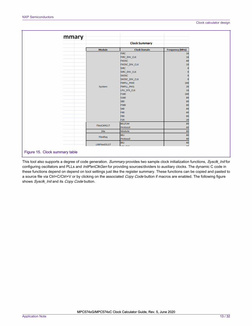
Figure 15. Clock summary table
This tool also supports a degree of code generation. Summary provides two sample clock initialization functions, Sysclk_Init forconfiguring oscillators and PLLs and InitPeriClkGen for providing sources/dividers to auxiliary clocks. The dynamic C code inthese functions depend on depend on tool settings just like the register summary. These functions can be copied and pasted toa source file via Ctrl+C/Ctrl+V or by clicking on the associated Copy Code button if macros are enabled. The following figureshows Sysclk_Init and its Copy Code button.
NXP SemiconductorsClock calculator design
MPC574xG/MPC574xC Clock Calculator Guide, Rev. 5, June 2020Application Note 13 / 32

Figure 16. Sample initialization code
2.9 LimitsLimits is the reference tab for all the color-coding rules. It also contains the reset and maximum values that the Reset and Maxbuttons use. The values in its tables are based on the MPC5748G’s datasheet and reference manual and so should not bemodified by the user. The following figure is a screenshot of the Limits tab.
NXP SemiconductorsClock calculator design
MPC574xG/MPC574xC Clock Calculator Guide, Rev. 5, June 2020Application Note 14 / 32

Figure 17. MPC5748G frequency limits
NXP SemiconductorsClock calculator design
MPC574xG/MPC574xC Clock Calculator Guide, Rev. 5, June 2020Application Note 15 / 32

3 Clock tool example use case: Configure FlexCAN to FMPLL at 40 MHz andFS80 at 80 MHz in run mode
The following section and subsections will present an example application of the MPC574xG clock calculator. This applicationnote’s example configures the FlexCAN to FMPLL at 40 MHz and does not only show the correct configurations, but also howthe tool responds if improper configurations are attempted.
When configuring clocks for a module, start by looking at the module block. For this example, find FlexCAN1:7 within Run mode-only Module Domains.
Figure 18. FlexCAN clocks
The module diagram shows that FS80 drives the bus interface and either FXOSC or F40 drives the FlexCAN protocol engineclock. FS80 and FXOSC are currently at 8 MHz and 0 MHz, respectively. Configuring the clock calculator can be in any order;this example will start with FS80.
3.1 Configure FS80Click on FS80; it will take you to the FS80 of Tree, shown in the figure below.
NXP SemiconductorsClock tool example use case: Configure FlexCAN to FMPLL at 40 MHz and FS80 at 80 MHz in run mode
MPC574xG/MPC574xC Clock Calculator Guide, Rev. 5, June 2020Application Note 16 / 32

Figure 19. FS80, Tree tab
Trace FS80 all the way back to its point of origin. Start by tracing it to the System Mode block, then the FS80 divider, and onwardto the PCFS and System Clock Selector, whose current value is 0. The cell is a drop-down menu and the textbox explains whateach available value is associated with.
Since the only way to achieve 80 MHz is through the FMPLL, trace FMPLL_PHI0 back to its own sources. FMPLL selects fromeither the FIRC or FXOSC via AUX Clock Selector 5. These oscillators are the point of origin for all clock domains. The figurebelow shows FS80 being traced back to the oscillators. It also shows that in the current configuration, the system is in Run modeand FS80 is sourced from the 16MHz FIRC, divided by 2, for a final frequency of 8 MHz.
NXP SemiconductorsClock tool example use case: Configure FlexCAN to FMPLL at 40 MHz and FS80 at 80 MHz in run mode
MPC574xG/MPC574xC Clock Calculator Guide, Rev. 5, June 2020Application Note 17 / 32
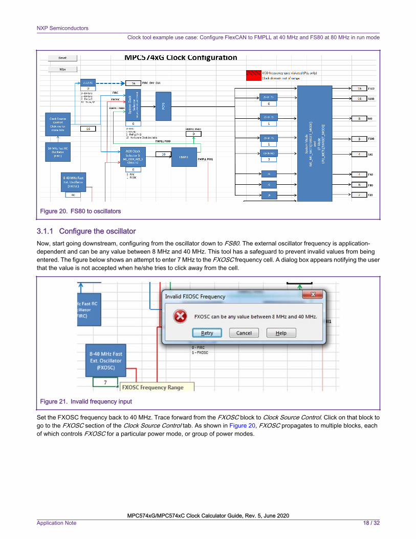
Figure 20. FS80 to oscillators
3.1.1 Configure the oscillatorNow, start going downstream, configuring from the oscillator down to FS80. The external oscillator frequency is application-dependent and can be any value between 8 MHz and 40 MHz. This tool has a safeguard to prevent invalid values from beingentered. The figure below shows an attempt to enter 7 MHz to the FXOSC frequency cell. A dialog box appears notifying the userthat the value is not accepted when he/she tries to click away from the cell.
Figure 21. Invalid frequency input
Set the FXOSC frequency back to 40 MHz. Trace forward from the FXOSC block to Clock Source Control. Click on that block togo to the FXOSC section of the Clock Source Control tab. As shown in Figure 20, FXOSC propagates to multiple blocks, eachof which controls FXOSC for a particular power mode, or group of power modes.
NXP SemiconductorsClock tool example use case: Configure FlexCAN to FMPLL at 40 MHz and FS80 at 80 MHz in run mode
MPC574xG/MPC574xC Clock Calculator Guide, Rev. 5, June 2020Application Note 18 / 32

Figure 22. FXOSC control
The system is in DRUN mode, so DRUN Control is the block of concern. Its value is 0, meaning the FXOSC is gated in run mode.For that reason, FXOSC frequencies downstream show 0 MHz. The following figure circles the blocks that represent the FXOSCcrystal and the effective frequency as sensed by AUX Clock Selector 5.
Figure 23. Actual FXOSC frequency with source turned off
Turn on the FXOSC by switching the value of DRUN Control in Clock Source Control to 1. The output FXOSC frequency is now40 MHz, as shown in figure below.
NXP SemiconductorsClock tool example use case: Configure FlexCAN to FMPLL at 40 MHz and FS80 at 80 MHz in run mode
MPC574xG/MPC574xC Clock Calculator Guide, Rev. 5, June 2020Application Note 19 / 32
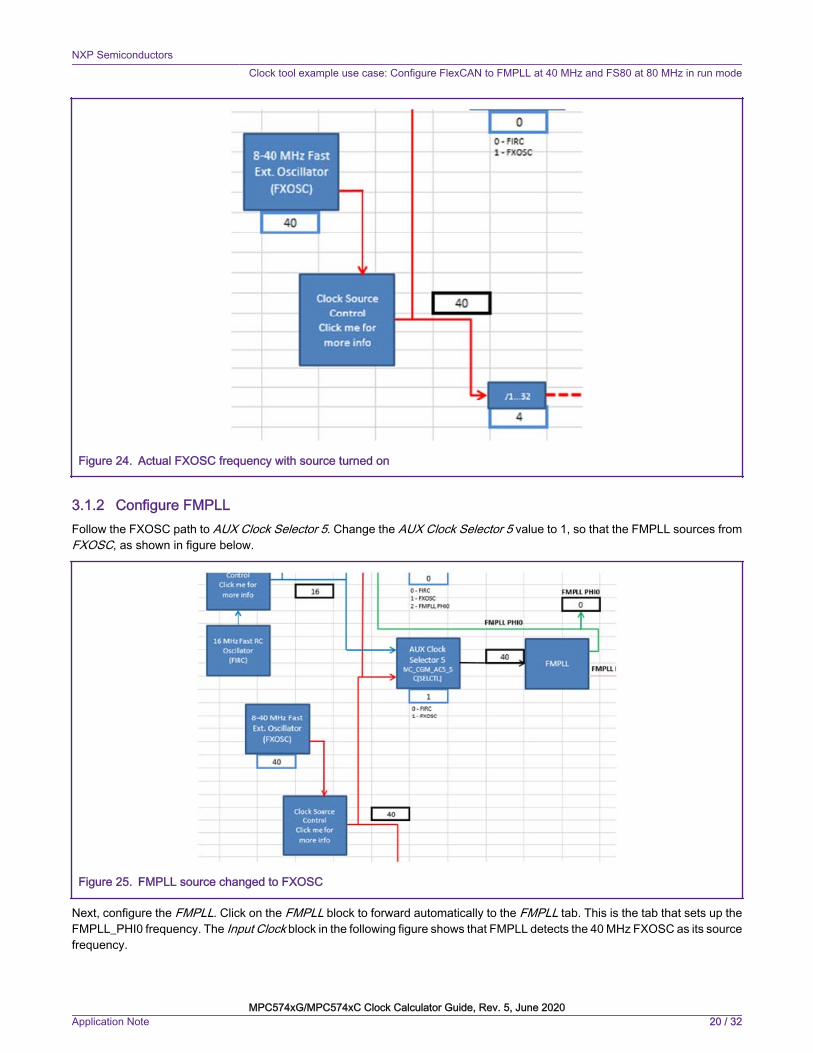
Figure 24. Actual FXOSC frequency with source turned on
3.1.2 Configure FMPLLFollow the FXOSC path to AUX Clock Selector 5. Change the AUX Clock Selector 5 value to 1, so that the FMPLL sources fromFXOSC, as shown in figure below.
Figure 25. FMPLL source changed to FXOSC
Next, configure the FMPLL. Click on the FMPLL block to forward automatically to the FMPLL tab. This is the tab that sets up theFMPLL_PHI0 frequency. The Input Clock block in the following figure shows that FMPLL detects the 40 MHz FXOSC as its sourcefrequency.
NXP SemiconductorsClock tool example use case: Configure FlexCAN to FMPLL at 40 MHz and FS80 at 80 MHz in run mode
MPC574xG/MPC574xC Clock Calculator Guide, Rev. 5, June 2020Application Note 20 / 32

Figure 26. FMPLL calculator
Next, turn on the FMPLL. Go to Clock Source Control and find the on/off block for the current mode. Because the system iscurrently in DRUN mode, set the FMPLL’s DRUN Control block to 1, as shown in the following figure.
Figure 27. Turning on FMPLL in DRUN
Configure the dividers to achieve 160 MHz; this frequency will be divided to 80 MHz later. The correct configuration can beachieved by trial and error, but the MPC574xG clock calculator provides a lookup table in the fmpll_phi0 tab, as shown in figurebelow.
Figure 28. FMPLL_PHI0 reference table
NXP SemiconductorsClock tool example use case: Configure FlexCAN to FMPLL at 40 MHz and FS80 at 80 MHz in run mode
MPC574xG/MPC574xC Clock Calculator Guide, Rev. 5, June 2020Application Note 21 / 32
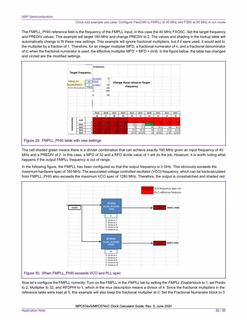
The FMPLL_PHI0 reference field is the frequency of the FMPLL input, in this case the 40 MHz FXOSC. Set the target frequencyand PREDIV values. This example will target 160 MHz and change PREDIV to 2. The values and shading in the lookup table willautomatically change to fit these new settings. This example will ignore fractional multipliers, but if it were used, it would add tothe multiplier by a fraction of 1. Therefore, for an integer multiplier MFD, a fractional numerator of n, and a fractional denominatorof d, when the fractional numerator is used, the effective multiplier MFD’ = MFD + (n/d). In the figure below, the table has changedand circled are the modified settings.
Figure 29. FMPLL_PHI0 table with new settings
The cell shaded green means there is a divider combination that can achieve exactly 160 MHz given an input frequency of 40MHz and a PREDIV of 2. In this case, a MFD of 32 and a RFD divide value of 1 will do the job. However, it is worth noting whathappens if the output FMPLL frequency is out of range.
In the following figure, the FMPLL has been configured so that the output frequency is 3 GHz. This obviously exceeds themaximum hardware spec of 160 MHz. The associated voltage controlled oscillator (VCO) frequency, which can be backcalculatedfrom FMPLL_PHI0 also exceeds the maximum VCO spec of 1280 MHz. Therefore, the output is crosshatched and shaded red.
Figure 30. When FMPLL_PHI0 exceeds VCO and PLL spec
Now let’s configure the FMPLL correctly. Turn on the FMPLL in the FMPLL tab by setting the FMPLL Enable block to 1, set Predivto 2, Multiplier to 32, and RFDPHI to 1, which in the mux description means a divisor of 4. Since the fractional multipliers in thereference table were kept at 0, this example will also keep the fractional multiplier at 0. Set the Fractional Numerator block to 0
NXP SemiconductorsClock tool example use case: Configure FlexCAN to FMPLL at 40 MHz and FS80 at 80 MHz in run mode
MPC574xG/MPC574xC Clock Calculator Guide, Rev. 5, June 2020Application Note 22 / 32
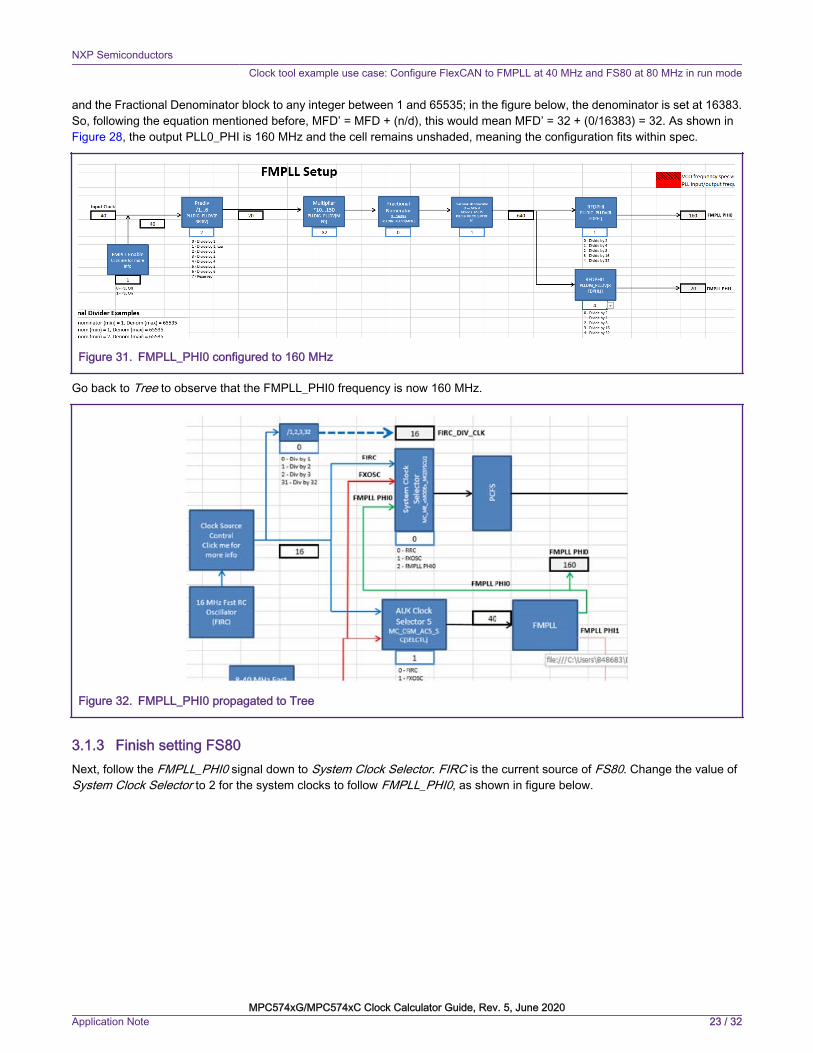
and the Fractional Denominator block to any integer between 1 and 65535; in the figure below, the denominator is set at 16383.So, following the equation mentioned before, MFD’ = MFD + (n/d), this would mean MFD’ = 32 + (0/16383) = 32. As shown in Figure 28, the output PLL0_PHI is 160 MHz and the cell remains unshaded, meaning the configuration fits within spec.
Figure 31. FMPLL_PHI0 configured to 160 MHz
Go back to Tree to observe that the FMPLL_PHI0 frequency is now 160 MHz.
Figure 32. FMPLL_PHI0 propagated to Tree
3.1.3 Finish setting FS80Next, follow the FMPLL_PHI0 signal down to System Clock Selector. FIRC is the current source of FS80. Change the value ofSystem Clock Selector to 2 for the system clocks to follow FMPLL_PHI0, as shown in figure below.
NXP SemiconductorsClock tool example use case: Configure FlexCAN to FMPLL at 40 MHz and FS80 at 80 MHz in run mode
MPC574xG/MPC574xC Clock Calculator Guide, Rev. 5, June 2020Application Note 23 / 32
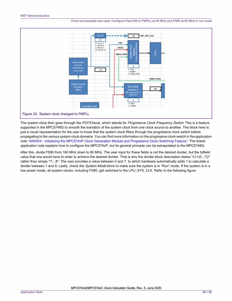
Figure 33. System clock changed to FMPLL
The system clock then goes through the PCFS block, which stands for Progressive Clock Frequency Switch. This is a featuresupported in the MPC5748G to smooth the transition of the system clock from one clock source to another. The block here isjust a visual representation for the user to know that the system clock filters through the progressive clock switch beforepropagating to the various system clock domains. You can find more information on the progressive clock switch in the applicationnote “AN5304 - Initializing the MPC574xP Clock Generation Module and Progressive Clock Switching Feature.” The linkedapplication note explains how to configure the MPC574xP, but its general principle can be extrapolated to the MPC5748G.
After this, divide FS80 from 160 MHz down to 80 MHz. The user input for these fields is not the desired divider, but the bitfieldvalue that one would have to enter to achieve the desired divider. That is why the divider block description states "/(1+(0...7))"rather than simply "/1...8". The user provides a value between 0 and 7, to which hardware automatically adds 1 to calculate adivider between 1 and 8. Lastly, check the System Mode block to make sure the system is in “Run” mode. If the system is in alow power mode, all system clocks, including FS80, get switched to the LPU_SYS_CLK. Refer to the following figure.
NXP SemiconductorsClock tool example use case: Configure FlexCAN to FMPLL at 40 MHz and FS80 at 80 MHz in run mode
MPC574xG/MPC574xC Clock Calculator Guide, Rev. 5, June 2020Application Note 24 / 32

Figure 34. FS80 at 80 MHz FMPLL
For example, if the FS80 divider bitfield value is 0, the actual divider would be 1, which would make FS80 160 MHz. This wouldexceed the maximum allowable FS80 frequency of 80 MHz. The tool highlights the FS80 cell red to signify that such a frequencyis not allowed, as shown in the following figure.
NXP SemiconductorsClock tool example use case: Configure FlexCAN to FMPLL at 40 MHz and FS80 at 80 MHz in run mode
MPC574xG/MPC574xC Clock Calculator Guide, Rev. 5, June 2020Application Note 25 / 32
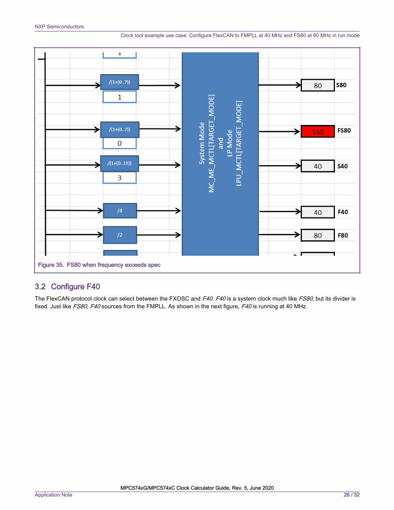
Figure 35. FS80 when frequency exceeds spec
3.2 Configure F40The FlexCAN protocol clock can select between the FXOSC and F40. F40 is a system clock much like FS80, but its divider isfixed. Just like FS80, F40 sources from the FMPLL. As shown in the next figure, F40 is running at 40 MHz.
NXP SemiconductorsClock tool example use case: Configure FlexCAN to FMPLL at 40 MHz and FS80 at 80 MHz in run mode
MPC574xG/MPC574xC Clock Calculator Guide, Rev. 5, June 2020Application Note 26 / 32
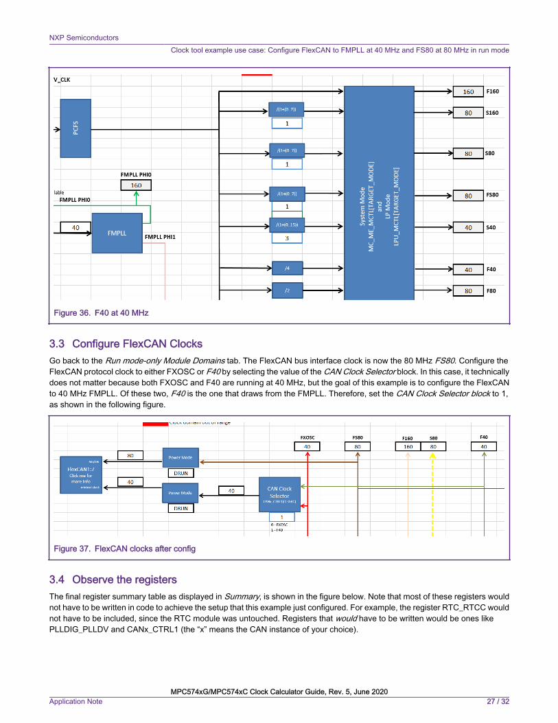
Figure 36. F40 at 40 MHz
3.3 Configure FlexCAN ClocksGo back to the Run mode-only Module Domains tab. The FlexCAN bus interface clock is now the 80 MHz FS80. Configure theFlexCAN protocol clock to either FXOSC or F40 by selecting the value of the CAN Clock Selector block. In this case, it technicallydoes not matter because both FXOSC and F40 are running at 40 MHz, but the goal of this example is to configure the FlexCANto 40 MHz FMPLL. Of these two, F40 is the one that draws from the FMPLL. Therefore, set the CAN Clock Selector block to 1,as shown in the following figure.
Figure 37. FlexCAN clocks after config
3.4 Observe the registersThe final register summary table as displayed in Summary, is shown in the figure below. Note that most of these registers wouldnot have to be written in code to achieve the setup that this example just configured. For example, the register RTC_RTCC wouldnot have to be included, since the RTC module was untouched. Registers that would have to be written would be ones likePLLDIG_PLLDV and CANx_CTRL1 (the “x” means the CAN instance of your choice).
NXP SemiconductorsClock tool example use case: Configure FlexCAN to FMPLL at 40 MHz and FS80 at 80 MHz in run mode
MPC574xG/MPC574xC Clock Calculator Guide, Rev. 5, June 2020Application Note 27 / 32
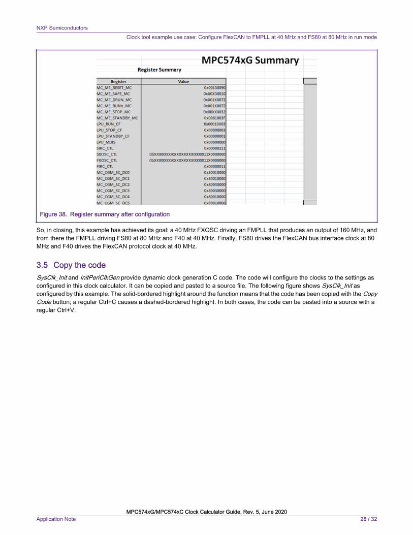
Figure 38. Register summary after configuration
So, in closing, this example has achieved its goal: a 40 MHz FXOSC driving an FMPLL that produces an output of 160 MHz, andfrom there the FMPLL driving FS80 at 80 MHz and F40 at 40 MHz. Finally, FS80 drives the FlexCAN bus interface clock at 80MHz and F40 drives the FlexCAN protocol clock at 40 MHz.
3.5 Copy the codeSysClk_Init and InitPeriClkGen provide dynamic clock generation C code. The code will configure the clocks to the settings asconfigured in this clock calculator. It can be copied and pasted to a source file. The following figure shows SysClk_Init asconfigured by this example. The solid-bordered highlight around the function means that the code has been copied with the CopyCode button; a regular Ctrl+C causes a dashed-bordered highlight. In both cases, the code can be pasted into a source with aregular Ctrl+V.
NXP SemiconductorsClock tool example use case: Configure FlexCAN to FMPLL at 40 MHz and FS80 at 80 MHz in run mode
MPC574xG/MPC574xC Clock Calculator Guide, Rev. 5, June 2020Application Note 28 / 32
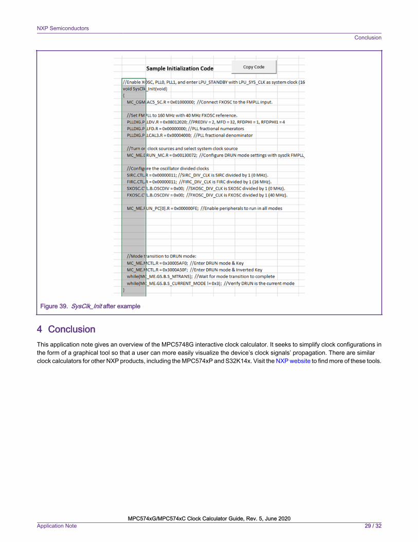
Figure 39. SysClk_Init after example
4 ConclusionThis application note gives an overview of the MPC5748G interactive clock calculator. It seeks to simplify clock configurations inthe form of a graphical tool so that a user can more easily visualize the device’s clock signals’ propagation. There are similarclock calculators for other NXP products, including the MPC574xP and S32K14x. Visit the NXP website to find more of these tools.
NXP SemiconductorsConclusion
MPC574xG/MPC574xC Clock Calculator Guide, Rev. 5, June 2020Application Note 29 / 32

5 Revision history
Rev. No. Date Substantive Change(s)
0 January 2017 Initial version
1 January 2017 Updates to the SAI Clocking section
2 April 2017 1. The following new sections have been added:
• CAN Clocking
• Summary
• Observe the register
2. The following images have been replaced:
• Clock calculator tree
• F40 at 40 MHz
• FS80 at 80 MHz FMPLL
• FS80 to oscillators
• FS80, Tree tab
• FS80 when frequency exceeds spec
3. Editorial updates through out the document
3 June 2017 1. The following new section has been added:
• Copy the code
2. The following images have been replaced:
• Clock calculator tree
• Clock source control
• One of the module domains
• ENET clocking
• FMPLL control
• FlexCAN clocks
• FS80 to oscillators
• FXOSC control
Tablecontinues
on the nextpage...
NXP SemiconductorsRevision history
MPC574xG/MPC574xC Clock Calculator Guide, Rev. 5, June 2020Application Note 30 / 32

Tablecontinuedfrom thepreviouspage...
Rev. No. Date Substantive Change(s)
• FMPLL calculator
• FMPLL PHI0 configured to 160 MHz
• FS80 at 80 MHz FMPLL
• FS80 when frequency exceeds spec
• F40 at 40 MHz
• FlexCAN clocks after config
3. The following sections have been updated:
• Introduction
• Configure FMPLL
• Tree
• Summary
4 Ocober 2017 Updated the associated MPC574xC_Clock_Calculator andMPC574xG_Clock_Calculator files
5 June 2020 Updated the associated MPC574xC_Clock_Calculator andMPC574xG_Clock_Calculator files
NXP SemiconductorsRevision history
MPC574xG/MPC574xC Clock Calculator Guide, Rev. 5, June 2020Application Note 31 / 32

How To Reach Us
Home Page:
nxp.com
Web Support:
nxp.com/support
Information in this document is provided solely to enable system and software implementers touse NXP products. There are no express or implied copyright licenses granted hereunder todesign or fabricate any integrated circuits based on the information in this document. NXPreserves the right to make changes without further notice to any products herein.
NXP makes no warranty, representation, or guarantee regarding the suitability of its products forany particular purpose, nor does NXP assume any liability arising out of the application or useof any product or circuit, and specifically disclaims any and all liability, including without limitationconsequential or incidental damages. “Typical” parameters that may be provided in NXP datasheets and/or specifications can and do vary in different applications, and actual performancemay vary over time. All operating parameters, including “typicals,” must be validated for eachcustomer application by customer's technical experts. NXP does not convey any license underits patent rights nor the rights of others. NXP sells products pursuant to standard terms andconditions of sale, which can be found at the following address: nxp.com/SalesTermsandConditions.
While NXP has implemented advanced security features, all products may be subject tounidentified vulnerabilities. Customers are responsible for the design and operation of theirapplications and products to reduce the effect of these vulnerabilities on customer’s applicationsand products, and NXP accepts no liability for any vulnerability that is discovered. Customersshould implement appropriate design and operating safeguards to minimize the risks associatedwith their applications and products.
NXP, the NXP logo, NXP SECURE CONNECTIONS FOR A SMARTER WORLD, COOLFLUX,EMBRACE, GREENCHIP, HITAG, I2C BUS, ICODE, JCOP, LIFE VIBES, MIFARE, MIFARECLASSIC, MIFARE DESFire, MIFARE PLUS, MIFARE FLEX, MANTIS, MIFARE ULTRALIGHT,MIFARE4MOBILE, MIGLO, NTAG, ROADLINK, SMARTLX, SMARTMX, STARPLUG, TOPFET,TRENCHMOS, UCODE, Freescale, the Freescale logo, AltiVec, C‑5, CodeTEST, CodeWarrior,ColdFire, ColdFire+, C‑Ware, the Energy Efficient Solutions logo, Kinetis, Layerscape, MagniV,mobileGT, PEG, PowerQUICC, Processor Expert, QorIQ, QorIQ Qonverge, Ready Play,SafeAssure, the SafeAssure logo, StarCore, Symphony, VortiQa, Vybrid, Airfast, BeeKit,BeeStack, CoreNet, Flexis, MXC, Platform in a Package, QUICC Engine, SMARTMOS, Tower,TurboLink, and UMEMS are trademarks of NXP B.V. All other product or service names are theproperty of their respective owners. AMBA, Arm, Arm7, Arm7TDMI, Arm9, Arm11, Artisan,big.LITTLE, Cordio, CoreLink, CoreSight, Cortex, DesignStart, DynamIQ, Jazelle, Keil, Mali,Mbed, Mbed Enabled, NEON, POP, RealView, SecurCore, Socrates, Thumb, TrustZone, ULINK,ULINK2, ULINK-ME, ULINK-PLUS, ULINKpro, µVision, Versatile are trademarks or registeredtrademarks of Arm Limited (or its subsidiaries) in the US and/or elsewhere. The relatedtechnology may be protected by any or all of patents, copyrights, designs and trade secrets. Allrights reserved. Oracle and Java are registered trademarks of Oracle and/or its affiliates. ThePower Architecture and Power.org word marks and the Power and Power.org logos and relatedmarks are trademarks and service marks licensed by Power.org.
© NXP B.V. 2020. All rights reserved.
For more information, please visit: http://www.nxp.comFor sales office addresses, please send an email to: [email protected]
Date of release: June 2020Document identifier: AN5392