Embed Size (px)
Citation preview
AN869External Memory Interfacing Techniques for the PIC18F8XXX
INTRODUCTION
The PIC18FXXXX family offers the largest range ofon-chip enhanced FLASH program memory and therichest selection of peripherals in the current line ofMicrochip microcontrollers. The PIC18F8XXX subset ismade up of 80-pin parts that further extend the capabil-ities by providing access to external memory devices.Through the addition of external memory devices, an8-bit application has the power to utilize unprecedentedamounts of code or data; up to 2 Mbytes for an 8-bitmicrocontroller!
This application note describes the methodology toutilize the External Memory Interface on thePIC18F8XXX family of parts, and elaborates on theinformation provided in the data sheet. Connectiondiagrams are provided to demonstrate implementingvarious memory configurations. C and assembly codeexamples are included to assist in softwaredevelopment. It is expected that the reader be familiarwith the PIC18 architecture and instruction set.
This application note contains the following mainsections:
• External Memory Interface (EMI) Overview
Describes the Operating modes, pin implementation,registers, and control bits that determine thefunctionality of the External Memory Interface.
• EMI Functional Implementation
Discusses the mechanics behind the PIC18F8XXX16-bit EMI. The most common operations of programfetching, user controlled reads, and user controlledwrites are described.
• 16-bit EMI Operating Modes
Details the timing and connection of the three EMImodes available to the PIC18F8XXX.
• 8-bit EMI Solutions
Explains hardware and software concepts that allowaccess to byte-sized memories.
• The Chip Enable Line and EMI Memory Mapped Peripherals
Proposes a simple solution to using memory mappedperipherals in a PIC18F8XXX system.
FIGURE 1: EXTERNAL MEMORY INTERFACE DIAGRAM
Author: Tim RovnakMicrochip Technology Inc.
PIC
18F
8XX
X
Interface MemoryLogic
EMI BusData
Address,Control
2003 Microchip Technology Inc. DS00869B-page 1
AN869
EXTERNAL MEMORY INTERFACE (EMI) OVERVIEW
External Memory Interface offers the user manyoptions, including:
• Operating the microcontroller entirely from external memory
• Using combinations of on-chip and external memory up to the 2-Mbyte limit
• Using external FLASH or EEPROM memory for reprogrammable application code or large data tables
• Using external RAM devices for storing large amounts of program or variable data
• Using external memory mapped devices and peripherals
EMI Operating Modes
There are four distinct EMI Operating modes availableto the PIC18F8XXX devices. The EMI mode is deter-mined by setting the two Least Significant bits of theCONFIG3L configuration byte. The function of theWAIT bit is described later in this application note. Formore information on programming CONFIG bits,please see the “Special Features of the CPU” sectionin the respective data sheet.
Following is a summary for each of the ExternalMemory Interface modes:
MC – The Microcontroller Mode accesses only on-chipFLASH memory. External Memory Interface functionsare disabled. Attempts to read above the physical limit ofthe on-chip FLASH causes a read of all ‘0’s (a NOPinstruction).
MP – The Microprocessor Mode permits executionand access only through external program memory; thecontents of the on-chip FLASH memory are ignored.The 21-bit program counter permits access to a 2-Mbytelinear program memory space.
MPBB – The Microprocessor with Boot Block Modeaccesses on-chip FLASH memory within only the bootblock. The boot block size is device dependent and islocated at the beginning of program memory. Beyondthe boot block, external program memory is accessedall the way up to the 2-MByte limit. Program executionautomatically switches between the two memories asrequired.
EMC – The Extended Microcontroller Mode allowsaccess to both internal and external program memoriesas a single block. The device can access its entire on-chip FLASH memory; above this, the device accessesexternal program memory up to the 2-MByte programspace limit. As with Boot Block mode, execution auto-matically switches between the two memories asrequired.
REGISTER 1: CONFIG3L CONFIGURATION BYTE R/P-1 U-0 U-0 U-0 U-0 U-0 R/P-1 R/P-1
WAIT — — — — — PM1 PM0
bit 7 bit 0
bit 7 WAIT: External Bus Data Wait Enable bit1 = Wait selections unavailable, device will not wait 0 = Wait programmed by WAIT1 and WAIT0 bits of MEMCOM register (MEMCOM<5:4>)
bit 6-2 Unimplemented: Read as ‘0’
bit 1-0 PM1:PM0: Processor Data Memory Mode Select bits11 = Microcontroller mode10 = Microprocessor mode01 = Microcontroller with Boot Block mode 00 = Extended Microcontroller mode
Legend:
R = Readable bit P = Programmable bit U = Unimplemented bit, read as ‘0’
- n = Value after erase ‘1’ = Bit is set ‘0’ = Bit is cleared x = Bit is unknown
DS00869B-page 2 2003 Microchip Technology Inc.
AN869
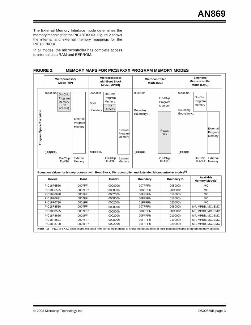
The External Memory Interface mode determines thememory mapping for the PIC18F8XXX. Figure 2 showsthe internal and external memory mappings for thePIC18F8XXX.
In all modes, the microcontroller has complete accessto internal data RAM and EEPROM.
FIGURE 2: MEMORY MAPS FOR PIC18FXXX PROGRAM MEMORY MODES
MicroprocessorMode (MP)
000000h
1FFFFFh
ExternalProgramMemory
ExternalProgramMemory
1FFFFFh
000000h
On-ChipProgramMemory
ExtendedMicrocontroller
Mode (EMC)
MicrocontrollerMode (MC)
000000h
ExternalOn-Chip
Pro
gra
m S
pace
Exe
cuti
on
On-ChipProgramMemory
1FFFFFh
Reads
Boundary
1FFFFFh
Boot
Microprocessorwith Boot BlockMode (MPBB)
000000h
ExternalProgramMemory
MemoryFLASH
On-ChipProgramMemory
(Noaccess)
‘0’s
ExternalOn-ChipMemoryFLASH
On-ChipFLASH
ExternalMemory
Boundary Values for Microprocessor with Boot Block, Microcontroller and Extended Microcontroller modes(1)
Note 1: PIC18F6X2X devices are included here for completeness to show the boundaries of their boot blocks and program memory spaces.
Device Boot Boot+1 Boundary Boundary+1 Available Memory Mode(s)
PIC18F6520 0007FFh 000800h 007FFFh 008000h MC
PIC18F6525 0007FFh 000800h 00BFFFh 00C000h MC
PIC18F6620 0001FFh 000200h 00FFFFh 010000h MCPIC18F6621 0007FFh 000800h 00FFFFh 010000h MCPIC18F6720 0001FFh 000200h 01FFFFh 020000h MC
PIC18F8520 0007FFh 000800h 007FFFh 008000h MP, MPBB, MC, EMC
PIC18F8525 0007FFh 000800h 00BFFFh 00C000h MP, MPBB, MC, EMC
PIC18F8620 0001FFh 000200h 00FFFFh 010000h MP, MPBB, MC, EMC
PIC18F8621 0007FFh 000800h 00FFFFh 010000h MP, MPBB, MC, EMCPIC18F8720 0001FFh 000200h 01FFFFh 020000h MP, MPBB, MC, EMC
BoundaryBoundary+1
BoundaryBoundary+1
On-ChipProgramMemory
On-ChipFLASH
NoAccess
2003 Microchip Technology Inc. DS00869B-page 3
AN869
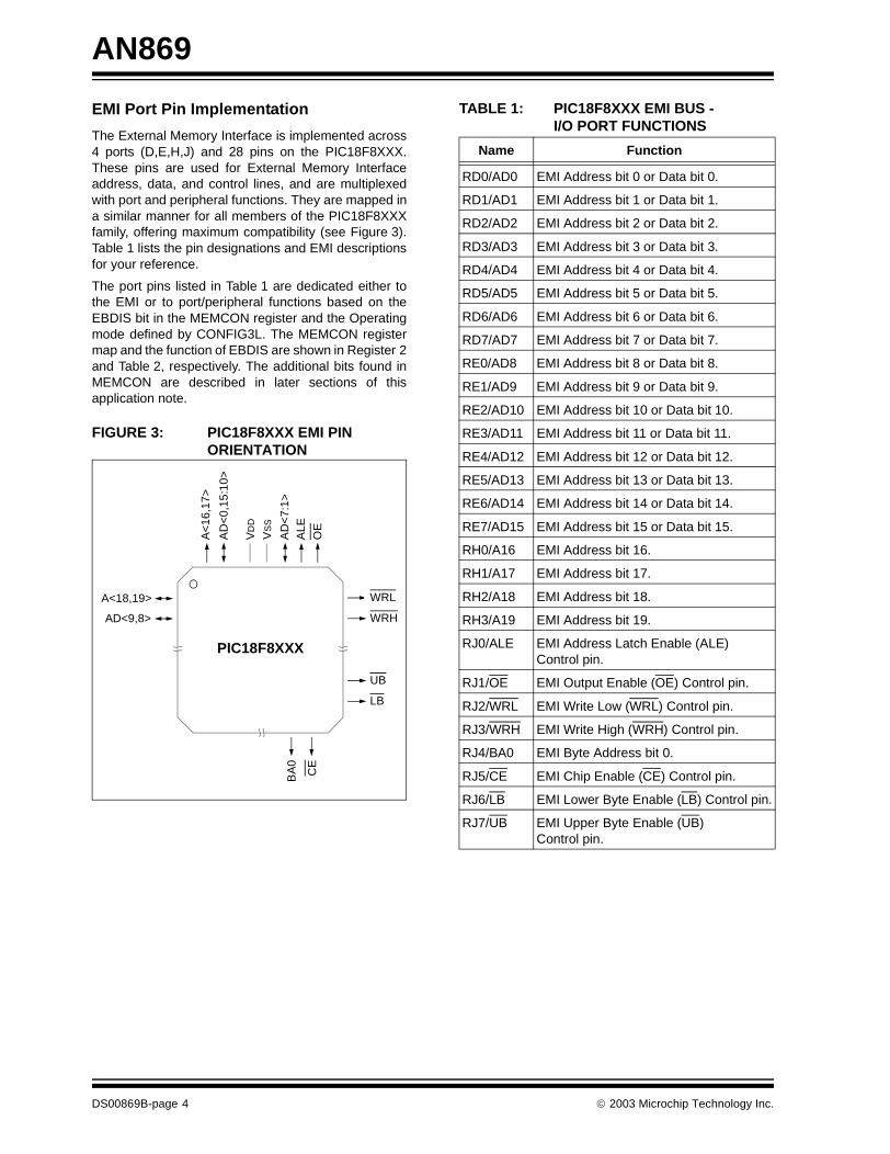
EMI Port Pin Implementation
The External Memory Interface is implemented across4 ports (D,E,H,J) and 28 pins on the PIC18F8XXX.These pins are used for External Memory Interfaceaddress, data, and control lines, and are multiplexedwith port and peripheral functions. They are mapped ina similar manner for all members of the PIC18F8XXXfamily, offering maximum compatibility (see Figure 3).Table 1 lists the pin designations and EMI descriptionsfor your reference.
The port pins listed in Table 1 are dedicated either tothe EMI or to port/peripheral functions based on theEBDIS bit in the MEMCON register and the Operatingmode defined by CONFIG3L. The MEMCON registermap and the function of EBDIS are shown in Register 2and Table 2, respectively. The additional bits found inMEMCON are described in later sections of thisapplication note.
FIGURE 3: PIC18F8XXX EMI PIN ORIENTATION
TABLE 1: PIC18F8XXX EMI BUS - I/O PORT FUNCTIONS
PIC18F8XXX
A<18,19> WRL
WRH
UB
LB
CE
BA
0
AD<9,8>
A<
16,1
7>
AD
<0,
15:1
0>
AD
<7:
1>A
LEO
E
VS
S
VD
D
Name Function
RD0/AD0 EMI Address bit 0 or Data bit 0.
RD1/AD1 EMI Address bit 1 or Data bit 1.
RD2/AD2 EMI Address bit 2 or Data bit 2.
RD3/AD3 EMI Address bit 3 or Data bit 3.
RD4/AD4 EMI Address bit 4 or Data bit 4.
RD5/AD5 EMI Address bit 5 or Data bit 5.
RD6/AD6 EMI Address bit 6 or Data bit 6.
RD7/AD7 EMI Address bit 7 or Data bit 7.
RE0/AD8 EMI Address bit 8 or Data bit 8.
RE1/AD9 EMI Address bit 9 or Data bit 9.
RE2/AD10 EMI Address bit 10 or Data bit 10.
RE3/AD11 EMI Address bit 11 or Data bit 11.
RE4/AD12 EMI Address bit 12 or Data bit 12.
RE5/AD13 EMI Address bit 13 or Data bit 13.
RE6/AD14 EMI Address bit 14 or Data bit 14.
RE7/AD15 EMI Address bit 15 or Data bit 15.
RH0/A16 EMI Address bit 16.
RH1/A17 EMI Address bit 17.
RH2/A18 EMI Address bit 18.
RH3/A19 EMI Address bit 19.
RJ0/ALE EMI Address Latch Enable (ALE) Control pin.
RJ1/OE EMI Output Enable (OE) Control pin.
RJ2/WRL EMI Write Low (WRL) Control pin.
RJ3/WRH EMI Write High (WRH) Control pin.
RJ4/BA0 EMI Byte Address bit 0.
RJ5/CE EMI Chip Enable (CE) Control pin.
RJ6/LB EMI Lower Byte Enable (LB) Control pin.
RJ7/UB EMI Upper Byte Enable (UB) Control pin.
DS00869B-page 4 2003 Microchip Technology Inc.
AN869
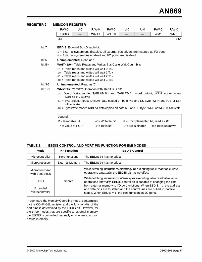
REGISTER 2: MEMCON REGISTER
In summary, the Memory Operating mode is determinedby the CONFIG3L register and the functionality of theport pins is determined by the EBDIS bit. However, forthe three modes that are specific to external memory,the EBDIS is controlled manually only when executionoccurs internally.
R/W-0 U-0 R/W-0 R/W-0 U-0 U-0 R/W-0 R/W-0
EBDIS — WAIT1 WAIT0 — — WM1 WM0
bit7 bit0
bit 7 EBDIS: External Bus Disable bit1 = External system bus disabled, all external bus drivers are mapped as I/O ports0 = External system bus enabled and I/O ports are disabled
bit 6 Unimplemented: Read as ‘0’
bit 5-4 WAIT<1:0>: Table Reads and Writes Bus Cycle Wait Count bits
11 = Table reads and writes will wait 0 TCY
10 = Table reads and writes will wait 1 TCY
01 = Table reads and writes will wait 2 TCY
00 = Table reads and writes will wait 3 TCY
bit 3-2 Unimplemented: Read as ‘0’
bit 1-0 WM<1:0>: TBLWRT Operation with 16-bit Bus bits1x = Word Write mode: TABLAT<0> and TABLAT<1> word output, WRH active when
TABLAT<1> written01 = Byte Select mode: TABLAT data copied on both MS and LS Byte, WRH and (UB or LB)
will activate00 = Byte Write mode: TABLAT data copied on both MS and LS Byte, WRH or WRL will activate
Legend:
R = Readable bit W = Writable bit U = Unimplemented bit, read as ‘0’
- n = Value at POR ‘1’ = Bit is set ‘0’ = Bit is cleared x = Bit is unknown
TABLE 2: EBDIS CONTROL AND PORT PIN FUNCTION FOR EMI MODES
Mode Pin Function EBDIS Control
Microcontroller Port Functions The EBDIS bit has no effect.
Microprocessor External Memory The EBDIS bit has no effect.
Microprocessor with Boot Block
AND
Extended Microcontroller
Shared
While fetching instructions externally or executing table read/table write operations externally, the EBDIS bit has no effect.
While fetching instructions internally or executing table read/table write operations internally, EBDIS control bit is capable of changing the pins from external memory to I/O port functions. When EBDIS = 0, the address and data pins are tri-stated and the control lines are pulled to inactive states. When EBDIS = 1, the pins function as I/O ports.
2003 Microchip Technology Inc. DS00869B-page 5
AN869
EMI FUNCTIONAL IMPLEMENTATION
The three most common functions of the ExternalMemory Interface are:
• Program Fetches
• Data Reads• Data Writes
This section describes how these operations areexecuted by the EMI. As will be shown, the timings forprogram fetches and data reads are almost identical.Data writes are presented generically here andspecifics are detailed in a later section.
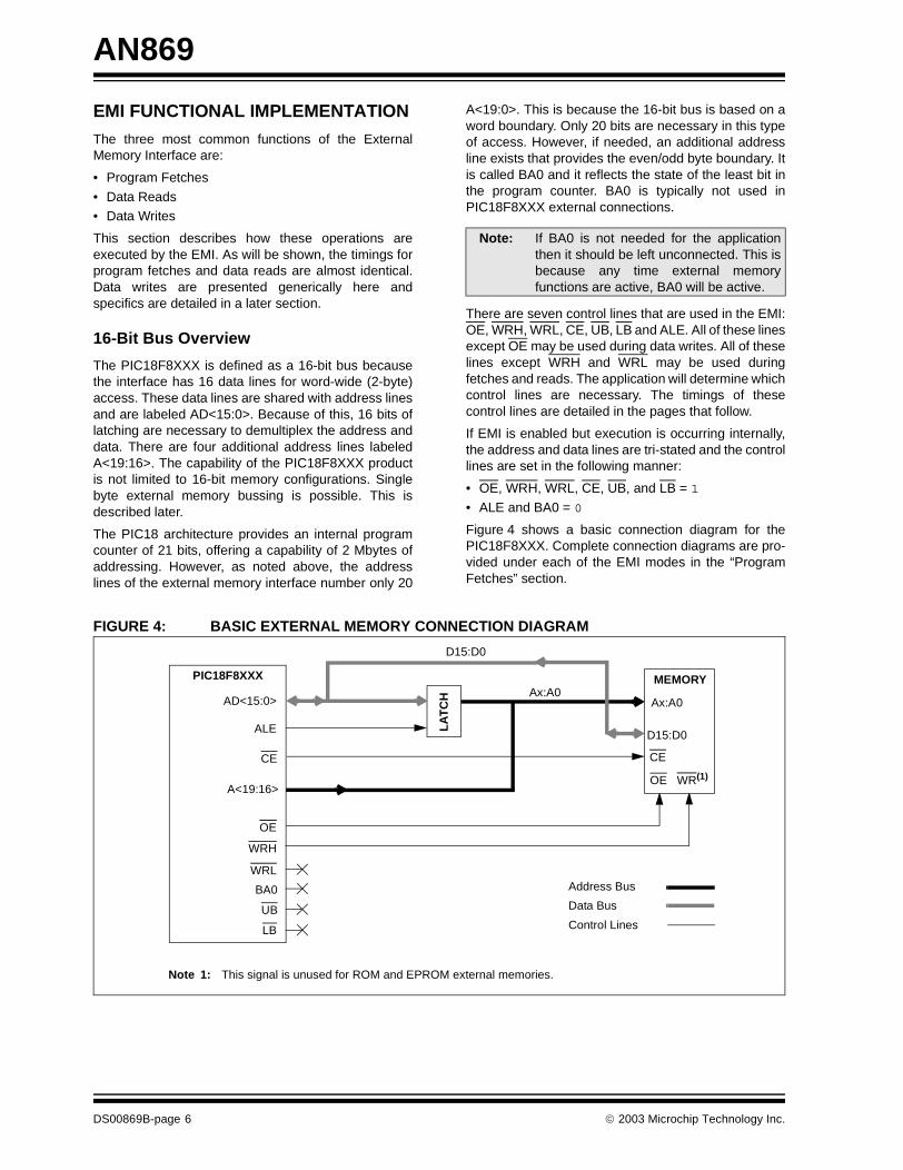
16-Bit Bus Overview
The PIC18F8XXX is defined as a 16-bit bus becausethe interface has 16 data lines for word-wide (2-byte)access. These data lines are shared with address linesand are labeled AD<15:0>. Because of this, 16 bits oflatching are necessary to demultiplex the address anddata. There are four additional address lines labeledA<19:16>. The capability of the PIC18F8XXX productis not limited to 16-bit memory configurations. Singlebyte external memory bussing is possible. This isdescribed later.
The PIC18 architecture provides an internal programcounter of 21 bits, offering a capability of 2 Mbytes ofaddressing. However, as noted above, the addresslines of the external memory interface number only 20
A<19:0>. This is because the 16-bit bus is based on aword boundary. Only 20 bits are necessary in this typeof access. However, if needed, an additional addressline exists that provides the even/odd byte boundary. Itis called BA0 and it reflects the state of the least bit inthe program counter. BA0 is typically not used inPIC18F8XXX external connections.
There are seven control lines that are used in the EMI:OE, WRH, WRL, CE, UB, LB and ALE. All of these linesexcept OE may be used during data writes. All of theselines except WRH and WRL may be used duringfetches and reads. The application will determine whichcontrol lines are necessary. The timings of thesecontrol lines are detailed in the pages that follow.
If EMI is enabled but execution is occurring internally,the address and data lines are tri-stated and the controllines are set in the following manner:
• OE, WRH, WRL, CE, UB, and LB = 1
• ALE and BA0 = 0
Figure 4 shows a basic connection diagram for thePIC18F8XXX. Complete connection diagrams are pro-vided under each of the EMI modes in the “ProgramFetches” section.
FIGURE 4: BASIC EXTERNAL MEMORY CONNECTION DIAGRAM
Note: If BA0 is not needed for the applicationthen it should be left unconnected. This isbecause any time external memoryfunctions are active, BA0 will be active.
AD<15:0>
PIC18F8XXX
OE
WRH
LA
TC
H Ax:A0
D15:D0
OE WR(1)
CE
ALE
D15:D0
Ax:A0
Note 1: This signal is unused for ROM and EPROM external memories.
A<19:16>
CE
Address Bus
Data Bus
Control Lines
WRL
BA0
UB
LB
MEMORY
DS00869B-page 6 2003 Microchip Technology Inc.
AN869
Program Fetches
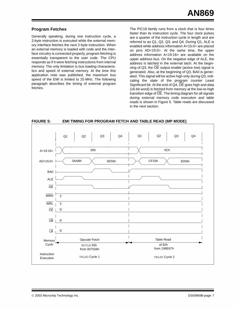
Generally speaking, during one instruction cycle, a2-byte instruction is executed while the external mem-ory interface fetches the next 2-byte instruction. Whenan external memory is loaded with code and the inter-face circuitry is connected properly, program fetching isessentially transparent to the user code. The CPUresponds as if it were fetching instructions from internalmemory. The only limitation is bus loading characteris-tics and speed of external memory. At the time thisapplication note was published, the maximum busspeed of the EMI is limited to 25 MHz. The followingparagraph describes the timing of external programfetches.
The PIC18 family runs from a clock that is four timesfaster than its instruction cycle. The four clock pulsesare a quarter of the instruction cycle in length and arereferred to as Q1, Q2, Q3, and Q4. During Q1, ALE isenabled while address information A<15:0> are placedon pins AD<15:0>. At the same time, the upperaddress information A<19:16> are available on theupper address bus. On the negative edge of ALE, theaddress is latched in the external latch. At the begin-ning of Q3, the OE output enable (active low) signal isgenerated. Also, at the beginning of Q3, BA0 is gener-ated. This signal will be active high only during Q3, indi-cating the state of the program counter LeastSignificant bit. At the end of Q4, OE goes high and data(16-bit word) is fetched from memory at the low-to-hightransition edge of OE. The timing diagram for all signalsduring external memory code execution and tablereads is shown in Figure 5. Table reads are discussedin the next section.
FIGURE 5: EMI TIMING FOR PROGRAM FETCH AND TABLE READ (MP MODE)
ALE
OE
WRH
WRL
AD<15:0>
BA0
A<19:16>
CE
MemoryCycle
InstructionExecution
UB
LB
00h 0Ch
0E55h CF33h 9256h
‘1’
‘1’
‘0’
‘0’
‘0’
Q3 Q4 Q1 Q2 Q3 Q4
TBLRD Cycle 1 TBLRD Cycle 2
Opcode Fetch Table Read
MOVLW 55hfrom 007556h
of 92hfrom 199E67h
3AABh
Q1 Q2
2003 Microchip Technology Inc. DS00869B-page 7
AN869
Table Reads
The user code controls data reads through the use oftable reads which are very similar to program fetching.The timings are essentially the same (see the previoussection) but unlike program fetching, reads areexecuted on a single byte basis. Therefore, the controlsignal BA0 is the only signal that behaves differently(see Figure 5). The mechanics of table reads can befound in the following sections.
TABLE REGISTERS
The following two control registers are used inconjunction with the table read instructions:
• TABLAT register• TBLPTR registers
The table latch (TABLAT) is an 8-bit Special FunctionRegister (SFR). The table latch is used to hold 8-bitdata obtained from the read of program memory(internal or external).
The table pointer (TBLPTR) addresses a byte ofprogram memory (internal or external). The TBLPTR ismade up of three Special Function Registers:
• Table Pointer Upper byte (TBLPTRU)
• Table Pointer High byte (TBLPTRH)• Table Pointer Low byte (TBLPTRL)
These three registers join to form a 21-bit wide pointerwhich allows the device to address up to 2 Mbytes ofprogram memory space. These registers are similarlyused in data write operations.
TABLE READ INSTRUCTION (TBLRD*)
The TBLRD* instruction is used to retrieve data frominternal or external program memory and places it intodata memory. TBLPTR points to a byte address in pro-gram memory space. Executing TBLRD* places thebyte into TABLAT. In addition, TBLPTR can be modifiedautomatically for the next table read operation:
• TBLRD*+ (post-increment)
• TBLRD*- (post-decrement)• TBLRD+* (pre-increment)
During table read operations, the Least Significant bitof TBLPTR is copied to BA0. The values ofTBLPTR<20:1> appear on address pins A<19:0>.Next, 16-bits of data are read on to the data bus. Cir-cuitry in TABLAT will select either the high or the lowbyte of the data from the 16-bit bus, based on the LeastSignificant bit of the address. That is, when LSb is ‘0’,the lower byte (D<7:0>) is selected; when LSb is ‘1’, theupper byte (D<15:8>) is selected.
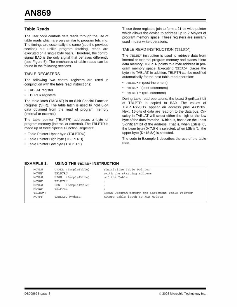
The code in Example 1 describes the use of the tableread.
EXAMPLE 1: USING THE TBLRD* INSTRUCTIONMOVLW UPPER (SampleTable) ;Initialize Table PointerMOVWF TBLPTRU ;with the starting addressMOVLW HIGH (SampleTable) ;of the TableMOVWF TBLPTRH ;MOVLW LOW (SampleTable) ;MOVWF TBLPTRL ;TBLRD*+ ;Read Program memory and increment Table PointerMOVFF TABLAT, Mydata ;Store table latch to FSR Mydata
DS00869B-page 8 2003 Microchip Technology Inc.
AN869
Table Writes
The user code controls data writes through the use oftable writes. Table write timing is dependent on the EMImode (detailed in the “16-Bit EMI Operating Modes”section).
TABLE REGISTERS
In a manner similar to reads, TABLAT and TBLPTR arealso used during writes. TABLAT holds the data bytethat will be used in the write operation. The address ofthe program memory (internal or external) location isspecified by TBLPTR.
TABLE WRITE INSTRUCTION (TBLWT*)
The TBLWT* instruction is used in the process thatwrites to program memory. TBLPTR can be modifiedautomatically for the next table write operation:
• TBLWT*+ (post-increment)
• TBLWT*- (post-decrement)• TBLWT+* (pre-increment)
When a TBLWT* is executed, the Least Significant bitof TBLPTR is copied to BA0 and the values ofTBLPTR<20:1> appear on address pins A<19:0>.Then, depending on the EMI mode and the TBLPTRaddress, data may be presented on the data bus. Thisis explained below.
When a TBLWT* is executed that causes data to bephysically placed on the bus, the data is always in theform of two bytes. These 16 bits may contain two indi-vidual bytes or may contain 1 byte copied. Thisdepends on the EMI. Then, based on the state of thecontrol lines, either one or both bytes will be written tothe external memory device during a single instructioncycle.
Word Write mode (detailed in “16-Bit EMI OperatingModes”) is a special case where a one-byte holdingregister is used in conjunction with TABLAT. DuringTBLWT* instructions to even addresses, the holdingregister is loaded but no data is presented externally.During TBLWT* instructions to odd addresses, the hold-ing register and the TABLAT are presented on the databus and written at the same time during one instructioncycle.
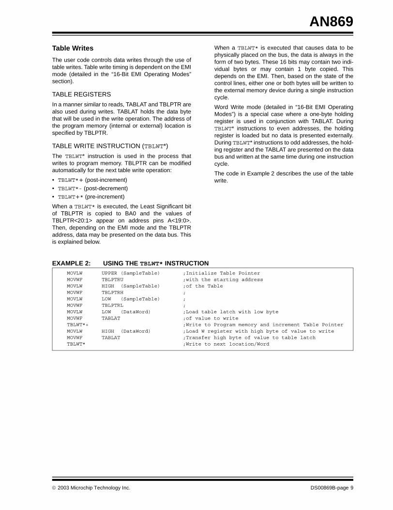
The code in Example 2 describes the use of the tablewrite.
EXAMPLE 2: USING THE TBLWT* INSTRUCTIONMOVLW UPPER (SampleTable) ;Initialize Table PointerMOVWF TBLPTRU ;with the starting addressMOVLW HIGH (SampleTable) ;of the TableMOVWF TBLPTRH ;MOVLW LOW (SampleTable) ;MOVWF TBLPTRL ;MOVLW LOW (DataWord) ;Load table latch with low byteMOVWF TABLAT ;of value to writeTBLWT*+ ;Write to Program memory and increment Table PointerMOVLW HIGH (DataWord) ;Load W register with high byte of value to writeMOVWF TABLAT ;Transfer high byte of value to table latchTBLWT* ;Write to next location/Word
2003 Microchip Technology Inc. DS00869B-page 9
AN869
16-BIT EMI OPERATING MODES
This section details the operation of the EMI Operatingmodes that are determined by the two LSbs of theMEMCON register. The EMI Operating mode chosendictates the appropriate types of external memoryavailable, and the method for connection.
MEMCON<1:0>
• 1x = Word Write Mode
• 01 = Byte Select Mode• 00 = Byte Write Mode
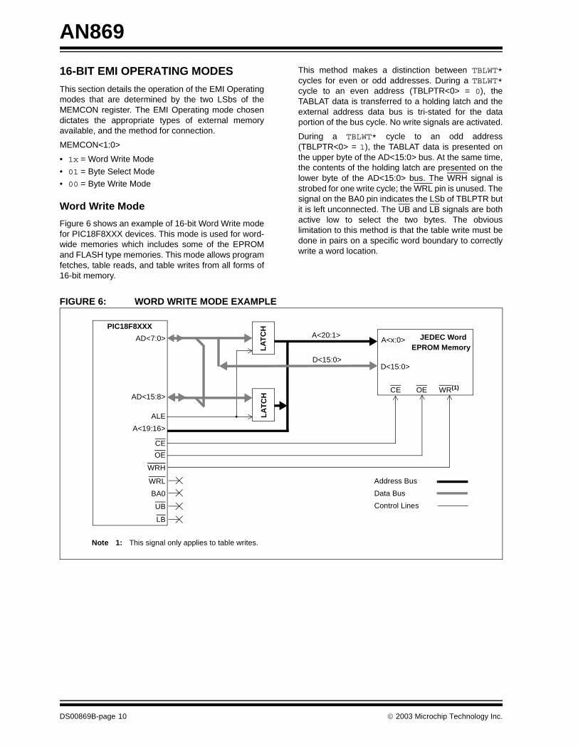
Word Write Mode
Figure 6 shows an example of 16-bit Word Write modefor PIC18F8XXX devices. This mode is used for word-wide memories which includes some of the EPROMand FLASH type memories. This mode allows programfetches, table reads, and table writes from all forms of16-bit memory.
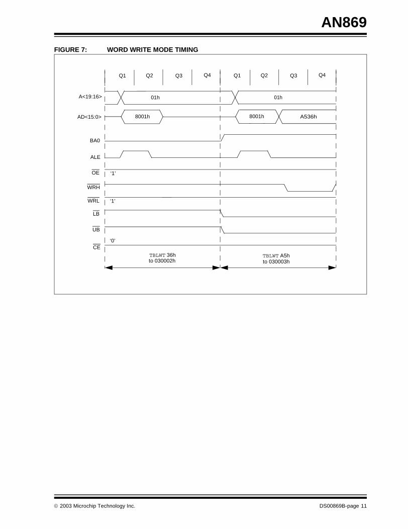
This method makes a distinction between TBLWT*cycles for even or odd addresses. During a TBLWT*cycle to an even address (TBLPTR<0> = 0), theTABLAT data is transferred to a holding latch and theexternal address data bus is tri-stated for the dataportion of the bus cycle. No write signals are activated.
During a TBLWT* cycle to an odd address(TBLPTR<0> = 1), the TABLAT data is presented onthe upper byte of the AD<15:0> bus. At the same time,the contents of the holding latch are presented on thelower byte of the AD<15:0> bus. The WRH signal isstrobed for one write cycle; the WRL pin is unused. Thesignal on the BA0 pin indicates the LSb of TBLPTR butit is left unconnected. The UB and LB signals are bothactive low to select the two bytes. The obviouslimitation to this method is that the table write must bedone in pairs on a specific word boundary to correctlywrite a word location.
FIGURE 6: WORD WRITE MODE EXAMPLE
AD<7:0>
PIC18F8XXX
AD<15:8>
ALE
LA
TC
H
A<20:1>
LA
TC
H
OE
WRH
A<19:16>
A<x:0>
D<15:0>
OE WR(1) CE
D<15:0>
JEDEC Word EPROM Memory
Address Bus
Data Bus
Control Lines
Note 1: This signal only applies to table writes.
CE
WRL
BA0
UB
LB
DS00869B-page 10 2003 Microchip Technology Inc.
AN869
FIGURE 7: WORD WRITE MODE TIMING
TBLWT 36h
01h
8001h
TBLWT A5h
A536h
to 030002h to 030003h
01h
ALE
OE
WRH
WRL
AD<15:0>
BA0
A<19:16>
CE
LB
UB
8001h
‘1’
‘1’
‘0’
Q1 Q2 Q3 Q4 Q1 Q2 Q3 Q4
2003 Microchip Technology Inc. DS00869B-page 11
AN869
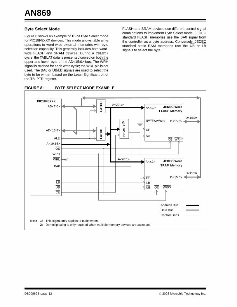
Byte Select Mode
Figure 8 shows an example of 16-bit Byte Select modefor PIC18F8XXX devices. This mode allows table writeoperations to word-wide external memories with byteselection capability. This generally includes both word-wide FLASH and SRAM devices. During a TBLWT*cycle, the TABLAT data is presented copied on both theupper and lower byte of the AD<15:0> bus. The WRHsignal is strobed for each write cycle; the WRL pin is notused. The BA0 or UB/LB signals are used to select thebyte to be written based on the Least Significant bit ofthe TBLPTR register.
FLASH and SRAM devices use different control signalcombinations to implement Byte Select mode. JEDECstandard FLASH memories use the BA0 signal fromthe controller as a byte address. Conversely, JEDECstandard static RAM memories use the UB or LBsignals to select the byte.
FIGURE 8: BYTE SELECT MODE EXAMPLE
AD<7:0>
PIC18F8XXX
AD<15:8>
ALE
LA
TC
HA<20:1>
LA
TC
H
OE
WRH
A<19:16>
WRL
BA0
JEDEC WordA<x:1>
D<15:0>
A<20:1>
CE
D<15:0>
OE WR(1) A0
FLASH Memory
JEDEC WordA<x:1>
D<15:0>CE
D<15:0>
OE WR(1)
LB
UB
SRAM Memory
LB
UB
DE
-MU
X(2
)
Address Bus
Data Bus
Control Lines
Note 1: This signal only applies to table writes.2: Demultiplexing is only required when multiple memory devices are accessed.
CE
BYTE/WORD
DS00869B-page 12 2003 Microchip Technology Inc.

AN869
FIGURE 9: BYTE SELECT MODE TIMING
Q2Q1 Q3 Q4
A<19:16>
ALE
OE
AD<15:0>
TBLWT 36h
Q2Q1 Q3 Q4
01h
8001h
TBLWT A5h
A5A5h
to 030002h to 030003h
BA0
WRH
WRL
01h
UB
LB
8001h 3636h
‘1’
CE ‘0’
‘1’
2003 Microchip Technology Inc. DS00869B-page 13
AN869
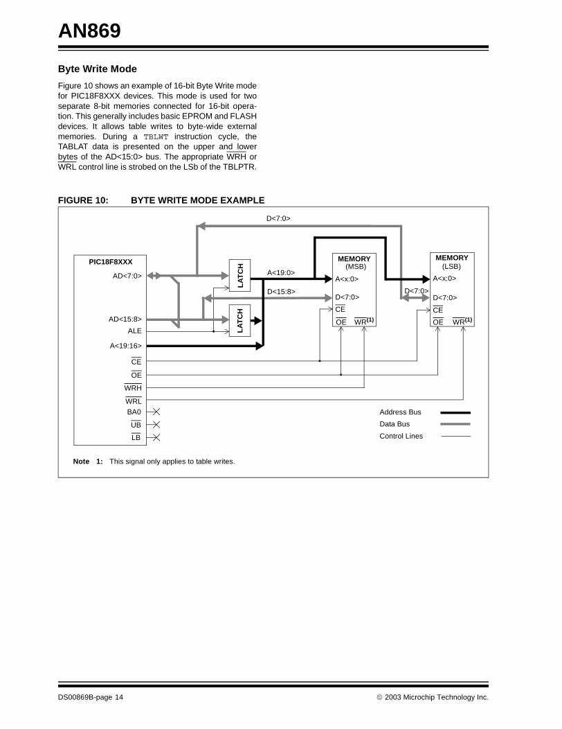
Byte Write Mode
Figure 10 shows an example of 16-bit Byte Write modefor PIC18F8XXX devices. This mode is used for twoseparate 8-bit memories connected for 16-bit opera-tion. This generally includes basic EPROM and FLASHdevices. It allows table writes to byte-wide externalmemories. During a TBLWT instruction cycle, theTABLAT data is presented on the upper and lowerbytes of the AD<15:0> bus. The appropriate WRH orWRL control line is strobed on the LSb of the TBLPTR.
FIGURE 10: BYTE WRITE MODE EXAMPLE
AD<7:0>
A<19:16>
ALE
D<15:8>
LA
TC
H
A<x:0>
D<7:0>
A<19:0>A<x:0>
D<7:0>
LA
TC
H
OE
WRH
OE OEWR(1) WR(1)
CE CE
Note 1: This signal only applies to table writes.
WRL
D<7:0>
(LSB)(MSB)PIC18F8XXX
D<7:0>
AD<15:8>
Address Bus
Data Bus
Control Lines
CE
MEMORYMEMORY
BA0
UB
LB
DS00869B-page 14 2003 Microchip Technology Inc.

AN869
FIGURE 11: BYTE WRITE MODE TIMING
Q2Q1 Q3 Q4
A<19:16>
ALE
OE
AD<15:0>
TBLWT 36h
Q2Q1 Q3 Q4
01h
8001h
TBLWT A5h
A5A5h
to 030002h to 030003h
BA0
WRH
WRL
01h
UB
LB
8001h
CE ‘0’
‘1’
‘1’
3636h
‘1’
‘1’
2003 Microchip Technology Inc. DS00869B-page 15
AN869
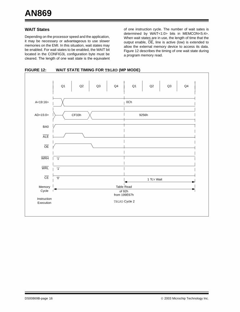
WAIT States
Depending on the processor speed and the application,it may be necessary or advantageous to use slowermemories on the EMI. In this situation, wait states maybe enabled. For wait states to be enabled, the WAIT bitlocated in the CONFIG3L configuration byte must becleared. The length of one wait state is the equivalent
of one instruction cycle. The number of wait sates isdetermined by WAIT<1:0> bits in MEMCON<5:4>.When wait states are in use, the length of time that theoutput enable, OE, line is active (low) is extended toallow the external memory device to access its data.Figure 12 describes the timing of one wait state duringa program memory read.
FIGURE 12: WAIT STATE TIMING FOR TBLRD (MP MODE)
ALE
OE
WRH
WRL
AD<15:0>
BA0
CF33h 9256h
‘1’
‘1’
Table Readof 92h
from 199E67h
1 TCY Wait
A<19:16> 0Ch
CE ‘0’
MemoryCycle
InstructionExecution TBLRD Cycle 2
Q2Q1 Q3 Q4 Q2Q1 Q3 Q4
DS00869B-page 16 2003 Microchip Technology Inc.
AN869
8-BIT EMI SOLUTIONS
Economical 8-Bit Memory Data Storage
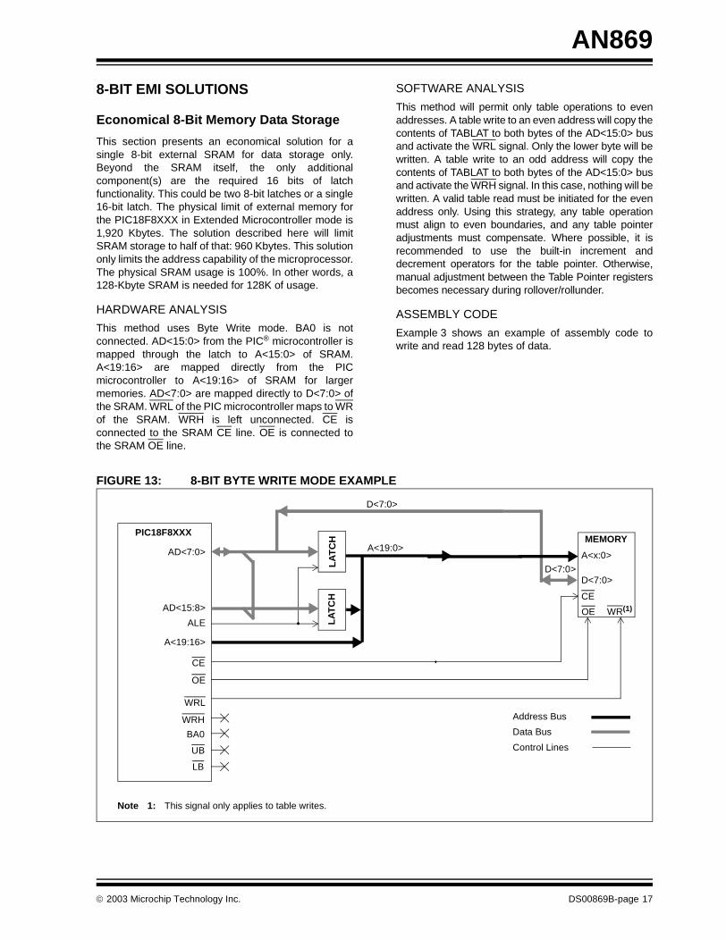
This section presents an economical solution for asingle 8-bit external SRAM for data storage only.Beyond the SRAM itself, the only additionalcomponent(s) are the required 16 bits of latchfunctionality. This could be two 8-bit latches or a single16-bit latch. The physical limit of external memory forthe PIC18F8XXX in Extended Microcontroller mode is1,920 Kbytes. The solution described here will limitSRAM storage to half of that: 960 Kbytes. This solutiononly limits the address capability of the microprocessor.The physical SRAM usage is 100%. In other words, a128-Kbyte SRAM is needed for 128K of usage.
HARDWARE ANALYSIS
This method uses Byte Write mode. BA0 is notconnected. AD<15:0> from the PIC® microcontroller ismapped through the latch to A<15:0> of SRAM.A<19:16> are mapped directly from the PICmicrocontroller to A<19:16> of SRAM for largermemories. AD<7:0> are mapped directly to D<7:0> ofthe SRAM. WRL of the PIC microcontroller maps to WRof the SRAM. WRH is left unconnected. CE isconnected to the SRAM CE line. OE is connected tothe SRAM OE line.
SOFTWARE ANALYSIS
This method will permit only table operations to evenaddresses. A table write to an even address will copy thecontents of TABLAT to both bytes of the AD<15:0> busand activate the WRL signal. Only the lower byte will bewritten. A table write to an odd address will copy thecontents of TABLAT to both bytes of the AD<15:0> busand activate the WRH signal. In this case, nothing will bewritten. A valid table read must be initiated for the evenaddress only. Using this strategy, any table operationmust align to even boundaries, and any table pointeradjustments must compensate. Where possible, it isrecommended to use the built-in increment anddecrement operators for the table pointer. Otherwise,manual adjustment between the Table Pointer registersbecomes necessary during rollover/rollunder.
ASSEMBLY CODE
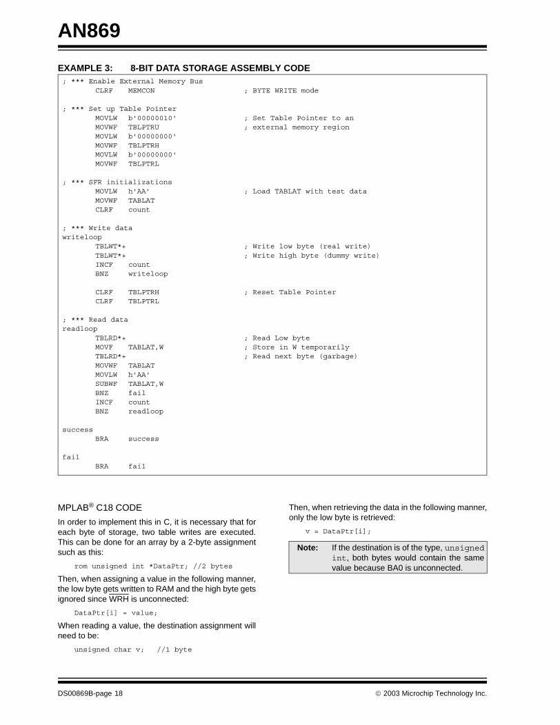
Example 3 shows an example of assembly code towrite and read 128 bytes of data.
FIGURE 13: 8-BIT BYTE WRITE MODE EXAMPLE
AD<7:0>
A<19:16>
ALE
LA
TC
H
A<19:0>A<x:0>
D<7:0>
LA
TC
H
OE
OE WR(1)
CE
Note 1: This signal only applies to table writes.
WRL
D<7:0>
PIC18F8XXX
D<7:0>
AD<15:8>
Address Bus
Data Bus
Control Lines
CE
BA0
UB
LB
WRH
MEMORY
2003 Microchip Technology Inc. DS00869B-page 17
AN869
EXAMPLE 3: 8-BIT DATA STORAGE ASSEMBLY CODE
MPLAB® C18 CODE
In order to implement this in C, it is necessary that foreach byte of storage, two table writes are executed.This can be done for an array by a 2-byte assignmentsuch as this:
rom unsigned int *DataPtr; //2 bytes
Then, when assigning a value in the following manner,the low byte gets written to RAM and the high byte getsignored since WRH is unconnected:
DataPtr[i] = value;
When reading a value, the destination assignment willneed to be:
unsigned char v; //1 byte
Then, when retrieving the data in the following manner,only the low byte is retrieved:
v = DataPtr[i];
; *** Enable External Memory BusCLRF MEMCON ; BYTE WRITE mode
; *** Set up Table PointerMOVLW b'00000010' ; Set Table Pointer to an MOVWF TBLPTRU ; external memory regionMOVLW b'00000000'MOVWF TBLPTRHMOVLW b'00000000'MOVWF TBLPTRL
; *** SFR initializationsMOVLW h'AA’ ; Load TABLAT with test dataMOVWF TABLATCLRF count
; *** Write datawriteloop
TBLWT*+ ; Write low byte (real write)TBLWT*+ ; Write high byte (dummy write)INCF countBNZ writeloop
CLRF TBLPTRH ; Reset Table PointerCLRF TBLPTRL
; *** Read datareadloop
TBLRD*+ ; Read Low byteMOVF TABLAT,W ; Store in W temporarilyTBLRD*+ ; Read next byte (garbage)MOVWF TABLATMOVLW h'AA'SUBWF TABLAT,WBNZ failINCF countBNZ readloop
successBRA success
failBRA fail
Note: If the destination is of the type, unsignedint, both bytes would contain the samevalue because BA0 is unconnected.
DS00869B-page 18 2003 Microchip Technology Inc.
AN869
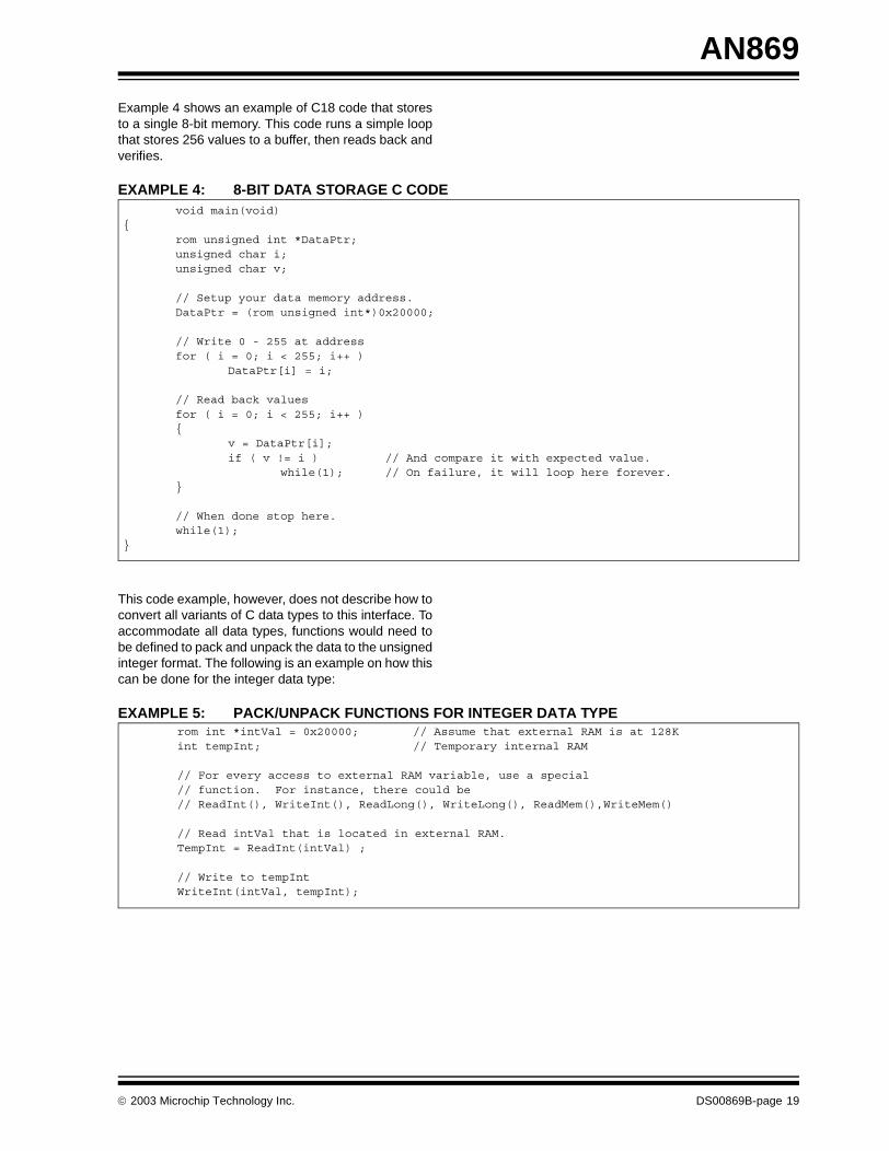
Example 4 shows an example of C18 code that storesto a single 8-bit memory. This code runs a simple loopthat stores 256 values to a buffer, then reads back andverifies.
EXAMPLE 4: 8-BIT DATA STORAGE C CODE
This code example, however, does not describe how toconvert all variants of C data types to this interface. Toaccommodate all data types, functions would need tobe defined to pack and unpack the data to the unsignedinteger format. The following is an example on how thiscan be done for the integer data type:
EXAMPLE 5: PACK/UNPACK FUNCTIONS FOR INTEGER DATA TYPE
void main(void){
rom unsigned int *DataPtr;unsigned char i;unsigned char v;
// Setup your data memory address.DataPtr = (rom unsigned int*)0x20000;
// Write 0 - 255 at address for ( i = 0; i < 255; i++ )
DataPtr[i] = i;
// Read back values for ( i = 0; i < 255; i++ ){
v = DataPtr[i];if ( v != i ) // And compare it with expected value.
while(1); // On failure, it will loop here forever.}
// When done stop here.while(1);
}
rom int *intVal = 0x20000; // Assume that external RAM is at 128Kint tempInt; // Temporary internal RAM
// For every access to external RAM variable, use a special // function. For instance, there could be// ReadInt(), WriteInt(), ReadLong(), WriteLong(), ReadMem(),WriteMem()
// Read intVal that is located in external RAM.TempInt = ReadInt(intVal) ;
// Write to tempIntWriteInt(intVal, tempInt);
2003 Microchip Technology Inc. DS00869B-page 19
AN869
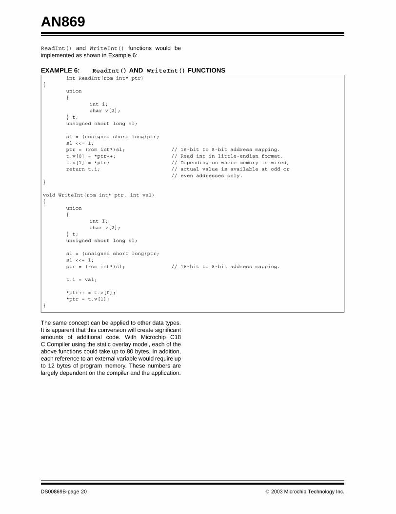
ReadInt() and WriteInt() functions would beimplemented as shown in Example 6:
EXAMPLE 6: ReadInt() AND WriteInt() FUNCTIONS
The same concept can be applied to other data types.It is apparent that this conversion will create significantamounts of additional code. With Microchip C18C Compiler using the static overlay model, each of theabove functions could take up to 80 bytes. In addition,each reference to an external variable would require upto 12 bytes of program memory. These numbers arelargely dependent on the compiler and the application.
int ReadInt(rom int* ptr){
union{
int i;char v[2];
} t;unsigned short long sl;
sl = (unsigned short long)ptr;sl <<= 1;ptr = (rom int*)sl; // 16-bit to 8-bit address mapping.t.v[0] = *ptr++; // Read int in little-endian format.t.v[1] = *ptr; // Depending on where memory is wired,return t.i; // actual value is available at odd or
// even addresses only.}
void WriteInt(rom int* ptr, int val){
union{
int I;char v[2];
} t;unsigned short long sl;
sl = (unsigned short long)ptr;sl <<= 1;ptr = (rom int*)sl; // 16-bit to 8-bit address mapping.
t.i = val;
*ptr++ = t.v[0];*ptr = t.v[1];
}
DS00869B-page 20 2003 Microchip Technology Inc.
AN869
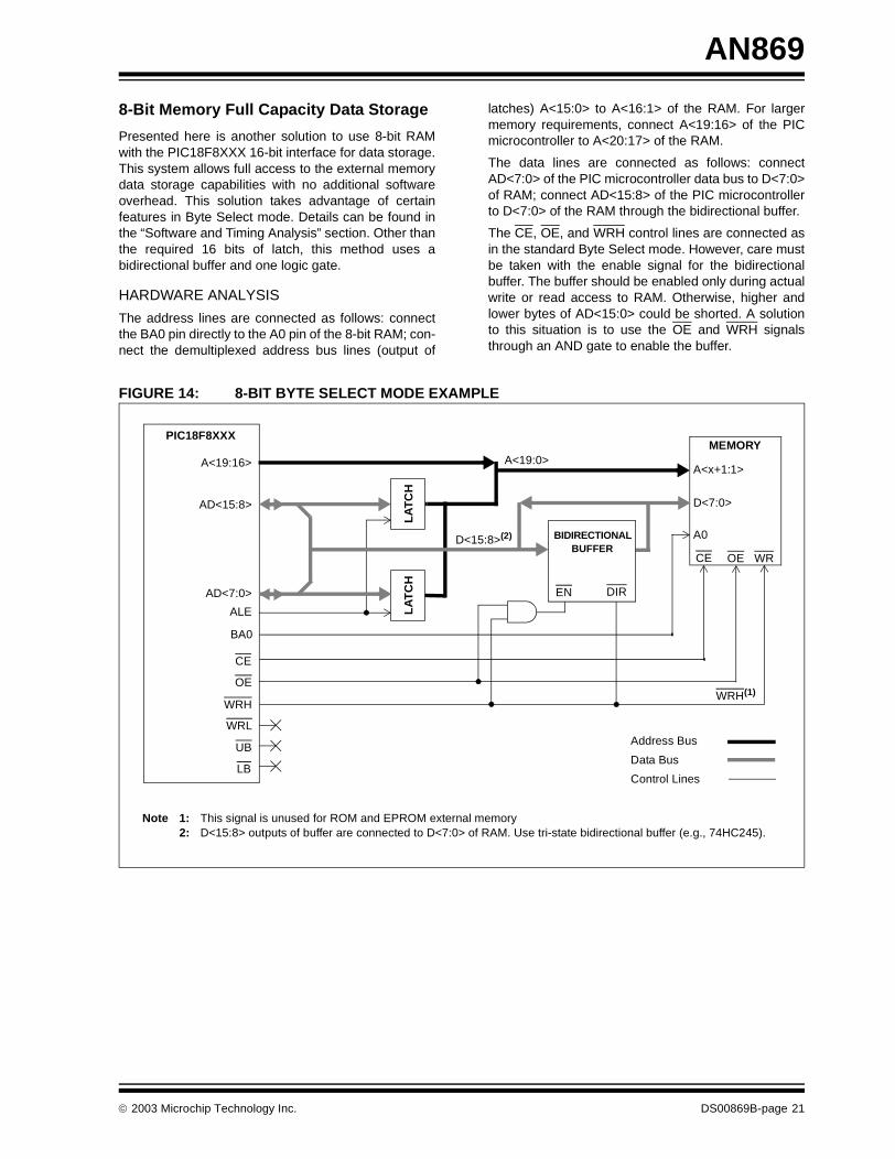
8-Bit Memory Full Capacity Data Storage
Presented here is another solution to use 8-bit RAMwith the PIC18F8XXX 16-bit interface for data storage.This system allows full access to the external memorydata storage capabilities with no additional softwareoverhead. This solution takes advantage of certainfeatures in Byte Select mode. Details can be found inthe “Software and Timing Analysis” section. Other thanthe required 16 bits of latch, this method uses abidirectional buffer and one logic gate.
HARDWARE ANALYSIS
The address lines are connected as follows: connectthe BA0 pin directly to the A0 pin of the 8-bit RAM; con-nect the demultiplexed address bus lines (output of
latches) A<15:0> to A<16:1> of the RAM. For largermemory requirements, connect A<19:16> of the PICmicrocontroller to A<20:17> of the RAM.
The data lines are connected as follows: connectAD<7:0> of the PIC microcontroller data bus to D<7:0>of RAM; connect AD<15:8> of the PIC microcontrollerto D<7:0> of the RAM through the bidirectional buffer.
The CE, OE, and WRH control lines are connected asin the standard Byte Select mode. However, care mustbe taken with the enable signal for the bidirectionalbuffer. The buffer should be enabled only during actualwrite or read access to RAM. Otherwise, higher andlower bytes of AD<15:0> could be shorted. A solutionto this situation is to use the OE and WRH signalsthrough an AND gate to enable the buffer.
FIGURE 14: 8-BIT BYTE SELECT MODE EXAMPLE
AD<15:8>
ALE
LA
TC
H
A<x+1:1>
D<7:0>
LA
TC
H
OE
WRH
OE WR
A0
Note 1: This signal is unused for ROM and EPROM external memory2: D<15:8> outputs of buffer are connected to D<7:0> of RAM. Use tri-state bidirectional buffer (e.g., 74HC245).
UB
AD<7:0>
Address Bus
Data Bus
Control Lines
CE
BA0
A<19:16>
CE
MEMORYA<19:0>
D<15:8>(2)
WRH(1)
PIC18F8XXX
WRL
LB
BUFFER
EN DIR
BIDIRECTIONAL
2003 Microchip Technology Inc. DS00869B-page 21
AN869
SOFTWARE AND TIMING ANALYSIS
Data storage is accessed with TBLRD* and TBLWT*instructions in standard fashion. The function of tablewrites in Byte Select mode is critical for this solution.The following is a discussion of the signal timings in thissolution for both operations. Please refer to Figure 5 forthe table read timings and Figure 9 for the table writetimings.
TBLRD cycle 2 shows when the actual read occurs.During Q1 and Q2, the address is placed on the AD busand the use of the ALE signal latches the address. TheBA0 is active during Q1 to Q4, providing demultiplexedA0 address bit for the RAM. The use of the OE signaldisables the buffer during this access, allowing proper16-bit address to latch. During Q3 and Q4, the OEsignal is activated; this enables the buffer which copiesthe RAM data on D<7:0> to D<15:8>. Now, dependingon the status of BA0 (odd or even address), the PICmicrocontroller will copy the data of LSB or MSB toTABLAT. As LSB and MSB contain the same data,TABLAT will contain the proper value for any address.
TBLWT cycle 2 shows when the actual write occurs.During Q1 and Q2, the address is placed on the AD busand the use of the ALE signal latches the address. TheBA0 is active during Q1 to Q4, providing demultiplexedA0 address bit for RAM. The use of the WRH signal dis-ables the buffer during this access, allowing the proper16-bit address to latch. During Q3 and Q4, the WRHsignal is activated; this enables the buffer which copiesthe RAM data on D<15:8> to D<7:0>. This may appearto be a problem as D<15:8> and D<7:0> are shortedthrough buffer. However, it is not because of ByteSelect mode. In this mode, the PIC microcontrollerwrites the same data to LSB and MSB. Therefore,D<15:8> and D<7:0> contain the same data irrespec-tive to the address being written. Therefore, input dataof RAM remains the same even after this indirect short.
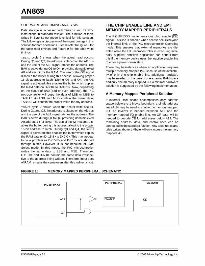
THE CHIP ENABLE LINE AND EMI MEMORY MAPPED PERIPHERALS
The PIC18F8XXX implements one chip enable (CE)signal. This line is enabled when access occurs beyondthe internal limit of the PIC microcontroller Operatingmode. This ensures that external memories are dis-abled while the PIC microcontroller is executing inter-nally. A power sensitive application can benefit fromthis if the memory device uses the inactive enable lineto enter a power-down state.
There may be instances where an application requiresmultiple memory mapped I/O. Because of the availabil-ity of only one chip enable line, additional hardwaremay be needed. In the case of one external RAM spaceand only one memory mapped I/O, a minimal hardwaresolution is suggested by the following implementation.
A Memory Mapped Peripheral Solution
If external RAM space encompasses only addressspace below the 1-Mbyte boundary, a single addressline (A19) may be used to enable the memory mappedI/O. An inverter is needed between A19 and thememory mapped I/O enable line. An OR gate will beneeded to decode CE for addresses below A19. Theremaining address, data, and control lines can beconnected in the standard fashion. Any table reads andtable writes above 1 Mbyte will only access the memorymapped I/O.
FIGURE 15: MEMORY MAPPED PERIPHERAL SCHEMATIC
ENABLE
PERIPHERAL MEMORY
CE
CE
A19
PIC18F8XXX
DS00869B-page 22 2003 Microchip Technology Inc.
AN869
SUMMARY
The PIC18F8XXX family greatly enhances the capabil-ity of any application through access to externaldevices. Large amounts of code and data storagebecome available using the External Memory Interface.With minimal amounts of effort and cost, most any 8-bitor 16-bit memory device can complement your PICmicrocontroller based application.
2003 Microchip Technology Inc. DS00869B-page 23
AN869
NOTES:
DS00869B-page 24 2003 Microchip Technology Inc.
Note the following details of the code protection feature on Microchip devices:
• Microchip products meet the specification contained in their particular Microchip Data Sheet.
• Microchip believes that its family of products is one of the most secure families of its kind on the market today, when used in the intended manner and under normal conditions.
• There are dishonest and possibly illegal methods used to breach the code protection feature. All of these methods, to our knowledge, require using the Microchip products in a manner outside the operating specifications contained in Microchip's Data Sheets. Most likely, the person doing so is engaged in theft of intellectual property.
• Microchip is willing to work with the customer who is concerned about the integrity of their code.
• Neither Microchip nor any other semiconductor manufacturer can guarantee the security of their code. Code protection does not mean that we are guaranteeing the product as “unbreakable.”
Code protection is constantly evolving. We at Microchip are committed to continuously improving the code protection features of ourproducts. Attempts to break microchip’s code protection feature may be a violation of the Digital Millennium Copyright Act. If such actsallow unauthorized access to your software or other copyrighted work, you may have a right to sue for relief under that Act.
Information contained in this publication regarding deviceapplications and the like is intended through suggestion onlyand may be superseded by updates. It is your responsibility toensure that your application meets with your specifications.No representation or warranty is given and no liability isassumed by Microchip Technology Incorporated with respectto the accuracy or use of such information, or infringement ofpatents or other intellectual property rights arising from suchuse or otherwise. Use of Microchip’s products as criticalcomponents in life support systems is not authorized exceptwith express written approval by Microchip. No licenses areconveyed, implicitly or otherwise, under any intellectualproperty rights.
2003 Microchip Technology Inc.
Trademarks
The Microchip name and logo, the Microchip logo, dsPIC, KEELOQ, MPLAB, PIC, PICmicro, PICSTART, PRO MATE and PowerSmart are registered trademarks of Microchip Technology Incorporated in the U.S.A. and other countries.
FilterLab, microID, MXDEV, MXLAB, PICMASTER, SEEVAL and The Embedded Control Solutions Company are registered trademarks of Microchip Technology Incorporated in the U.S.A.
Accuron, Application Maestro, dsPICDEM, dsPICDEM.net, ECONOMONITOR, FanSense, FlexROM, fuzzyLAB, In-Circuit Serial Programming, ICSP, ICEPIC, microPort, Migratable Memory, MPASM, MPLIB, MPLINK, MPSIM, PICC, PICkit, PICDEM, PICDEM.net, PowerCal, PowerInfo, PowerMate, PowerTool, rfLAB, rfPIC, Select Mode, SmartSensor, SmartShunt, SmartTel and Total Endurance are trademarks of Microchip Technology Incorporated in the U.S.A. and other countries.
Serialized Quick Turn Programming (SQTP) is a service markof Microchip Technology Incorporated in the U.S.A.
All other trademarks mentioned herein are property of theirrespective companies.
© 2003, Microchip Technology Incorporated, Printed in theU.S.A., All Rights Reserved.
Printed on recycled paper.
DS00869B-page 25
Microchip received QS-9000 quality system certification for its worldwide headquarters, design and wafer fabrication facilities in Chandler and Tempe, Arizona in July 1999 and Mountain View, California in March 2002. The Company’s quality system processes and procedures are QS-9000 compliant for its PICmicro® 8-bit MCUs, KEELOQ® code hopping devices, Serial EEPROMs, microperipherals, non-volatile memory and analog products. In addition, Microchip’s quality system for the design and manufacture of development systems is ISO 9001 certified.
DS00869B-page 26 2003 Microchip Technology Inc.
AMERICASCorporate Office2355 West Chandler Blvd.Chandler, AZ 85224-6199Tel: 480-792-7200 Fax: 480-792-7277Technical Support: 480-792-7627Web Address: http://www.microchip.com
Atlanta3780 Mansell Road, Suite 130Alpharetta, GA 30022Tel: 770-640-0034 Fax: 770-640-0307
Boston2 Lan Drive, Suite 120Westford, MA 01886Tel: 978-692-3848 Fax: 978-692-3821
Chicago333 Pierce Road, Suite 180Itasca, IL 60143Tel: 630-285-0071 Fax: 630-285-0075
Dallas4570 Westgrove Drive, Suite 160Addison, TX 75001Tel: 972-818-7423 Fax: 972-818-2924
DetroitTri-Atria Office Building 32255 Northwestern Highway, Suite 190Farmington Hills, MI 48334Tel: 248-538-2250 Fax: 248-538-2260
Kokomo2767 S. Albright Road Kokomo, IN 46902Tel: 765-864-8360 Fax: 765-864-8387
Los Angeles18201 Von Karman, Suite 1090Irvine, CA 92612Tel: 949-263-1888 Fax: 949-263-1338
Phoenix2355 West Chandler Blvd.Chandler, AZ 85224-6199Tel: 480-792-7966 Fax: 480-792-4338
San JoseMicrochip Technology Inc.2107 North First Street, Suite 590San Jose, CA 95131Tel: 408-436-7950 Fax: 408-436-7955
Toronto6285 Northam Drive, Suite 108Mississauga, Ontario L4V 1X5, CanadaTel: 905-673-0699 Fax: 905-673-6509
ASIA/PACIFICAustraliaMicrochip Technology Australia Pty LtdMarketing Support DivisionSuite 22, 41 Rawson StreetEpping 2121, NSWAustraliaTel: 61-2-9868-6733 Fax: 61-2-9868-6755
China - BeijingMicrochip Technology Consulting (Shanghai)Co., Ltd., Beijing Liaison OfficeUnit 915Bei Hai Wan Tai Bldg.No. 6 Chaoyangmen Beidajie Beijing, 100027, No. ChinaTel: 86-10-85282100 Fax: 86-10-85282104China - ChengduMicrochip Technology Consulting (Shanghai)Co., Ltd., Chengdu Liaison OfficeRm. 2401-2402, 24th Floor, Ming Xing Financial TowerNo. 88 TIDU StreetChengdu 610016, ChinaTel: 86-28-86766200 Fax: 86-28-86766599China - FuzhouMicrochip Technology Consulting (Shanghai)Co., Ltd., Fuzhou Liaison OfficeUnit 28F, World Trade PlazaNo. 71 Wusi RoadFuzhou 350001, ChinaTel: 86-591-7503506 Fax: 86-591-7503521China - Hong Kong SARMicrochip Technology Hongkong Ltd.Unit 901-6, Tower 2, Metroplaza223 Hing Fong RoadKwai Fong, N.T., Hong KongTel: 852-2401-1200 Fax: 852-2401-3431China - ShanghaiMicrochip Technology Consulting (Shanghai)Co., Ltd.Room 701, Bldg. BFar East International PlazaNo. 317 Xian Xia RoadShanghai, 200051Tel: 86-21-6275-5700 Fax: 86-21-6275-5060China - ShenzhenMicrochip Technology Consulting (Shanghai)Co., Ltd., Shenzhen Liaison OfficeRm. 1812, 18/F, Building A, United PlazaNo. 5022 Binhe Road, Futian DistrictShenzhen 518033, ChinaTel: 86-755-82901380 Fax: 86-755-8295-1393China - QingdaoRm. B505A, Fullhope Plaza,No. 12 Hong Kong Central Rd.Qingdao 266071, ChinaTel: 86-532-5027355 Fax: 86-532-5027205IndiaMicrochip Technology Inc.India Liaison OfficeMarketing Support DivisionDivyasree Chambers1 Floor, Wing A (A3/A4)No. 11, O’Shaugnessey RoadBangalore, 560 025, IndiaTel: 91-80-2290061 Fax: 91-80-2290062JapanMicrochip Technology Japan K.K.Benex S-1 6F3-18-20, ShinyokohamaKohoku-Ku, Yokohama-shiKanagawa, 222-0033, JapanTel: 81-45-471- 6166 Fax: 81-45-471-6122
KoreaMicrochip Technology Korea168-1, Youngbo Bldg. 3 FloorSamsung-Dong, Kangnam-KuSeoul, Korea 135-882Tel: 82-2-554-7200 Fax: 82-2-558-5932 or 82-2-558-5934SingaporeMicrochip Technology Singapore Pte Ltd.200 Middle Road#07-02 Prime CentreSingapore, 188980Tel: 65-6334-8870 Fax: 65-6334-8850TaiwanMicrochip Technology (Barbados) Inc., Taiwan Branch11F-3, No. 207Tung Hua North RoadTaipei, 105, TaiwanTel: 886-2-2717-7175 Fax: 886-2-2545-0139
EUROPEAustriaMicrochip Technology Austria GmbHDurisolstrasse 2A-4600 WelsAustriaTel: 43-7242-2244-399Fax: 43-7242-2244-393DenmarkMicrochip Technology Nordic ApSRegus Business CentreLautrup hoj 1-3Ballerup DK-2750 DenmarkTel: 45-4420-9895 Fax: 45-4420-9910FranceMicrochip Technology SARLParc d’Activite du Moulin de Massy43 Rue du Saule TrapuBatiment A - ler Etage91300 Massy, FranceTel: 33-1-69-53-63-20 Fax: 33-1-69-30-90-79GermanyMicrochip Technology GmbHSteinheilstrasse 10D-85737 Ismaning, GermanyTel: 49-89-627-144-0 Fax: 49-89-627-144-44ItalyMicrochip Technology SRLVia Quasimodo, 1220025 Legnano (MI)Milan, Italy Tel: 39-0331-742611 Fax: 39-0331-466781NetherlandsMicrochip Technology NetherlandsP. A. De Biesbosch 14NL-5152 SC Drunen, NetherlandsTel: 31-416-690399 Fax: 31-416-690340United KingdomMicrochip Ltd.505 Eskdale RoadWinnersh TriangleWokingham Berkshire, England RG41 5TUTel: 44-118-921-5869 Fax: 44-118-921-5820
07/10/03
WORLDWIDE SALES AND SERVICE