Embed Size (px)
DESCRIPTION
User Manual for the ANACOM 2 module
Citation preview
AT02 The ANACOM 2 BoardStudent Workbook Chapter 6
Chapter 6The ANACOM 2 Board
LJ Technical Systems 85
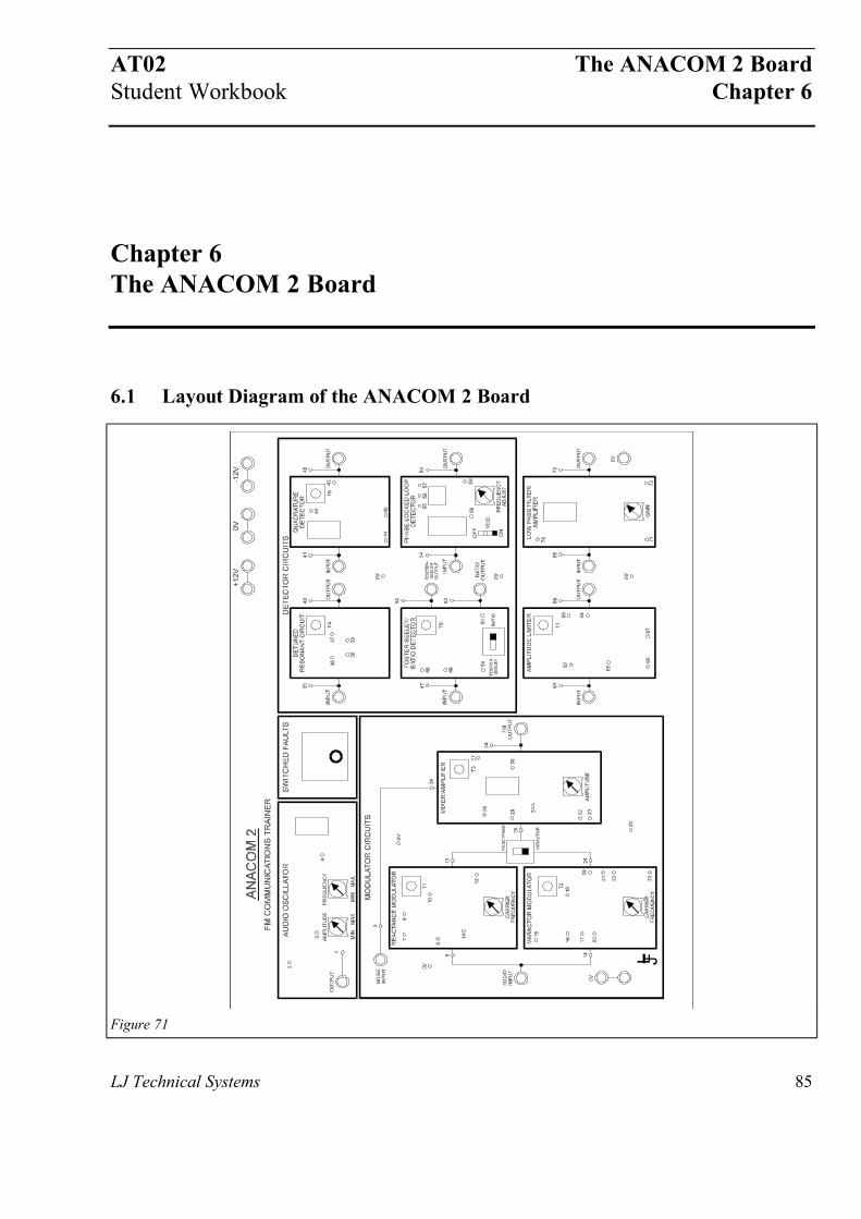
6.1 Layout Diagram of the ANACOM 2 Board
Figure 71
The ANACOM 2 Board AT02Chapter 6 Student Workbook
86 LJ Technical Systems
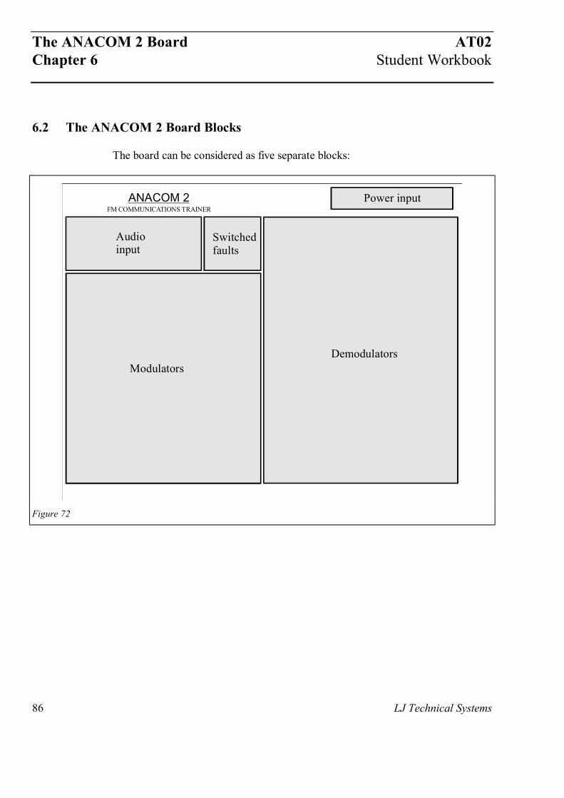
6.2 The ANACOM 2 Board Blocks
The board can be considered as five separate blocks:
ANACOM 2FM COMMUNICATIONS TRAINER
Switchedfaults
Audioinput
ModulatorsDemodulators
Power input
Figure 72
AT02 The ANACOM 2 BoardStudent Workbook Chapter 6
LJ Technical Systems 87
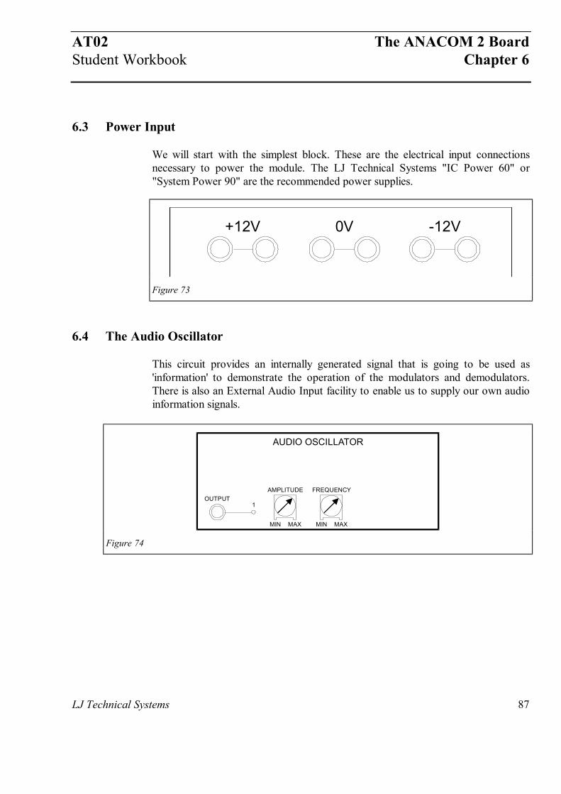
6.3 Power Input
We will start with the simplest block. These are the electrical input connectionsnecessary to power the module. The LJ Technical Systems "IC Power 60" or"System Power 90" are the recommended power supplies.
+12V -12V0V
Figure 73
6.4 The Audio Oscillator
This circuit provides an internally generated signal that is going to be used as'information' to demonstrate the operation of the modulators and demodulators.There is also an External Audio Input facility to enable us to supply our own audioinformation signals.
1OUTPUT
MIN MINMAX MAX
AMPLITUDE FREQUENCY
AUDIO OSCILLATOR
Figure 74
The ANACOM 2 Board AT02Chapter 6 Student Workbook
88 LJ Technical Systems
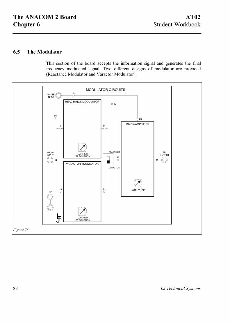
6.5 The Modulator
This section of the board accepts the information signal and generates the finalfrequency modulated signal. Two different designs of modulator are provided(Reactance Modulator and Varactor Modulator).
MODULATOR CIRCUITS
VARACTOR MODULATOR
REACTANCE MODULATOR
MIXER/AMPLIFIER
5
0V
AMPLITUDE
25
14 240V
REACTANCE
VARACTOR
6 13
260V
NOISEINPUT
AUDIOINPUT CARRIER
FREQUENCY
CARRIERFREQUENCY
LJ
FMOUTPUT
Figure 75
AT02 The ANACOM 2 BoardStudent Workbook Chapter 6
LJ Technical Systems 89
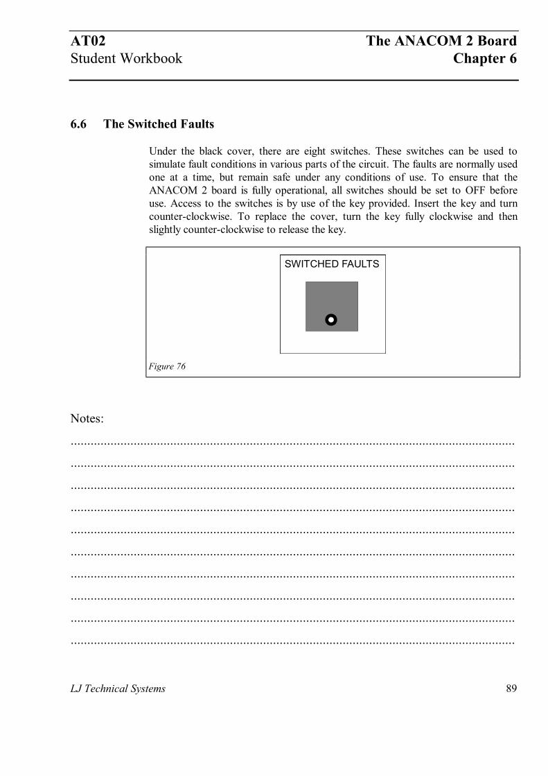
6.6 The Switched Faults
Under the black cover, there are eight switches. These switches can be used tosimulate fault conditions in various parts of the circuit. The faults are normally usedone at a time, but remain safe under any conditions of use. To ensure that theANACOM 2 board is fully operational, all switches should be set to OFF beforeuse. Access to the switches is by use of the key provided. Insert the key and turncounter-clockwise. To replace the cover, turn the key fully clockwise and thenslightly counter-clockwise to release the key.
SWITCHED FAULTS
Figure 76
Notes:
......................................................................................................................................
......................................................................................................................................
......................................................................................................................................
......................................................................................................................................
......................................................................................................................................
......................................................................................................................................
......................................................................................................................................
......................................................................................................................................
......................................................................................................................................
......................................................................................................................................
The ANACOM 2 Board AT02Chapter 6 Student Workbook
90 LJ Technical Systems
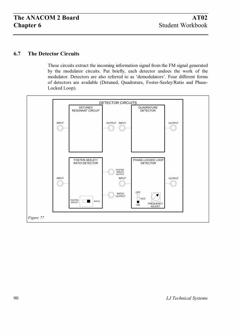
6.7 The Detector Circuits
These circuits extract the incoming information signal from the FM signal generatedby the modulator circuits. Put briefly, each detector undoes the work of themodulator. Detectors are also referred to as ‘demodulators’. Four different formsof detectors are available (Detuned, Quadrature, Foster-Seeley/Ratio and Phase-Locked Loop).
PHASE-LOCKED LOOPDETECTOR
FOSTER-SEELEY/RATIO DETECTOR
QUADRATUREDETECTOR
DETUNEDRESONANT CIRCUIT
DETECTOR CIRCUITS
OFF
ON
VCO
INPUT
INPUT INPUT
RATIOOUTPUT
FREQUENCYADJUST
INPUTOUTPUT OUTPUT
OUTPUT
FOSTER-SEELEY
FOSTER-SEELEYOUTPUT
RATIO
Figure 77
AT02 The ANACOM 2 BoardStudent Workbook Chapter 6
LJ Technical Systems 91
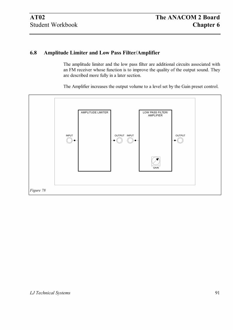
6.8 Amplitude Limiter and Low Pass Filter/Amplifier
The amplitude limiter and the low pass filter are additional circuits associated withan FM receiver whose function is to improve the quality of the output sound. Theyare described more fully in a later section.
The Amplifier increases the output volume to a level set by the Gain preset control.
AMPLITUDE LIMITER LOW PASS FILTER/AMPLIFIER
INPUT INPUTOUTPUT
GAIN
OUTPUT
Figure 78
The ANACOM 2 Board AT02Chapter 6 Student Workbook
92 LJ Technical Systems
Notes:
.....................................................................................................................................
.....................................................................................................................................
.....................................................................................................................................
.....................................................................................................................................
.....................................................................................................................................
.....................................................................................................................................
.....................................................................................................................................
.....................................................................................................................................
.....................................................................................................................................
.....................................................................................................................................
.....................................................................................................................................
.....................................................................................................................................
.....................................................................................................................................
.....................................................................................................................................
.....................................................................................................................................
.....................................................................................................................................
.....................................................................................................................................
.....................................................................................................................................
.....................................................................................................................................
.....................................................................................................................................
.....................................................................................................................................
.....................................................................................................................................
.....................................................................................................................................
AT02 FM ModulatorsStudent Workbook Chapter 7
Chapter 7FM Modulators
LJ Technical Systems 93
7.1 Frequency Modulation (FM)
As we saw in Section 2.5, one method of combining an information signal with acarrier wave was by amplitude modulation. In that case, we used the informationsignal to vary the amplitude of the carrier wave and then, at the receiver, thesevariations in the amplitude were detected and the information recovered.
An alternative system is frequency modulation in which the information signal isused to control the frequency of the carrier wave. This works equally well, and insome respects, better than amplitude modulation.
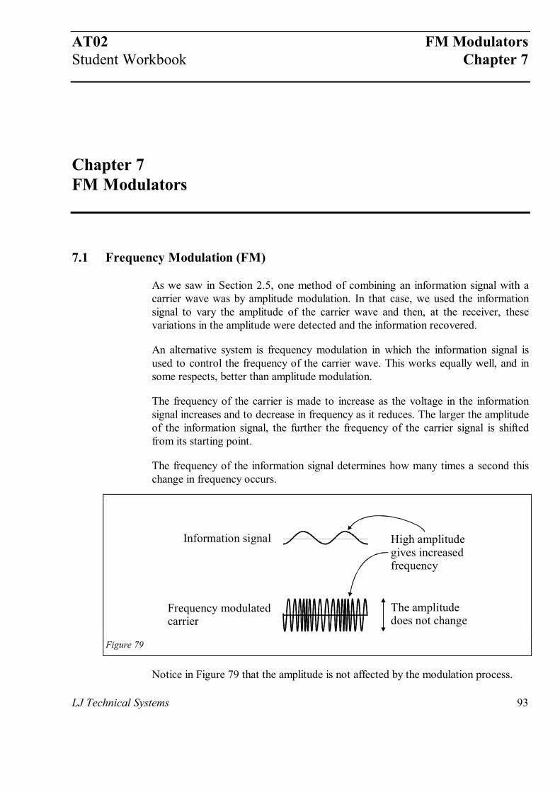
The frequency of the carrier is made to increase as the voltage in the informationsignal increases and to decrease in frequency as it reduces. The larger the amplitudeof the information signal, the further the frequency of the carrier signal is shiftedfrom its starting point.
The frequency of the information signal determines how many times a second thischange in frequency occurs.
Information signal
Frequency modulatedcarrier
The amplitudedoes not change
High amplitudegives increasedfrequency
Figure 79
Notice in Figure 79 that the amplitude is not affected by the modulation process.
FM Modulators AT02Chapter 7 Student Workbook
94 LJ Technical Systems
7.2 Frequency Deviation
How much the frequency is changed for each volt of information signal is called the‘Frequency Deviation’ and a typical value is 15kHz/V with an upper limit of±75kHz
As an example, an information signal of peak-to-peak voltage of 6 volts and afrequency of 10kHz with a frequency deviation of 15kHz/V would cause an FMcarrier to change by a total of 90kHz (45kHz above and below the original carrierfrequency). The carrier frequency would be swept over this range 10,000 times asecond.
7.3 The Advantages of FM
There are three advantages of frequency modulation for a communication system.
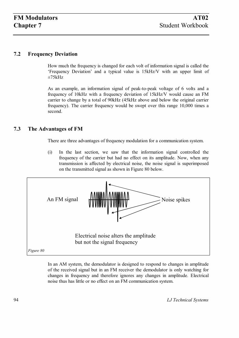
(i) In the last section, we saw that the information signal controlled thefrequency of the carrier but had no effect on its amplitude. Now, when anytransmission is affected by electrical noise, the noise signal is superimposedon the transmitted signal as shown in Figure 80 below.
Electrical noise alters the amplitudebut not the signal frequency
Noise spikesAn FM signal
Figure 80
In an AM system, the demodulator is designed to respond to changes in amplitudeof the received signal but in an FM receiver the demodulator is only watching forchanges in frequency and therefore ignores any changes in amplitude. Electricalnoise thus has little or no effect on an FM communication system.
AT02 FM ModulatorsStudent Workbook Chapter 7
LJ Technical Systems 95
(ii) The bandwidth of the FM signal is very wide compared with an AMtransmission. Typical broadcast bandwidths are in the order of 250kHz. Thisallows a much better sound quality, so signals like music sound significantlybetter if frequency modulation is being used.
(iii) When an FM demodulator is receiving an FM signal, it follows the variationsin frequency of the incoming signal and is said to ‘lock on’ to the receivedtransmission. This has a great advantage when two transmissions are receivedat the same time. The receiver ‘locks on’ to the stronger of the two signalsand ignores the other. This is called the ‘capture effect’ and it means that wecan listen to an FM station on a radio without interference from otherstations.
7.4 The Disadvantage of FM
This is the wide bandwidth of the transmission.
The medium frequency broadcast band extends from about 550kHz to 1,600kHz,and is therefore only a little over 1MHz in width. If we tried to use FM using abandwidth of 250kHz for each station, it would mean that no more than fourstations could be accommodated. This wide bandwidth forces us to use highercarrier frequencies, usually in the VHF band that extends from about 85MHz to110MHz. This is a width of 25MHz and would hold many more stations.
7.5 The Bandwidth of an FM Signal
The frequency modulation process generates a large number of side frequencies.Theoretically, the sidebands are infinitely wide with the power levels becominglower and lower as we move away from the carrier frequency. The bandwidth of250kHz was chosen as a convenient value to ensure a low value of distortion in thereceived signal whilst allowing many stations to be accommodated in the VHFbroadcast band. Communication signals that do not require the high qualityassociated with broadcast stations can adopt a narrower bandwidth to enable moretransmissions within their allotted frequency band. Marine communications for shipto ship communications, for example, use a bandwidth of only 25kHz but this isonly for speech and the quality is not important.
These bandwidth figures bear no easy relationship with the frequency of theinformation signal nor with the frequency deviation - or, it seems, anything else. FMis unlike AM in this respect.
FM Modulators AT02Chapter 7 Student Workbook
96 LJ Technical Systems
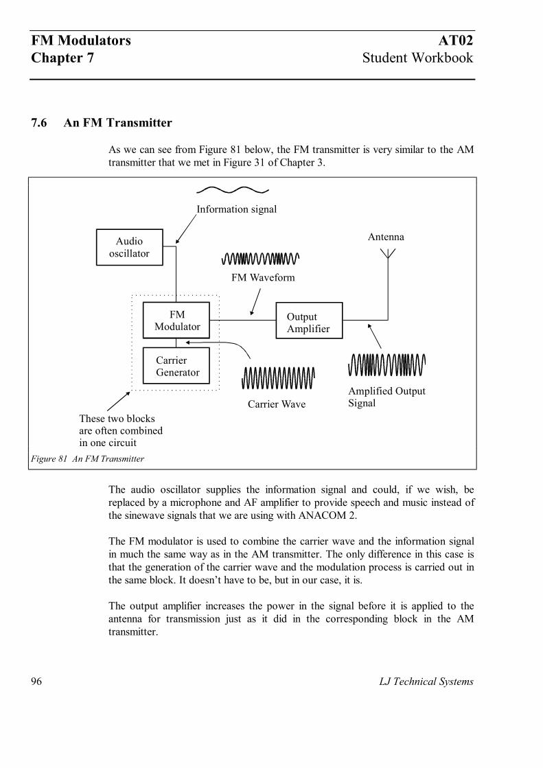
7.6 An FM Transmitter
As we can see from Figure 81 below, the FM transmitter is very similar to the AMtransmitter that we met in Figure 31 of Chapter 3.
Audiooscillator
FMModulator
OutputAmplifier
CarrierGenerator
Antenna
Information signal
Carrier Wave
FM Waveform
Amplified OutputSignal
These two blocksare often combinedin one circuit
Figure 81 An FM Transmitter
The audio oscillator supplies the information signal and could, if we wish, bereplaced by a microphone and AF amplifier to provide speech and music instead ofthe sinewave signals that we are using with ANACOM 2.
The FM modulator is used to combine the carrier wave and the information signalin much the same way as in the AM transmitter. The only difference in this case isthat the generation of the carrier wave and the modulation process is carried out inthe same block. It doesn’t have to be, but in our case, it is.
The output amplifier increases the power in the signal before it is applied to theantenna for transmission just as it did in the corresponding block in the AMtransmitter.
AT02 FM ModulatorsStudent Workbook Chapter 7
LJ Technical Systems 97
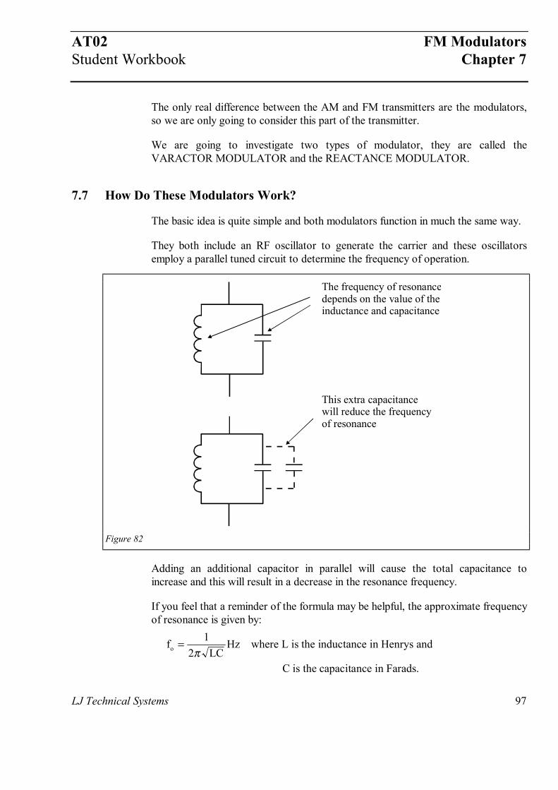
The only real difference between the AM and FM transmitters are the modulators,so we are only going to consider this part of the transmitter.
We are going to investigate two types of modulator, they are called theVARACTOR MODULATOR and the REACTANCE MODULATOR.
7.7 How Do These Modulators Work?
The basic idea is quite simple and both modulators function in much the same way.
They both include an RF oscillator to generate the carrier and these oscillatorsemploy a parallel tuned circuit to determine the frequency of operation.
This extra capacitancewill reduce the frequencyof resonance
The frequency of resonancedepends on the value of theinductance and capacitance
Figure 82
Adding an additional capacitor in parallel will cause the total capacitance toincrease and this will result in a decrease in the resonance frequency.
If you feel that a reminder of the formula may be helpful, the approximate frequencyof resonance is given by:
fLC
Hz whero = 12π
e L is the inductance in Henrys and
C is the capacitance in Farads.
FM Modulators AT02Chapter 7 Student Workbook
98 LJ Technical Systems
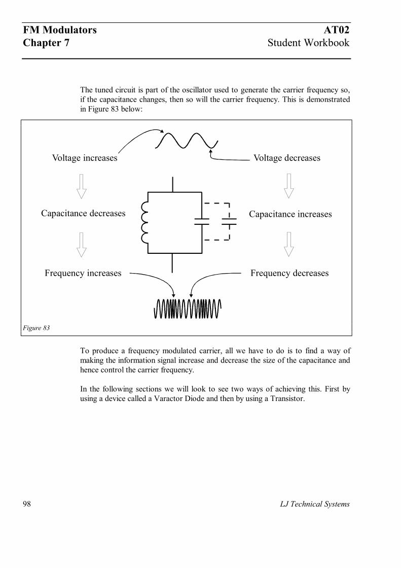
The tuned circuit is part of the oscillator used to generate the carrier frequency so,if the capacitance changes, then so will the carrier frequency. This is demonstratedin Figure 83 below:
Voltage increases
Capacitance increases
Voltage decreases
Capacitance decreases
Frequency increases Frequency decreases
Figure 83
To produce a frequency modulated carrier, all we have to do is to find a way ofmaking the information signal increase and decrease the size of the capacitance andhence control the carrier frequency.
In the following sections we will look to see two ways of achieving this. First byusing a device called a Varactor Diode and then by using a Transistor.
AT02 FM ModulatorsStudent Workbook Chapter 7
LJ Technical Systems 99
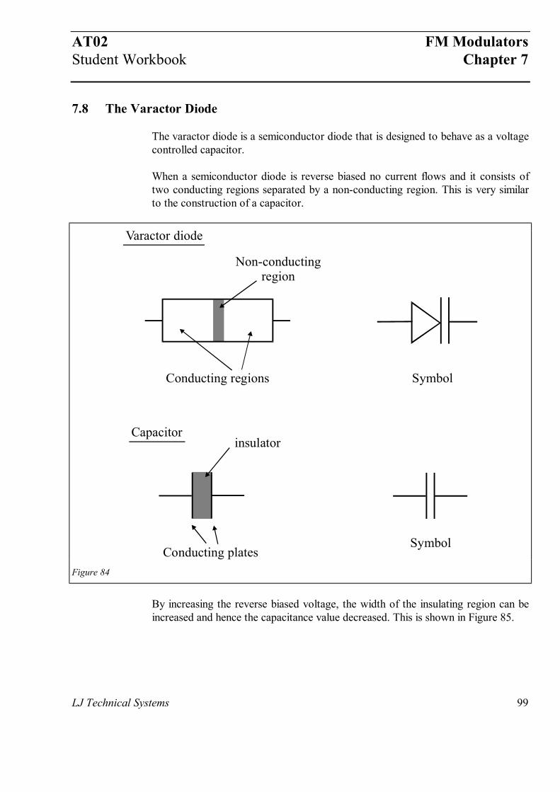
7.8 The Varactor Diode
The varactor diode is a semiconductor diode that is designed to behave as a voltagecontrolled capacitor.
When a semiconductor diode is reverse biased no current flows and it consists oftwo conducting regions separated by a non-conducting region. This is very similarto the construction of a capacitor.
Conducting regions
Conducting plates
Non-conductingregion
insulator
Symbol
Symbol
Varactor diode
Capacitor
Figure 84
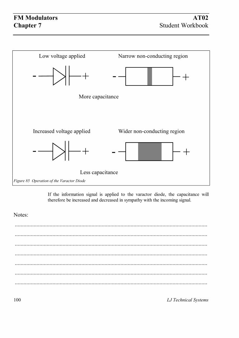
By increasing the reverse biased voltage, the width of the insulating region can beincreased and hence the capacitance value decreased. This is shown in Figure 85.
FM Modulators AT02Chapter 7 Student Workbook
100 LJ Technical Systems
- -
-
+ +
+- +
Low voltage applied Narrow non-conducting region
More capacitance
Less capacitance
Increased voltage applied Wider non-conducting region
Figure 85 Operation of the Varactor Diode
If the information signal is applied to the varactor diode, the capacitance willtherefore be increased and decreased in sympathy with the incoming signal.
Notes:
.....................................................................................................................................
.....................................................................................................................................
.....................................................................................................................................
.....................................................................................................................................
.....................................................................................................................................
.....................................................................................................................................
.....................................................................................................................................
AT02 FM ModulatorsStudent Workbook Chapter 7
LJ Technical Systems 101
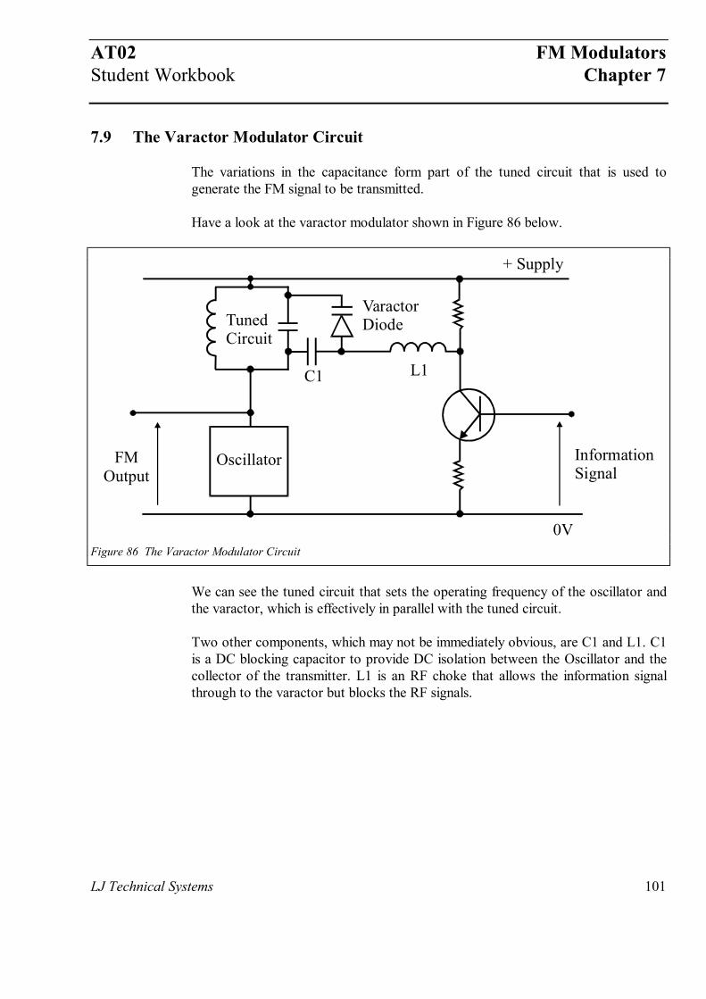
7.9 The Varactor Modulator Circuit
The variations in the capacitance form part of the tuned circuit that is used togenerate the FM signal to be transmitted.
Have a look at the varactor modulator shown in Figure 86 below.
InformationSignal
FMOutput
C1
TunedCircuit
0V
+ Supply
Oscillator
L1
VaractorDiode
Figure 86 The Varactor Modulator Circuit
We can see the tuned circuit that sets the operating frequency of the oscillator andthe varactor, which is effectively in parallel with the tuned circuit.
Two other components, which may not be immediately obvious, are C1 and L1. C1is a DC blocking capacitor to provide DC isolation between the Oscillator and thecollector of the transmitter. L1 is an RF choke that allows the information signalthrough to the varactor but blocks the RF signals.
FM Modulators AT02Chapter 7 Student Workbook
102 LJ Technical Systems
7.10 The Operation of the Varactor Modulator
(i) The information signal is applied to the base of the input transistor andappears amplified and inverted at the collector.
(ii) This low frequency signal passes through the RF choke and is applied acrossthe varactor diode.
(iii) The varactor diode changes its capacitance in sympathy with the informationsignal and therefore changes the total value of the capacitance in the tunedcircuit.
(iv) The changing value of capacitance causes the oscillator frequency to increaseand decrease under the control of the information signal.
The output is therefore an FM signal.
7.11 Using a Transistor as a Capacitor
In this section we will discover how we can persuade a transistor to behave like acapacitor.
From previous work, we remember that when a capacitor is connected in serieswith a resistor, an alternating current flowing through the circuit will be out ofphase with the voltage across the capacitor.
The current will LEAD the voltage across the capacitor by 90° and will be INPHASE with the voltage across the resistor.
To make the transistor appear to be a capacitor, all we have to do is to find a wayof making it generate a current that is leading an applied voltage. If it does this thenit is behaving like a capacitor.
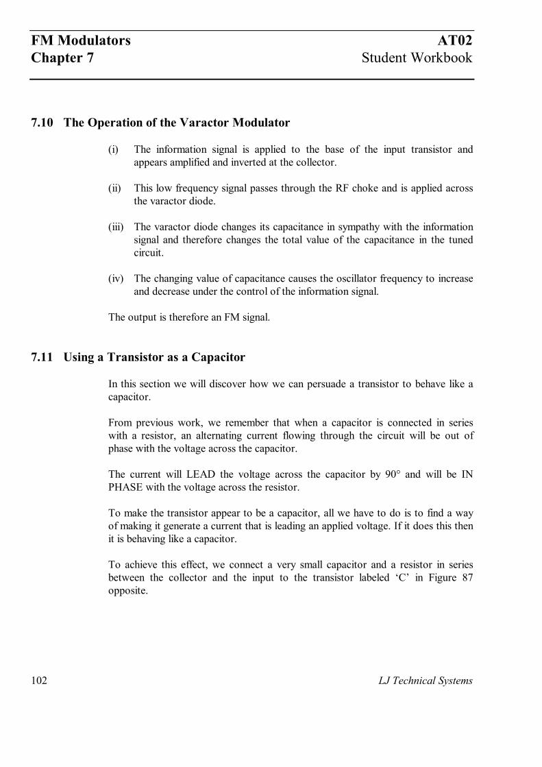
To achieve this effect, we connect a very small capacitor and a resistor in seriesbetween the collector and the input to the transistor labeled ‘C’ in Figure 87opposite.
AT02 FM ModulatorsStudent Workbook Chapter 7
LJ Technical Systems 103
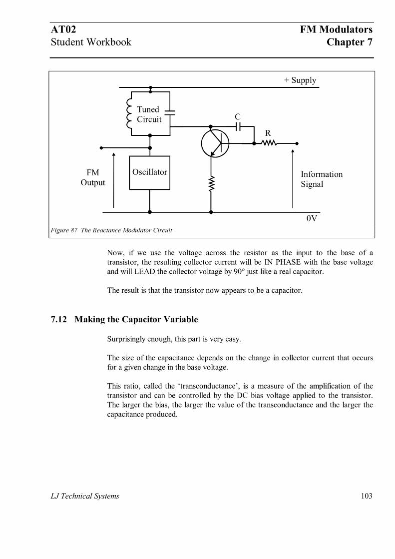
InformationSignal
FMOutput
CTunedCircuit
Oscillator
0V
+ Supply
R
Figure 87 The Reactance Modulator Circuit
Now, if we use the voltage across the resistor as the input to the base of atransistor, the resulting collector current will be IN PHASE with the base voltageand will LEAD the collector voltage by 90° just like a real capacitor.
The result is that the transistor now appears to be a capacitor.
7.12 Making the Capacitor Variable
Surprisingly enough, this part is very easy.
The size of the capacitance depends on the change in collector current that occursfor a given change in the base voltage.
This ratio, called the ‘transconductance’, is a measure of the amplification of thetransistor and can be controlled by the DC bias voltage applied to the transistor.The larger the bias, the larger the value of the transconductance and the larger thecapacitance produced.
FM Modulators AT02Chapter 7 Student Workbook
104 LJ Technical Systems
7.13 The Reactance Modulator Circuit
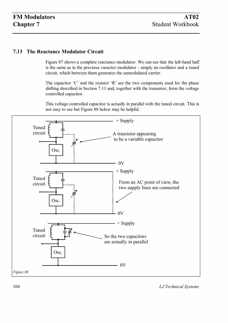
Figure 87 shows a complete reactance modulator. We can see that the left-hand halfis the same as in the previous varactor modulator - simply an oscillator and a tunedcircuit, which between them generates the unmodulated carrier.
The capacitor ‘C’ and the resistor ‘R’ are the two components used for the phaseshifting described in Section 7.11 and, together with the transistor, form the voltagecontrolled capacitor.
This voltage controlled capacitor is actually in parallel with the tuned circuit. This isnot easy to see but Figure 88 below may be helpful.
A transistor appearingto be a variable capacitor
From an AC point of view, thetwo supply lines are connected
So the two capacitorsare actually in parallel
Tunedcircuit
Tunedcircuit
Tunedcircuit
Osc.
Osc.
Osc.
0V
0V
0V
+ Supply
+ Supply
+ Supply
Figure 88
AT02 FM ModulatorsStudent Workbook Chapter 7
LJ Technical Systems 105
In the first part of the diagram, the capacitor and associated components have beenreplaced by the variable capacitor, shown dotted.
In the next part, the two supply lines are connected together. We can justify this bysaying that the output of the DC power supply always includes a large smoothingcapacitor to keep the DC voltages at a steady value. This large capacitor will have avery low reactance at the frequencies being used in the circuit - less than a milli-ohm. We can safely ignore this and so the two supply lines can be assumed to bejoined together. Remember that this does not affect the DC potentials, whichremain at the normal supply voltages.
If the two supply lines are at the same AC potential, the actual points of connectiondo not matter and so we can redraw the circuit as shown in the third part of thediagram.
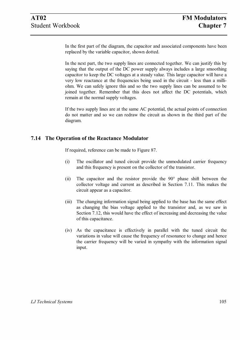
7.14 The Operation of the Reactance Modulator
If required, reference can be made to Figure 87.
(i) The oscillator and tuned circuit provide the unmodulated carrier frequencyand this frequency is present on the collector of the transistor.
(ii) The capacitor and the resistor provide the 90° phase shift between thecollector voltage and current as described in Section 7.11. This makes thecircuit appear as a capacitor.
(iii) The changing information signal being applied to the base has the same effectas changing the bias voltage applied to the transistor and, as we saw inSection 7.12, this would have the effect of increasing and decreasing the valueof this capacitance.
(iv) As the capacitance is effectively in parallel with the tuned circuit thevariations in value will cause the frequency of resonance to change and hencethe carrier frequency will be varied in sympathy with the information signalinput.
FM Modulators AT02Chapter 7 Student Workbook
106 LJ Technical Systems
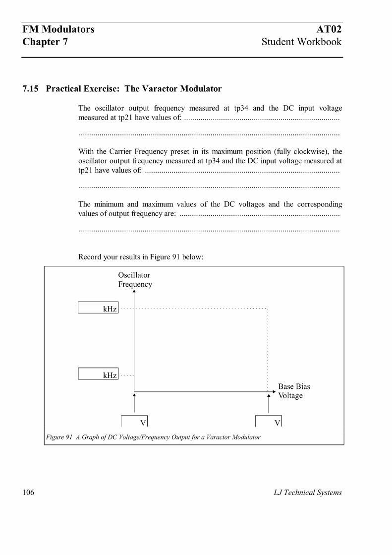
7.15 Practical Exercise: The Varactor Modulator
The oscillator output frequency measured at tp34 and the DC input voltagemeasured at tp21 have values of: ............................................................................
...............................................................................................................................
With the Carrier Frequency preset in its maximum position (fully clockwise), theoscillator output frequency measured at tp34 and the DC input voltage measured attp21 have values of: ...............................................................................................
...............................................................................................................................
The minimum and maximum values of the DC voltages and the correspondingvalues of output frequency are: ..............................................................................
...............................................................................................................................
Record your results in Figure 91 below:
OscillatorFrequency
Base BiasVoltage
kHz
kHz
V V
Figure 91 A Graph of DC Voltage/Frequency Output for a Varactor Modulator
AT02 FM ModulatorsStudent Workbook Chapter 7
LJ Technical Systems 107
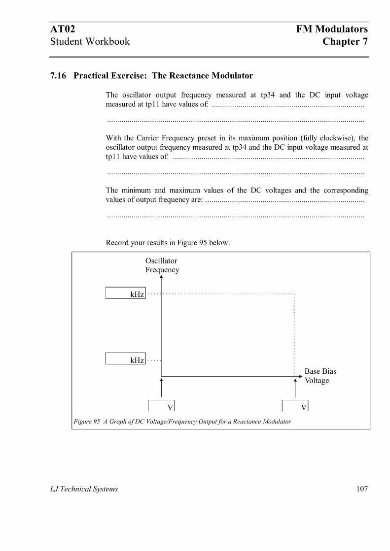
7.16 Practical Exercise: The Reactance Modulator
The oscillator output frequency measured at tp34 and the DC input voltagemeasured at tp11 have values of: ...........................................................................
..............................................................................................................................
With the Carrier Frequency preset in its maximum position (fully clockwise), theoscillator output frequency measured at tp34 and the DC input voltage measured attp11 have values of: ..............................................................................................
..............................................................................................................................
The minimum and maximum values of the DC voltages and the correspondingvalues of output frequency are: ..............................................................................
..............................................................................................................................
Record your results in Figure 95 below:
OscillatorFrequency
Base BiasVoltage
kHz
kHz
V V
Figure 95 A Graph of DC Voltage/Frequency Output for a Reactance Modulator
FM Modulators AT02Chapter 7 Student Workbook
108 LJ Technical Systems
Notes:
.....................................................................................................................................
.....................................................................................................................................
.....................................................................................................................................
.....................................................................................................................................
.....................................................................................................................................
.....................................................................................................................................
.....................................................................................................................................
.....................................................................................................................................
.....................................................................................................................................
.....................................................................................................................................
.....................................................................................................................................
.....................................................................................................................................
.....................................................................................................................................
.....................................................................................................................................
.....................................................................................................................................
.....................................................................................................................................
.....................................................................................................................................
.....................................................................................................................................
.....................................................................................................................................
.....................................................................................................................................
.....................................................................................................................................
.....................................................................................................................................
.....................................................................................................................................
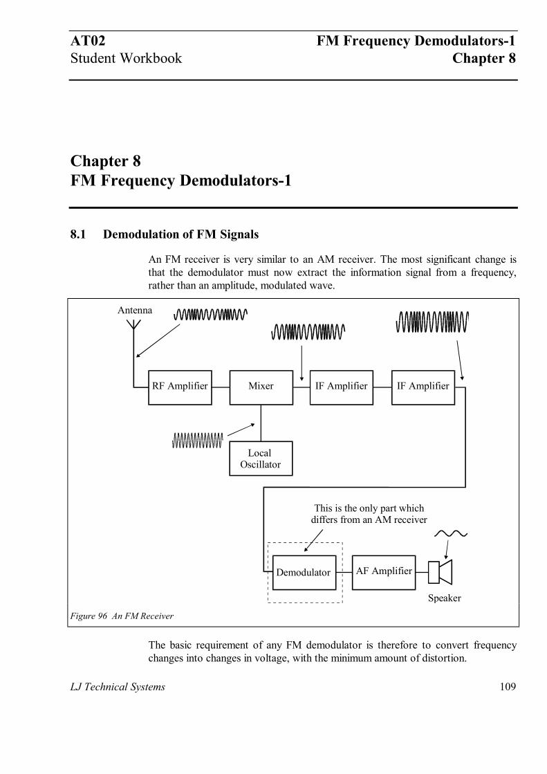
AT02 FM Frequency Demodulators-1Student Workbook Chapter 8
Chapter 8FM Frequency Demodulators-1
LJ Technical Systems 109
8.1 Demodulation of FM Signals
An FM receiver is very similar to an AM receiver. The most significant change isthat the demodulator must now extract the information signal from a frequency,rather than an amplitude, modulated wave.
Antenna
RF Amplifier Mixer IF Amplifier IF Amplifier
Demodulator AF Amplifier
Speaker
LocalOscillator
This is the only part whichdiffers from an AM receiver
Figure 96 An FM Receiver
The basic requirement of any FM demodulator is therefore to convert frequencychanges into changes in voltage, with the minimum amount of distortion.
FM Frequency Demodulators-1 AT02Chapter 8 Student Workbook
110 LJ Technical Systems
To achieve this, it should ideally have a linear voltage/frequency characteristic,similar to that shown in Figure 97 below:
Amplitude ofOutput Signal
Input Frequency
FM Signal
AM Signal
A straight characteristiccauses no distortion
Figure 97 An ‘Ideal’ Linear Voltage/Frequency Characteristic
A ‘demodulator’ can also be called a ‘discriminator’ or a ‘detector’.
Any design of circuit that has a linear voltage/frequency characteristic would beacceptable and we are going to consider the five most popular types.
In each case the main points to look for are:
• How do they convert FM signals into AM signals?
• How linear is their response - this determines the amount of distortion in the final output?
• How good are they at rejecting noise signals?
AT02 FM Frequency Demodulators-1Student Workbook Chapter 8
LJ Technical Systems 111
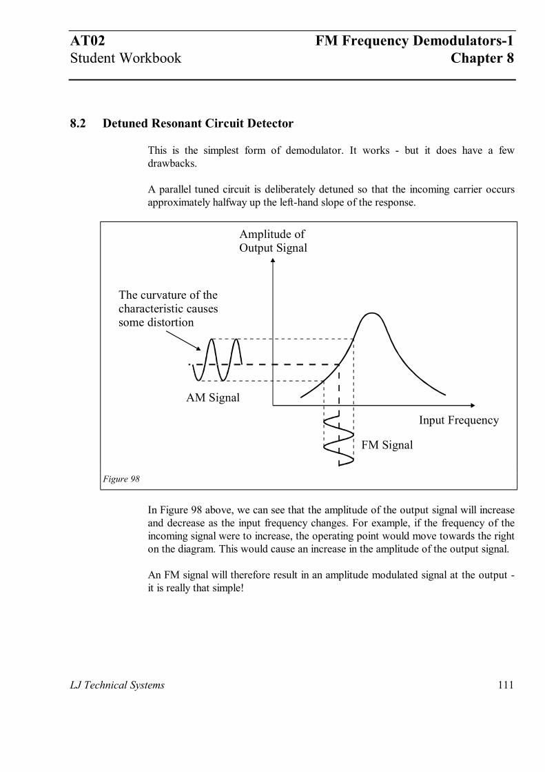
8.2 Detuned Resonant Circuit Detector
This is the simplest form of demodulator. It works - but it does have a fewdrawbacks.
A parallel tuned circuit is deliberately detuned so that the incoming carrier occursapproximately halfway up the left-hand slope of the response.
Amplitude ofOutput Signal
Input Frequency
The curvature of thecharacteristic causessome distortion
FM Signal
AM Signal
Figure 98
In Figure 98 above, we can see that the amplitude of the output signal will increaseand decrease as the input frequency changes. For example, if the frequency of theincoming signal were to increase, the operating point would move towards the righton the diagram. This would cause an increase in the amplitude of the output signal.
An FM signal will therefore result in an amplitude modulated signal at the output -it is really that simple!
FM Frequency Demodulators-1 AT02Chapter 8 Student Workbook
112 LJ Technical Systems
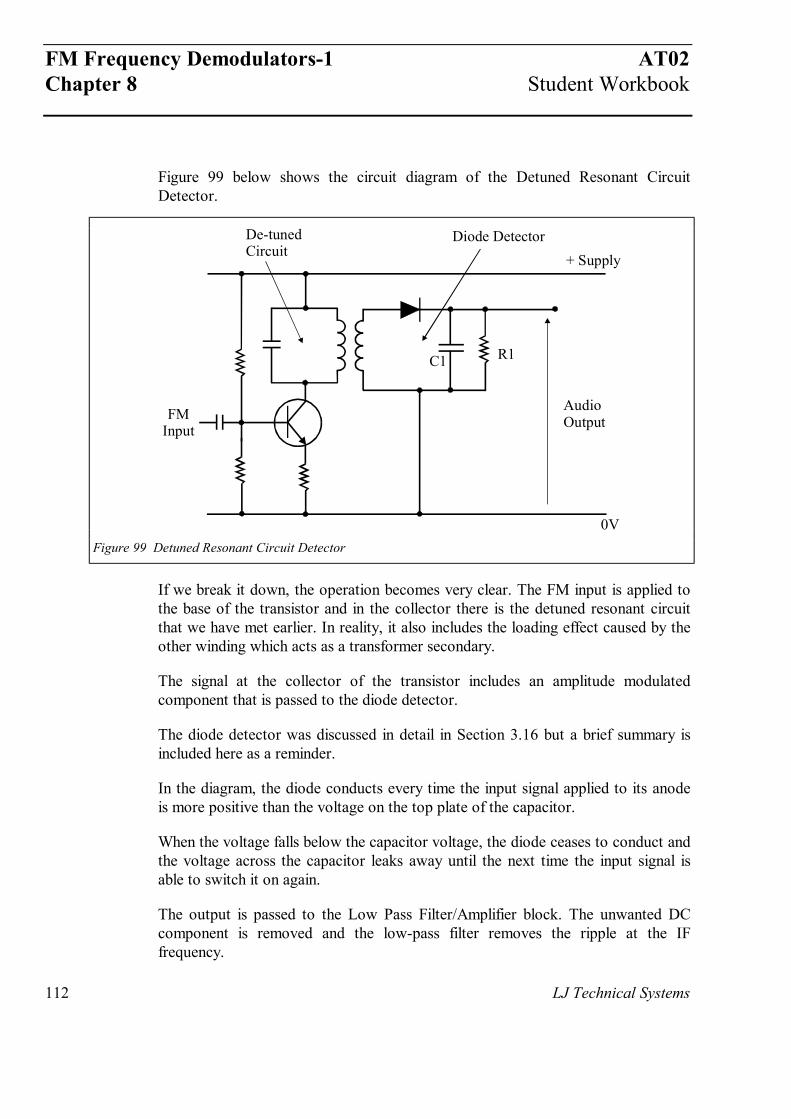
Figure 99 below shows the circuit diagram of the Detuned Resonant CircuitDetector.
AudioOutputFM
Input
C1
De-tunedCircuit
0V
+ SupplyDiode Detector
R1
Figure 99 Detuned Resonant Circuit Detector
If we break it down, the operation becomes very clear. The FM input is applied tothe base of the transistor and in the collector there is the detuned resonant circuitthat we have met earlier. In reality, it also includes the loading effect caused by theother winding which acts as a transformer secondary.
The signal at the collector of the transistor includes an amplitude modulatedcomponent that is passed to the diode detector.
The diode detector was discussed in detail in Section 3.16 but a brief summary isincluded here as a reminder.
In the diagram, the diode conducts every time the input signal applied to its anodeis more positive than the voltage on the top plate of the capacitor.
When the voltage falls below the capacitor voltage, the diode ceases to conduct andthe voltage across the capacitor leaks away until the next time the input signal isable to switch it on again.
The output is passed to the Low Pass Filter/Amplifier block. The unwanted DCcomponent is removed and the low-pass filter removes the ripple at the IFfrequency.
AT02 FM Frequency Demodulators-1Student Workbook Chapter 8
LJ Technical Systems 113
One disadvantage is that any noise spikes included in the incoming signal will alsobe passed through the diode detector and appear at the output. If we are going toavoid this problem, we must remove the AM noise before the input to thedemodulator. We do this with an Amplitude Limiter circuit.
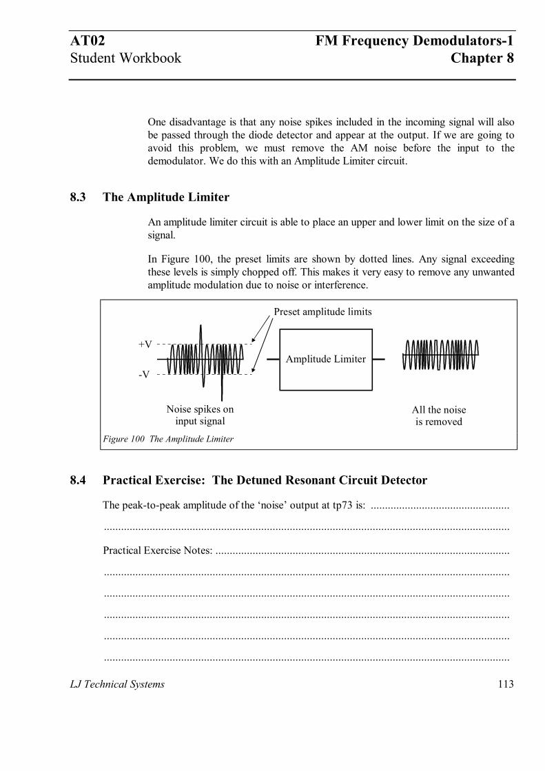
8.3 The Amplitude Limiter
An amplitude limiter circuit is able to place an upper and lower limit on the size of asignal.
In Figure 100, the preset limits are shown by dotted lines. Any signal exceedingthese levels is simply chopped off. This makes it very easy to remove any unwantedamplitude modulation due to noise or interference.
Noise spikes oninput signal
All the noiseis removed
+V
-VAmplitude Limiter
Preset amplitude limits
Figure 100 The Amplitude Limiter
8.4 Practical Exercise: The Detuned Resonant Circuit Detector
The peak-to-peak amplitude of the ‘noise’ output at tp73 is: .................................................
..............................................................................................................................................
Practical Exercise Notes: .......................................................................................................
..............................................................................................................................................
..............................................................................................................................................
..............................................................................................................................................
..............................................................................................................................................
..............................................................................................................................................
FM Frequency Demodulators-1 AT02Chapter 8 Student Workbook
114 LJ Technical Systems
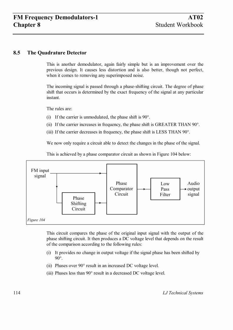
8.5 The Quadrature Detector
This is another demodulator, again fairly simple but is an improvement over theprevious design. It causes less distortion and is also better, though not perfect,when it comes to removing any superimposed noise.
The incoming signal is passed through a phase-shifting circuit. The degree of phaseshift that occurs is determined by the exact frequency of the signal at any particularinstant.
The rules are:
(i) If the carrier is unmodulated, the phase shift is 90°.(ii) If the carrier increases in frequency, the phase shift is GREATER THAN 90°.(iii) If the carrier decreases in frequency, the phase shift is LESS THAN 90°.
We now only require a circuit able to detect the changes in the phase of the signal.
This is achieved by a phase comparator circuit as shown in Figure 104 below:
PhaseShiftingCircuit
LowPassFilter
PhaseComparator
Circuit
FM inputsignal
Audiooutputsignal
Figure 104
This circuit compares the phase of the original input signal with the output of thephase shifting circuit. It then produces a DC voltage level that depends on the resultof the comparison according to the following rules:
(i) It provides no change in output voltage if the signal phase has been shifted by 90°.
(ii) Phases over 90° result in an increased DC voltage level.(iii) Phases less than 90° result in a decreased DC voltage level.
AT02 FM Frequency Demodulators-1Student Workbook Chapter 8
LJ Technical Systems 115
As the phase changes, the DC voltage level moves up and down and re-creates theaudio signal.
A low pass filter is included to reduce the amplitude of any high-frequency rippleand also blocks the DC offset. Consequently, the signal at the output closelyresembles the original input signal.
The characteristic as shown in Figure 105 is straight enough to cause very littledistortion to the final audio output.
Amplitude
Frequency
FM Input Signal
AudioOutputSignal
Figure 105 Quadrature Detector Characteristic
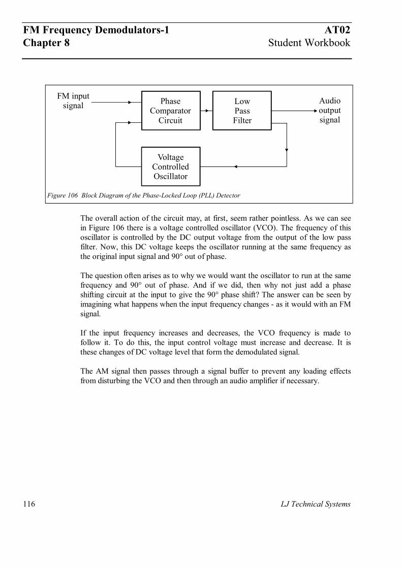
8.6 The Phase-Locked Loop (PLL) Detector
This is another demodulator that employs a phase comparator circuit. It is a verygood demodulator and has the advantage that it is available as a self-containedintegrated circuit so there is no setting up required - you plug it in and it works. Forthese reasons it is often used in commercial broadcast receivers. It has very lowlevels of distortion and is almost immune from external noise signals and providesvery low levels of distortion. Altogether a very nice circuit.
FM Frequency Demodulators-1 AT02Chapter 8 Student Workbook
116 LJ Technical Systems
VoltageControlledOscillator
LowPassFilter
PhaseComparator
Circuit
FM inputsignal Audio
outputsignal
Figure 106 Block Diagram of the Phase-Locked Loop (PLL) Detector
The overall action of the circuit may, at first, seem rather pointless. As we can seein Figure 106 there is a voltage controlled oscillator (VCO). The frequency of thisoscillator is controlled by the DC output voltage from the output of the low passfilter. Now, this DC voltage keeps the oscillator running at the same frequency asthe original input signal and 90° out of phase.
The question often arises as to why we would want the oscillator to run at the samefrequency and 90° out of phase. And if we did, then why not just add a phaseshifting circuit at the input to give the 90° phase shift? The answer can be seen byimagining what happens when the input frequency changes - as it would with an FMsignal.
If the input frequency increases and decreases, the VCO frequency is made tofollow it. To do this, the input control voltage must increase and decrease. It isthese changes of DC voltage level that form the demodulated signal.
The AM signal then passes through a signal buffer to prevent any loading effectsfrom disturbing the VCO and then through an audio amplifier if necessary.
AT02 FM Frequency Demodulators-1Student Workbook Chapter 8
LJ Technical Systems 117
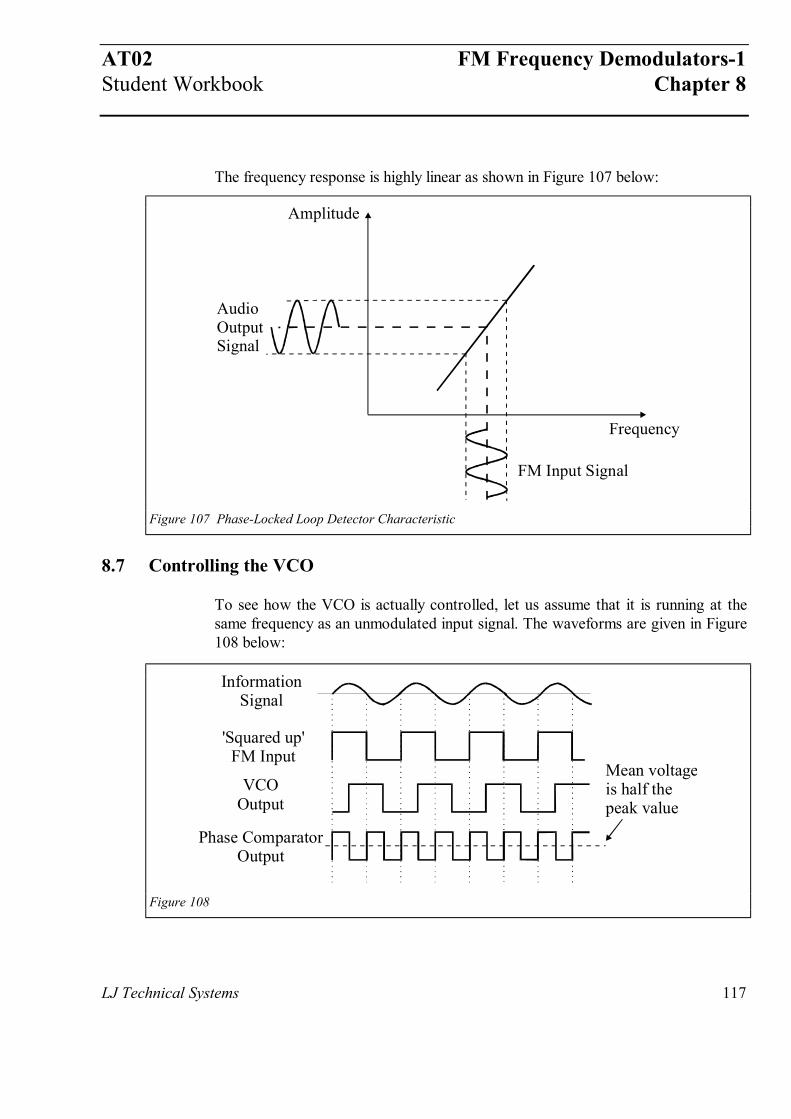
The frequency response is highly linear as shown in Figure 107 below:
Amplitude
Frequency
FM Input Signal
AudioOutputSignal
Figure 107 Phase-Locked Loop Detector Characteristic
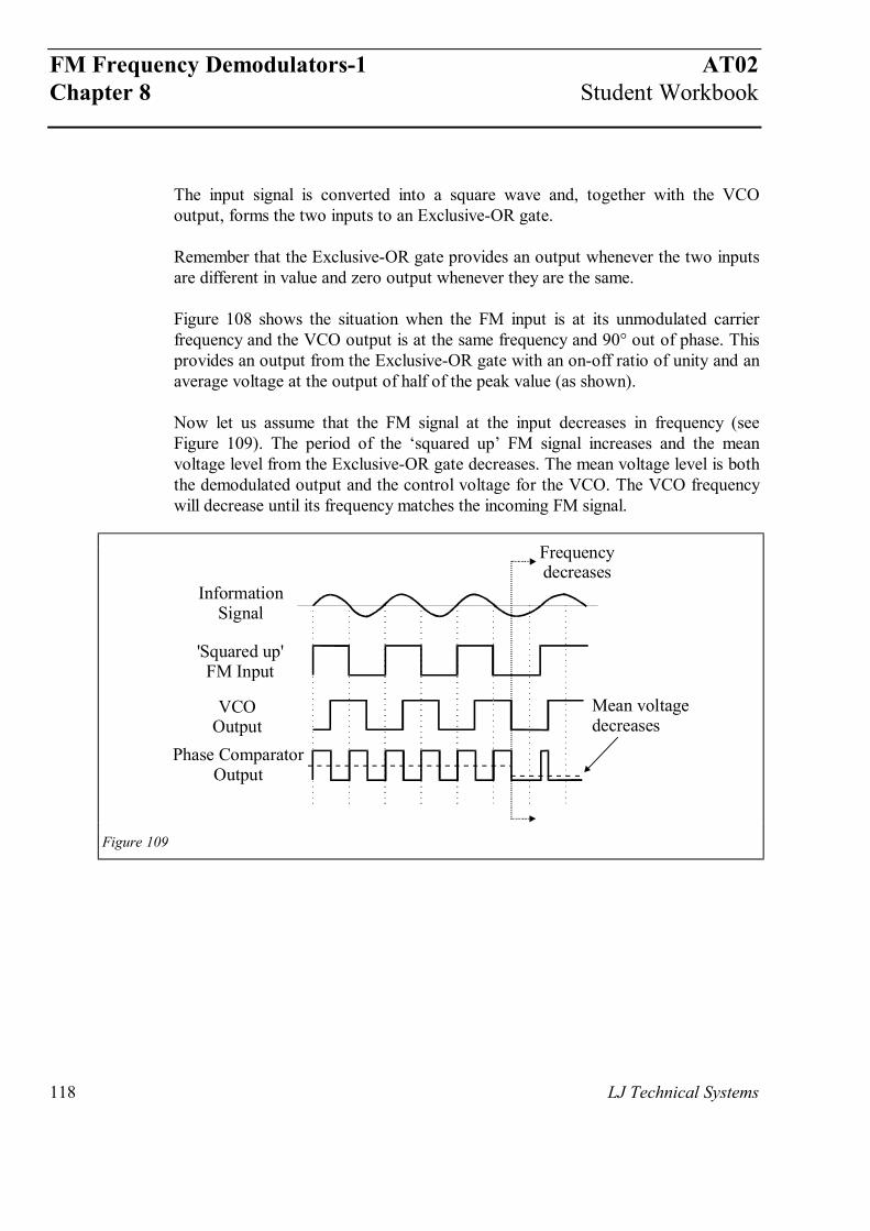
8.7 Controlling the VCO
To see how the VCO is actually controlled, let us assume that it is running at thesame frequency as an unmodulated input signal. The waveforms are given in Figure108 below:
InformationSignal
'Squared up'FM Input
VCOOutput
Phase ComparatorOutput
Mean voltageis half thepeak value
Figure 108
FM Frequency Demodulators-1 AT02Chapter 8 Student Workbook
118 LJ Technical Systems
The input signal is converted into a square wave and, together with the VCOoutput, forms the two inputs to an Exclusive-OR gate.
Remember that the Exclusive-OR gate provides an output whenever the two inputsare different in value and zero output whenever they are the same.
Figure 108 shows the situation when the FM input is at its unmodulated carrierfrequency and the VCO output is at the same frequency and 90° out of phase. Thisprovides an output from the Exclusive-OR gate with an on-off ratio of unity and anaverage voltage at the output of half of the peak value (as shown).
Now let us assume that the FM signal at the input decreases in frequency (seeFigure 109). The period of the ‘squared up’ FM signal increases and the meanvoltage level from the Exclusive-OR gate decreases. The mean voltage level is boththe demodulated output and the control voltage for the VCO. The VCO frequencywill decrease until its frequency matches the incoming FM signal.
InformationSignal
'Squared up'FM Input
VCOOutput
Phase ComparatorOutput
Frequencydecreases
Mean voltagedecreases
Figure 109
AT02 FM Frequency Demodulators-1Student Workbook Chapter 8
LJ Technical Systems 119
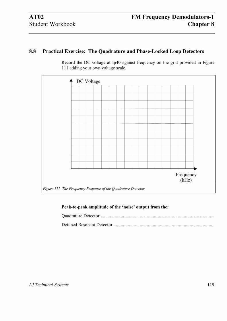
8.8 Practical Exercise: The Quadrature and Phase-Locked Loop Detectors
Record the DC voltage at tp40 against frequency on the grid provided in Figure111 adding your own voltage scale.
DC Voltage
Frequency(kHz)
Figure 111 The Frequency Response of the Quadrature Detector
Peak-to-peak amplitude of the ‘noise’ output from the:
Quadrature Detector .............................................................................................
Detuned Resonant Detector ...................................................................................
FM Frequency Demodulators-1 AT02Chapter 8 Student Workbook
120 LJ Technical Systems
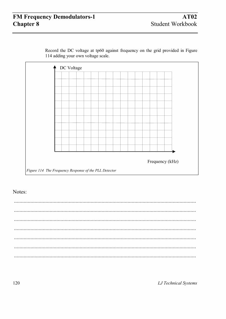
Record the DC voltage at tp60 against frequency on the grid provided in Figure114 adding your own voltage scale.
DC Voltage
Frequency (kHz)
Figure 114 The Frequency Response of the PLL Detector
Notes:
.....................................................................................................................................
.....................................................................................................................................
.....................................................................................................................................
.....................................................................................................................................
.....................................................................................................................................
.....................................................................................................................................
.....................................................................................................................................
AT02 FM Frequency Demodulators-2Student Workbook Chapter 9
Chapter 9FM Frequency Demodulators-2
LJ Technical Systems 121
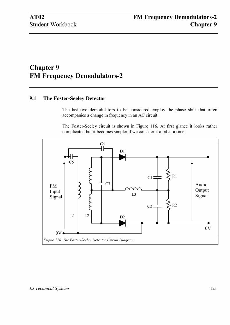
9.1 The Foster-Seeley Detector
The last two demodulators to be considered employ the phase shift that oftenaccompanies a change in frequency in an AC circuit.
The Foster-Seeley circuit is shown in Figure 116. At first glance it looks rathercomplicated but it becomes simpler if we consider it a bit at a time.
AudioOutputSignal
FMInputSignal
D1
D2
C1
C2
R1
L1 L2
C3
C4
C5
R2
L3
0V0V
Figure 116 The Foster-Seeley Detector Circuit Diagram
FM Frequency Demodulators-2 AT02Chapter 9 Student Workbook
122 LJ Technical Systems
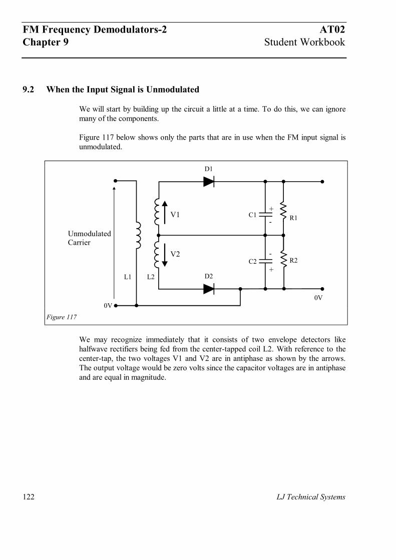
9.2 When the Input Signal is Unmodulated
We will start by building up the circuit a little at a time. To do this, we can ignoremany of the components.
Figure 117 below shows only the parts that are in use when the FM input signal isunmodulated.
UnmodulatedCarrier
D1
D2
C1
C2
R1
L1 L2
R2
0V0V
+
-
V1
V2
Figure 117
We may recognize immediately that it consists of two envelope detectors likehalfwave rectifiers being fed from the center-tapped coil L2. With reference to thecenter-tap, the two voltages V1 and V2 are in antiphase as shown by the arrows.The output voltage would be zero volts since the capacitor voltages are in antiphaseand are equal in magnitude.
AT02 FM Frequency Demodulators-2Student Workbook Chapter 9
LJ Technical Systems 123
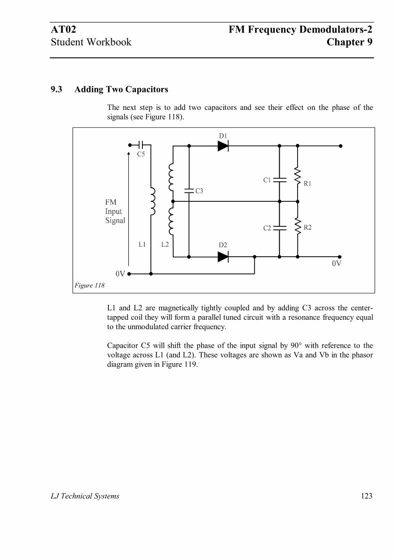
9.3 Adding Two Capacitors
The next step is to add two capacitors and see their effect on the phase of thesignals (see Figure 118).
Figure 118
L1 and L2 are magnetically tightly coupled and by adding C3 across the center-tapped coil they will form a parallel tuned circuit with a resonance frequency equalto the unmodulated carrier frequency.
Capacitor C5 will shift the phase of the input signal by 90° with reference to thevoltage across L1 (and L2). These voltages are shown as Va and Vb in the phasordiagram given in Figure 119.
FM Frequency Demodulators-2 AT02Chapter 9 Student Workbook
124 LJ Technical Systems
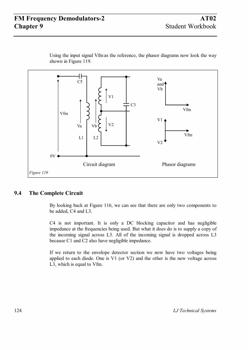
Using the input signal Vfm as the reference, the phasor diagrams now look the wayshown in Figure 119.
L1 L2
C3
C5
0V
Vfm
V1
V2Va Vb
VaandVb
Vfm
Vfm
V1
V2
Circuit diagram Phasor diagramsFigure 119
9.4 The Complete Circuit
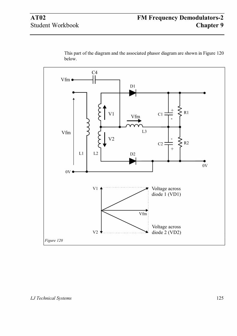
By looking back at Figure 116, we can see that there are only two components tobe added, C4 and L3.
C4 is not important. It is only a DC blocking capacitor and has negligibleimpedance at the frequencies being used. But what it does do is to supply a copy ofthe incoming signal across L3. All of the incoming signal is dropped across L3because C1 and C2 also have negligible impedance.
If we return to the envelope detector section we now have two voltages beingapplied to each diode. One is V1 (or V2) and the other is the new voltage acrossL3, which is equal to Vfm.
AT02 FM Frequency Demodulators-2Student Workbook Chapter 9
LJ Technical Systems 125
This part of the diagram and the associated phasor diagram are shown in Figure 120below.
D1
D2
C1
C2
R1
L1 L2
R2
L3
0V0V
+
-
V1
V2
Vfm
Vfm
Vfm
V1
V2
Voltage acrossdiode 1 (VD1)
Voltage acrossdiode 2 (VD2)
VfmC4
Figure 120
FM Frequency Demodulators-2 AT02Chapter 9 Student Workbook
126 LJ Technical Systems
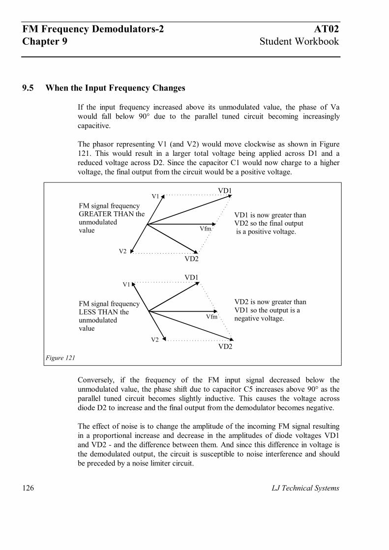
9.5 When the Input Frequency Changes
If the input frequency increased above its unmodulated value, the phase of Vawould fall below 90° due to the parallel tuned circuit becoming increasinglycapacitive.
The phasor representing V1 (and V2) would move clockwise as shown in Figure121. This would result in a larger total voltage being applied across D1 and areduced voltage across D2. Since the capacitor C1 would now charge to a highervoltage, the final output from the circuit would be a positive voltage.
Vfm
Vfm
V1
V1
V2
V2
VD1 is now greater thanVD2 so the final outputis a positive voltage.
VD2 is now greater thanVD1 so the output is anegative voltage.
VD1
VD1
VD2
VD2
FM signal frequencyLESS THAN theunmodulatedvalue
FM signal frequencyGREATER THAN theunmodulatedvalue
Figure 121
Conversely, if the frequency of the FM input signal decreased below theunmodulated value, the phase shift due to capacitor C5 increases above 90° as theparallel tuned circuit becomes slightly inductive. This causes the voltage acrossdiode D2 to increase and the final output from the demodulator becomes negative.
The effect of noise is to change the amplitude of the incoming FM signal resultingin a proportional increase and decrease in the amplitudes of diode voltages VD1and VD2 - and the difference between them. And since this difference in voltage isthe demodulated output, the circuit is susceptible to noise interference and shouldbe preceded by a noise limiter circuit.
AT02 FM Frequency Demodulators-2Student Workbook Chapter 9
LJ Technical Systems 127
9.6 The Ratio Detector
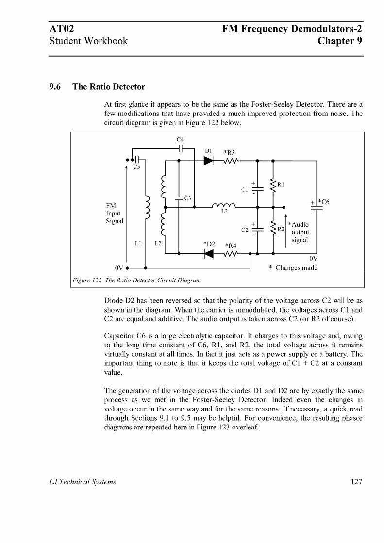
At first glance it appears to be the same as the Foster-Seeley Detector. There are afew modifications that have provided a much improved protection from noise. Thecircuit diagram is given in Figure 122 below.
Audiooutputsignal
FMInputSignal
D1
C1
C2
R1
L1 L2
C3
C4
C5
R2
L3
0V0V
*
*R3
*C6
*R4*D2
* Changes made
+
+
+-
-
-
Figure 122 The Ratio Detector Circuit Diagram
Diode D2 has been reversed so that the polarity of the voltage across C2 will be asshown in the diagram. When the carrier is unmodulated, the voltages across C1 andC2 are equal and additive. The audio output is taken across C2 (or R2 of course).
Capacitor C6 is a large electrolytic capacitor. It charges to this voltage and, owingto the long time constant of C6, R1, and R2, the total voltage across it remainsvirtually constant at all times. In fact it just acts as a power supply or a battery. Theimportant thing to note is that it keeps the total voltage of C1 + C2 at a constantvalue.
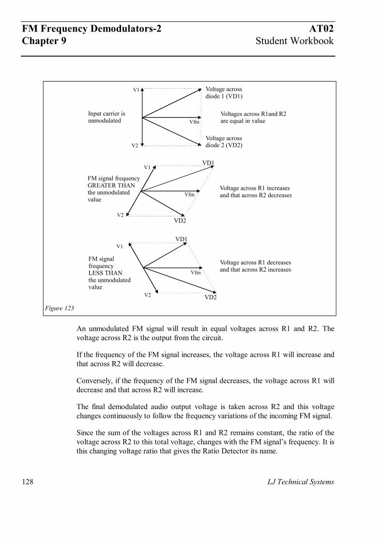
The generation of the voltage across the diodes D1 and D2 are by exactly the sameprocess as we met in the Foster-Seeley Detector. Indeed even the changes involtage occur in the same way and for the same reasons. If necessary, a quick readthrough Sections 9.1 to 9.5 may be helpful. For convenience, the resulting phasordiagrams are repeated here in Figure 123 overleaf.
FM Frequency Demodulators-2 AT02Chapter 9 Student Workbook
128 LJ Technical Systems
Vfm
Vfm
V1
V1
V2
V2
Voltage across R1 increasesand that across R2 decreases
Voltage across R1 decreasesand that across R2 increases
Voltages across R1and R2are equal in value
VD1
VD1
VD2
VD2
FM signalfrequencyLESS THANthe unmodulatedvalue
FM signal frequencyGREATER THANthe unmodulatedvalue
Vfm
V1
V2
Voltage acrossdiode 1 (VD1)
Voltage acrossdiode 2 (VD2)
Input carrier isunmodulated
Figure 123
An unmodulated FM signal will result in equal voltages across R1 and R2. Thevoltage across R2 is the output from the circuit.
If the frequency of the FM signal increases, the voltage across R1 will increase andthat across R2 will decrease.
Conversely, if the frequency of the FM signal decreases, the voltage across R1 willdecrease and that across R2 will increase.
The final demodulated audio output voltage is taken across R2 and this voltagechanges continuously to follow the frequency variations of the incoming FM signal.
Since the sum of the voltages across R1 and R2 remains constant, the ratio of thevoltage across R2 to this total voltage, changes with the FM signal’s frequency. It isthis changing voltage ratio that gives the Ratio Detector its name.
AT02 FM Frequency Demodulators-2Student Workbook Chapter 9
LJ Technical Systems 129
9.7 Reducing the Effect of Electrical Noise
This is the real purpose of C6.
If the amplitude of the FM input signal suddenly increases, the voltages VD1 andVD2 will try to increase and these in turn will try to increase the voltages acrossboth R1 and R2. However, since C6 is large, the overall voltage across R1 and R2will not respond to the fast change in input amplitude. The result is that thedemodulated audio output is unaffected by fast changes in the amplitude of theincoming FM signal.
R3 and R4 are current limiting resistors to prevent momentary high levels of currentthrough the diodes, which would cause a brief fluctuation in the output voltage.
9.8 Practical Exercise: The Foster-Seeley and Ratio Detectors
Record the DC voltage at tp52 against frequency on the grid provided in Figure125 adding your own voltage scale.
DC Voltage
440 480430 470460450 kHzFigure 125 The Frequency Response of the Foster-Seeley Detector
FM Frequency Demodulators-2 AT02Chapter 9 Student Workbook
130 LJ Technical Systems
Peak-to-peak amplitude of the ‘noise’ output from the:
Foster-Seeley Detector ..........................................................................................
Detuned Resonant Circuit Detector ........................................................................
Quadrature Detector ..............................................................................................
Record the DC voltage at tp53 against frequency on the grid provided in Figure129 adding your own voltage scale.
DC Voltage
440 480430 470460450 kHzFigure 129 The Frequency Response of the Ratio Detector
Peak-to-peak amplitude of the ‘noise’ output from the:
Ratio Detector .......................................................................................................
Foster-Seeley Detector ..........................................................................................
Detuned Resonant Circuit Detector ........................................................................
Quadrature Detector ..............................................................................................