Embed Size (px)
Citation preview
ATLCE - B4 07/03/2016
© 2016 DDC 1
07/03/2016 - 1 ATLCE - B4 - © 2016 DDC
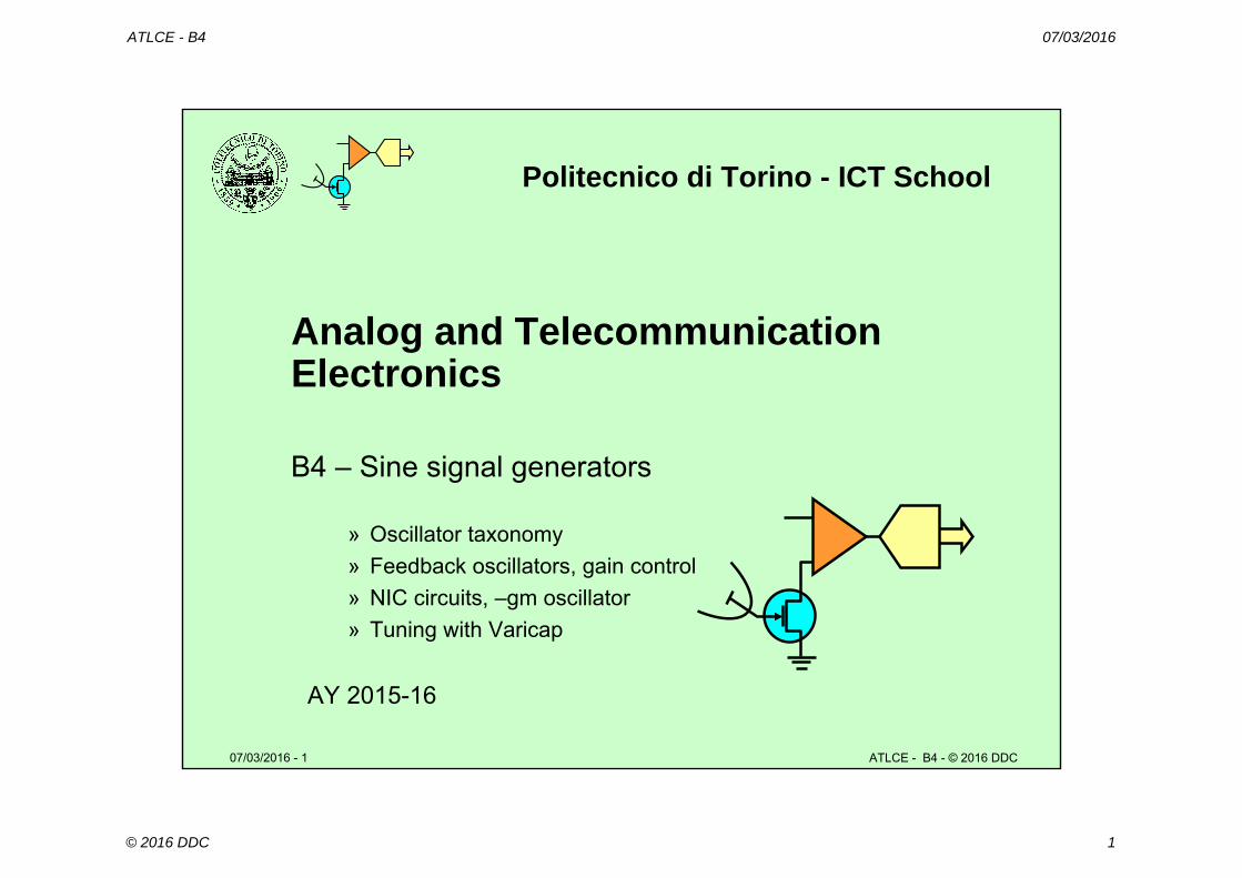
Politecnico di Torino - ICT School
Analog and Telecommunication Electronics
B4 – Sine signal generators
» Oscillator taxonomy» Feedback oscillators, gain control» NIC circuits, –gm oscillator» Tuning with Varicap
AY 2015-16
ATLCE - B4 07/03/2016
© 2016 DDC 2
07/03/2016 - 2 ATLCE - B4 - © 2016 DDC
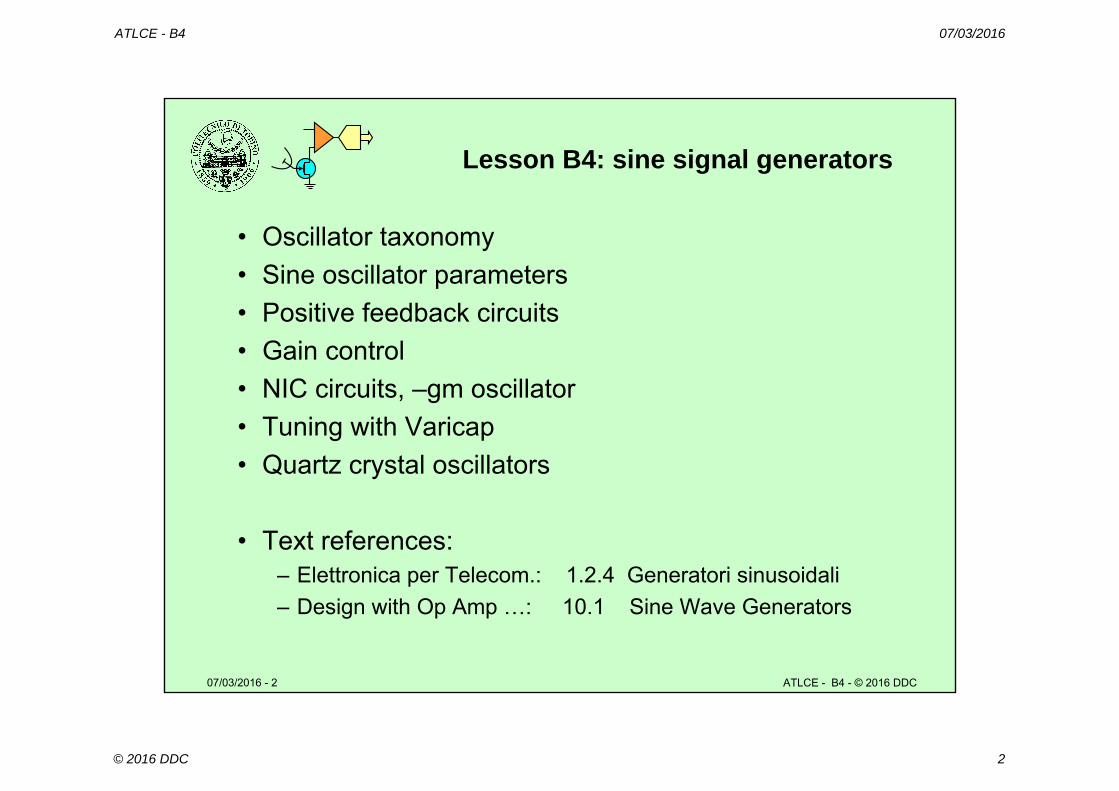
Lesson B4: sine signal generators
• Oscillator taxonomy• Sine oscillator parameters• Positive feedback circuits• Gain control• NIC circuits, –gm oscillator• Tuning with Varicap• Quartz crystal oscillators
• Text references: – Elettronica per Telecom.: 1.2.4 Generatori sinusoidali– Design with Op Amp …: 10.1 Sine Wave Generators
ATLCE - B4 07/03/2016
© 2016 DDC 3
07/03/2016 - 3 ATLCE - B4 - © 2016 DDC
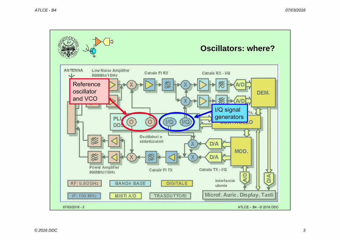
Oscillators: where?
Referenceoscillatorand VCO
I/Q signalgenerators
ATLCE - B4 07/03/2016
© 2016 DDC 4
07/03/2016 - 4 ATLCE - B4 - © 2016 DDC
Sine signal parameters
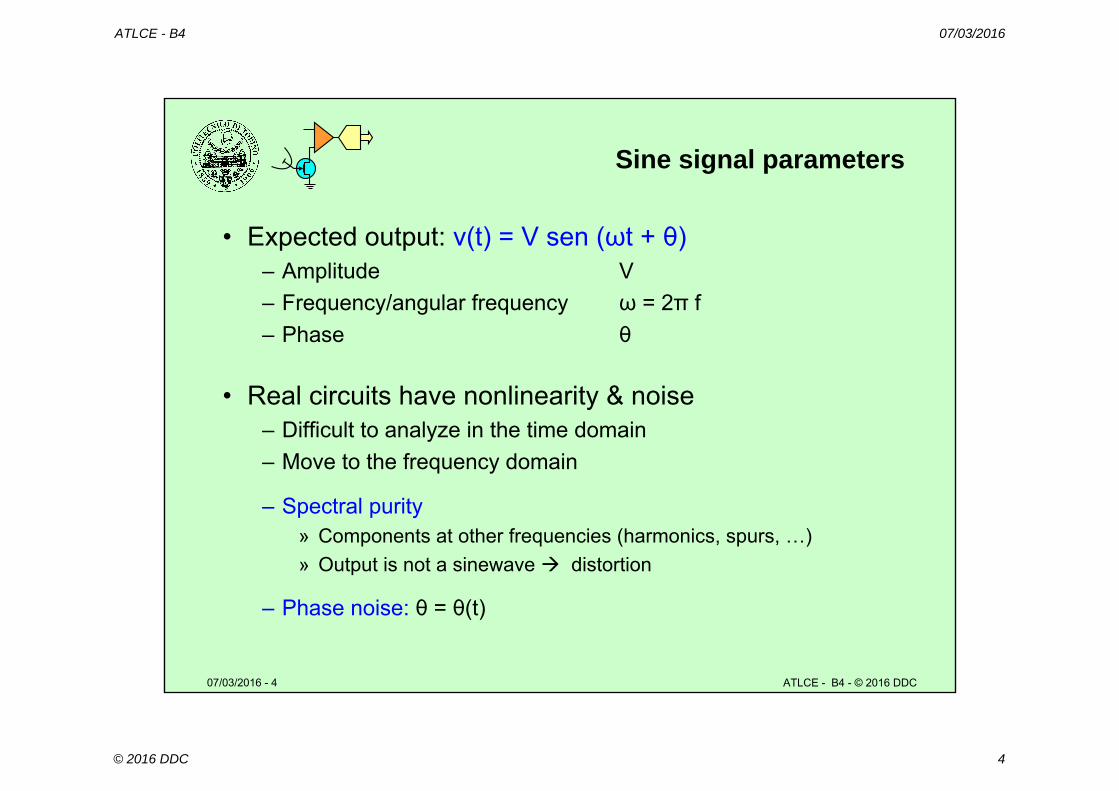
• Expected output: v(t) = V sen (ωt + θ)– Amplitude V– Frequency/angular frequency ω = 2π f– Phase θ
• Real circuits have nonlinearity & noise– Difficult to analyze in the time domain– Move to the frequency domain
– Spectral purity» Components at other frequencies (harmonics, spurs, …) » Output is not a sinewave distortion
– Phase noise: θ = θ(t)
ATLCE - B4 07/03/2016
© 2016 DDC 5
07/03/2016 - 5 ATLCE - B4 - © 2016 DDC
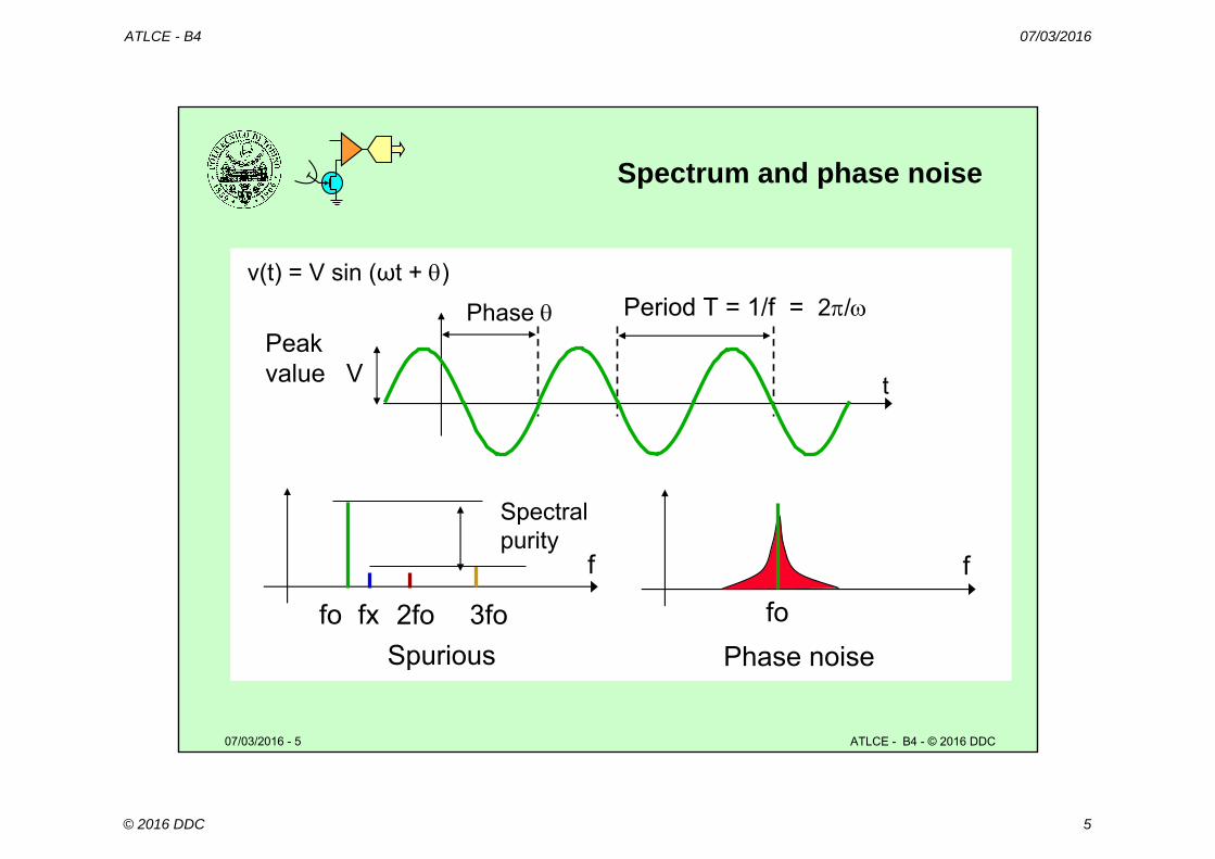
Spectrum and phase noise
fo 2fo 3fo
f
fo
v(t) = V sin (ωt + )
t
Peakvalue V
Period T = 1/f = 2/Phase
f
fxSpurious Phase noise
Spectralpurity
ATLCE - B4 07/03/2016
© 2016 DDC 6
07/03/2016 - 6 ATLCE - B4 - © 2016 DDC
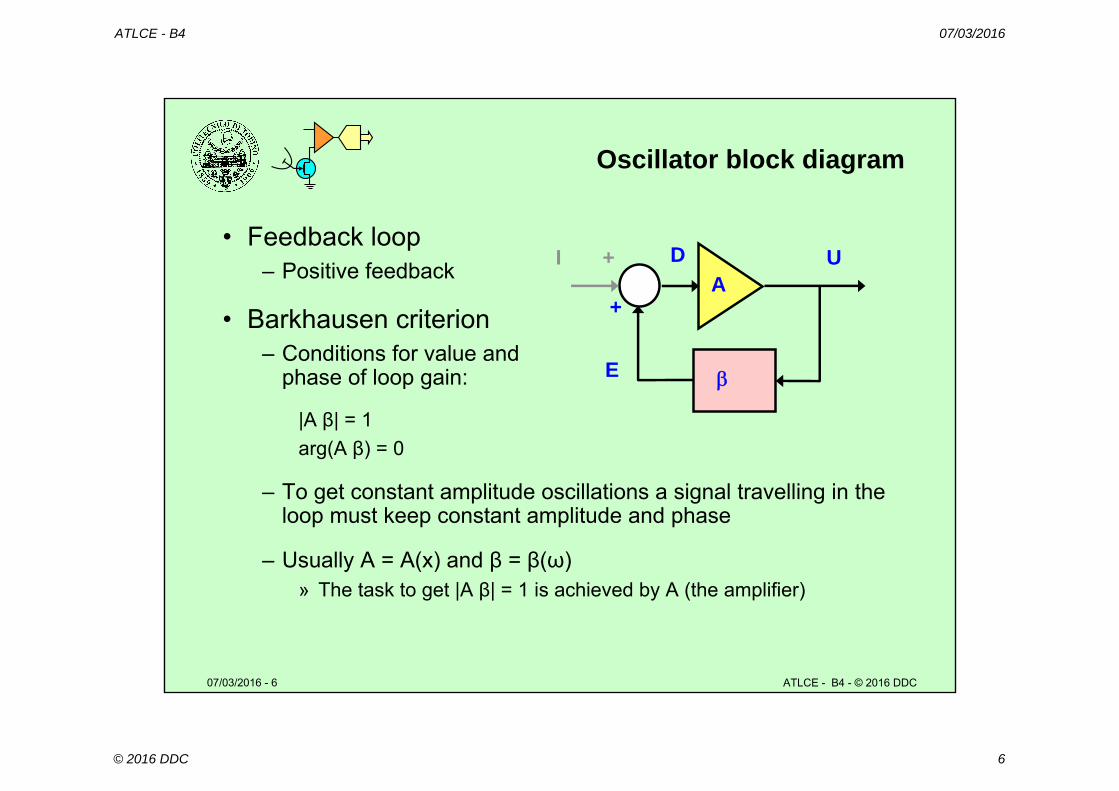
Oscillator block diagram
• Feedback loop– Positive feedback
• Barkhausen criterion– Conditions for value and
phase of loop gain:
|A β| = 1arg(A β) = 0
– To get constant amplitude oscillations a signal travelling in the loop must keep constant amplitude and phase
– Usually A = A(x) and β = β(ω)» The task to get |A β| = 1 is achieved by A (the amplifier)
I
E
A
U+ D
+
ATLCE - B4 07/03/2016
© 2016 DDC 7
07/03/2016 - 7 ATLCE - B4 - © 2016 DDC
Loop gain condition
• Goal: |A β| = 1– In most circuits A = A(x); β = β(ω)
• Condition achieved through a gain control on A– Amplifier with gain compression (nonlinearity)
• Oscillation startup– At startup the loop gain |A β| must be > 1
• Amplitude stabilization– Gain decreases as signal amplitude increases– For high signal levels |A β| < 1
• The |A| = 1 condition is met only for a specific signal level
ATLCE - B4 07/03/2016
© 2016 DDC 8
07/03/2016 - 8 ATLCE - B4 - © 2016 DDC
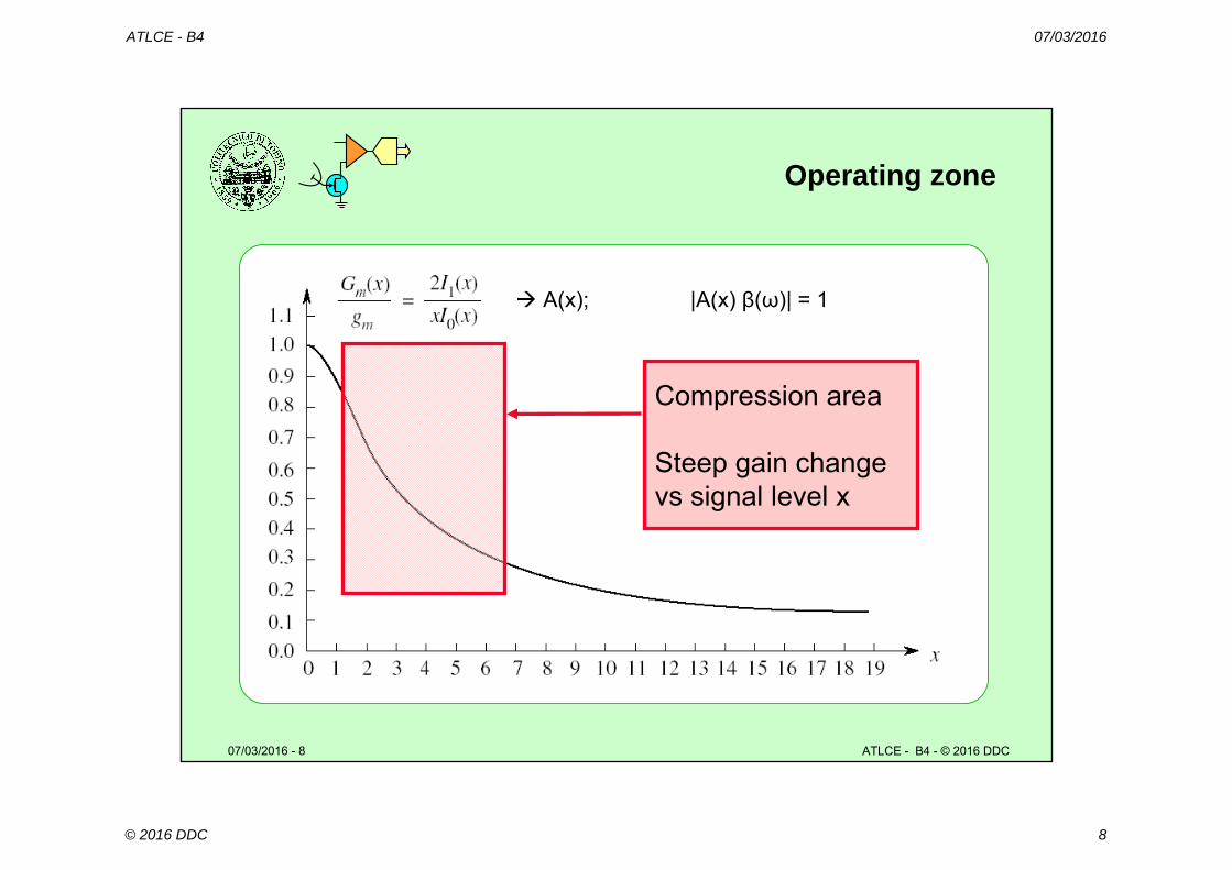
Operating zone
Compression area
Steep gain changevs signal level x
A(x); |A(x) β(ω)| = 1
ATLCE - B4 07/03/2016
© 2016 DDC 9
07/03/2016 - 9 ATLCE - B4 - © 2016 DDC
Phase control
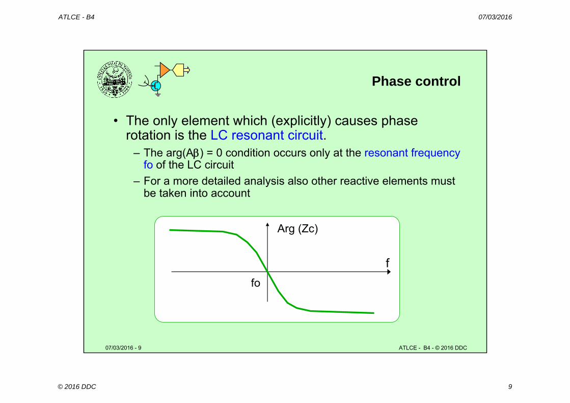
• The only element which (explicitly) causes phase rotation is the LC resonant circuit.
– The arg(A) = 0 condition occurs only at the resonant frequency fo of the LC circuit
– For a more detailed analysis also other reactive elements must be taken into account
ffo
Arg (Zc)
ATLCE - B4 07/03/2016
© 2016 DDC 10
07/03/2016 - 10 ATLCE - B4 - © 2016 DDC
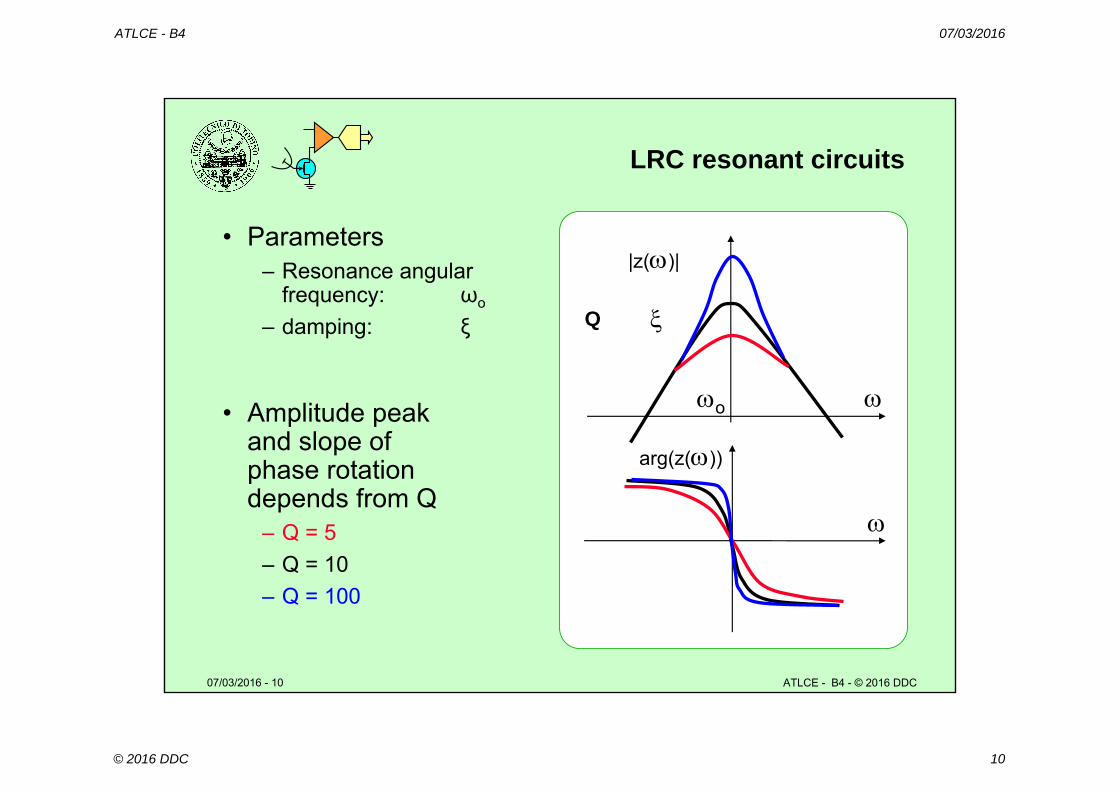
LRC resonant circuits
• Parameters– Resonance angular
frequency: ωo
– damping: ξ
• Amplitude peakand slope of phase rotation depends from Q
– Q = 5– Q = 10– Q = 100
|z()|
o
arg(z())
Q
ATLCE - B4 07/03/2016
© 2016 DDC 11
07/03/2016 - 11 ATLCE - B4 - © 2016 DDC
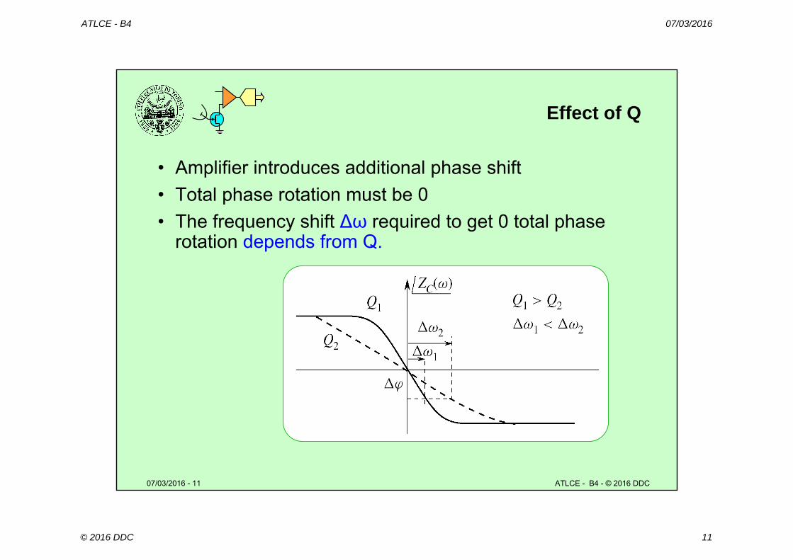
Effect of Q
• Amplifier introduces additional phase shift• Total phase rotation must be 0• The frequency shift Δω required to get 0 total phase
rotation depends from Q.
ATLCE - B4 07/03/2016
© 2016 DDC 12
07/03/2016 - 12 ATLCE - B4 - © 2016 DDC
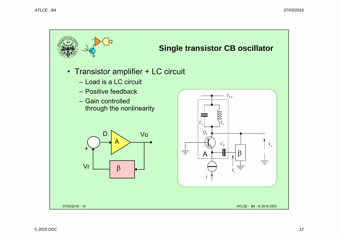
Single transistor CB oscillator
• Transistor amplifier + LC circuit– Load is a LC circuit– Positive feedback– Gain controlled
through the nonlinearity
Vr
A
VoD
+A
ATLCE - B4 07/03/2016
© 2016 DDC 13
07/03/2016 - 13 ATLCE - B4 - © 2016 DDC
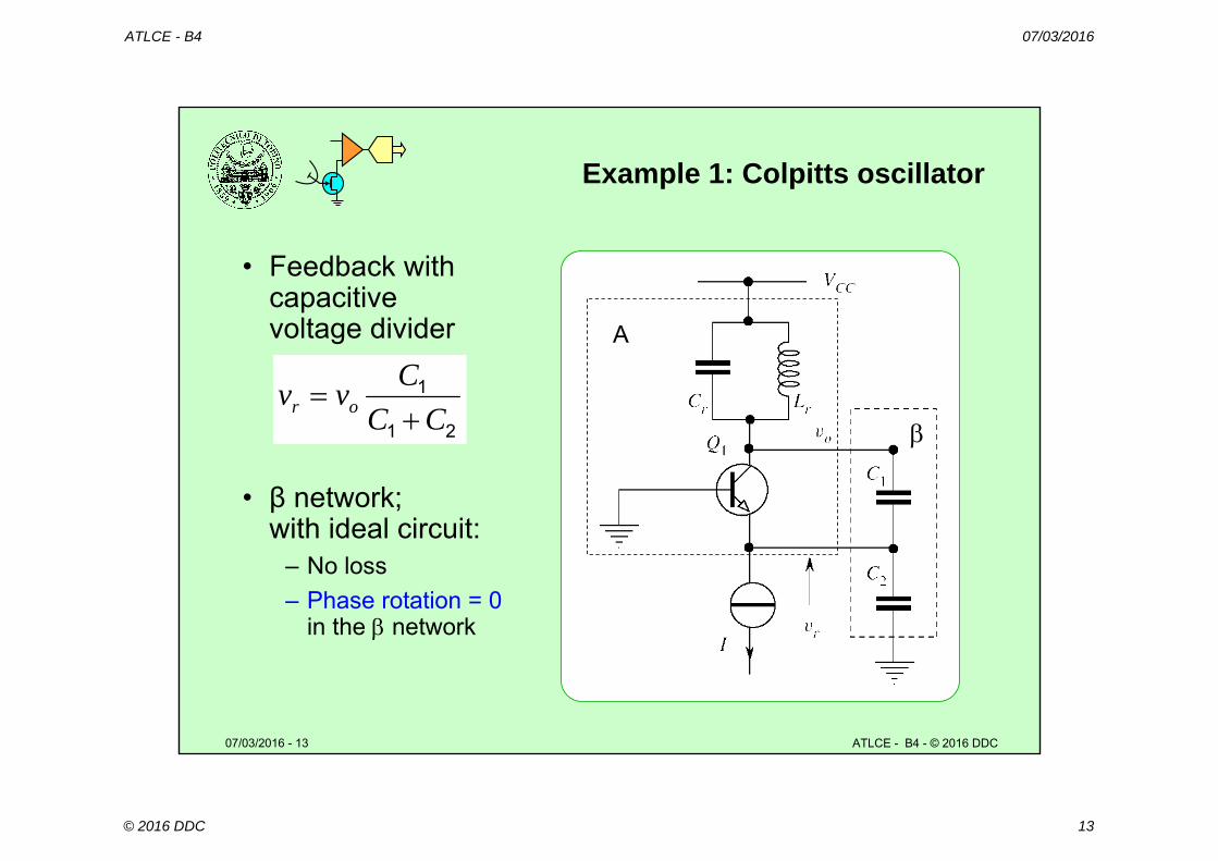
Example 1: Colpitts oscillator
• Feedback with capacitive voltage divider
• β network;with ideal circuit:
– No loss– Phase rotation = 0
in the network
A
21
1
CCCvv or
ATLCE - B4 07/03/2016
© 2016 DDC 14
07/03/2016 - 14 ATLCE - B4 - © 2016 DDC
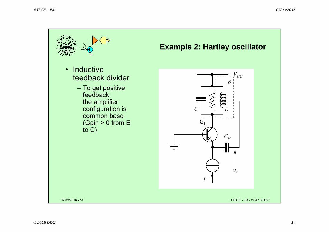
Example 2: Hartley oscillator
• Inductive feedback divider
– To get positivefeedback the amplifier configuration is common base (Gain > 0 from E to C)
ATLCE - B4 07/03/2016
© 2016 DDC 15
07/03/2016 - 15 ATLCE - B4 - © 2016 DDC
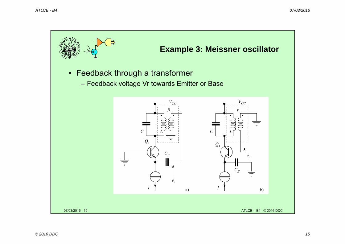
Example 3: Meissner oscillator
• Feedback through a transformer– Feedback voltage Vr towards Emitter or Base
ATLCE - B4 07/03/2016
© 2016 DDC 16
07/03/2016 - 16 ATLCE - B4 - © 2016 DDC
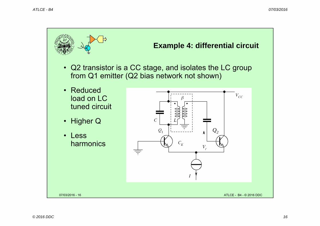
Example 4: differential circuit
• Q2 transistor is a CC stage, and isolates the LC group from Q1 emitter (Q2 bias network not shown)
• Reduced load on LC tuned circuit
• Higher Q
• Less harmonics
Q2
ATLCE - B4 07/03/2016
© 2016 DDC 17
07/03/2016 - 17 ATLCE - B4 - © 2016 DDC
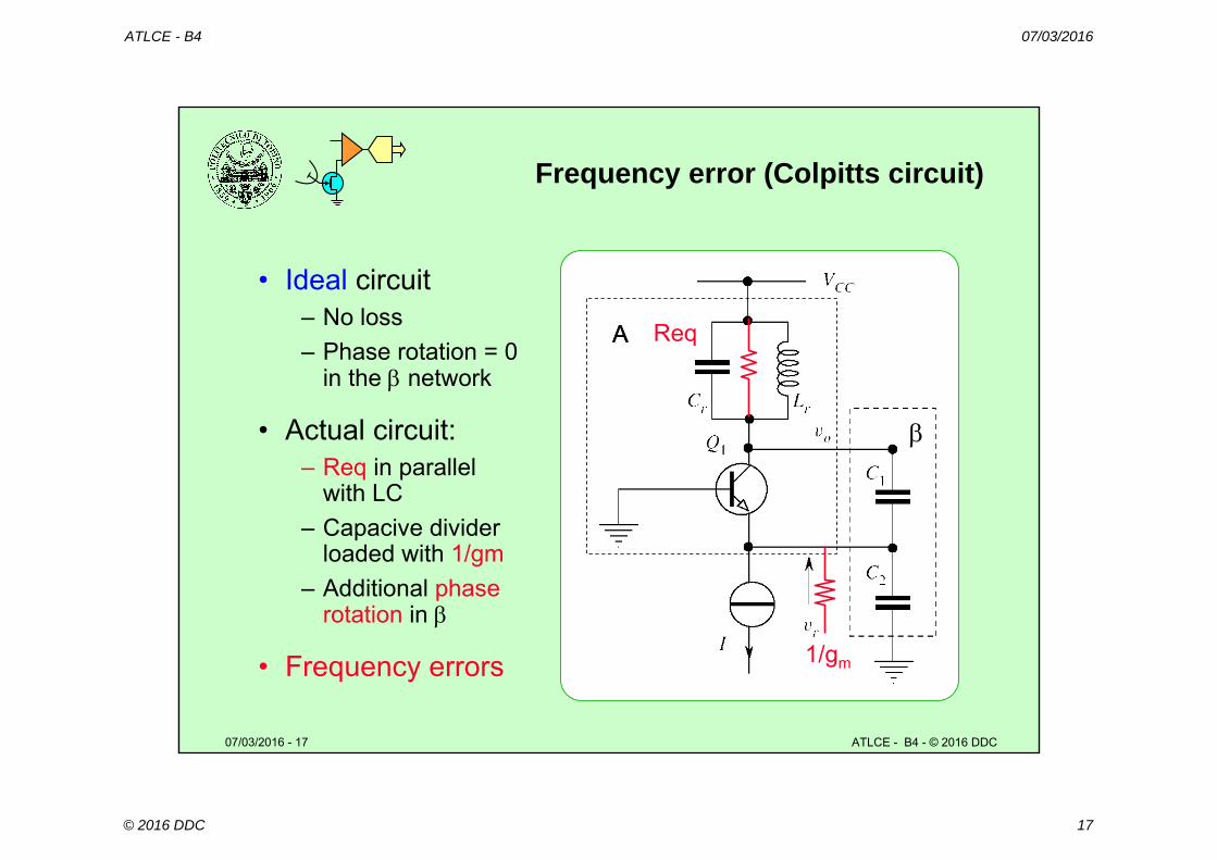
Frequency error (Colpitts circuit)
A
• Ideal circuit– No loss– Phase rotation = 0
in the network
• Actual circuit:– Req in parallel
with LC– Capacive divider
loaded with 1/gm– Additional phase
rotation in
• Frequency errors
A Req
1/gm
ATLCE - B4 07/03/2016
© 2016 DDC 18
07/03/2016 - 18 ATLCE - B4 - © 2016 DDC
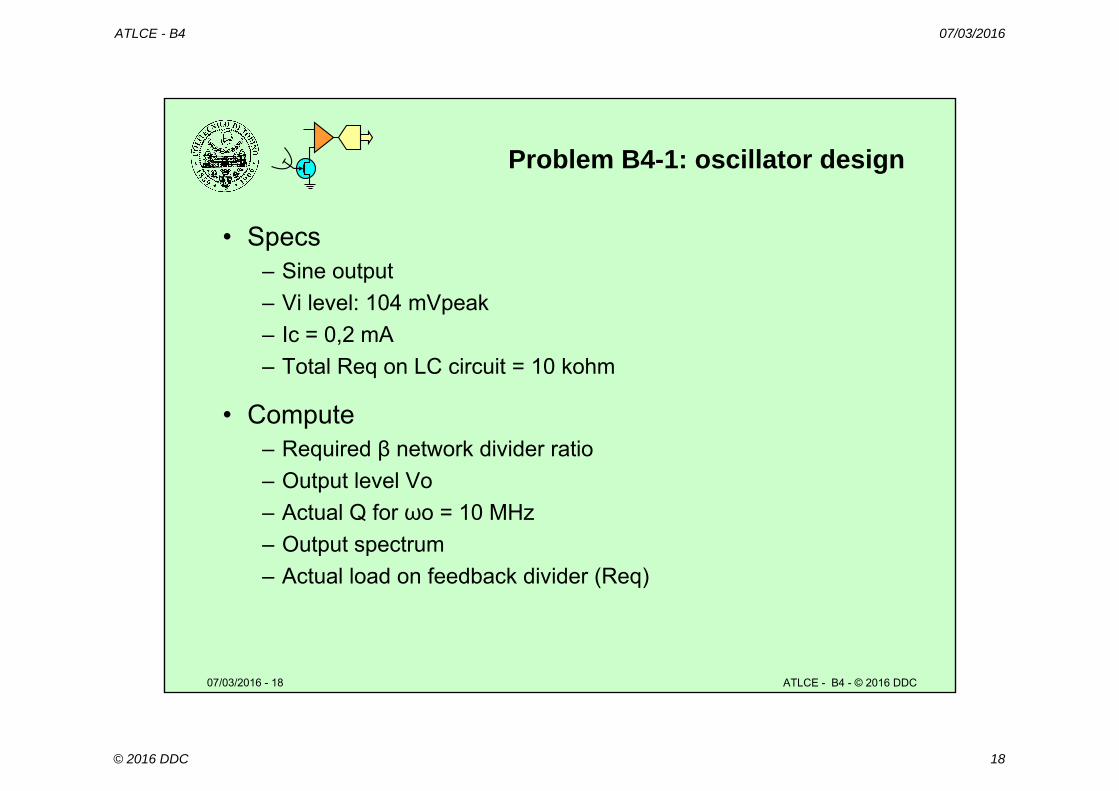
Problem B4-1: oscillator design
• Specs– Sine output– Vi level: 104 mVpeak– Ic = 0,2 mA– Total Req on LC circuit = 10 kohm
• Compute– Required β network divider ratio– Output level Vo– Actual Q for ωo = 10 MHz– Output spectrum – Actual load on feedback divider (Req)
ATLCE - B4 07/03/2016
© 2016 DDC 19
07/03/2016 - 19 ATLCE - B4 - © 2016 DDC
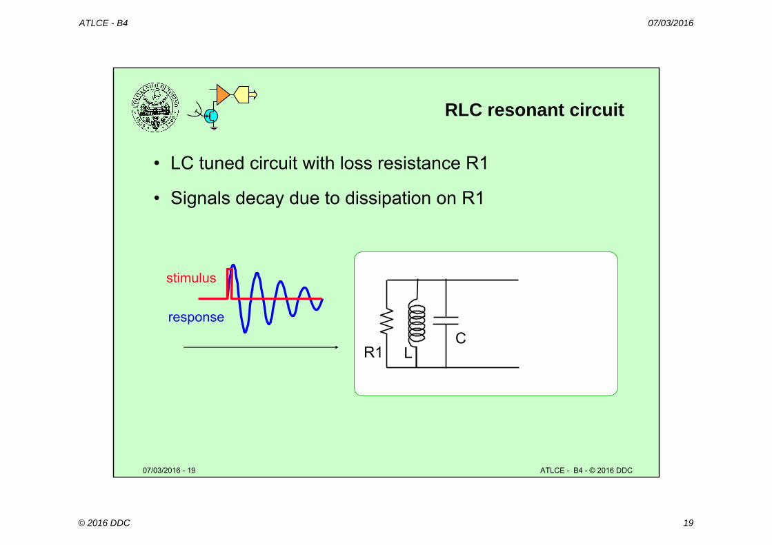
RLC resonant circuit
• LC tuned circuit with loss resistance R1
• Signals decay due to dissipation on R1
R1C
L
stimulus
response
ATLCE - B4 07/03/2016
© 2016 DDC 20
07/03/2016 - 20 ATLCE - B4 - © 2016 DDC
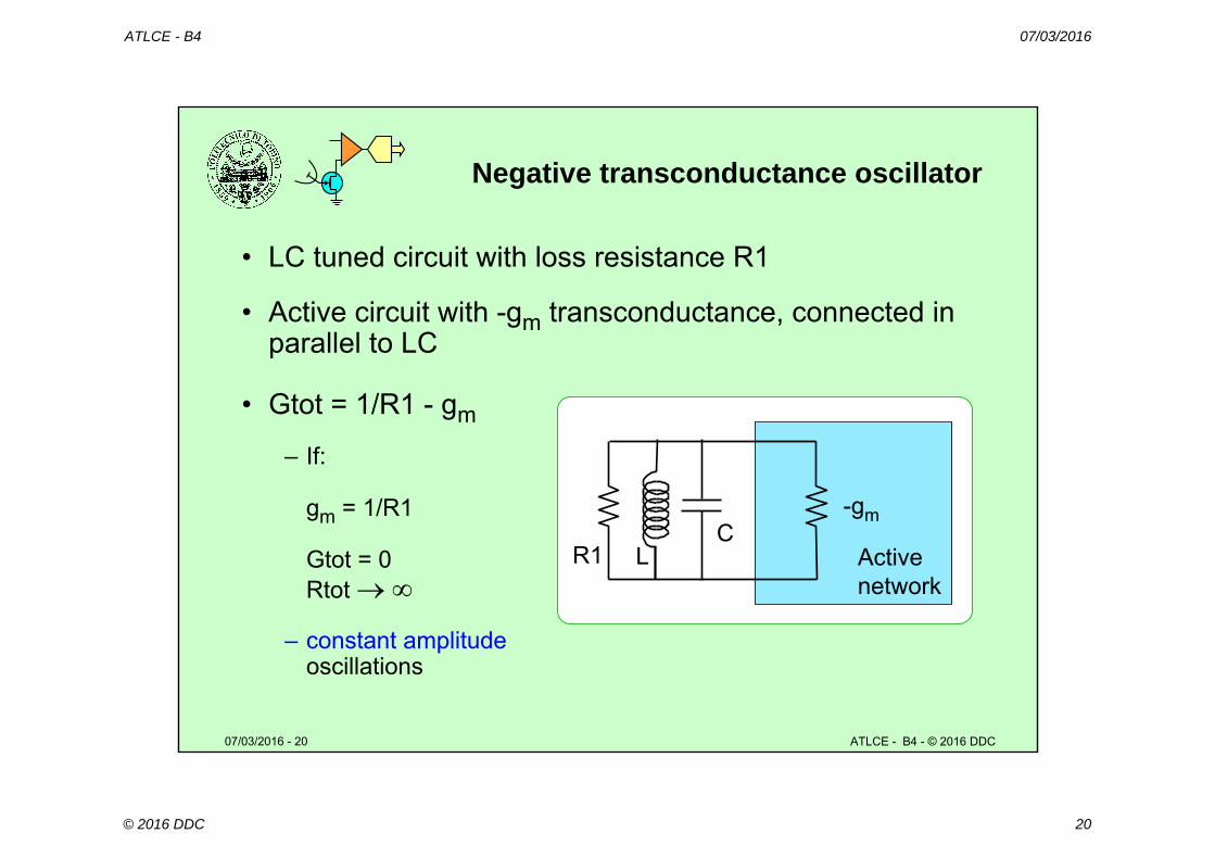
Negative transconductance oscillator
• LC tuned circuit with loss resistance R1
• Active circuit with -gm transconductance, connected in parallel to LC
• Gtot = 1/R1 - gm
– If:
gm = 1/R1
Gtot = 0Rtot
– constant amplitude oscillations
R1C
L
-gm
Active network
ATLCE - B4 07/03/2016
© 2016 DDC 21
07/03/2016 - 21 ATLCE - B4 - © 2016 DDC
Negative transconductance (–gm)
• An active circuit (with gain) is required to get the negative transconductance –gm
– Subject to nonlinearity, distortion, saturation, …
• At startup:– Small signal,
» High gm Rtot < 0» Signal is amplified
• Signal level regulation:– For increasing signal level
» gm, is reduced Rtot becomes positive losses!» Signal is attenuated
– Only stable condition: Rtot = 0
ATLCE - B4 07/03/2016
© 2016 DDC 22
07/03/2016 - 22 ATLCE - B4 - © 2016 DDC
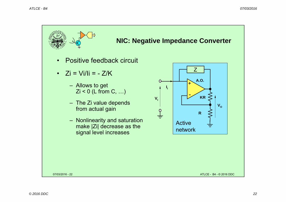
NIC: Negative Impedance Converter
• Positive feedback circuit
• Zi = Vi/Ii = - Z/K
– Allows to get Zi < 0 (L from C, …)
– The Zi value depends from actual gain
– Nonlinearity and saturation make |Zi| decrease as the signal level increases
KR
A.O.
-
+
R
VI
VO
II
Z
Active network
ATLCE - B4 07/03/2016
© 2016 DDC 23
07/03/2016 - 23 ATLCE - B4 - © 2016 DDC
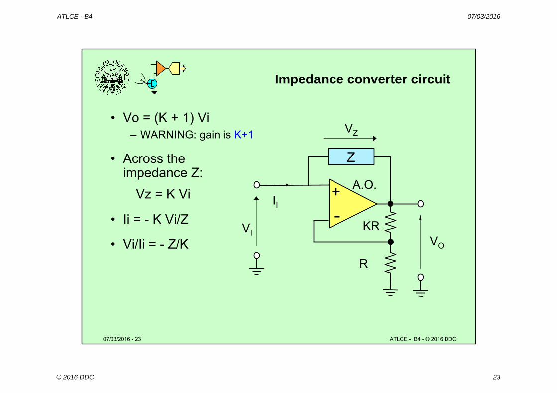
Impedance converter circuit
• Vo = (K + 1) Vi– WARNING: gain is K+1
• Across the impedance Z:
Vz = K Vi
• Ii = - K Vi/Z
• Vi/Ii = - Z/KKR
A.O.
-+
R
VIVO
II
Z
VZ
ATLCE - B4 07/03/2016
© 2016 DDC 24
07/03/2016 - 24 ATLCE - B4 - © 2016 DDC
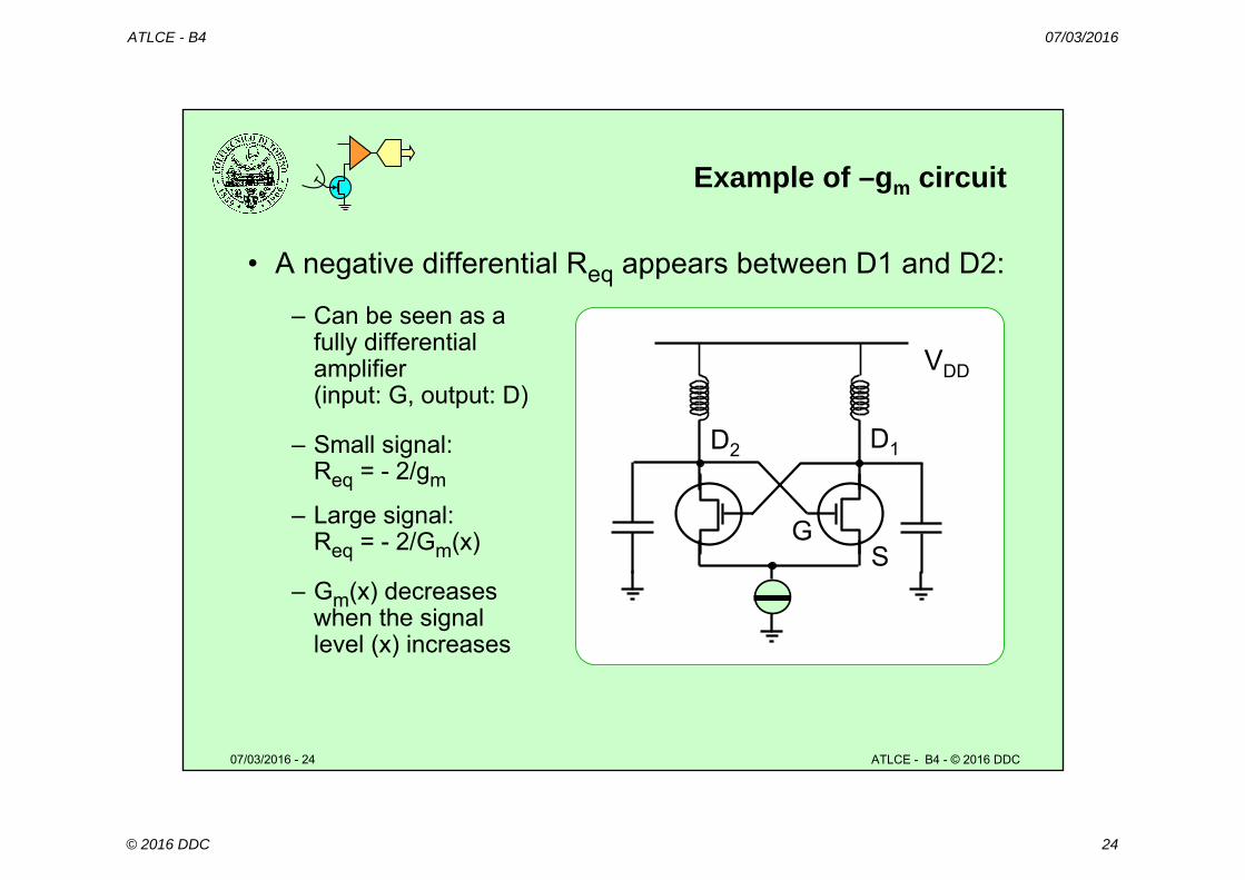
Example of –gm circuit
• A negative differential Req appears between D1 and D2:
– Can be seen as a fully differential amplifier (input: G, output: D)
– Small signal:Req = - 2/gm
– Large signal:Req = - 2/Gm(x)
– Gm(x) decreases when the signal level (x) increases
VDD
S
D1
G
D2
ATLCE - B4 07/03/2016
© 2016 DDC 25
07/03/2016 - 25 ATLCE - B4 - © 2016 DDC
Differential circuits
• The –gm sine source is symmetric (differential)
• Benefits– Constant current sink from the power supply
» The current is deviated to either branch of the differential circuit» Less radiated noise and EMI
– No even harmonics(keeping differential signals)
– Reduced noise sensitivity» The useful signal is differential» Common mode signals are ignored
ATLCE - B4 07/03/2016
© 2016 DDC 26
07/03/2016 - 26 ATLCE - B4 - © 2016 DDC
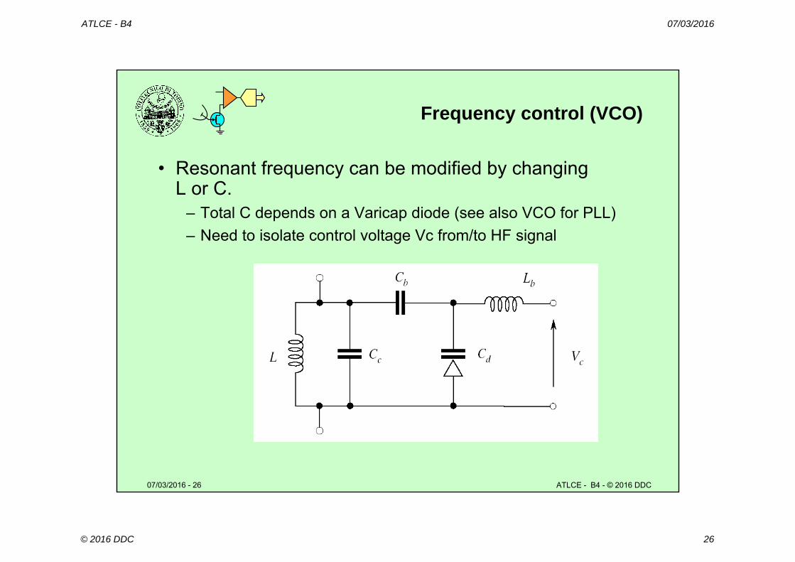
Frequency control (VCO)
• Resonant frequency can be modified by changing L or C.
– Total C depends on a Varicap diode (see also VCO for PLL)– Need to isolate control voltage Vc from/to HF signal
ATLCE - B4 07/03/2016
© 2016 DDC 27
07/03/2016 - 27 ATLCE - B4 - © 2016 DDC
Real circuits and Q
• The resonant circuit Q depends on losses– Loss of L (series Rs) and C (parallel Rp)– The total resistive load on the LC group is the parallel of:
» Input resistance of the following stage» hOE or rD of transistor» Re referred to Vo
• To reduce losses (and raise Q)– Increase parallel Req
» Reactive network» Separation buffer between feedback and load » Use mechanical resonators (with high Q)» Use quartz oscillators
ATLCE - B4 07/03/2016
© 2016 DDC 28
07/03/2016 - 28 ATLCE - B4 - © 2016 DDC
Quartz oscillators
• Quartz is a piezoelectric material– Under mechanical stress generates electrical signals– When receives electrical signals modifies size and shape – The electric-mechanic energy conversion is very efficient at the
(mechanical) resonant frequency
• Quartz crystal = resonator with very high Q– Can be used to build precise and stable oscillators
» By replacing the LC group» With specific circuits (mainly squarewave generators)
• Other resonators use the same techniques (mechanic resonance)
– Ceramic filters, SAW, …
ATLCE - B4 07/03/2016
© 2016 DDC 29
07/03/2016 - 29 ATLCE - B4 - © 2016 DDC
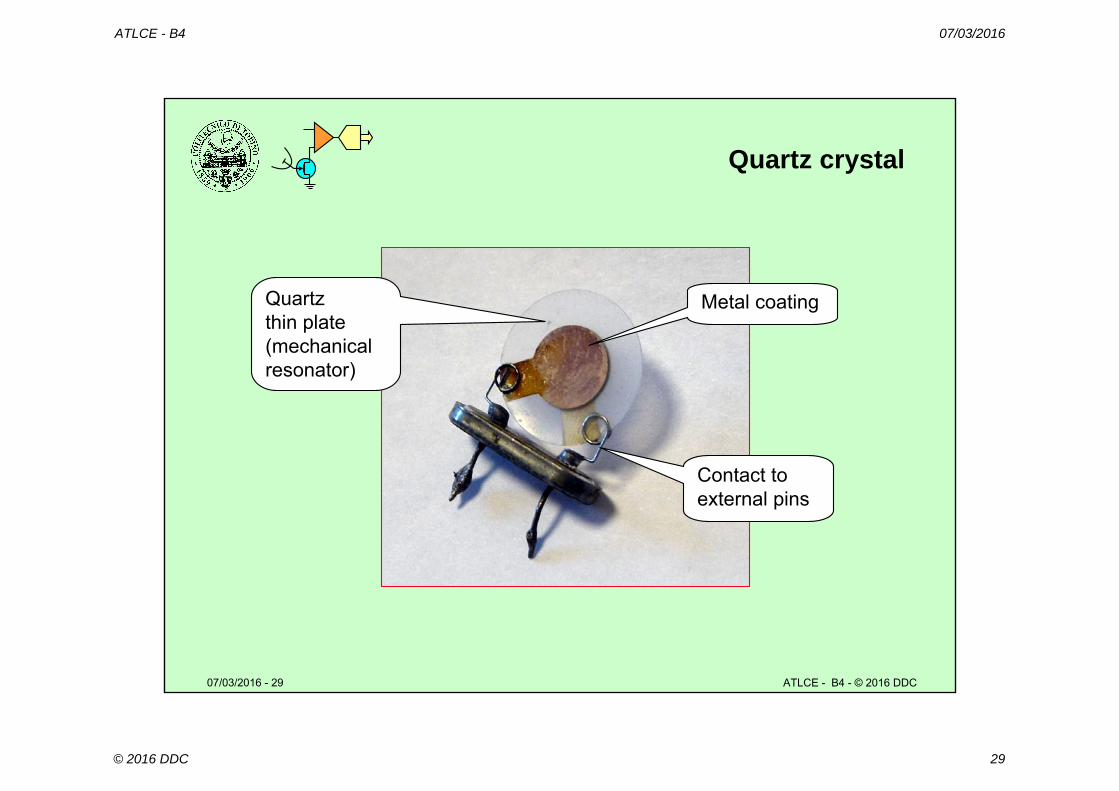
Quartz crystal
Quartzthin plate(mechanicalresonator)
Metal coating
Contact toexternal pins
ATLCE - B4 07/03/2016
© 2016 DDC 30
07/03/2016 - 30 ATLCE - B4 - © 2016 DDC
Lesson B4: final test
• Which parameters describe (completely) a sine signal?
• Draw the block diagram of a single-transistor sine generator.
• How does a NIC work?
• Describe the operation of a NIC-based sine generator.
• Is it possible to build a fixed-amplitude sine generator with fully linear devices?
• Discuss the benefits of differential configurations for signal generators.
• Which are the benefits of quartz oscillators?