Embed Size (px)
Citation preview
TCM8030Analog Baseband Processor
User’s Guide
SLWU002JULY 1997
Printed on Recycled Paper
IMPORTANT NOTICE
Texas Instruments (TI) reserves the right to make changes to its products or to discontinue anysemiconductor product or service without notice, and advises its customers to obtain the latestversion of relevant information to verify, before placing orders, that the information being reliedon is current.
TI warrants performance of its semiconductor products and related software to the specificationsapplicable at the time of sale in accordance with TI’s standard warranty. Testing and other qualitycontrol techniques are utilized to the extent TI deems necessary to support this warranty.Specific testing of all parameters of each device is not necessarily performed, except thosemandated by government requirements.
Certain applications using semiconductor products may involve potential risks of death,personal injury, or severe property or environmental damage (“Critical Applications”).
TI SEMICONDUCTOR PRODUCTS ARE NOT DESIGNED, INTENDED, AUTHORIZED, ORWARRANTED TO BE SUITABLE FOR USE IN LIFE-SUPPORT APPLICATIONS, DEVICESOR SYSTEMS OR OTHER CRITICAL APPLICATIONS.
Inclusion of TI products in such applications is understood to be fully at the risk of the customer.Use of TI products in such applications requires the written approval of an appropriate TI officer.Questions concerning potential risk applications should be directed to TI through a local SCsales office.
In order to minimize risks associated with the customer’s applications, adequate design andoperating safeguards should be provided by the customer to minimize inherent or proceduralhazards.
TI assumes no liability for applications assistance, customer product design, softwareperformance, or infringement of patents or services described herein. Nor does TI warrant orrepresent that any license, either express or implied, is granted under any patent right, copyright,mask work right, or other intellectual property right of TI covering or relating to any combination,machine, or process in which such semiconductor products or services might be or are used.
Copyright 1997, Texas Instruments Incorporated
iii Read This First
Preface
Read This First
About This Manual
This manual provides design information for the TCM8030 analog cellulartelephone baseband processor. The manual is written for senior engineers,junior engineers, and support staff who design and develop analog cellulartelephone baseband processors and applications.
You should be familiar with basic telecommunications concepts, analogtheory, and cellular applications.
How to Use This Manual
This document contains generic and specific information about the TCM8030baseband processor.
Chapter 1 Provides an overview of TCM8030 analog cellular telephonebaseband processing
Chapter 2 Describes the principles that apply during operation of theTCM8030 analog cellular telephone processor
Chapter 3 Describes the receive processing procedure for the forwardcontrol channel (FOCC) and the forward voice channel (FVC)
Chapter 4 Provides AMPS wideband data reverse channel transmissionprocessing procedures for both the reverse control channel (RECC) andreverse voice channel (RVC)
Chapter 5 Describes TCM8030 wideband data transmissions andprovides wideband data transmission examples
Chapter 6 Describes the process and methods used during reverse controlchannel arbitration
Chapter 7 Defines automatic frequency control and its system cycle
Chapter 8 Provides basic information regarding the programmableexpansion input/output ports, special function port keys, and read and writeregister definitions
Related Documentation From Texas Instruments
iv
Chapter 9 Describes the baseband processing techniques to applynecessary external circuitry to the TCM8030
Notational Conventions
An overscored word indicates a signal that is active low.
Words that serve to emphasize an important element, notation, orimperative in a procedure are emphasized in bold .
Related Documentation From Texas Instruments
The following books describe the TCM8030 and related support tools. Toobtain a copy of any of these TI documents, call the Texas InstrumentsLiterature Response Center at (800) 477–8924. When ordering, pleaseidentify the book by its title and literature number.
TCM8030 Analog Baseband Processor Data Manual (literaturenumber SLW033A) describes the component and electrical specificationsfor the TCM8030.
TPS72xx Micropower Low -Dropout (LDO) Voltage Regulators(literature number SLVS102E) describes the components and electricalspecifications for the TPS72xx family.
FCC Warning
This equipment is intended for use in a laboratory test environment only. Itgenerates, uses, and can radiate radio frequency energy and has not beentested for compliance with the limits of computing devices pursuant to subpartJ of part 15 of FCC rules, which are designed to provide reasonable protectionagainst radio frequency interference. Operation of this equipment in otherenvironments may cause interference with radio communications, in whichcase the user at his own expense will be required to take whatever measuresmay be required to correct this interference.
Trademarks
SPI is a trademark of Motorola, Inc.
TI is a trademark of Texas Instruments Incorporated.
If You Need Assistance
v Read This First
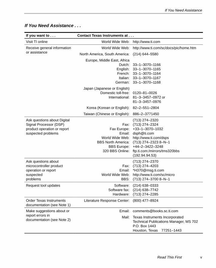
If You Need Assistance . . .
If you want to . . . Contact Texas Instruments at . . .
Visit TI online World Wide Web: http://www.ti.com
Receive general information World Wide Web: http://www.ti.com/sc/docs/pic/home.htmor assistance North America, South America: (214) 644–5580
Europe, Middle East, AfricaDutch:
English:French:Italian:
German:
33–1–3070–116633–1–3070–116533–1–3070–116433–1–3070–116733–1–3070–1168
Japan (Japanese or English)Domestic toll-free:
International:0120–81–002681–3–3457–0972 or81–3–3457–0976
Korea (Korean or English): 82–2–551–2804
Taiwan (Chinese or English): 886–2–3771450
Ask questions about DigitalSignal Processor (DSP)product operation or reportsuspected problems
Fax:Fax Europe:
Email:World Wide Web:
BBS North America:BBS Europe:
320 BBS Online:
(713) 274–2320(713) 274–2324+33–1–3070–[email protected]://www.ti.com/dsps(713) 274–2323 8–N–1+44–2–3422–3248ftp.ti.com:/mirrors/tms320bbs(192.94.94.53)
Ask questions aboutmicrocontroller productoperation or reportsuspected problems
Fax:Email:
World Wide Web:BBS:
(713) 274–2370(713) 274–4203*[email protected]://www.ti.com/sc/micro(713) 274–3700 8–N–1
Request tool updates Software:Software fax:
Hardware:
(214) 638–0333(214) 638–7742(713) 274–2285
Order Texas Instrumentsdocumentation (see Note 1)
Literature Response Center: (800) 477–8924
Make suggestions about or Email: [email protected] errors indocumentation (see Note 2)
Mail: Texas Instruments IncorporatedTechnical Publications Manager, MS 702P.O. Box 1443Houston, Texas 77251–1443
Contents
vii
Contents
1 Introduction 1-1. . . . . . . . . . . . . . . . . . . . . . . . . . . . . . . . . . . . . . . . . . . . . . . . . . . . . . . . . . . . . . . . . . . . . 1.1 Analog Cellular Telephone Baseband Processing 1-2. . . . . . . . . . . . . . . . . . . . . . . . . . . . . . . 1.2 TCM8030 Features 1-3. . . . . . . . . . . . . . . . . . . . . . . . . . . . . . . . . . . . . . . . . . . . . . . . . . . . . . . . .
1.2.1 Data Processing Features 1-3. . . . . . . . . . . . . . . . . . . . . . . . . . . . . . . . . . . . . . . . . . . . 1.2.2 Audio Processing Features 1-3. . . . . . . . . . . . . . . . . . . . . . . . . . . . . . . . . . . . . . . . . . .
1.3 Power Modes 1-4. . . . . . . . . . . . . . . . . . . . . . . . . . . . . . . . . . . . . . . . . . . . . . . . . . . . . . . . . . . . . .
2 Principles of Operation 2-1. . . . . . . . . . . . . . . . . . . . . . . . . . . . . . . . . . . . . . . . . . . . . . . . . . . . . . . . . . 2.1 Principles of Operation Overview 2-2. . . . . . . . . . . . . . . . . . . . . . . . . . . . . . . . . . . . . . . . . . . . . 2.2 Receive Audio Path 2-6. . . . . . . . . . . . . . . . . . . . . . . . . . . . . . . . . . . . . . . . . . . . . . . . . . . . . . . . . 2.3 Transmit Audio Path 2-7. . . . . . . . . . . . . . . . . . . . . . . . . . . . . . . . . . . . . . . . . . . . . . . . . . . . . . . . 2.4 Data Processor 2-9. . . . . . . . . . . . . . . . . . . . . . . . . . . . . . . . . . . . . . . . . . . . . . . . . . . . . . . . . . . . . 2.5 Miscellaneous Circuits 2-11. . . . . . . . . . . . . . . . . . . . . . . . . . . . . . . . . . . . . . . . . . . . . . . . . . . . . 2.6 Clocks 2-12. . . . . . . . . . . . . . . . . . . . . . . . . . . . . . . . . . . . . . . . . . . . . . . . . . . . . . . . . . . . . . . . . . . 2.7 Power Modes 2-15. . . . . . . . . . . . . . . . . . . . . . . . . . . . . . . . . . . . . . . . . . . . . . . . . . . . . . . . . . . . .
2.7.1 Total Power-Down Mode 2-18. . . . . . . . . . . . . . . . . . . . . . . . . . . . . . . . . . . . . . . . . . . . 2.7.2 Shutdown Mode 2-19. . . . . . . . . . . . . . . . . . . . . . . . . . . . . . . . . . . . . . . . . . . . . . . . . . . . 2.7.3 Idle Mode 2-20. . . . . . . . . . . . . . . . . . . . . . . . . . . . . . . . . . . . . . . . . . . . . . . . . . . . . . . . . 2.7.4 Tone Mode 2-20. . . . . . . . . . . . . . . . . . . . . . . . . . . . . . . . . . . . . . . . . . . . . . . . . . . . . . . . 2.7.5 Full Operation Mode, DTMF TX Off 2-20. . . . . . . . . . . . . . . . . . . . . . . . . . . . . . . . . . . 2.7.6 Full Operation Mode, DTMF TX On 2-20. . . . . . . . . . . . . . . . . . . . . . . . . . . . . . . . . . . 2.7.7 Independent Circuits 2-20. . . . . . . . . . . . . . . . . . . . . . . . . . . . . . . . . . . . . . . . . . . . . . . .
2.8 Circuit Definitions 2-21. . . . . . . . . . . . . . . . . . . . . . . . . . . . . . . . . . . . . . . . . . . . . . . . . . . . . . . . . . 2.8.1 Transmit Path Audio Processing Functions 2-21. . . . . . . . . . . . . . . . . . . . . . . . . . . . 2.8.2 Receive Path Audio Processing Functions 2-22. . . . . . . . . . . . . . . . . . . . . . . . . . . . . 2.8.3 Transmit Path Data Processing Functions 2-24. . . . . . . . . . . . . . . . . . . . . . . . . . . . . 2.8.4 Receive Path Data Processing Functions 2-25. . . . . . . . . . . . . . . . . . . . . . . . . . . . . . 2.8.5 Transmit Path SAT Processing Functions 2-26. . . . . . . . . . . . . . . . . . . . . . . . . . . . . . 2.8.6 Receive Path SAT Processing Functions 2-27. . . . . . . . . . . . . . . . . . . . . . . . . . . . . .
2.9 Miscellaneous Functions 2-28. . . . . . . . . . . . . . . . . . . . . . . . . . . . . . . . . . . . . . . . . . . . . . . . . . .
3 Receive Processing 3-1. . . . . . . . . . . . . . . . . . . . . . . . . . . . . . . . . . . . . . . . . . . . . . . . . . . . . . . . . . . . . 3.1 Receive Processing Overview 3-2. . . . . . . . . . . . . . . . . . . . . . . . . . . . . . . . . . . . . . . . . . . . . . . . 3.2 Forward Control Channel (FOCC) Receive Processing 3-4. . . . . . . . . . . . . . . . . . . . . . . . . .
3.2.1 Frame Description 3-4. . . . . . . . . . . . . . . . . . . . . . . . . . . . . . . . . . . . . . . . . . . . . . . . . . . 3.2.2 Synchronization 3-5. . . . . . . . . . . . . . . . . . . . . . . . . . . . . . . . . . . . . . . . . . . . . . . . . . . . .
Table of Contents
viii
3.2.3 Majority Voting 3-5. . . . . . . . . . . . . . . . . . . . . . . . . . . . . . . . . . . . . . . . . . . . . . . . . . . . . . 3.2.4 Normal Operation 3-6. . . . . . . . . . . . . . . . . . . . . . . . . . . . . . . . . . . . . . . . . . . . . . . . . . . 3.2.5 Less Than Five Word Syncs Missing 3-6. . . . . . . . . . . . . . . . . . . . . . . . . . . . . . . . . . . 3.2.6 More Than Five Word Syncs Missing 3-6. . . . . . . . . . . . . . . . . . . . . . . . . . . . . . . . . . . 3.2.7 Single Word Sync Detected 3-7. . . . . . . . . . . . . . . . . . . . . . . . . . . . . . . . . . . . . . . . . . .
3.3 Forward Voice Channel (FVC) Receive Processing 3-8. . . . . . . . . . . . . . . . . . . . . . . . . . . . . 3.3.1 Message Stream 3-8. . . . . . . . . . . . . . . . . . . . . . . . . . . . . . . . . . . . . . . . . . . . . . . . . . . . 3.3.2 Frame Timer 3-8. . . . . . . . . . . . . . . . . . . . . . . . . . . . . . . . . . . . . . . . . . . . . . . . . . . . . . . . 3.3.3 Majority Voting 3-9. . . . . . . . . . . . . . . . . . . . . . . . . . . . . . . . . . . . . . . . . . . . . . . . . . . . . . 3.3.4 Normal Operation 3-9. . . . . . . . . . . . . . . . . . . . . . . . . . . . . . . . . . . . . . . . . . . . . . . . . . . 3.3.5 Less Than Five Word Syncs Missed 3-10. . . . . . . . . . . . . . . . . . . . . . . . . . . . . . . . . . 3.3.6 More Than Five Word Syncs Missed 3-11. . . . . . . . . . . . . . . . . . . . . . . . . . . . . . . . . . 3.3.7 One Word Received 3-11. . . . . . . . . . . . . . . . . . . . . . . . . . . . . . . . . . . . . . . . . . . . . . . .
4 Wideband Data Reverse Channel Transmission Processing 4-1. . . . . . . . . . . . . . . . . . . . . . . . 4.1 Wideband Data Reverse Channel Transmission Processing Overview 4-2. . . . . . . . . . . . . 4.2 Reverse Control Channel Message Stream Description 4-3. . . . . . . . . . . . . . . . . . . . . . . . . . 4.3 Coded Digital Color Code (DCC) 4-4. . . . . . . . . . . . . . . . . . . . . . . . . . . . . . . . . . . . . . . . . . . . . 4.4 RECC Word Format 4-5. . . . . . . . . . . . . . . . . . . . . . . . . . . . . . . . . . . . . . . . . . . . . . . . . . . . . . . . . 4.5 Reverse Voice Channel Message Stream Description 4-6. . . . . . . . . . . . . . . . . . . . . . . . . . . 4.6 RVC Word Format 4-7. . . . . . . . . . . . . . . . . . . . . . . . . . . . . . . . . . . . . . . . . . . . . . . . . . . . . . . . . .
5 Wideband Data Transmission 5-1. . . . . . . . . . . . . . . . . . . . . . . . . . . . . . . . . . . . . . . . . . . . . . . . . . . . 5.1 Wideband Transmission Overview 5-2. . . . . . . . . . . . . . . . . . . . . . . . . . . . . . . . . . . . . . . . . . . . 5.2 Reverse Control Channel (RECC) Wideband Data Transmission 5-3. . . . . . . . . . . . . . . . . .
5.2.1 Setup Procedures 5-3. . . . . . . . . . . . . . . . . . . . . . . . . . . . . . . . . . . . . . . . . . . . . . . . . . . 5.2.2 Write to TX Buffer 5-3. . . . . . . . . . . . . . . . . . . . . . . . . . . . . . . . . . . . . . . . . . . . . . . . . . . 5.2.3 Commence Transmission 5-3. . . . . . . . . . . . . . . . . . . . . . . . . . . . . . . . . . . . . . . . . . . . . 5.2.4 Single-Word Transmission 5-4. . . . . . . . . . . . . . . . . . . . . . . . . . . . . . . . . . . . . . . . . . . . 5.2.5 Multiple-Word Transmission 5-4. . . . . . . . . . . . . . . . . . . . . . . . . . . . . . . . . . . . . . . . . . . 5.2.6 Single-Word Transmission Example 5-6. . . . . . . . . . . . . . . . . . . . . . . . . . . . . . . . . . . . 5.2.7 Multiple-Word Transmission Examples 5-7. . . . . . . . . . . . . . . . . . . . . . . . . . . . . . . . .
5.3 Reverse Voice Channel (RVC) Wideband Data Transmission 5-9. . . . . . . . . . . . . . . . . . . . . 5.3.1 Setup Procedures 5-9. . . . . . . . . . . . . . . . . . . . . . . . . . . . . . . . . . . . . . . . . . . . . . . . . . . 5.3.2 Write to TX Buffer 5-9. . . . . . . . . . . . . . . . . . . . . . . . . . . . . . . . . . . . . . . . . . . . . . . . . . . 5.3.3 Commence Transmission 5-9. . . . . . . . . . . . . . . . . . . . . . . . . . . . . . . . . . . . . . . . . . . . . 5.3.4 Single-Word Transmission 5-10. . . . . . . . . . . . . . . . . . . . . . . . . . . . . . . . . . . . . . . . . . . 5.3.5 Multiple-Word Transmission 5-10. . . . . . . . . . . . . . . . . . . . . . . . . . . . . . . . . . . . . . . . . . 5.3.6 RVC Single-Word Transmission Example 5-11. . . . . . . . . . . . . . . . . . . . . . . . . . . . . . 5.3.7 RVC Multiple-Word Transmission Examples 5-13. . . . . . . . . . . . . . . . . . . . . . . . . . .
5.4 Wideband Data Transmission Precautions 5-15. . . . . . . . . . . . . . . . . . . . . . . . . . . . . . . . . . . .
6 Reverse Control Channel Arbitration Processing 6-1. . . . . . . . . . . . . . . . . . . . . . . . . . . . . . . . . . 6.1 Reverse Control Channel Arbitration Processing Overview 6-2. . . . . . . . . . . . . . . . . . . . . . . 6.2 RECC Arbitration Methods 6-3. . . . . . . . . . . . . . . . . . . . . . . . . . . . . . . . . . . . . . . . . . . . . . . . . . .
Table of Contents
ix Table of Contents
6.2.1 Software Control Arbitration 6-3. . . . . . . . . . . . . . . . . . . . . . . . . . . . . . . . . . . . . . . . . . . 6.2.2 Hardware Control Arbitration 6-3. . . . . . . . . . . . . . . . . . . . . . . . . . . . . . . . . . . . . . . . . . 6.2.3 One or Two Busy/Idle Bits Observed 6-3. . . . . . . . . . . . . . . . . . . . . . . . . . . . . . . . . . .
7 Automatic Frequency Control 7-1. . . . . . . . . . . . . . . . . . . . . . . . . . . . . . . . . . . . . . . . . . . . . . . . . . . . 7.1 Automatic Frequency Control Overview 7-2. . . . . . . . . . . . . . . . . . . . . . . . . . . . . . . . . . . . . . . . 7.2 AFC Reference 7-3. . . . . . . . . . . . . . . . . . . . . . . . . . . . . . . . . . . . . . . . . . . . . . . . . . . . . . . . . . . . . 7.3 AFC System Concept 7-4. . . . . . . . . . . . . . . . . . . . . . . . . . . . . . . . . . . . . . . . . . . . . . . . . . . . . . . 7.4 AFC Sample Cycle Detailed Description 7-5. . . . . . . . . . . . . . . . . . . . . . . . . . . . . . . . . . . . . . .
8 Keyboard Interface and Set Monitoring 8-1. . . . . . . . . . . . . . . . . . . . . . . . . . . . . . . . . . . . . . . . . . . . 8.1 Keyboard Interface and Set Monitoring Overview 8-2. . . . . . . . . . . . . . . . . . . . . . . . . . . . . . . 8.2 Keyboard Interrupt Inputs [KEY3:KEY0] 8-3. . . . . . . . . . . . . . . . . . . . . . . . . . . . . . . . . . . . . . .
8.2.1 PIO Control Word (PIOC3 – Write Address 19H) 8-3. . . . . . . . . . . . . . . . . . . . . . . . . 8.2.2 PIO3 Pullup Enabling (PI3PULL – Write Address 1BH) 8-3. . . . . . . . . . . . . . . . . . . 8.2.3 PIO3 Interrupt Control (PI3INT – Write Address 1CH) 8-3. . . . . . . . . . . . . . . . . . . . 8.2.4 Event Register 2 (E2 – Read Address 06) Bit 6 8-4. . . . . . . . . . . . . . . . . . . . . . . . . .
8.3 TCM8030 8-Bit Programmable Expansion I/O Ports 8-5. . . . . . . . . . . . . . . . . . . . . . . . . . . . . 8.3.1 PIO Control Words (PIOC1 and PIOC2 – Write Address 15H and 17H) 8-5. . . . . 8.3.2 PIO Output Words (PIO1 and PIO2 – Write Address 16H and 18H) 8-5. . . . . . . .
9 Typical Analog Cellular Telephone Processing 9-1. . . . . . . . . . . . . . . . . . . . . . . . . . . . . . . . . . . . . 9.1 Typical Analog Cellular Telephone System Overview 9-2. . . . . . . . . . . . . . . . . . . . . . . . . . . . 9.2 Circuit Description 9-3. . . . . . . . . . . . . . . . . . . . . . . . . . . . . . . . . . . . . . . . . . . . . . . . . . . . . . . . . .
9.2.1 Parts List 9-4. . . . . . . . . . . . . . . . . . . . . . . . . . . . . . . . . . . . . . . . . . . . . . . . . . . . . . . . . . . 9.2.2 Clock and Control 9-4. . . . . . . . . . . . . . . . . . . . . . . . . . . . . . . . . . . . . . . . . . . . . . . . . . . 9.2.3 Transmit Path 9-5. . . . . . . . . . . . . . . . . . . . . . . . . . . . . . . . . . . . . . . . . . . . . . . . . . . . . . . 9.2.4 Receive Path 9-5. . . . . . . . . . . . . . . . . . . . . . . . . . . . . . . . . . . . . . . . . . . . . . . . . . . . . . . 9.2.5 Digital-to-Analog Converters 9-6. . . . . . . . . . . . . . . . . . . . . . . . . . . . . . . . . . . . . . . . . . 9.2.6 Timers 9-6. . . . . . . . . . . . . . . . . . . . . . . . . . . . . . . . . . . . . . . . . . . . . . . . . . . . . . . . . . . . . 9.2.7 Keyboard Scan 9-6. . . . . . . . . . . . . . . . . . . . . . . . . . . . . . . . . . . . . . . . . . . . . . . . . . . . . . 9.2.8 I/O Expansion 9-6. . . . . . . . . . . . . . . . . . . . . . . . . . . . . . . . . . . . . . . . . . . . . . . . . . . . . . .
9.3 Decoupling on Supply Lines 9-7. . . . . . . . . . . . . . . . . . . . . . . . . . . . . . . . . . . . . . . . . . . . . . . . . . 9.4 Decoupling TXVMID and RXVMID 9-8. . . . . . . . . . . . . . . . . . . . . . . . . . . . . . . . . . . . . . . . . . . . 9.5 Microphone Grounding 9-9. . . . . . . . . . . . . . . . . . . . . . . . . . . . . . . . . . . . . . . . . . . . . . . . . . . . . . 9.6 Suggested Trim Adjustment Sequence 9-10. . . . . . . . . . . . . . . . . . . . . . . . . . . . . . . . . . . . . . .
9.6.1 Transmit Adjustment Procedure 9-10. . . . . . . . . . . . . . . . . . . . . . . . . . . . . . . . . . . . . . 9.6.2 Receive Adjustment Procedure 9-11. . . . . . . . . . . . . . . . . . . . . . . . . . . . . . . . . . . . . . . 9.6.3 Muting the Audio Path 9-11. . . . . . . . . . . . . . . . . . . . . . . . . . . . . . . . . . . . . . . . . . . . . . . 9.6.4 RF Stage Adjustment Procedure 9-11. . . . . . . . . . . . . . . . . . . . . . . . . . . . . . . . . . . . .
A Glossary A-1. . . . . . . . . . . . . . . . . . . . . . . . . . . . . . . . . . . . . . . . . . . . . . . . . . . . . . . . . . . . . . . . . . . . . . . .
Figures
x
Figures
1–1 TCM8030 Typical Analog Cellular Processing 1-2. . . . . . . . . . . . . . . . . . . . . . . . . . . . . . . . . . . . . 2–1 TCM8030 Simplified Block Diagram 2-3. . . . . . . . . . . . . . . . . . . . . . . . . . . . . . . . . . . . . . . . . . . . . 2–2 TCM8030 Detailed Functional Block Diagram 2-4. . . . . . . . . . . . . . . . . . . . . . . . . . . . . . . . . . . . . 2–3 Receive Audio Path 2-6. . . . . . . . . . . . . . . . . . . . . . . . . . . . . . . . . . . . . . . . . . . . . . . . . . . . . . . . . . . 2–4 Transmit Audio Path 2-7. . . . . . . . . . . . . . . . . . . . . . . . . . . . . . . . . . . . . . . . . . . . . . . . . . . . . . . . . . . 2–5 Data Processor Block Diagram 2-9. . . . . . . . . . . . . . . . . . . . . . . . . . . . . . . . . . . . . . . . . . . . . . . . . 2–6 Miscellaneous Circuit Block Diagrams 2-11. . . . . . . . . . . . . . . . . . . . . . . . . . . . . . . . . . . . . . . . . . 2–7 Clocking Scheme Functional Block Diagram 2-14. . . . . . . . . . . . . . . . . . . . . . . . . . . . . . . . . . . . . 2–8 Power Modes Block Diagram 2-16. . . . . . . . . . . . . . . . . . . . . . . . . . . . . . . . . . . . . . . . . . . . . . . . . . 3–1 FOCC Frame Format 3-4. . . . . . . . . . . . . . . . . . . . . . . . . . . . . . . . . . . . . . . . . . . . . . . . . . . . . . . . . . 3–2 Simplified FOCC Frame Format 3-4. . . . . . . . . . . . . . . . . . . . . . . . . . . . . . . . . . . . . . . . . . . . . . . . . 3–3 FOCC Normal Operation 3-6. . . . . . . . . . . . . . . . . . . . . . . . . . . . . . . . . . . . . . . . . . . . . . . . . . . . . . . 3–4 FOCC Less Than Five Word Syncs Missing 3-6. . . . . . . . . . . . . . . . . . . . . . . . . . . . . . . . . . . . . . 3–5 FOCC More Than Five Word Syncs Missing 3-7. . . . . . . . . . . . . . . . . . . . . . . . . . . . . . . . . . . . . . 3–6 FOCC Single Word Sync Detected 3-7. . . . . . . . . . . . . . . . . . . . . . . . . . . . . . . . . . . . . . . . . . . . . . 3–7 FVC Message Stream 3-8. . . . . . . . . . . . . . . . . . . . . . . . . . . . . . . . . . . . . . . . . . . . . . . . . . . . . . . . . 3–8 FVC Normal Operation 3-10. . . . . . . . . . . . . . . . . . . . . . . . . . . . . . . . . . . . . . . . . . . . . . . . . . . . . . . 3–9 FVC Less Than Five Word Syncs Missed 3-10. . . . . . . . . . . . . . . . . . . . . . . . . . . . . . . . . . . . . . . 3–10 FVC More Than Five Word Syncs Missed 3-11. . . . . . . . . . . . . . . . . . . . . . . . . . . . . . . . . . . . . . . 3–11 FVC One Word Received 3-12. . . . . . . . . . . . . . . . . . . . . . . . . . . . . . . . . . . . . . . . . . . . . . . . . . . . . 4–1 RECC Message Stream 4-3. . . . . . . . . . . . . . . . . . . . . . . . . . . . . . . . . . . . . . . . . . . . . . . . . . . . . . . 4–2 RECC Word Format 4-5. . . . . . . . . . . . . . . . . . . . . . . . . . . . . . . . . . . . . . . . . . . . . . . . . . . . . . . . . . . 4–3 RVC Message Stream 4-6. . . . . . . . . . . . . . . . . . . . . . . . . . . . . . . . . . . . . . . . . . . . . . . . . . . . . . . . . 4–4 RVC Word Format 4-7. . . . . . . . . . . . . . . . . . . . . . . . . . . . . . . . . . . . . . . . . . . . . . . . . . . . . . . . . . . . 5–1 RECC Message Stream 5-2. . . . . . . . . . . . . . . . . . . . . . . . . . . . . . . . . . . . . . . . . . . . . . . . . . . . . . . 5–2 RVC Message Stream 5-2. . . . . . . . . . . . . . . . . . . . . . . . . . . . . . . . . . . . . . . . . . . . . . . . . . . . . . . . . 5–3 RECC Wideband Data Transmission, Word 1 5-6. . . . . . . . . . . . . . . . . . . . . . . . . . . . . . . . . . . . . 5–4 RECC Wideband Data Transmission, Words 1 and 2 (Multiple-Word Transmission) 5-7. . . 5–5 RECC Wideband Data Transmission, Words 1, 2, and 3 (Multiple-Word Transmission) 5-85–6 RVC Wideband Data Transmission, Word 1 5-12. . . . . . . . . . . . . . . . . . . . . . . . . . . . . . . . . . . . . 5–7 RVC Wideband Data Transmission, Words 1 and 2 (Multiple-Word Transmission) 5-13. . . . 5–8 RVC Wideband Data Transmssion, Words 1, 2, and 3 (Multiple-Word Transmission) 5-14. 6–1 RECC Message Stream (Arbitration) 6-2. . . . . . . . . . . . . . . . . . . . . . . . . . . . . . . . . . . . . . . . . . . . 6–2 FOCC Message Stream 6-2. . . . . . . . . . . . . . . . . . . . . . . . . . . . . . . . . . . . . . . . . . . . . . . . . . . . . . . 7–1 AFC Closed-Loop System Block Diagram 7-4. . . . . . . . . . . . . . . . . . . . . . . . . . . . . . . . . . . . . . . . 7–2 AFC Diagram 7-6. . . . . . . . . . . . . . . . . . . . . . . . . . . . . . . . . . . . . . . . . . . . . . . . . . . . . . . . . . . . . . . . .
Figures
xi Table of Contents
8–1 TCM8030 Keyboard and Microcontroller Interface 8-2. . . . . . . . . . . . . . . . . . . . . . . . . . . . . . . . . 9–1 Typical Analog Cellular Telephone System 9-2. . . . . . . . . . . . . . . . . . . . . . . . . . . . . . . . . . . . . . . 9–2 Analog Cellular Telephone Baseband Schematic 9-3. . . . . . . . . . . . . . . . . . . . . . . . . . . . . . . . . . 9–3 Decoupling TXVMID and RXVMID 9-8. . . . . . . . . . . . . . . . . . . . . . . . . . . . . . . . . . . . . . . . . . . . . . 9–4 Microphone Grounding 9-9. . . . . . . . . . . . . . . . . . . . . . . . . . . . . . . . . . . . . . . . . . . . . . . . . . . . . . . .
Tables
xii
Tables
2–1 Clock Sources 2-12. . . . . . . . . . . . . . . . . . . . . . . . . . . . . . . . . . . . . . . . . . . . . . . . . . . . . . . . . . . . . . . 2–2 Master Clock Input Frequency and CLKOUT Select 2-13. . . . . . . . . . . . . . . . . . . . . . . . . . . . . . 2–3 Power Modes Block Diagram Legend 2-15. . . . . . . . . . . . . . . . . . . . . . . . . . . . . . . . . . . . . . . . . . . 3–1 Read/Write Address Information for Receive Processing 3-2. . . . . . . . . . . . . . . . . . . . . . . . . . . 4–1 Coded Digital Color Code 4-4. . . . . . . . . . . . . . . . . . . . . . . . . . . . . . . . . . . . . . . . . . . . . . . . . . . . . . 5–1 Setup Procedures for Wide-Band Data Transmission on RECC 5-3. . . . . . . . . . . . . . . . . . . . . 5–2 Write to TX Buffer 5-3. . . . . . . . . . . . . . . . . . . . . . . . . . . . . . . . . . . . . . . . . . . . . . . . . . . . . . . . . . . . . 5–3 Commence Transmission 5-4. . . . . . . . . . . . . . . . . . . . . . . . . . . . . . . . . . . . . . . . . . . . . . . . . . . . . . 5–4 Write to TX Buffer 5-5. . . . . . . . . . . . . . . . . . . . . . . . . . . . . . . . . . . . . . . . . . . . . . . . . . . . . . . . . . . . . 5–5 Setup Procedures for Wideband Data Transmission on RVC 5-9. . . . . . . . . . . . . . . . . . . . . . . . 5–6 Write to TX Buffer 5-9. . . . . . . . . . . . . . . . . . . . . . . . . . . . . . . . . . . . . . . . . . . . . . . . . . . . . . . . . . . . . 5–7 Commence Transmission 5-10. . . . . . . . . . . . . . . . . . . . . . . . . . . . . . . . . . . . . . . . . . . . . . . . . . . . . 5–8 Write to TX Buffer 5-11. . . . . . . . . . . . . . . . . . . . . . . . . . . . . . . . . . . . . . . . . . . . . . . . . . . . . . . . . . . . 7–1 AFC 20-Bit Terminal Count Read Address Control Execution 7-7. . . . . . . . . . . . . . . . . . . . . . . 8–1 PIO Control Word – PIOC3 8-3. . . . . . . . . . . . . . . . . . . . . . . . . . . . . . . . . . . . . . . . . . . . . . . . . . . . . 8–2 PIO3 Interrupt Control (PI3INT, Bits 3–0) Definition 8-3. . . . . . . . . . . . . . . . . . . . . . . . . . . . . . . . 8–3 PIO3 Interrupt Control (PI3INT, Bits 7–4) Definition 8-4. . . . . . . . . . . . . . . . . . . . . . . . . . . . . . . . 8–4 PIO Control Words – PIOC1 and PIOC2 8-5. . . . . . . . . . . . . . . . . . . . . . . . . . . . . . . . . . . . . . . . . 9–1 Analog Cellular Telephone Components List 9-4. . . . . . . . . . . . . . . . . . . . . . . . . . . . . . . . . . . . . . 9–2 Typical Tranmsit Signal Levels AMPS Mode (3-V Operation) 9-12. . . . . . . . . . . . . . . . . . . . . . . 9–3 Typical Transmit Signal Levels NAMPS Mode (3-V Operation) 9-12. . . . . . . . . . . . . . . . . . . . . 9–4 Typical Transmit Signal Levels TACS Mode (3-V Operation) 9-13. . . . . . . . . . . . . . . . . . . . . . . 9–5 Typical Transmit Signal Levels NTACS Mode (3-V Operation) 9-13. . . . . . . . . . . . . . . . . . . . . . 9–6 Typical Receive Signal Levels AMPS Mode (3-V Operation) 9-13. . . . . . . . . . . . . . . . . . . . . . . 9–7 Typical Receive Signal Levels NAMPS Mode (3-V Operation) 9-14. . . . . . . . . . . . . . . . . . . . . . 9–8 Typical Receive Signal Levels TACS Mode (3-V Operation) 9-14. . . . . . . . . . . . . . . . . . . . . . . . 9–9 Typical Receive Signal Levels NTACS Mode (3-V Operation) 9-14. . . . . . . . . . . . . . . . . . . . . .
1-1
Introduction
This chapter provides an overview of TCM8030 analog cellular telephonebaseband processing. It describes TCM8030 features and the power modesused in generic and specific processing applications, as detailed in laterchapters.
Topic Page
1.1 Analog Cellular Telephone Baseband Processing 1-2. . . . . . . . . . . . . . . .
1.2 TCM8030 Features 1-3. . . . . . . . . . . . . . . . . . . . . . . . . . . . . . . . . . . . . . . . . . . .
1.3 Power Modes 1-4. . . . . . . . . . . . . . . . . . . . . . . . . . . . . . . . . . . . . . . . . . . . . . . . .
Chapter 1
Analog Cellular Telephone Baseband Processing
1-2
1.1 Analog Cellular Telephone Baseband Processing
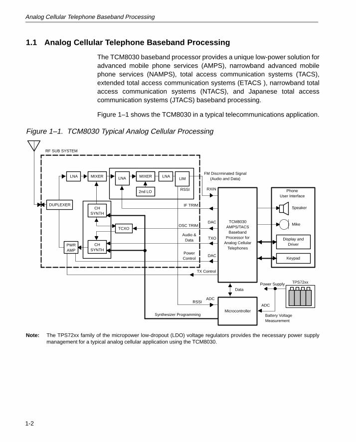
The TCM8030 baseband processor provides a unique low-power solution foradvanced mobile phone services (AMPS), narrowband advanced mobilephone services (NAMPS), total access communication systems (TACS),extended total access communication systems (ETACS ), narrowband totalaccess communication systems (NTACS), and Japanese total accesscommunication systems (JTACS) baseband processing.
Figure 1–1 shows the TCM8030 in a typical telecommunications application.
Figure 1–1. TCM8030 Typical Analog Cellular Processing
TCM8030AMPS/TACS
BasebandProcessor for
Analog CellularTelephones
PhoneUser Interface
Speaker
Display andDriver
Mike
Keypad
Microcontroller
Power Supply
ADC
Battery VoltageMeasurement
Data
LNA MIXER LNA MIXERMIXER
2nd LO
LNALIM
DUPLEXER
RSSI
CHSYNTH
CHSYNTH
TCXO
PWRAMP
FM Discrminated Signal(Audio and Data)
RF SUB SYSTEM
RXIN
IF TRIM
OSC TRIM
Audio &Data
PowerControl
TX Control
DAC
TXO
DAC
RSSI
Synthesizer Programming
ADC
TPS72xx
Note: The TPS72xx family of the micropower low-dropout (LDO) voltage regulators provides the necessary power supplymanagement for a typical analog cellular application using the TCM8030.
TCM8030 Features
1-3Introduction
1.2 TCM8030 Features
The TCM8030 provides all data and audio processing functions for AMPS,NAMPS, TACS, ETACS, NTACS, and JTACS in a compact, low-power,baseband processor enclosed in an 80-pin TQFP package.
1.2.1 Data Processing Features
The TCM8030 provides data transceiver, data processing, and supervisoryaudio tone (SAT) functions, and includes the following data processingfeatures:
Single-chip processing for AMPS, NAMPS, TACS, ETACS, NTACS,JTACS, SAT, and digital supervisory audio tone (DSAT)
2.7-V to 5.5-V operation Serial interface User-configurable interrupt structure Transmit (TX) and receive (RX) data buffers Integrated RX and TX data filters TX wideband (WB) SAT filter RX WB and narrowband (NB) SAT filters RX WB and NB data comparator Programmable timer Independent watchdog timer RX/TX automatic mute functions Arbitration processing Twenty programmable expansion I/O ports WB and NB-RX recovery Automatic frequency control (AFC) Multiple power-saving mode implementation Separate encoder for WB-TX and NB-TX
1.2.2 Audio Processing Features
The TCM8030 provides the following audio processing features:
AMPS, NAMPS, TACS, ETACS, NTACS, and JTACS operation Integrated RX and TX voice filters Microphone amplifiers and loud speaker drivers Pre-emphasis and de-emphasis filtering Digitally-controlled gains and signal selection or muting Adjustable TX limiter Three 8-bit digital-to-analog converters (DAC) with output buffers Dual-tone multifrequency (DTMF) generator On-chip compandor Flexible clock and oscillator operation
Power Modes
1-4
1.3 Power Modes
The TCM8030 power mode structure provides independent powering ofvarious on-chip circuits, thereby enabling the creation of low-power designsthat are ideal for frequency modulation (FM) analog cellular telephones. Thepower modes are as follows:
Total power-down mode Shutdown mode Idle mode Tonemode Full operation (DTMF TX off) mode Full operation (DTMF TX on) mode
2-1
Principles of Operation
This chapter describes the principles that apply during operation of theTCM8030 analog cellular telephone processor.
Topic Page
2.1 Principles of Operation Overview 2-2. . . . . . . . . . . . . . . . . . . . . . . . . . . . . . .
2.2 Receive Audio Path 2-6. . . . . . . . . . . . . . . . . . . . . . . . . . . . . . . . . . . . . . . . . . .
2.3 Transmit Audio Path 2-7. . . . . . . . . . . . . . . . . . . . . . . . . . . . . . . . . . . . . . . . . .
2.4 Data Processor 2-9. . . . . . . . . . . . . . . . . . . . . . . . . . . . . . . . . . . . . . . . . . . . . . .
2.5 Miscellaneous Circuits 2-11. . . . . . . . . . . . . . . . . . . . . . . . . . . . . . . . . . . . . . .
2.6 Clocks 2-12. . . . . . . . . . . . . . . . . . . . . . . . . . . . . . . . . . . . . . . . . . . . . . . . . . . . . .
2.7 Power Modes 2-15. . . . . . . . . . . . . . . . . . . . . . . . . . . . . . . . . . . . . . . . . . . . . . . .
2.8 Circuit Definitions 2-21. . . . . . . . . . . . . . . . . . . . . . . . . . . . . . . . . . . . . . . . . . . .
2.9 Miscellaneous Functions 2-28. . . . . . . . . . . . . . . . . . . . . . . . . . . . . . . . . . . . .
Chapter 2
Principles of Operation Overview
2-2
2.1 Principles of Operation Overview
The TCM8030 provides a complete, low-power, integrated solution for FManalog cellular telephones by integrating the analog processing and digitaldata processing functions onto one chip.
The TCM8030 contains transmit (TX) and receive (RX) analog paths, a digitaldata processor with filters, a compressor and expandor, routing switches, datainput/output (I/O), an audio power amplifier, an uncommitted operationalamplifier, and a DTMF generator. With these circuits, the TCM8030 appliesappropriate signal levels for AMPS, NAMPS, TACS, ETACS, JTACS, andNTACS standards. In addition, both analog paths are software configurablesuch that all audio trimming functions can be achieved without manualintervention.
The TCM8030 data processor has several functional features: it performstransmit encoding and receive decoding, as well as majority voting and datarecovery; it generates supervisory audio tone (SAT) and digital supervisoryaudio tone (DSAT); and it implements a number of independent circuits forarbitration logic, timers, and power logic. These features, along with a simpleserial peripheral interface (SPI ) that interfaces with an externalmicrocontroller, make the TCM8030 data processor extremely effective for allof the analog standards.
The TCM8030 provides greater integration than typical analog cellularbaseband systems; thus, it reduces power consumption and increases talkand standby time. This integration, along with the other TCM8030 features,offers an efficient and effective cost solution for FM analog telephones andrelated applications.
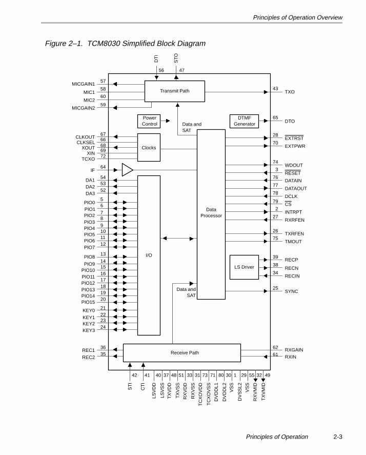
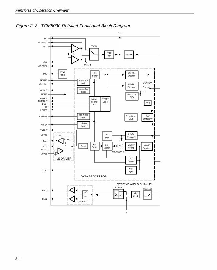
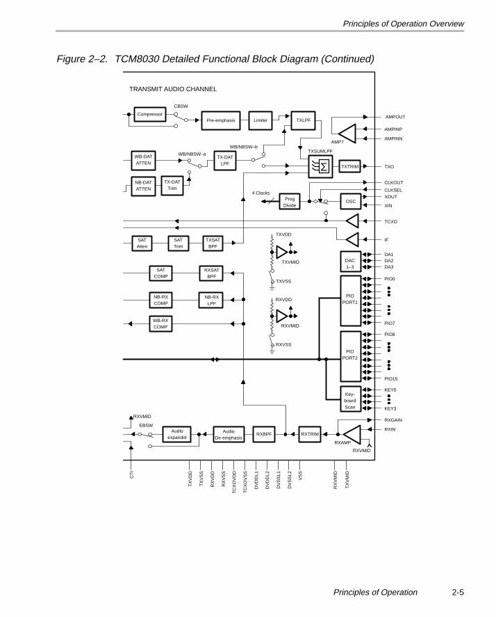
Figure 2–1 shows a simplified block diagram of the device, and Figure 2–2shows a detailed functional block diagram of the device.
Principles of Operation Overview
2-3Principles of Operation
Transmit Path
PowerControl
DataProcessor
DTMFGenerator
LS Driver
Clocks
I/O
Receive Path
42
ST
I
CT
I
LSV
DD
40
LSV
SS
41
TX
VD
D
TX
VS
S
RX
VD
D
RX
VS
S
TC
XO
VD
D
TC
XO
VS
S
DV
DD
L1
DV
DD
L2
VS
S
DV
SS
L2
VS
S
RX
VM
ID
TX
VM
ID
37 48 51 33 31 73 71 80 30 1 29 55 32 49
57
58
60
59
6766686972
64
545352
56
78
9101112
13
14151617181920
21222324
3635
43
65
28
70
74
3
76
77
78
79
2
27
26
75
39
38
34
25
62
61
56 47
DT
I
ST
O
MICGAIN1
TXOMIC1
MIC2
MICGAIN2
CLKOUTCLKSEL
XOUTXIN
TCXO
IF
DA1DA2DA3
PIO0PIO1PIO2PIO3PIO4PIO5PIO6PIO7
PIO8
PIO9PIO10PIO11PIO12PIO13PIO14PIO15
KEY0
KEY1KEY2KEY3
REC1
REC2
DTO
EXTRST
EXTPWR
WDOUT
RESET
DATAIN
DATAOUT
DCLK
CS
INTRPT
RXRFEN
TXRFEN
TMOUT
RECP
RECN
RECIN
SYNC
RXGAIN
RXIN
Data andSAT
Data andSAT
Figure 2–1. TCM8030 Simplified Block Diagram
Principles of Operation Overview
2-4
Figure 2–2. TCM8030 Detailed Functional Block Diagram
ÎÎÎÎÎÎ
ÎÎÎÎÎÎÎÎÎÎÎÎ
Σ
Power-OffLogic
ÎÎÎÎ
V/DTrim
TXBPF
WB-TXEncoder
NB-TXEncoder
DSAT/DSTGEN
DSATSW
TXBuffer
Micro-control
I/F
INTRPTLogic ÏÏ
ÏÏ
WatchdogTimer
RXBuffer
LS DRIVER
BCHDecoder
DSATDET
MajorityVoting
NB-RXRecovery
Sync WordDET
WB-RXRecovery
SATGEN/DET
ÎÎÎÎÎÎ
REC1SW
VOLCTRL
RECSUM
DTI
ST
I
STO
MICGAIN1
MIC1
MIC2
MICGAIN2
DTO
EXTRST
EXTPWR
ÌÌÌÌÌÌ
WDOUT
RESET
DATAINDATAOUT
DCLKCS
INTRPT
RXRFEN
TXRFEN
TMOUT
LSVDD
RECP
RECN
LSVSS
RECIN
SYNC
REC1
REC2
TXSW
WB/NBSW–c
RECEIVE AUDIO CHANNEL
DATA PROCESSOR
TXVMID
DTMFGEN
AFC
RECBUF
ÎÎÎÎÎÎ
Timer
RXControl
WordSync
Idle-ModeLogic
ArbitratLogic
Principles of Operation Overview
2-5Principles of Operation
Figure 2–2. TCM8030 Detailed Functional Block Diagram (Continued)
Compressor
CBSW
Pre-emphasis Limiter TXLPF
ΣTX-DAT
LPF
WB/NBSW–aWB-DATATTEN
TX-DATTrim
NB-DATATTEN
SATAtten
SATTrim
TXSATBPF
RXSATBPF
SATCOMP
NB-RXLPF
NB-RXCOMP
WB-RXCOMP
TXVMID
RXVMID
TXTRIM
ÏÏÏÏ
ÏÏÏÏTXSUMLPF
ÏÏÏÏ
DAC1–3
AMP7
4 Clocks
RXAMP
RXTRIMRXBPFAudio
expandor
EBSW
AMPOUT
AMPINP
AMPINN
TXO
CLKOUT
CLKSELXOUT
XIN
TCXO
IF
DA1DA2DA3
PIO0
PIO7
PIO8
PIO15
KEY0
KEY3
RXGAIN
RXIN
TX
VM
ID
RX
VM
ID
VS
S
DV
SS
L2
DV
SS
L1
DV
DD
L2
DV
DD
L1
TC
XO
VS
S
TC
XO
VD
D
RX
VS
S
RX
VD
D
TX
VS
S
TX
VD
D
CT
I
WB/NBSW–b
AudioDe-emphasis
TRANSMIT AUDIO CHANNEL
RXVMID
RXVMID
TXVDD
TXVSS
RXVDD
RXVSS
ProgDivide
OSC
PIOPORT1
PIOPORT2
Key-boardScan
Receive Audio Path
2-6
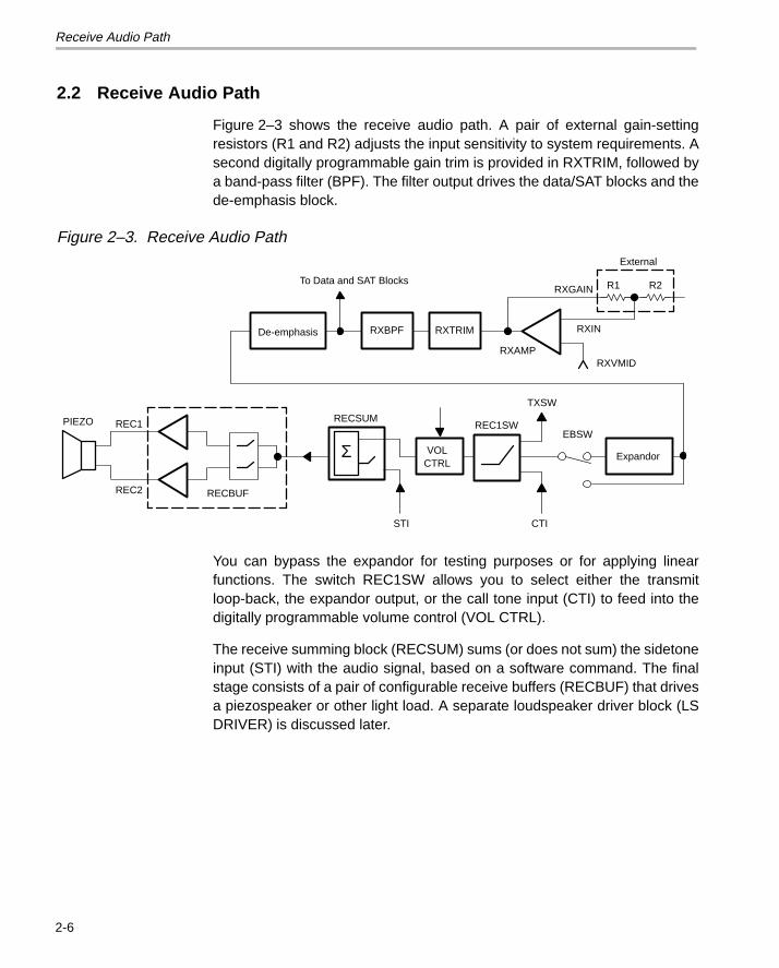
2.2 Receive Audio Path
Figure 2–3 shows the receive audio path. A pair of external gain-settingresistors (R1 and R2) adjusts the input sensitivity to system requirements. Asecond digitally programmable gain trim is provided in RXTRIM, followed bya band-pass filter (BPF). The filter output drives the data/SAT blocks and thede-emphasis block.
Figure 2–3. Receive Audio Path
RXAMP
RXTRIMRXBPF
Expandor
REC1SWEBSW
VOLCTRL
Σ
RECSUM
RECBUF
RXGAIN
RXINDe-emphasis
R1 R2
REC1
REC2
PIEZO
STI CTI
To Data and SAT Blocks
TXSW
RXVMID
External
You can bypass the expandor for testing purposes or for applying linearfunctions. The switch REC1SW allows you to select either the transmitloop-back, the expandor output, or the call tone input (CTI) to feed into thedigitally programmable volume control (VOL CTRL).
The receive summing block (RECSUM) sums (or does not sum) the sidetoneinput (STI) with the audio signal, based on a software command. The finalstage consists of a pair of configurable receive buffers (RECBUF) that drivesa piezospeaker or other light load. A separate loudspeaker driver block (LSDRIVER) is discussed later.
Transmit Audio Path
2-7Principles of Operation
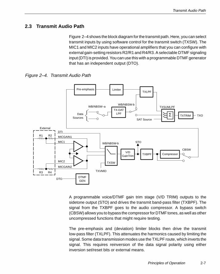
2.3 Transmit Audio Path
Figure 2–4 shows the block diagram for the transmit path. Here, you can selecttransmit inputs by using software control for the transmit switch (TXSW). TheMIC1 and MIC2 inputs have operational amplifiers that you can configure withexternal gain-setting resistors R2/R1 and R4/R3. A selectable DTMF signalinginput (DTI) is provided. You can use this with a programmable DTMF generatorthat has an independent output (DTO).
Figure 2–4. Transmit Audio Path
V/DGainTrim TXBPF Compressor
CBSW
Pre-emphasis LimiterTXLPF
ΣTX-DAT
LPFTXTRIM
TXSUMLPF
DTI
STO
MICGAIN1
MIC1
MIC2
MICGAIN2
DTODTMFGEN
WB/NBSW-b
R1 R2
R3 R4
DataSources
WB/NBSW–a
SAT SourceTXO
TXVMID
External
WB/NBSW-b
TXSW
A programmable voice/DTMF gain trim stage (V/D TRIM) outputs to thesidetone output (STO) and drives the transmit band-pass filter (TXBPF). Thesignal from the TXBPF goes to the audio compressor. A bypass switch(CBSW) allows you to bypass the compressor for DTMF tones, as well as otheruncompressed functions that might require testing.
The pre-emphasis and (deviation) limiter blocks then drive the transmitlow-pass filter (TXLPF). This attenuates the harmonics caused by limiting thesignal. Some data transmission modes use the TXLPF route, which inverts thesignal. This requires reinversion of the data signal polarity using eitherinversion set/reset bits or external means.
Transmit Audio Path
2-8
The transmit summer and low-pass filter block (TXSUMLPF) selects voice,data, or SAT signals and sums them together. It also provides a continuous-time smoothing filter that removes high-frequency products. The transmitgain-trim (TXTRIM) is the final stage that drives the output terminal (TXO).
Data Processor
2-9Principles of Operation
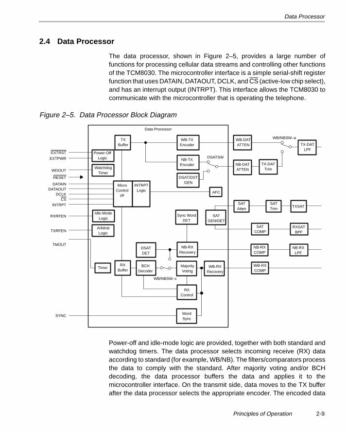
2.4 Data Processor
The data processor, shown in Figure 2–5, provides a large number offunctions for processing cellular data streams and controlling other functionsof the TCM8030. The microcontroller interface is a simple serial-shift registerfunction that uses DATAIN, DATAOUT, DCLK, and CS (active-low chip select),and has an interrupt output (INTRPT). This interface allows the TCM8030 tocommunicate with the microcontroller that is operating the telephone.
Figure 2–5. Data Processor Block Diagram
WB-TXEncoder
NB-TXEncoder
DSAT/DSTGEN
DSATSW
TXBuffer
MicroControl
I/F
INTRPTLogic AFC
Power-OffLogic
WatchdogTimer
Idle-ModeLogic
ArbitratLogic
RXBuffer
Timer BCHDecoder
DSATDET
MajorityVoting
NB-RXRecovery
Sync WordDET
WB-RXRecovery
SATGEN/DET
RXControl
WordSync
WB/NBSW–c
TX-DATLPF
WB/NBSW–aWB-DATATTEN
TX-DATTrim
NB-DATATTEN
SATAtten
SATTrim
TXSAT
RXSATBPF
SATCOMP
NB-RXLPF
NB-RXCOMP
WB-RXCOMP
Data Processor
EXTRST
EXTPWR
WDOUT
RESET
DATAINDATAOUT
DCLKCS
INTRPT
RXRFEN
TXRFEN
TMOUT
SYNC
Power-off and idle-mode logic are provided, together with both standard andwatchdog timers. The data processor selects incoming receive (RX) dataaccording to standard (for example, WB/NB). The filters/comparators processthe data to comply with the standard. After majority voting and/or BCHdecoding, the data processor buffers the data and applies it to themicrocontroller interface. On the transmit side, data moves to the TX bufferafter the data processor selects the appropriate encoder. The encoded data
Data Processor
2-10
goes through the attenuator and/or trim stage to the transmit data low-passfilter (TX-DAT LPF) and switches to the transmit (TX) audio path.
The RXSAT filter and SAT comparator recover the SAT (supervisory audiotone) from the receive audio path and feed it to the data processor detector/generator. The SAT GEN/DET block generates TXSAT and applies it throughprogrammable attenuator/trim stages to the band-pass filter that feeds thetransmit path.
The NB data recovery block detects a DSAT (digital supervisory audio tone)signal. The DSAT/DST GEN regenerates the DSAT signal and sends itthrough the normal NB-DAT path to the transmit path.
Miscellaneous Circuits
2-11Principles of Operation
2.5 Miscellaneous Circuits
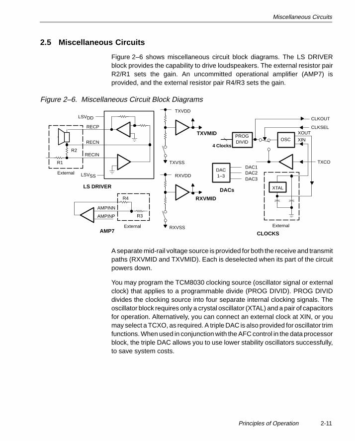
Figure 2–6 shows miscellaneous circuit block diagrams. The LS DRIVERblock provides the capability to drive loudspeakers. The external resistor pairR2/R1 sets the gain. An uncommitted operational amplifier (AMP7) isprovided, and the external resistor pair R4/R3 sets the gain.
Figure 2–6. Miscellaneous Circuit Block Diagrams
LSVDD
LSVSS
RECP
RECN
RECIN
LS DRIVER
AMPINN
AMPINP
R4
R3
AMP7
R1
R2
TXVMID
RXVMID
PROGDIVID OSC
CLKOUT
CLKSELXOUT
XIN
TXCO
XTAL
DAC1–3
DAC1
DAC3DAC2
CLOCKS
DACs
4 Clocks
TXVDD
TXVSS
RXVDD
RXVSS ExternalExternal
External
A separate mid-rail voltage source is provided for both the receive and transmitpaths (RXVMID and TXVMID). Each is deselected when its part of the circuitpowers down.
You may program the TCM8030 clocking source (oscillator signal or externalclock) that applies to a programmable divide (PROG DIVID). PROG DIVIDdivides the clocking source into four separate internal clocking signals. Theoscillator block requires only a crystal oscillator (XTAL) and a pair of capacitorsfor operation. Alternatively, you can connect an external clock at XIN, or youmay select a TCXO, as required. A triple DAC is also provided for oscillator trimfunctions. When used in conjunction with the AFC control in the data processorblock, the triple DAC allows you to use lower stability oscillators successfully,to save system costs.
Clocks
2-12
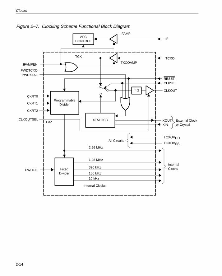
2.6 Clocks
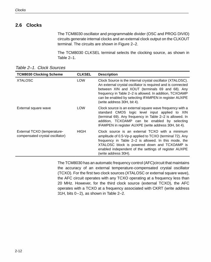
The TCM8030 oscillator and programmable divider (OSC and PROG DIVID)circuits generate internal clocks and an external clock output on the CLKOUTterminal. The circuits are shown in Figure 2–2.
The TCM8030 CLKSEL terminal selects the clocking source, as shown inTable 2–1.
Table 2–1. Clock Sources
TCM8030 Clocking Scheme CLKSEL Description
XTALOSC LOW Clock Source is the internal crystal oscillator (XTALOSC).An external crystal oscillator is required and is connectedbetween XIN and XOUT (terminals 69 and 68). Anyfrequency in Table 2–2 is allowed. In addition, TCXOAMPcan be enabled by selecting IFAMPEN in register AUXPE(write address 30H, bit 4).
External square wave LOW Clock source is an external square wave frequency with astandard CMOS logic level input applied to XIN(terminal 69). Any frequency in Table 2–2 is allowed. Inaddition, TCXOAMP can be enabled by selectingIFAMPEN in register AUXPE (write address 30H, bit 4).
External TCXO (temperature-compensated crystal oscillator)
HIGH Clock source is an external TCXO with a minimumamplitude of 0.5-Vp-p applied to TCXO (terminal 72). Anyfrequency in Table 2–2 is allowed. In this mode, theXTALOSC block is powered down and TCXOAMP isenabled independent of the settings of register AUXPE(write address 30H).
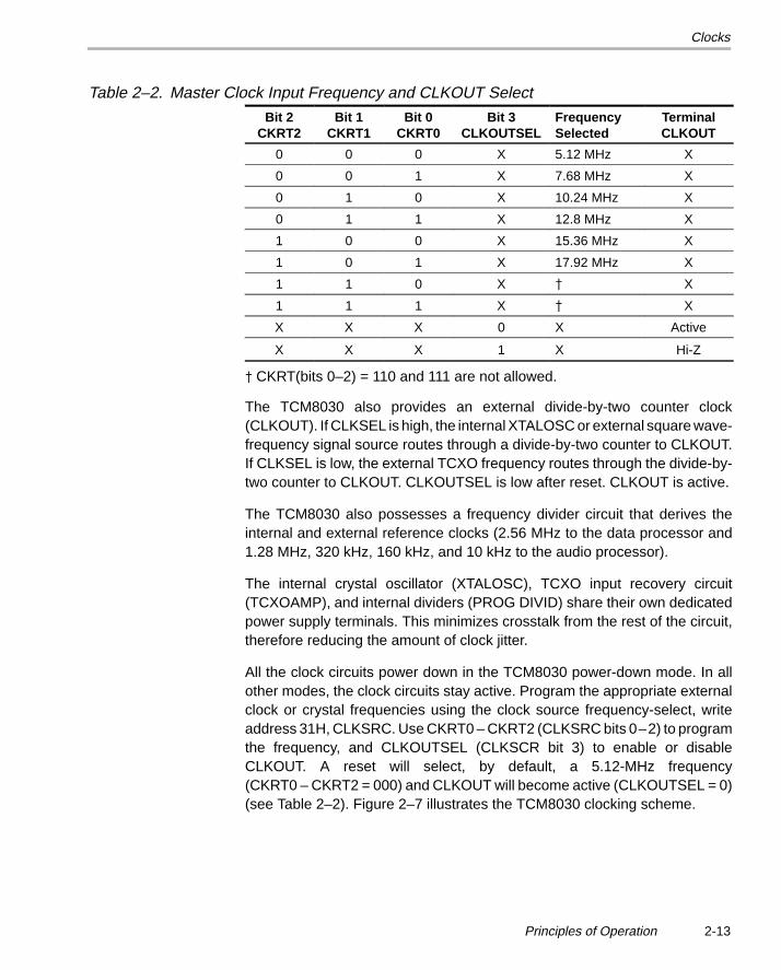
The TCM8030 has an automatic frequency control (AFC)circuit that maintainsthe accuracy of an external temperature-compensated crystal oscillator(TCXO). For the first two clock sources (XTALOSC or external square wave),the AFC circuit operates with any TCXO operating at a frequency less than20 MHz. However, for the third clock source (external TCXO), the AFCoperates with a TCXO at a frequency associated with CKRT (write address31H, bits 0–2), as shown in Table 2–2.
Clocks
2-13Principles of Operation
Table 2–2. Master Clock Input Frequency and CLKOUT Select
Bit 2CKRT2
Bit 1CKRT1
Bit 0CKRT0
Bit 3CLKOUTSEL
FrequencySelected
TerminalCLKOUT
0 0 0 X 5.12 MHz X
0 0 1 X 7.68 MHz X
0 1 0 X 10.24 MHz X
0 1 1 X 12.8 MHz X
1 0 0 X 15.36 MHz X
1 0 1 X 17.92 MHz X
1 1 0 X X
1 1 1 X X
X X X 0 X Active
X X X 1 X Hi-Z
CKRT(bits 0–2) = 110 and 111 are not allowed.
The TCM8030 also provides an external divide-by-two counter clock(CLKOUT). If CLKSEL is high, the internal XTALOSC or external square wave-frequency signal source routes through a divide-by-two counter to CLKOUT.If CLKSEL is low, the external TCXO frequency routes through the divide-by-two counter to CLKOUT. CLKOUTSEL is low after reset. CLKOUT is active.
The TCM8030 also possesses a frequency divider circuit that derives theinternal and external reference clocks (2.56 MHz to the data processor and1.28 MHz, 320 kHz, 160 kHz, and 10 kHz to the audio processor).
The internal crystal oscillator (XTALOSC), TCXO input recovery circuit(TCXOAMP), and internal dividers (PROG DIVID) share their own dedicatedpower supply terminals. This minimizes crosstalk from the rest of the circuit,therefore reducing the amount of clock jitter.
All the clock circuits power down in the TCM8030 power-down mode. In allother modes, the clock circuits stay active. Program the appropriate externalclock or crystal frequencies using the clock source frequency-select, writeaddress 31H, CLKSRC. Use CKRT0 – CKRT2 (CLKSRC bits 0–2) to programthe frequency, and CLKOUTSEL (CLKSCR bit 3) to enable or disableCLKOUT. A reset will select, by default, a 5.12-MHz frequency(CKRT0 – CKRT2 = 000) and CLKOUT will become active (CLKOUTSEL = 0)(see Table 2–2). Figure 2–7 illustrates the TCM8030 clocking scheme.
Clocks
2-14
Figure 2–7. Clocking Scheme Functional Block Diagram
AFCCONTROL
÷ 2
XTALOSC
ProgrammableDivider
CKRT0
CKRT1
CKRT2
CLKOUTSELEnZ
All Circuits
FixedDivider
IFAMP
TXCOAMP
IF
TCXO
RESETCLKSEL
CLKOUT
XOUTXIN
TCXOVDD
TCXOVSS
PWDTCXOPWDXTAL
PWDFIL
Internal Clocks
2.56 MHz
1.28 MHz
320 kHz
160 kHz
10 kHz
InternalClocks
TCK
IFAMPEN
External Clockor Crystal
Power Modes
2-15Principles of Operation
2.7 Power Modes
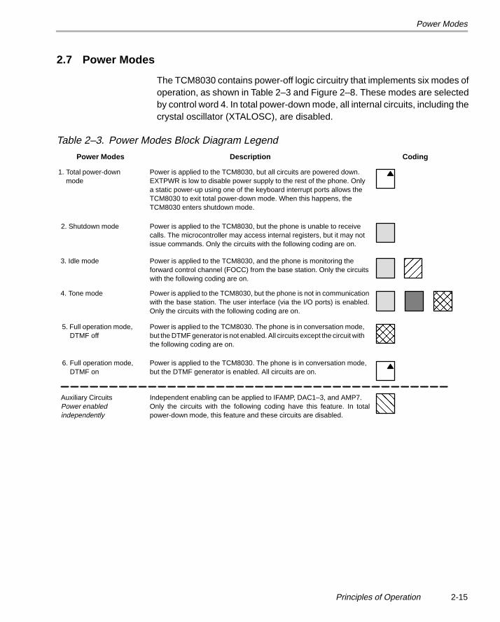
The TCM8030 contains power-off logic circuitry that implements six modes ofoperation, as shown in Table 2–3 and Figure 2–8. These modes are selectedby control word 4. In total power-down mode, all internal circuits, including thecrystal oscillator (XTALOSC), are disabled.
Table 2–3. Power Modes Block Diagram Legend
1. Total power-down mode
Power is applied to the TCM8030, but all circuits are powered down.EXTPWR is low to disable power supply to the rest of the phone. Onlya static power-up using one of the keyboard interrupt ports allows theTCM8030 to exit total power-down mode. When this happens, theTCM8030 enters shutdown mode.
2. Shutdown mode Power is applied to the TCM8030, but the phone is unable to receivecalls. The microcontroller may access internal registers, but it may notissue commands. Only the circuits with the following coding are on.
3. Idle mode Power is applied to the TCM8030, and the phone is monitoring theforward control channel (FOCC) from the base station. Only the circuitswith the following coding are on.
ÎÎÎÎ
4. Tone mode Power is applied to the TCM8030, but the phone is not in communicationwith the base station. The user interface (via the I/O ports) is enabled.Only the circuits with the following coding are on.
ÌÌÌÌÌÌ
5. Full operation mode, DTMF off
Power is applied to the TCM8030. The phone is in conversation mode,but the DTMF generator is not enabled. All circuits except the circuit withthe following coding are on.
ÌÌÌÌÌÌ
6. Full operation mode, DTMF on
Power is applied to the TCM8030. The phone is in conversation mode,but the DTMF generator is enabled. All circuits are on.
Auxiliary CircuitsPower enabledindependently
Independent enabling can be applied to IFAMP, DAC1–3, and AMP7.Only the circuits with the following coding have this feature. In totalpower-down mode, this feature and these circuits are disabled.
ÏÏÏÏÏÏ
Power Modes Description Coding
Power Modes
2-16
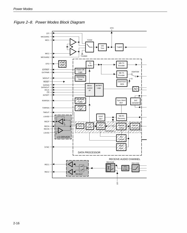
Figure 2–8. Power Modes Block Diagram
ÎÎÎÎÎÎÎÎÎÎÎÎÎÎÎÎÎÎÎÎÎÎÎÎÎÎÎÎÎÎÎÎÎÎÎÎÎÎÎÎÎÎÎÎÎÎÎÎÎÎÎÎ
ÎÎÎÎ
RXBuffer
ÎÎÎÎ
ÎÎÎÎÎÎÎÎÎÎÎÎ
Σ
Power-OffLogic
ÎÎÎÎÎÎ
V/DTrim
TXBPF
WB-TXEncoder
NB-TXEncoder
DSAT/DSTGEN
DSATSW
TXBuffer
Micro-control
I/F
INTRPTLogic ÏÏ
ÏÏ
WatchdogTimer
LS DRIVER
ÎÎÎÎ
DSATDET
ÎÎÎÎ
MajorityVoting
NB-RXRecovery
Sync WordDET
ÎÎÎÎÎÎ
WB-RXRecovery
SATGEN/DET
ÎÎÎÎ
REC1SW
VOLCTRL
RECSUM
DTI
ST
I
STO
MICGAIN1
MIC1
MIC2
MICGAIN2
DTO
EXTRST
EXTPWR
ÌÌÌÌ
WDOUT
RESET
DATAINDATAOUT
DCLKCS
INTRPT
RXRFEN
TXRFEN
TMOUT
LSVDD
RECP
RECN
LSVSS
RECIN
SYNC
REC1
REC2
TXSW
RECEIVE AUDIO CHANNEL
DATA PROCESSOR
TXVMID
DTMFGEN
AFC
RECBUF
ÎÎÎÎ
Timer
RXControl
WordSync
Idle-ModeLogic
ArbitratLogic
WB/NBSW–c
BCHDecoder
Power Modes
2-17Principles of Operation
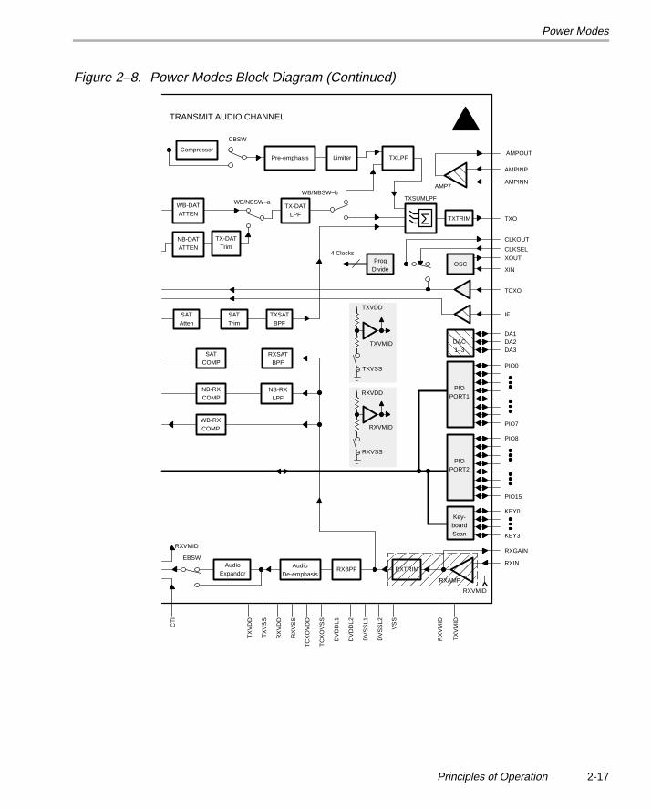
Figure 2–8. Power Modes Block Diagram (Continued)
ÎÎÎÎÎÎÎÎÎÎ
Compressor
CBSW
Pre-emphasis Limiter TXLPF
ΣTX-DAT
LPF
WB/NBSW–aWB-DATATTEN
TX-DATTrim
NB-DATATTEN
SATAtten
SATTrim
TXSATBPF
RXSATBPF
SATCOMP
NB-RXLPF
NB-RXCOMP
WB-RXCOMP
TXVMID
RXVMID
TXTRIM
ÏÏÏÏ
ÏÏÏÏTXSUMLPF
ÏÏÏÏ
DAC1–3
AMP7
4 Clocks
RXAMP
ÎÎÎÎ
RXTRIMRXBPFAudio
Expandor
EBSW
AMPOUT
AMPINP
AMPINN
TXO
CLKOUT
CLKSELXOUT
XIN
TCXO
IF
DA1DA2DA3
PIO0
PIO7
PIO8
PIO15
KEY0
KEY3
RXGAIN
RXIN
TX
VM
ID
RX
VM
ID
VS
S
DV
SS
L2
DV
SS
L1
DV
DD
L2
DV
DD
L1
TC
XO
VS
S
TC
XO
VD
D
RX
VS
S
RX
VD
D
TX
VS
S
TX
VD
D
CT
I
WB/NBSW–b
AudioDe-emphasis
TRANSMIT AUDIO CHANNEL
RXVMID
RXVMID
TXVDD
TXVSS
RXVDD
RXVSS
ProgDivide
OSC
PIOPORT1
PIOPORT2
Key-boardScan
Power Modes
2-18
2.7.1 Total Power-Down Mode
In this mode, power is still applied to the TCM8030, but the device is in totalpower-down mode. All circuits, including CLOCK, bias circuits, PIOs, and thewatchdog timer, power down. The TCM8030 stops so it draws minimalleakage current, as illustrated in Figure 2–8. The EXTPWR output terminal islow to disable the power supply to the rest of the telephone (including theMCU). The EXTRST terminal is also low, and the TCM8030 microcontrollerinterface is disabled.
The TCM8030 is the only device in the telephone with its power supply enabledin total power-down mode. Static power-up logic, implemented using one ofthe keyboard interrupt ports, waits for the power-on key to be pressed. Afterthe key is pressed, the TCM8030 exits the total power-down mode, reactivatesthe oscillator, enables the regulators to the rest of the telephone (using theEXTPWR enable signal), and holds the EXTRST terminal low for 0.1 to 0.2second, to allow the rest of the telephone to go to power-up reset mode whenthe system is stable.
The TCM8030 goes into total power-down mode by writing to control word 4,(write address 03H, C4 bits 4–0). You must toggle both control word 4 (C4)bits 1–0, with this write transaction. The security bit, C4 bit 1, reduces theprobability that the total power-down mode is entered erroneously, forexample, by RFI (radio frequency interference).
The independent analog circuits IFAMP, AMP7, and DAC1–3 also powerdown in total power-down mode, independent of the status of their own power-down control bits in register AUXPE (write address 30H).
The cellular telephone uses the total power-down mode from the firstconnection of the battery as follows:
1) The telephone receives power for the first time when the battery isconnected. Only TCM8030 initially connects to its power supply, poweringup in shutdown mode. In this mode, CLKSEL sets the TCM8030 masterclock source (see Section 2.6, Clocks), and it immediately sets EXTPWRhigh.
2) The power-up RESET input to the TCM8030 is held low during theoperation of the external power-on-reset (RC) circuit. This also holdsEXTRST at low.
3) When the external power-on reset mode finishes, EXTRST transitions tohigh, the TCM8030 microcontroller interface enables, and the MCU startsits boot routine. Because the TCM8030 INTRPT terminal is not set to one,the MCU knows that it was reset by a battery connect power up. (In this
Power Modes
2-19Principles of Operation
situation the telephone should appear to be off until the power-on key ispressed). The MCU then writes to the TCM8030 to:
Enable a keypad interrupt on the appropriate KEY pin. This requiresfour write transactions to TCM8030 registers:
PI3INT (write address 1CH) to enable the pin interrupt
PI3PULL (write address 1BH) to enable or disable the pullup asrequired
PIOC3 (write address 19H) to set direction as input
IE2 (write address 06H) to enable interrupts from the PIO3,keypad port
Set the C4 bits 4–0 to 02H to enter total power-down mode.
The MCU must first enable the keypad port terminal connected to thepower-on key before entering total power-down mode. If the MCU doesnot, only a RESET to the TCM8030 will re-enable it.
4) At this point the clock stops, EXTPWR transitions to low, EXTRSTtransitions to low, and the MCU and other parts of the system power off,waiting for the power-on key to be pressed.
5) When you press the power-on key, it is sensed on one of the KEY inputs.Asynchronous logic, which does not need the clock, reads the power-onkey, forces TCM8030 back into shutdown mode, and turns EXTPWR backon. The TCM8030 event register also records the fact that a keypadinterrupt was received.
6) EXTPWR transitions to high and powers up the microcontroller, and aftera timed interval of between 0.1 and 0.2 second, including the XTALOSCwarm-up time, TCM8030 releases EXTRST, allowing the rest of thesystem to power up and reset when the system is stable. The MCU thenexecutes its boot routine.
7) At this time, the INTRPT terminal from the TCM8030 is in active mode, andthe microcontroller checks the TCM8030 event register and determinesit was awakened by a keypad event, such as a pressed power-on key.When the MCU is awakened, the microcontroller starts to initialize theentire system, as appropriate.
2.7.2 Shutdown Mode
The microcontroller interface, clock, bias circuits, watchdog timer blocks, andall three PIOs remain operational in the shutdown mode, as illustrated in
Power Modes
2-20
Figure 2–8. The shutdown mode can be used when the telephone is switchedon but cannot receive calls, for example, while the battery is recharging. Themicrocontroller interface may access all internal registers during shutdownmode, but may not issue commands (addresses 08H to 0EH).
2.7.3 Idle Mode
In addition to the circuits that are operational in shutdown mode, the widebandreceive data path is enabled, as illustrated in Figure 2–8. This corresponds tothe telephone being in idle mode, on a forward-control channel (FOCC). Twosubmodes also activate within the idle mode to further minimize powerconsumption in the telephone. First, the MCU idle submode (see theTCM8030 Analog Baseband Data Manual description for register E2 in readaddress map – read address 06H) enables the MCU to go to sleep when itdoes not receive any new messages, and the RXRF idle submode (see theTCM8030 Analog Baseband Data Manual description for register RXRFTIMin write address map – write address 20H) powers down the RF receiver whenit is not needed.
2.7.4 Tone Mode
In addition to the circuits in shutdown mode, the DTMF generator and thesection of the RX audio path that follows the call tone input (CTI) power up intone mode, as illustrated in Figure 2–8. This mode is used when the telephonepowers up, and when the user interface, such as the keypad and usermemories, is enabled but the telephone does not communicate with the basestation.
2.7.5 Full Operation Mode, DTMF TX Off
This mode corresponds to a telephone conversation in progress. All circuitsare on, except the DTMF generator, as illustrated in Figure 2–8.
2.7.6 Full Operation Mode, DTMF TX On
This mode is enabled so that a DTMF tone can be transmitted during atelephone conversation. All circuits are on, as illustrated in Figure 2–8.
2.7.7 Independent Circuits
The IFAMP, DAC1–3, and AMP7 blocks can be individually powered down asdescribed in the AUXPE register (write address 30H). These bits areoverridden, and all circuits power down in total power-down mode, asillustrated in Figure 2–8.
Circuit Definitions
2-21Principles of Operation
2.8 Circuit Definitions
Within the TCM8030, certain circuits control specific analog basebandprocessor operations. Below is a list of these circuits and a description of theirfunction.
2.8.1 Transmit Path Audio Processing Functions
The TCM8030 audio transmit path is composed of the following circuits, asshown in Figure 2–2. A brief functional description is given for each circuit.
MIC1 and MIC2 amplifier
A pair of single-ended microphone amplifiers accept two input signals (MIC1and MIC2). Gains for MIC1 and MIC2 are set using external resistors. Outputfrom each amplifier is fed back through terminals MICGAIN1 and MICGAIN2.
TXSW
The transmit switch (TXSW) selects one of four transmit audio sources. Itselects either the voice signal from MICAMP1 or MICAMP2; the input pin DTI,which connects externally to the DTMF generator; or connects to TXVMID tomute the transmit path.
V/D Trim
The voice or DTMF trim (V/D TRIM) circuit uses an antialiasing filter to processthe audio signal before it is applied to the transmit band-pass filter. This circuitblock also provides a means to trim the voice and DTMF signal levels.
TXBPF
The transmit band-pass filter (TXBPF) is a switched capacitor band-pass filterthat passes only the transmit audio frequencies from 300 Hz to 3 kHz.
Compressor
The compressor circuit compresses the audio signal and outputs a signal witha change of 1 dB for an input signal change of 2 dB.
CBSW
The compressor bypass switch (CBSW) permits the routing of the audio signalaround the audio compressor circuit when testing the audio channel orpassing DTMF signals.
Circuit Definitions
2-22
Pre-emphasis
As audio frequencies increase, the pre-emphasis circuit increases the signalgain at a rate of 6 dB per octave across the 300-Hz to 3-kHz audio passband.
Limiter
The limiter circuit limits the transmit signal deviation within an acceptablerange. The limiter has a set gain of +6.0 dB. The limiter also maintains asoftware programmable trim with a trim range from –10.97 dB to 7.5 dB.
TXLPF
The transmit low-pass filter (TXLPF) is a switched-capacitor filter that removesharmonics caused by the (deviation) limiter. Linear-phase design preventsovershoots. This circuit is also used in narrowband mode to filter switched-capacitor output noise from TX-DAT LPF.
TXSUMLPF
The transmit-summing and low-pass filter (TXSUMLPF) is a switched-capacitor filter that selectively sums voice, data, or SAT into the audio output.It also includes a low-pass switched-capacitor filter to reduce spurious outputemissions above 10 kHz.
TXTRIM
The transmit trim stage (TXTRIM) trims the FM deviation by transmitting eitherST or wideband data prior to its output on the TXO terminal. This stage hasa continuous second-order smoothing filter that removes noise.
2.8.2 Receive Path Audio Processing Functions
The TCM8030 audio receive path is composed of the following circuits, asshown in Figure 2–2. A brief functional description is given for each circuit.
RXAMP
The receive amplifier circuit (RXAMP) receives its input from the RXINterminal. A portion of the RXAMP output is applied, through the RXGAINterminal, to a pair of external resistors that set the stage gain. The RXAMPnoninverting input internally connects to the RXVMID reference level.
RXTRIM
The receive trim (RXTRIM) stage compensates for FM discriminatorvariations. This block also contains a switched-capacitor filter to performantialiasing.
Circuit Definitions
2-23Principles of Operation
RXBPF
The receive band-pass filter (RXBPF) is a switched-capacitor filter with a pass-band from 300 Hz to 3 kHz.
DE-EMPHASIS
As audio frequencies increase, the de-emphasis circuit decreases the signalgain at a rate of 6 dB per octave across the 300-Hz to 3-kHz audio pass-band.
EXPANDOR
The audio expandor circuit expands the audio signal and outputs the signalwith a change of 2 dB for an input signal change of 1 dB.
EBSW
The expandor bypass switch (EBSW) permits the routing of the received audiosignal around the expandor during testing.
REC1SW
The receive 1 switch (REC1SW) selects one of three receive sources.REC1SW selects either the output from the expandor circuit (expanded orbypassed), the call tone (CTI) input, or selects and connects REC1SW toRXVMID to mute the receive path.
VOL CTRL
The volume control (VOL CTRL) circuit can be programmed to provide anominal gain of –20 dB to 17.5 dB for the outputs REC1 and REC2.
RECSUM
The receiver summing circuit and switch (RECSUM) provide the means foradding sidetone (STI) input into the receive audio path.
RECBUF
The receiver buffer (RECBUF) switches or mutes two output buffersindependently, or it connects these buffers in differential mode so that a piezo-speaker can be connected to REC1 and REC2 terminals. Independent controlof the two audio outputs allows one to be used for external hands-freeoperation.
LS DRIVER
The loudspeaker driver (LS DRIVER) circuit is a selectable differential orsingle-ended output earpiece amplifier. It drives a 32 Ω dynamic earpiece (ora piezoearpiece).
Circuit Definitions
2-24
2.8.3 Transmit Path Data Processing Functions
The TCM8030 data processing functions associated with the transmit path areperformed by the following circuits as shown in Figure 2–2. A brief functionaldescription is given for each circuit.
TX BUFFER
The transmit buffer (TX BUFFER) buffers both narrowband and wideband datathat is loaded from the five transmit-data word registers (TXD0 – TXD4, writeaddresses 10H–14H).
WB-TX ENCODER
The wideband transmit data encoder circuit (WB-TX ENCODER) receives thedata from the transmit buffer and performs all the necessary operations forboth the reverse control channel (RECC) and reverse voice channel (RVC)data transmission. It calculates and adds BCH parity bits to the data, along withword sync and dotting. The data is repeated as specified for analog cellular.The wideband signaling tone (ST) is generated when required.
NB-TX ENCODER
The narrowband transmit data encoder circuit (NB-TX ENCODER) calculatesthe BCH encoding parity bits from the data in the transmit buffer and adds the30-bit synch word to synchronize the transmission of RVC data to the DSAT.
DSATSW
The digital supervisory audio tone switch (DSATSW) selects either narrow-band data or the output from the DSAT/DST GEN stage for application to theNB-DAT ATTEN stage. The fifth and sixth bits of the operational control wordC1 (write address 00H) control the operation of the DSATSW. When bits 5 and6 are set to zero, the switch connects to the NB-TX encoder input.
WS/NBSW-a, -b, and -c
The wideband and narrowband switches (WB/NBSW -a through -c), groupedtogether, select either narrowband or wideband transmission operation. Theswitch position is controlled by the value in bit one of the operational controlword C1 (write address 00H).
DSAT/DST GEN
The digital supervisory audio tone/digital signaling tone generator (DSAT/DSTGEN) circuit generates the narrowband DSAT and DST signals.
Circuit Definitions
2-25Principles of Operation
NB-DAT ATTEN and WB-DAT ATTEN
These two circuits are fixed narrowband and wideband data attenuators (NB-DAT ATTEN AND WB-DAT ATTEN) that set a fixed attenuation to provide thecorrect data signal levels.
TX-DAT TRIM
The transmit data trim circuit (TX-DAT TRIM) trims the DSAT, DST, andnarrowband data levels.
TX-DAT LPF
The transmit data low-pass filter circuit (TX-DAT LPF) provides low-passswitched-capacitor filtering of the DSAT and DST. It also transmits narrowbandand wideband data to minimize output harmonics and correct narrowbandtransmitted data eye patterns.
2.8.4 Receive Path Data Processing Functions
The TCM8030 data processing functions associated with the receive path areperformed by the following circuits as shown in Figure 2–2. A brief functionaldescription is given for each circuit.
WB-RX COMP
This wideband receive comparator circuit (WB-RX COMP) features built-inhysteresis to reject noise.
WB-RX RECOVERY
This circuit performs the wideband data recovery function (WB-RXRECOVERY), including dotting.
WORD SYNC
This circuit performs frame synchronization (WORD SYNC) recovery for thewideband data channel.
NB-RX LPF
The narrowband receive data and low-pass filter circuit (NB-RX LPF) containsa low-pass switched-capacitor filter for filtering DSAT and audio signals. Thiscircuit also includes a decimating antialiasing stage at the input.
NB-RX COMP
The narrowband receive and DSAT comparator circuit (NB-RX COMP)features built-in hysteresis to reject noise.
Circuit Definitions
2-26
NB-RX RECOVERY
The narrowband data and DSAT recovery circuit (NB-RX RECOVERY)recovers the narrow-band data and DSAT components for application to theBCH decoder circuit.
SYNC WORD DET
The sync word detect circuit (SYNC WORD DET) detects the narrowband datasync word.
DSAT DET
The digital supervisory audio tone detector circuit (DSAT DET) monitors thenarrowband receive recovery data for the DSAT signal.
Majority voting
In wideband mode, each of the 40 receive data bits is majority voted. Thenumber of repeats is read using the microcontroller interface.
BCH decoder
The wideband and narrowband BCH decoder stage can correct up to twoerrors in the received signal and give a 4-bit error correction status report.
RX BUFFER
The receive buffer (RX BUFFER) stage provides a buffer for both widebandand narrowband received data.
RX CONTROL
The receive control (RX CONTROL) functional block controls the wideband/narrowband receive data recovery and decoding stages. It splits the time-multiplexed busy/idle bits, chooses word A or B, and starts the majority voteand error correction processes, when required.
ARBITRAT LOGIC
The arbitration logic circuit (ARBITRAT LOGIC) arbitrates wideband databusy/idle bits majority voting and outputs the results to the TXRFEN terminal.
IDLE MODE LOGIC
The idle-mode logic circuit senses the microcontroller unit (MCU) idle modeand receive RF (RXRF) idle-mode functions, and applies an enable signal tothe output terminal RXRFEN to control the internal power mode.
2.8.5 Transmit Path SAT Processing Functions
The TCM8030 supervisory audio tone (SAT) transmit-path processingfunctions are performed by the following circuits, as shown in Figure 2–2. Abrief functional description is given for each circuit.
Circuit Definitions
2-27Principles of Operation
SAT GEN/DET
The supervisory audio tone generator and detector (SAT GEN/DET) circuit isprimarily a transponding digital phased-locked loop (PLL) circuit. It is used inwideband mode only. The circuit is an enhanced design that improves SATsensitivity. SAT outputs can also be programmed without a SAT input tofacilitate phone testing.
SAT ATTEN
The supervisory audio tone attenuator (SAT ATTEN) circuit is a fixedattenuator used to set the correct TX SAT signal level.
SAT TRIM
The supervisory audio tone trim (SAT TRIM) circuit sets the wide-band SATlevel trim. Output from this circuit is applied to the TXSAT BPF antialiasingfilter.
TXSAT BPF
The transmit band-pass filter (TXSAT BPF) circuit is a switched-capacitorband-pass filter that performs antialiasing.
2.8.6 Receive Path SAT Processing Functions
The TCM8030 supervisory audio tone (SAT) receive-path processingfunctions are performed by the following circuits, as shown in Figure 2–2. Abrief functional description is given for each circuit.
RXSAT BPF
The receive band-pass filter (RXSAT BPF) circuit for the supervisory audiotone is a switched-capacitor band-pass filter.
SAT COMP
The supervisory audio tone comparator (SAT COMP) circuit slices thereceived SAT signal before sending it to the SAT GEN/DET circuit. This circuitalso contains built-in hysteresis to aid in noise rejection.
Miscellaneous Functions
2-28
2.9 Miscellaneous Functions
The TCM8030 contains several circuits that perform specific functions aspreviously shown in Figure 2–2. A brief functional description is given for eachcircuit.
Power-Off Logic
This function implements total power-down mode logic. In this mode, allinternal circuits, including the XTALOSC, are disabled. The TCM8030 is theonly device in the phone with its power supply enabled in this mode. Staticpower- up logic, implemented via one of the keyboard interrupt ports, waits fora pressed power-on key. Then TCM8030 exits total power-down mode,reactivates the oscillator, enables the regulators to the rest of the phone viaEXTPWR, and holds EXTRST low for 0.1 to 0.2 second, to allow the rest of thephone to power up cleanly.
TXVMID and RXVMID
The TXVMID and RXVMID functional blocks are separate transmit andreceive analog-reference voltage generators. The circuits contain resistivedividers fed from analog voltage supplies. The outputs are buffered and thendecoupled externally, to provide accurate, quiet, mid-rail reference to internalaudio circuits.
AFC
The AFC (automatic frequency control) circuit receives one input from anexternal TCXO (temperature-compensated crystal oscillator) and anotherinput from the receiver IF (intermediate frequency) stage. The counters in thisblock then process the inputs and provide a count that can be read using themicrocontroller interface.
DAC 1–3
DACs 1–3 are each 8-bit linear digital-to-analog converters.
AMP7
AMP7 is an uncommitted operational amplifier.
DTMF GEN
The dual-tone multifrequency generator (DTMF GEN) circuit generates thetones for push-button dialing and provides the user-alert tone.
Timer
The timer circuit is a programmable 8-bit counter. The timer can either countdown once or cycle continuously. When the counter reaches zero, the outputchanges state.
Miscellaneous Functions
2-29Principles of Operation
Watchdog timer
The watchdog timer circuit starts by writing to a location in the microcontrollerinterface. If the location is not written to again within the time-out period, thewatchdog timer times out and the output changes state. This change in outputresets the telephone microcontroller.
PIO Port 1 and PIO Port 2
PIO Port 1 and PIO Port 2 are two 8-bit wide programmable ports. Each lineof each port can be individually programmed as either an input or an output.
Keyboard scan
The keyboard scan port is a 4-bit port that accepts inputs from a keyboard andgenerates interrupts to the microcontroller. The port can also be reconfiguredas a general purpose I/O (input/output) port. One I/O terminal connected to thetelephone ON/OFF key supplies a wake-up signal that terminates the totalpower-down mode.
MICRO CONTRL I/F and INTRPT LOGIC
All wideband and narrowband data communications are transmitted to andreceived from the telephone microcontroller using the microcontrollerinterface (MICRO CONTRL I/F) circuitry. Internal data, command, andinterrupt registers are programmed using the write operation. Other internaldata, status, and interrupt registers are monitored using read operations.
3-1
Receive Processing
This chapter describes the receive processing procedure for the forwardcontrol channel (FOCC) and the forward voice channel (FVC). In addition toa description of each mode, it includes examples that describe and illustratethe processing methodology.
Topic Page
3.1 Receive Processing Overview 3-2. . . . . . . . . . . . . . . . . . . . . . . . . . . . . . . . . .
3.2 Forward Control Channel (FOCC) Receive Processing 3-4. . . . . . . . . . .
3.3 Forward Voice Channel (FVC) Receive Processing 3-8. . . . . . . . . . . . . . .
Chapter 3
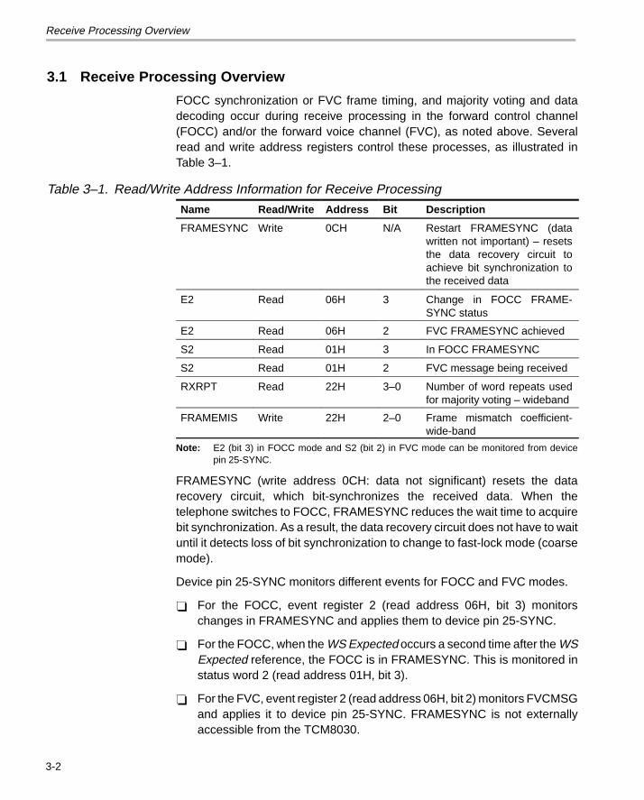
Receive Processing Overview
3-2
3.1 Receive Processing Overview
FOCC synchronization or FVC frame timing, and majority voting and datadecoding occur during receive processing in the forward control channel(FOCC) and/or the forward voice channel (FVC), as noted above. Severalread and write address registers control these processes, as illustrated inTable 3–1.
Table 3–1. Read/Write Address Information for Receive Processing
Name Read/Write Address Bit Description
FRAMESYNC Write 0CH N/A Restart FRAMESYNC (datawritten not important) – resetsthe data recovery circuit toachieve bit synchronization tothe received data
E2 Read 06H 3 Change in FOCC FRAME-SYNC status
E2 Read 06H 2 FVC FRAMESYNC achieved
S2 Read 01H 3 In FOCC FRAMESYNC
S2 Read 01H 2 FVC message being received
RXRPT Read 22H 3–0 Number of word repeats usedfor majority voting – wideband
FRAMEMIS Write 22H 2–0 Frame mismatch coefficient-wide-band
Note: E2 (bit 3) in FOCC mode and S2 (bit 2) in FVC mode can be monitored from devicepin 25-SYNC.
FRAMESYNC (write address 0CH: data not significant) resets the datarecovery circuit, which bit-synchronizes the received data. When thetelephone switches to FOCC, FRAMESYNC reduces the wait time to acquirebit synchronization. As a result, the data recovery circuit does not have to waituntil it detects loss of bit synchronization to change to fast-lock mode (coarsemode).
Device pin 25-SYNC monitors different events for FOCC and FVC modes.
For the FOCC, event register 2 (read address 06H, bit 3) monitorschanges in FRAMESYNC and applies them to device pin 25-SYNC.
For the FOCC, when the WS Expected occurs a second time after the WSExpected reference, the FOCC is in FRAMESYNC. This is monitored instatus word 2 (read address 01H, bit 3).
For the FVC, event register 2 (read address 06H, bit 2) monitors FVCMSGand applies it to device pin 25-SYNC. FRAMESYNC is not externallyaccessible from the TCM8030.
Receive Processing Overview
3-3Receive Processing
For the FVC, after the FVC dotting pattern is detected, when the first WSExpected occurs, the FVC message is being received. This is monitoredin status word 2 (read address 01H, bit 2).
RXRPT (read address 22H, bits 3–0) reports the number of repeats thatwere actually used during bit-wise majority voting.
Along with SYNC monitoring, there is also a FRAMEMIS write register thatcontrols the number of allowable, missed word syncs before FRAMESYNCtransitions from high back to low. The TCM8030 has a default value ofFRAMEMIS = 5. Therefore, if five word synchronizations are missed, theFRAMESYNC is lost, and the resynchronization process reoccurs.
Note:
The default value for FRAMEMIS (FRAMEMIS = 5) is used as the referencein the following FOCC and FVC receive-processing examples. Also, E2(bit 3) and S2 (bit 2) can be monitored from device pin 25-SYNC.
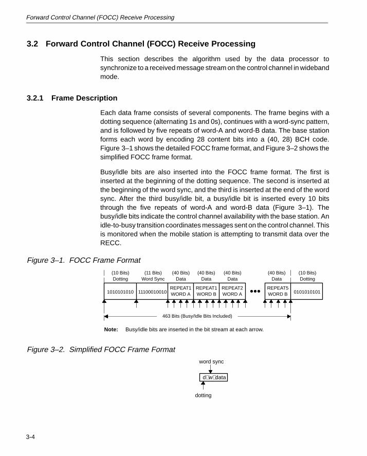
Forward Control Channel (FOCC) Receive Processing
3-4
3.2 Forward Control Channel (FOCC) Receive Processing
This section describes the algorithm used by the data processor tosynchronize to a received message stream on the control channel in widebandmode.
3.2.1 Frame Description
Each data frame consists of several components. The frame begins with adotting sequence (alternating 1s and 0s), continues with a word-sync pattern,and is followed by five repeats of word-A and word-B data. The base stationforms each word by encoding 28 content bits into a (40, 28) BCH code.Figure 3–1 shows the detailed FOCC frame format, and Figure 3–2 shows thesimplified FOCC frame format.
Busy/idle bits are also inserted into the FOCC frame format. The first isinserted at the beginning of the dotting sequence. The second is inserted atthe beginning of the word sync, and the third is inserted at the end of the wordsync. After the third busy/idle bit, a busy/idle bit is inserted every 10 bitsthrough the five repeats of word-A and word-B data (Figure 3–1). Thebusy/idle bits indicate the control channel availability with the base station. Anidle-to-busy transition coordinates messages sent on the control channel. Thisis monitored when the mobile station is attempting to transmit data over theRECC.
Figure 3–1. FOCC Frame Format
1010101010 11100010010REPEAT1WORD A
REPEAT1WORD B
REPEAT2WORD A
REPEAT5WORD B 0101010101
463 Bits (Busy/Idle Bits Included)
(10 Bits)Dotting
(11 Bits)Word Sync
(40 Bits)Data
(40 Bits)Data
(40 Bits)Data
(40 Bits)Data
(10 Bits)Dotting
Note: Busy/idle bits are inserted in the bit stream at each arrow.
Figure 3–2. Simplified FOCC Frame Format
d w data
dotting
word sync
Forward Control Channel (FOCC) Receive Processing
3-5Receive Processing
3.2.2 Synchronization
When the data processor switches into FOCC mode, it attempts tosynchronize to the received data stream in the following manner:
1) The microcontroller places the data recovery PLL into coarse mode. Thisallows the PLL to shift by 180 degrees within five data edges. In this mode,the PLL attempts to lock onto any distinct data arriving at the AMPS/TACSdata rate.
2) The RX controller evaluates the recovered data. When the controllerrecognizes the dotting pattern, the microcontroller places the PLL into finemode where it can only shift a few degrees per cycle. FCCDOT (writeaddress 23H) sets the number of dotting bits required before recognitionoccurs. The default value for this address is 07H.
3) The RX controller recognizes a word sync. With this recognition, thecontroller sets a timer that generates a WS Expected pulse exactly oneframe later. If the next word sync arrives at the same time as WS Expected,then FOCC FRAMESYNC (status word 2: read address 01H bit 3) is raisedto indicate the achieved synchronization. For the remainder of the frame,the PLL is frozen. When the dotting at the beginning of the next frame isexpected, the PLL returns to fine mode, but only until the end of the dotting,where it freezes again.
FOCC FRAMESYNC enables evaluation of the received data. When FOCCFRAMESYNC is high, the RX controller decodes and reports on the frame dataeven if the dotting pattern or word sync is corrupted (corruption in the preambledoes not mean that the data is bad). If word syncs do not occur for a specificnumber of frames indicated from the value in FRAMEMIS, FOCCFRAMESYNC transitions to low (no data is decoded) and the synchronizationprocess, in steps 1–3 above, repeats.
3.2.3 Majority Voting
Majority voting occurs on all available data repeats in wideband mode. A 40×4register contains a summation of all repeats of the 40 bits. When the registerreceives bit n of the current repeat, load the nth slice of the register into acounter. If the received bit is 1, the counter increments. If the received bit is 0,the counter decrements. The counter can count from 0 to 7 or –7.
There are five data repeats in FOCC mode. A majority vote of three out of fivewords determines whether to eliminate the recognition of corrupted data. Allfive repeats are always loaded into the majority vote logic so there is alwaysa positive or negative number assigned to the register and never zero.
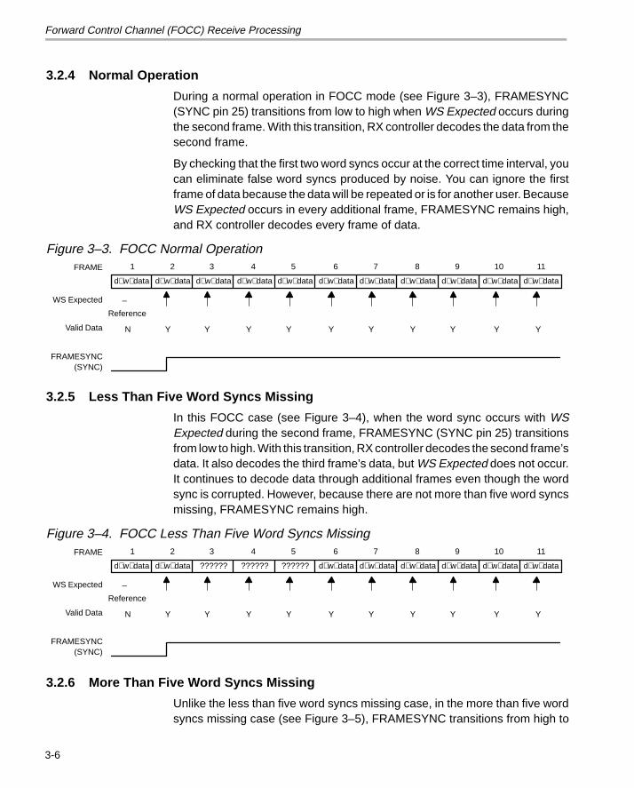
Forward Control Channel (FOCC) Receive Processing
3-6
3.2.4 Normal Operation
During a normal operation in FOCC mode (see Figure 3–3), FRAMESYNC(SYNC pin 25) transitions from low to high when WS Expected occurs duringthe second frame. With this transition, RX controller decodes the data from thesecond frame.
By checking that the first two word syncs occur at the correct time interval, youcan eliminate false word syncs produced by noise. You can ignore the firstframe of data because the data will be repeated or is for another user. BecauseWS Expected occurs in every additional frame, FRAMESYNC remains high,and RX controller decodes every frame of data.
Figure 3–3. FOCC Normal Operation
d w data d w data d w data d w data d w data d w data d w data d w data d w data d w data d w data
1 2 3 4 5 6 7 8 9 10 11
–
Reference
N Y Y Y Y Y Y Y Y Y Y
FRAME
WS Expected
Valid Data
FRAMESYNC(SYNC)
3.2.5 Less Than Five Word Syncs Missing
In this FOCC case (see Figure 3–4), when the word sync occurs with WSExpected during the second frame, FRAMESYNC (SYNC pin 25) transitionsfrom low to high. With this transition, RX controller decodes the second frame’sdata. It also decodes the third frame’s data, but WS Expected does not occur.It continues to decode data through additional frames even though the wordsync is corrupted. However, because there are not more than five word syncsmissing, FRAMESYNC remains high.
Figure 3–4. FOCC Less Than Five Word Syncs Missing
d w data d w data ?????? ?????? ?????? d w data d w data d w data d w data d w data d w data
1 2 3 4 5 6 7 8 9 10 11
–
Reference
N Y Y Y Y Y Y Y Y Y Y
FRAME
WS Expected
Valid Data
FRAMESYNC(SYNC)
3.2.6 More Than Five Word Syncs Missing
Unlike the less than five word syncs missing case, in the more than five wordsyncs missing case (see Figure 3–5), FRAMESYNC transitions from high to
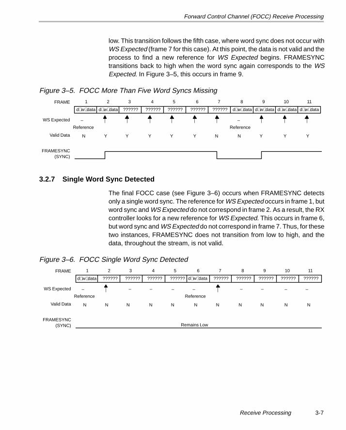
Forward Control Channel (FOCC) Receive Processing
3-7Receive Processing
low. This transition follows the fifth case, where word sync does not occur withWS Expected (frame 7 for this case). At this point, the data is not valid and theprocess to find a new reference for WS Expected begins. FRAMESYNCtransitions back to high when the word sync again corresponds to the WSExpected. In Figure 3–5, this occurs in frame 9.
Figure 3–5. FOCC More Than Five Word Syncs Missing
d w data d w data ?????? ?????? ?????? d w data d w data d w data d w data
1 2 3 4 5 6 7 8 9 10 11
–
Reference
N Y Y Y Y Y N N Y Y Y
FRAME
WS Expected
Valid Data
FRAMESYNC(SYNC)
?????? ??????
–
Reference
3.2.7 Single Word Sync Detected
The final FOCC case (see Figure 3–6) occurs when FRAMESYNC detectsonly a single word sync. The reference for WS Expected occurs in frame 1, butword sync and WS Expected do not correspond in frame 2. As a result, the RXcontroller looks for a new reference for WS Expected. This occurs in frame 6,but word sync and WS Expected do not correspond in frame 7. Thus, for thesetwo instances, FRAMESYNC does not transition from low to high, and thedata, throughout the stream, is not valid.
Figure 3–6. FOCC Single Word Sync Detected
d w data ?????? ?????? ??????
1 2 3 4 5 6 7 8 9 10 11
–
Reference
N N N N N N N N N N N
FRAME
WS Expected
Valid Data
FRAMESYNC(SYNC)
?????? ??????
–
Reference
d w data ?????? ?????? ?????? ??????
––– ––––
Remains Low
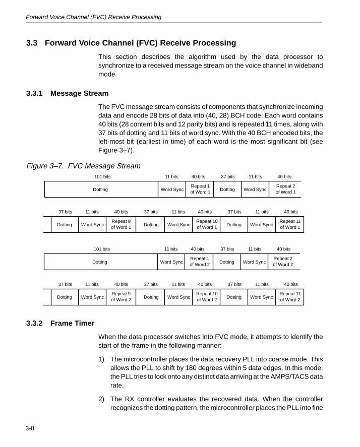
Forward Voice Channel (FVC) Receive Processing
3-8
3.3 Forward Voice Channel (FVC) Receive Processing
This section describes the algorithm used by the data processor tosynchronize to a received message stream on the voice channel in widebandmode.
3.3.1 Message Stream
The FVC message stream consists of components that synchronize incomingdata and encode 28 bits of data into (40, 28) BCH code. Each word contains40 bits (28 content bits and 12 parity bits) and is repeated 11 times, along with37 bits of dotting and 11 bits of word sync. With the 40 BCH encoded bits, theleft-most bit (earliest in time) of each word is the most significant bit (seeFigure 3–7).
Figure 3–7. FVC Message Stream
Dotting Word SyncRepeat 9of Word 1
37 bits
Repeat 10of Word 1Dotting Word Sync Dotting Word Sync
Repeat 11of Word 1
11 bits 40 bits 37 bits 11 bits 40 bits 37 bits 11 bits 40 bits
Repeat 1of Word 1Dotting Word Sync Dotting Word Sync
Repeat 2of Word 1
101 bits 11 bits 40 bits 37 bits 11 bits 40 bits
Dotting Word SyncRepeat 9of Word 2
37 bits
Repeat 10of Word 2Dotting Word Sync Dotting Word Sync
Repeat 11of Word 2
11 bits 40 bits 37 bits 11 bits 40 bits 37 bits 11 bits 40 bits
Repeat 1of Word 2Dotting Word Sync Dotting Word Sync
Repeat 2of Word 2
101 bits 11 bits 40 bits 37 bits 11 bits 40 bits
3.3.2 Frame Timer
When the data processor switches into FVC mode, it attempts to identify thestart of the frame in the following manner:
1) The microcontroller places the data recovery PLL into coarse mode. Thisallows the PLL to shift by 180 degrees within 5 data edges. In this mode,the PLL tries to lock onto any distinct data arriving at the AMPS/TACS datarate.
2) The RX controller evaluates the recovered data. When the controllerrecognizes the dotting pattern, the microcontroller places the PLL into fine
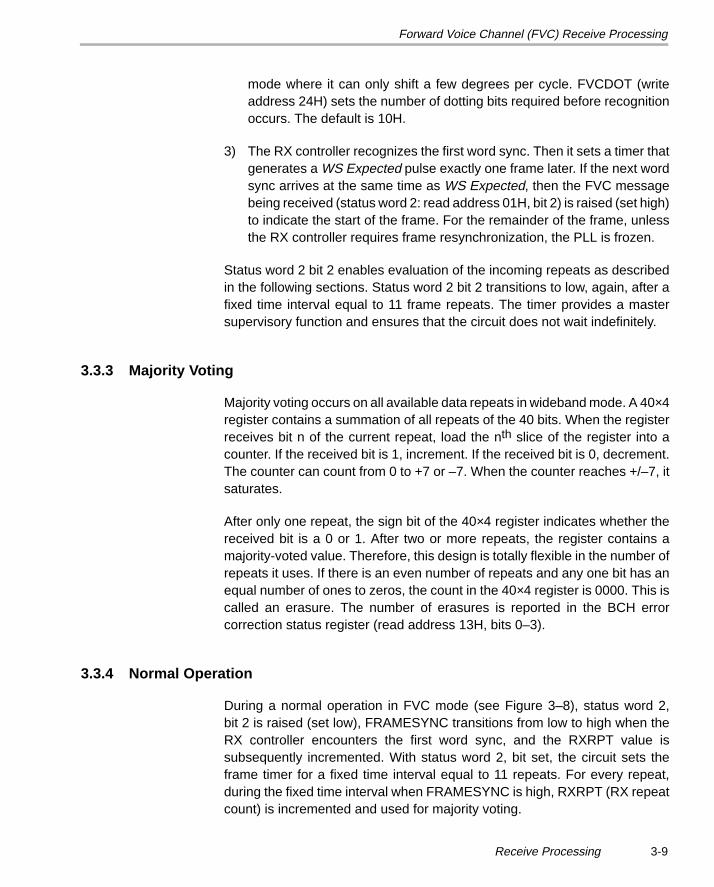
Forward Voice Channel (FVC) Receive Processing
3-9Receive Processing
mode where it can only shift a few degrees per cycle. FVCDOT (writeaddress 24H) sets the number of dotting bits required before recognitionoccurs. The default is 10H.
3) The RX controller recognizes the first word sync. Then it sets a timer thatgenerates a WS Expected pulse exactly one frame later. If the next wordsync arrives at the same time as WS Expected, then the FVC messagebeing received (status word 2: read address 01H, bit 2) is raised (set high)to indicate the start of the frame. For the remainder of the frame, unlessthe RX controller requires frame resynchronization, the PLL is frozen.
Status word 2 bit 2 enables evaluation of the incoming repeats as describedin the following sections. Status word 2 bit 2 transitions to low, again, after afixed time interval equal to 11 frame repeats. The timer provides a mastersupervisory function and ensures that the circuit does not wait indefinitely.
3.3.3 Majority Voting
Majority voting occurs on all available data repeats in wideband mode. A 40×4register contains a summation of all repeats of the 40 bits. When the registerreceives bit n of the current repeat, load the nth slice of the register into acounter. If the received bit is 1, increment. If the received bit is 0, decrement.The counter can count from 0 to +7 or –7. When the counter reaches +/–7, itsaturates.
After only one repeat, the sign bit of the 40×4 register indicates whether thereceived bit is a 0 or 1. After two or more repeats, the register contains amajority-voted value. Therefore, this design is totally flexible in the number ofrepeats it uses. If there is an even number of repeats and any one bit has anequal number of ones to zeros, the count in the 40×4 register is 0000. This iscalled an erasure. The number of erasures is reported in the BCH errorcorrection status register (read address 13H, bits 0–3).
3.3.4 Normal Operation
During a normal operation in FVC mode (see Figure 3–8), status word 2,bit 2 is raised (set low), FRAMESYNC transitions from low to high when theRX controller encounters the first word sync, and the RXRPT value issubsequently incremented. With status word 2, bit set, the circuit sets theframe timer for a fixed time interval equal to 11 repeats. For every repeat,during the fixed time interval when FRAMESYNC is high, RXRPT (RX repeatcount) is incremented and used for majority voting.
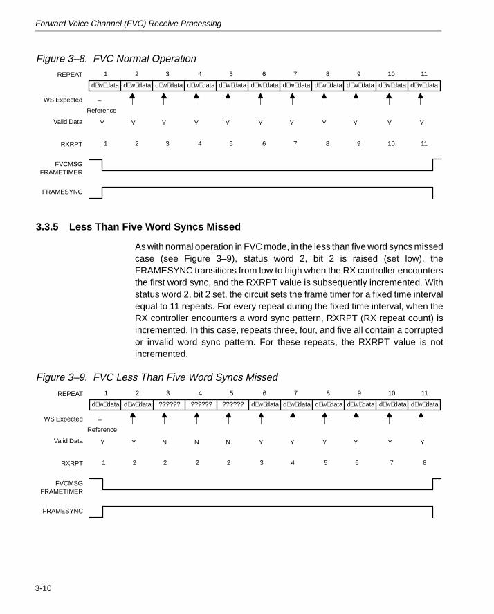
Forward Voice Channel (FVC) Receive Processing
3-10
Figure 3–8. FVC Normal Operation
d w data d w data d w data d w data d w data d w data d w data d w data d w data d w data d w data
1 2 3 4 5 6 7 8 9 10 11
–
Reference
Y Y Y Y Y Y Y Y Y Y Y
REPEAT
WS Expected
Valid Data
FRAMESYNC
1 2 3 4 5 6 7 8 9 10 11RXRPT
FVCMSGFRAMETIMER
3.3.5 Less Than Five Word Syncs Missed
As with normal operation in FVC mode, in the less than five word syncs missedcase (see Figure 3–9), status word 2, bit 2 is raised (set low), theFRAMESYNC transitions from low to high when the RX controller encountersthe first word sync, and the RXRPT value is subsequently incremented. Withstatus word 2, bit 2 set, the circuit sets the frame timer for a fixed time intervalequal to 11 repeats. For every repeat during the fixed time interval, when theRX controller encounters a word sync pattern, RXRPT (RX repeat count) isincremented. In this case, repeats three, four, and five all contain a corruptedor invalid word sync pattern. For these repeats, the RXRPT value is notincremented.
Figure 3–9. FVC Less Than Five Word Syncs Missed
d w data d w data ?????? ?????? ?????? d w data d w data d w data d w data d w data d w data
1 2 3 4 5 6 7 8 9 10 11
–
Reference
Y Y N N N Y Y Y Y Y Y
REPEAT
WS Expected
Valid Data
FRAMESYNC
1 2 2 2 2 3 4 5 6 7 8RXRPT
FVCMSGFRAMETIMER
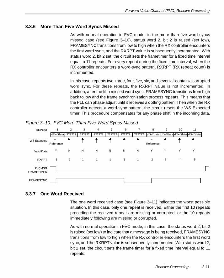
Forward Voice Channel (FVC) Receive Processing
3-11Receive Processing
3.3.6 More Than Five Word Syncs Missed
As with normal operation in FVC mode, in the more than five word syncsmissed case (see Figure 3–10), status word 2, bit 2 is raised (set low),FRAMESYNC transitions from low to high when the RX controller encountersthe first word sync, and the RXRPT value is subsequently incremented. Withstatus word 2, bit 2 set, the circuit sets the frametimer for a fixed time intervalequal to 11 repeats. For every repeat during the fixed time interval, when theRX controller encounters a word-sync pattern, RXRPT (RX repeat count) isincremented.
In this case, repeats two, three, four, five, six, and seven all contain a corruptedword sync. For these repeats, the RXRPT value is not incremented. Inaddition, after the fifth missed word sync, FRAMESYNC transitions from highback to low and the frame synchronization process repeats. This means thatthe PLL can phase-adjust until it receives a dotting pattern. Then when the RXcontroller detects a word-sync pattern, the circuit resets the WS Expectedtimer. This procedure compensates for any phase shift in the incoming data.
Figure 3–10. FVC More Than Five Word Syncs Missed
d w data ?????? ?????? ?????? d w data d w data d w data d w data
1 2 3 4 5 6 7 8 9 10 11
–
Reference
Y N N N N N N Y Y Y Y
REPEAT
WS Expected
Valid Data
FRAMESYNC
1 1 1 1 1 1 1 2 3 4 5RXRPT
FVCMSGFRAMETIMER
?????? ?????? ??????
–
Reference
3.3.7 One Word Received
The one word received case (see Figure 3–11) indicates the worst possiblesituation. In this case, only one repeat is received. Either the first 10 repeatspreceding the received repeat are missing or corrupted, or the 10 repeatsimmediately following are missing or corrupted.
As with normal operation in FVC mode, in this case, the status word 2, bit 2is raised (set low) to indicate that a message is being received, FRAMESYNCtransitions from low to high when the RX controller encounters the first wordsync, and the RXRPT value is subsequently incremented. With status word 2,bit 2 set, the circuit sets the frame timer for a fixed time interval equal to 11repeats.
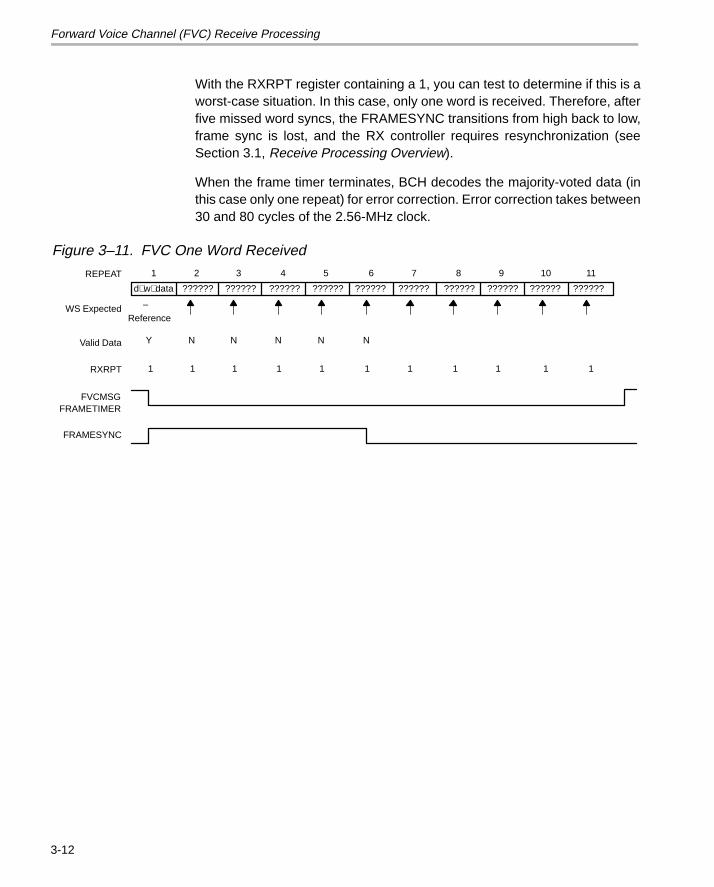
Forward Voice Channel (FVC) Receive Processing
3-12
With the RXRPT register containing a 1, you can test to determine if this is aworst-case situation. In this case, only one word is received. Therefore, afterfive missed word syncs, the FRAMESYNC transitions from high back to low,frame sync is lost, and the RX controller requires resynchronization (seeSection 3.1, Receive Processing Overview).
When the frame timer terminates, BCH decodes the majority-voted data (inthis case only one repeat) for error correction. Error correction takes between30 and 80 cycles of the 2.56-MHz clock.
Figure 3–11. FVC One Word Received
d w data ?????? ?????? ??????
1 2 3 4 5 6 7 8 9 10 11
–
Reference
Y N N N N N
REPEAT
WS Expected
Valid Data
FRAMESYNC
1 1 1 1 1 1 1 1 1 1 1RXRPT
FVCMSGFRAMETIMER
?????? ?????? ?????? ?????? ?????? ?????? ??????
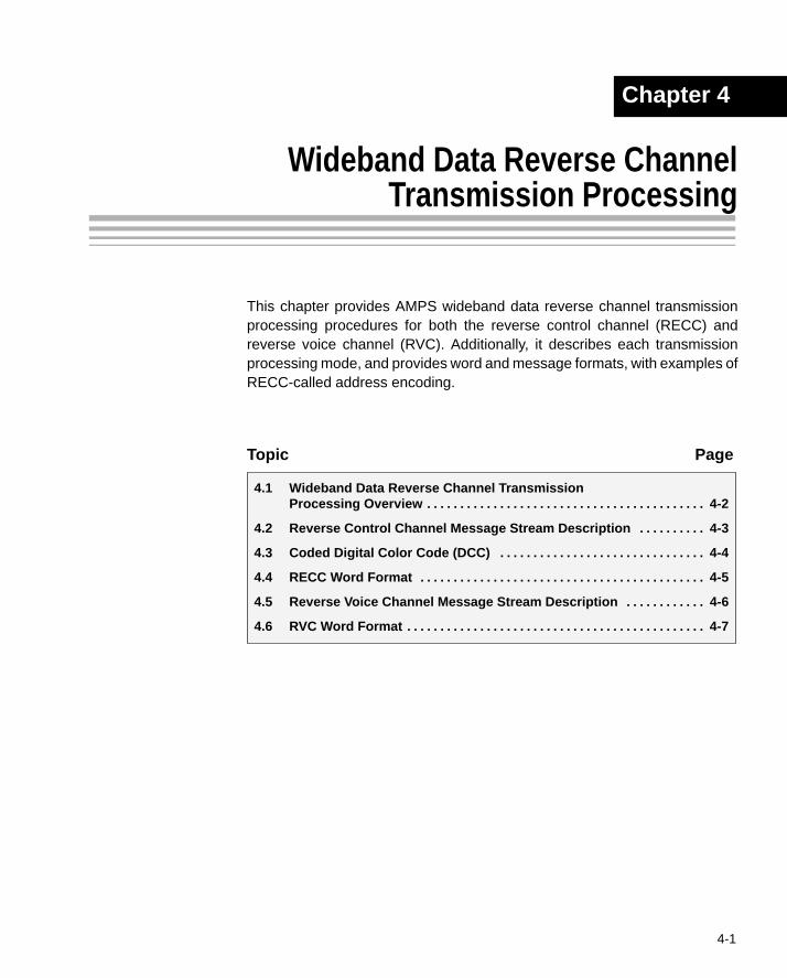
4-1
Wideband Data Reverse ChannelTransmission Processing
This chapter provides AMPS wideband data reverse channel transmissionprocessing procedures for both the reverse control channel (RECC) andreverse voice channel (RVC). Additionally, it describes each transmissionprocessing mode, and provides word and message formats, with examples ofRECC-called address encoding.
Topic Page
4.1 Wideband Data Reverse Channel Transmission Processing Overview 4-2. . . . . . . . . . . . . . . . . . . . . . . . . . . . . . . . . . . . . . . . . .
4.2 Reverse Control Channel Message Stream Description 4-3. . . . . . . . . .
4.3 Coded Digital Color Code (DCC) 4-4. . . . . . . . . . . . . . . . . . . . . . . . . . . . . . .
4.4 RECC Word Format 4-5. . . . . . . . . . . . . . . . . . . . . . . . . . . . . . . . . . . . . . . . . . .
4.5 Reverse Voice Channel Message Stream Description 4-6. . . . . . . . . . . .
4.6 RVC Word Format 4-7. . . . . . . . . . . . . . . . . . . . . . . . . . . . . . . . . . . . . . . . . . . . .
Chapter 4
Wideband Data Reverse Channel Transmission Processing Overview
4-2
4.1 Wideband Data Reverse Channel Transmission Processing Overview
Wideband transmission processing allows you to transmit responses, orders,and confirmations using the reverse control channel (RECC) and the reversevoice channel (RVC).
On the reverse control channel (RECC), a wideband data stream generatedat 10k bits/s ±1 bit/second for AMPS standard is sent from the mobile stationto the base station. The TCM8030 RECC message consists of from one toseven words for either single- or multiple-word transmissions. The messagetypes sent over the RECC are as follows:
Page response message Origination message Order confirmation message Order message
On the reverse voice channel (RVC), a wideband data stream generated at a100 bit/s Manchester rate for AMPS standard is sent from the mobile stationto the base station. The TCM8030 RVC message consists of from one to fourwords for single- or multiple-word transmissions. The message types sentover the RVC are as follows:
Order confirmation message Called-address message Unique challenge order confirmation Base station challenge order message
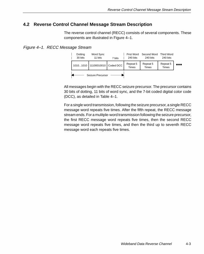
Reverse Control Channel Message Stream Description
4-3Wideband Data Reverse Channel
4.2 Reverse Control Channel Message Stream Description
The reverse control channel (RECC) consists of several components. Thesecomponents are illustrated in Figure 4–1.
Figure 4–1. RECC Message Stream
1010...1010 11100010010
Dotting30 bits
Repeat 5Times
Word Sync11 bits 7 bits
Coded DCC
First Word240 bits
Seizure Precursor
Repeat 5Times
Second Word240 bits
Repeat 5Times
Third Word240 bits
All messages begin with the RECC seizure precursor. The precursor contains30 bits of dotting, 11 bits of word sync, and the 7-bit coded digital color code(DCC), as detailed in Table 4–1.
For a single word transmission, following the seizure precursor, a single RECCmessage word repeats five times. After the fifth repeat, the RECC messagestream ends. For a mulitple-word transmission following the seizure precursor,the first RECC message word repeats five times, then the second RECCmessage word repeats five times, and then the third up to seventh RECCmessage word each repeats five times.
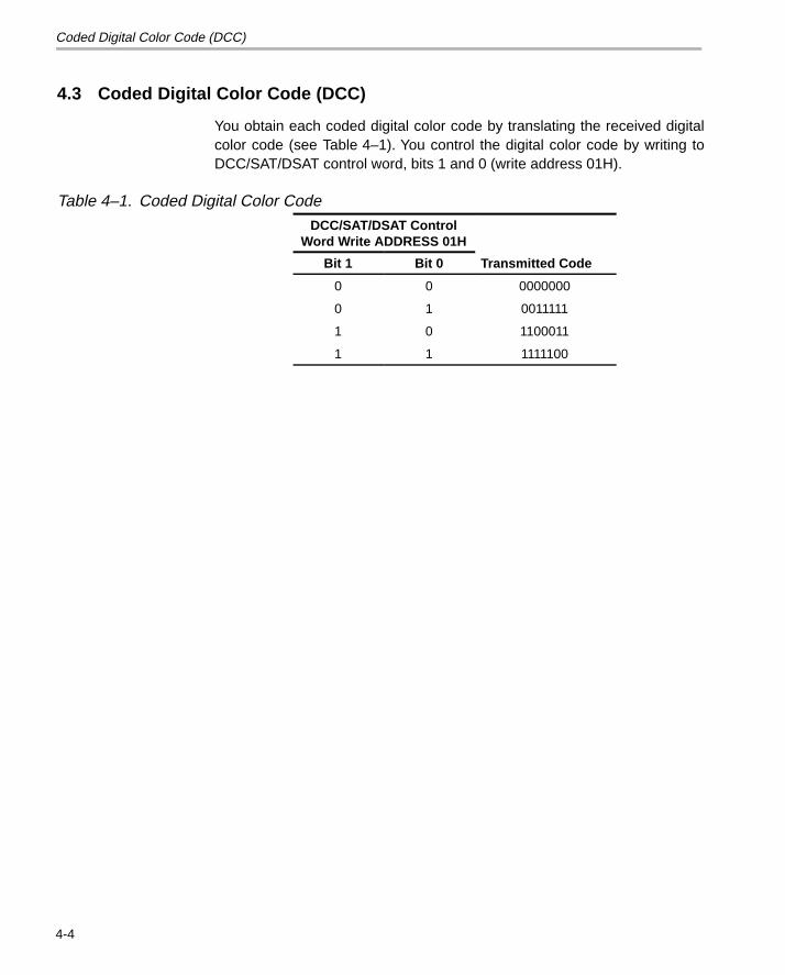
Coded Digital Color Code (DCC)
4-4
4.3 Coded Digital Color Code (DCC)
You obtain each coded digital color code by translating the received digitalcolor code (see Table 4–1). You control the digital color code by writing toDCC/SAT/DSAT control word, bits 1 and 0 (write address 01H).
Table 4–1. Coded Digital Color CodeDCC/SAT/DSAT Control
Word Write ADDRESS 01H
Bit 1 Bit 0 Transmitted Code
0 0 0000000
0 1 0011111
1 0 1100011
1 1 1111100
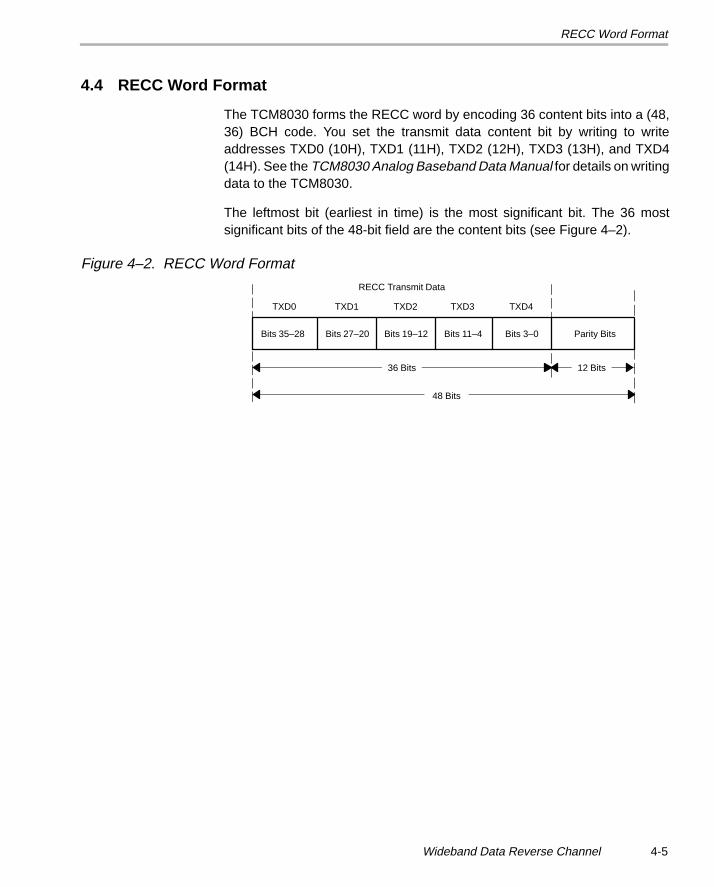
RECC Word Format
4-5Wideband Data Reverse Channel
4.4 RECC Word Format
The TCM8030 forms the RECC word by encoding 36 content bits into a (48,36) BCH code. You set the transmit data content bit by writing to writeaddresses TXD0 (10H), TXD1 (11H), TXD2 (12H), TXD3 (13H), and TXD4(14H). See the TCM8030 Analog Baseband Data Manual for details on writingdata to the TCM8030.
The leftmost bit (earliest in time) is the most significant bit. The 36 mostsignificant bits of the 48-bit field are the content bits (see Figure 4–2).
Figure 4–2. RECC Word Format
Bits 35–28
TXD0
Parity Bits
36 Bits
48 Bits
TXD1
Bits 27–20
TXD2
Bits 19–12
TXD3
Bits 11–4
TXD4
Bits 3–0
12 Bits
RECC Transmit Data
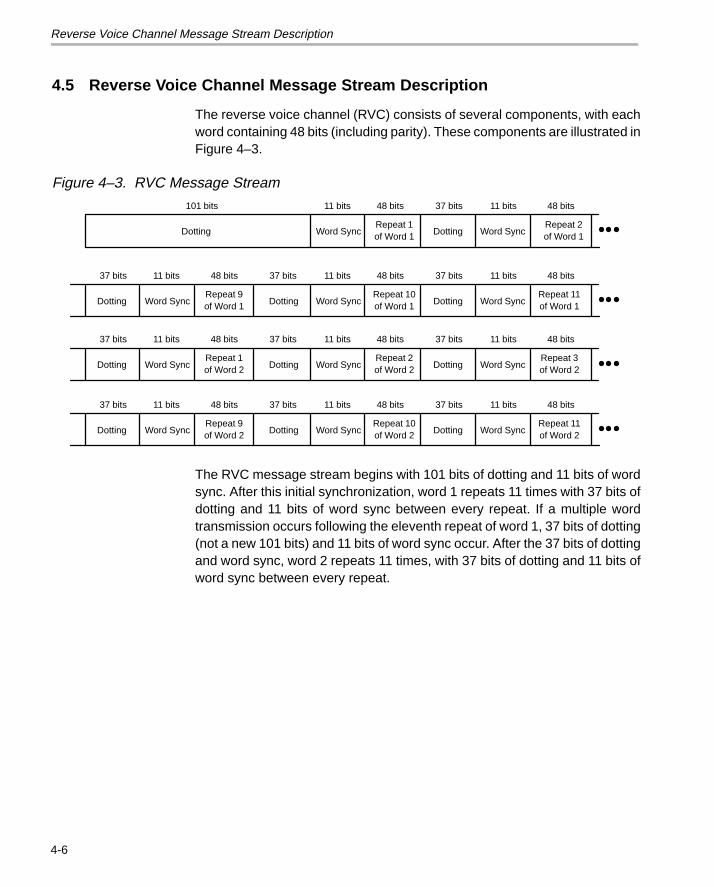
Reverse Voice Channel Message Stream Description
4-6
4.5 Reverse Voice Channel Message Stream Description
The reverse voice channel (RVC) consists of several components, with eachword containing 48 bits (including parity). These components are illustrated inFigure 4–3.
Figure 4–3. RVC Message Stream
Dotting Word SyncRepeat 9of Word 1
37 bits
Repeat 10of Word 1Dotting Word Sync Dotting Word Sync
Repeat 11of Word 1
11 bits 48 bits 37 bits 11 bits 48 bits 37 bits 11 bits 48 bits
Repeat 1of Word 1Dotting Word Sync Dotting Word Sync
Repeat 2of Word 1
11 bits 48 bits 37 bits 11 bits 48 bits
Dotting Word SyncRepeat 1of Word 2
37 bits
Repeat 2of Word 2Dotting Word Sync Dotting Word Sync
Repeat 3of Word 2
11 bits 48 bits 37 bits 11 bits 48 bits 37 bits 11 bits 48 bits
Dotting Word SyncRepeat 9of Word 2
37 bits
Repeat 10of Word 2Dotting Word Sync Dotting Word Sync
Repeat 11of Word 2
11 bits 48 bits 37 bits 11 bits 48 bits 37 bits 11 bits 48 bits
101 bits
The RVC message stream begins with 101 bits of dotting and 11 bits of wordsync. After this initial synchronization, word 1 repeats 11 times with 37 bits ofdotting and 11 bits of word sync between every repeat. If a multiple wordtransmission occurs following the eleventh repeat of word 1, 37 bits of dotting(not a new 101 bits) and 11 bits of word sync occur. After the 37 bits of dottingand word sync, word 2 repeats 11 times, with 37 bits of dotting and 11 bits ofword sync between every repeat.
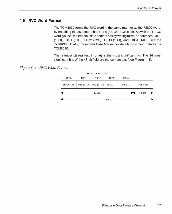
RVC Word Format
4-7Wideband Data Reverse Channel
4.6 RVC Word Format
The TCM8030 forms the RVC word in the same manner as the RECC word,by encoding the 36 content bits into a (48, 36) BCH code. As with the RECCword, you set the transmit data content bits by writing to write addresses TXD0(10H), TXD1 (11H), TXD2 (12H), TXD3 (13H), and TXD4 (14H). See theTCM8030 Analog Baseband Data Manual for details on writing data to theTCM8030.
The leftmost bit (earliest in time) is the most significant bit. The 36 mostsignificant bits of the 48-bit field are the content bits (see Figure 4–4).
Figure 4–4. RVC Word Format
Bits 35 – 28
TXD0
Parity Bits
36 Bits
48 Bits
TXD1
Bits 27 – 20
TXD2
Bits 19 – 12
TXD3
Bits 11 – 4
TXD4
Bits 3 – 0
12 Bits
RECC Transmit Data
5-1
Wideband Data Transmission
This chapter describes TCM8030 wideband data transmissions and provideswideband data transmission examples for both the reverse control andreverse voice channels.
Topic Page
5.1 Wideband Transmission Overview 5-2. . . . . . . . . . . . . . . . . . . . . . . . . . . . . .
5.2 Reverse Control Channel (RECC) Wideband Data Transmission 5-3. .
5.3 Reverse Voice Channel (RVC) Wideband Data Transmission 5-9. . . . . .
5.4 Wideband Data Transmission Precautions 5-15. . . . . . . . . . . . . . . . . . . . .
Chapter 5
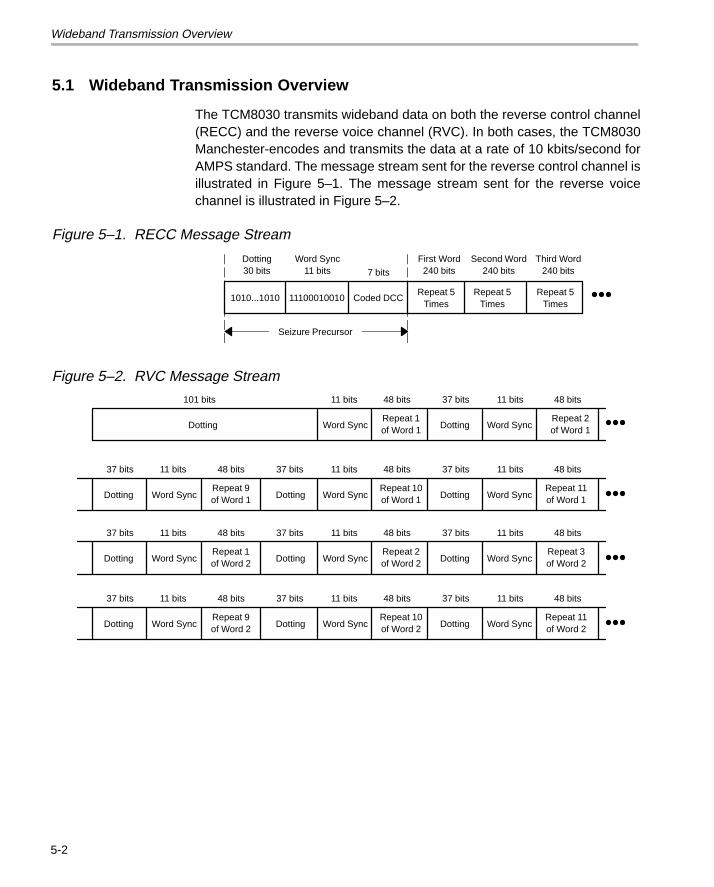
Wideband Transmission Overview
5-2
5.1 Wideband Transmission Overview
The TCM8030 transmits wideband data on both the reverse control channel(RECC) and the reverse voice channel (RVC). In both cases, the TCM8030Manchester-encodes and transmits the data at a rate of 10 kbits/second forAMPS standard. The message stream sent for the reverse control channel isillustrated in Figure 5–1. The message stream sent for the reverse voicechannel is illustrated in Figure 5–2.
Figure 5–1. RECC Message Stream
1010...1010 11100010010
Dotting30 bits
Repeat 5Times
Word Sync11 bits 7 bits
Coded DCC
First Word240 bits
Seizure Precursor
Repeat 5Times
Second Word240 bits
Repeat 5Times
Third Word240 bits
Figure 5–2. RVC Message Stream
Dotting Word SyncRepeat 9of Word 1
37 bits
Repeat 10of Word 1Dotting Word Sync Dotting Word Sync
Repeat 11of Word 1
11 bits 48 bits 37 bits 11 bits 48 bits 37 bits 11 bits 48 bits
Repeat 1of Word 1Dotting Word Sync Dotting Word Sync
Repeat 2of Word 1
11 bits 48 bits 37 bits 11 bits 48 bits
Dotting Word SyncRepeat 1of Word 2
37 bits
Repeat 2of Word 2Dotting Word Sync Dotting Word Sync
Repeat 3of Word 2
11 bits 48 bits 37 bits 11 bits 48 bits 37 bits 11 bits 48 bits
Dotting Word SyncRepeat 9of Word 2
37 bits
Repeat 10of Word 2Dotting Word Sync Dotting Word Sync
Repeat 11of Word 2
11 bits 48 bits 37 bits 11 bits 48 bits 37 bits 11 bits 48 bits
101 bits
Reverse Control Channel (RECC) Wideband Data Transmission
5-3Wideband Data Transmission
5.2 Reverse Control Channel (RECC) Wideband Data Transmission
The reverse control channel can be formed for either single- or multiple-wordtransmissions. Depending on which is necessary, certain procedures need tobe followed. These are described in the tables that follow.
5.2.1 Setup Procedures
When transmitting data on the reverse control channel, use the setupprocedures detailed in Table 5–1.
Table 5–1. Setup Procedures for Wide-Band Data Transmission on RECC
Address Data Description
0×0D 0×00 Reset TCM8030 (Only use reset when initially poweringon the phone — not at the beginning of everytransmission — or use when it is necessary to reset thephone.)
0×00 0×01 C1 – AMPS, RECC
0×06 0×?? IE2, Enable necessary interrupts
0×03 0×15 C4, Full operation, DTMF off
0×05 0×?? IE1 – Enable necessary interrupts
0×33 0×18 TX voice, TX data enabled at TXSUM
Note: 0×?? indicates user selection of data.
5.2.2 Write to TX Buffer
Write WORD 1 data to TX buffer (TXD0–TDX4) as detailed in Table 5–2.
Table 5–2. Write to TX Buffer
Address Data Description
0×10 0×?? Write word 1, bits 35–28 to TXD0.
0×11 0×?? Write word 1, bits 27–20 to TXD1.
0×12 0×?? Write word 1, bits 19–12 to TXD2.
0×13 0×?? Write word 1, bits 11–4 to TXD3.
0×14 0×?? Write word 1, bits 3–0 (LSBs) to TXD4.
Note: 0×?? indicates user selection of data.
5.2.3 Commence Transmission
When the commence transmission executes, TCM8030 transmits theManchester-encoded data on the control channel at a rate of 10 kbits/secondfor AMPS standard.
Reverse Control Channel (RECC) Wideband Data Transmission
5-4
Table 5–3. Commence Transmission
Address Data Description
0×08 0×00 Initiate transmission.
5.2.4 Single-Word Transmission
Form the single-word-transmission data stream as follows:
1) 30 bits of dotting, 11 bits of word sync, 7 bits coded DCC, 240 bits (word1 repeated five times)
2) Write to interrupt control word 1 (write address 05H, bit 3) to enable thetransmission-complete interrupt. After the fifth repeat occurs, the trans-mission-complete interrupt generates on INTRPT (pin 2).
3) Read event 1 (E1, read address 05H) and event 2 (E2, read address 06H)to clear the interrupt.
4) After clearing, you may write a new word to the TX buffer for anothersingle-word transmission.
5.2.5 Multiple-Word Transmission
When transmitting multiple words on the reverse control channel, use thesame setup procedures as the single-word transmission, but use the TXbuffer-available interrupt rather than the transmission-complete interrupt, asfollows:
1) Write a one to interrupt control word 1 (write address 05H, bit 1) to enablethe TX buffer-available interrupt.
2) After word 1 begins to transmit, an interrupt will appear on INTRPT (pin2), indicating that the TX buffer is available.
3) Read event 1 (E1, read address 05H) and event 2 (E2, read address 06H)to clear the interrupt.
4) After clearing, begin writing word 2 to the TX data buffer.
A TX commence is not required after writing word 2 to the TX data buffer. Thissequence is detailed in Table 5–4.
Reverse Control Channel (RECC) Wideband Data Transmission
5-5Wideband Data Transmission
Table 5–4. Write to TX Buffer
Address Data Description
0×05 0×?? INTRPT event read address E1
0×06 0×?? INTRPT event read address E2
0×10 0×?? Write word 2, bits 35–28 to TXD0
0×11 0×?? Write word 2, bits 27–20 to TXD1
0×12 0×?? Write word 2, bits 19–12 to TXD2
0×13 0×?? Write word 2, bits 11–4 to TXD3
0×14 0×?? Write word 2, bits 3–0 (LSBs) to TXD4
Note: 0×?? indicates user selection of data.
To transmit word 3, follow the same procedure as indicated for word 2.
The following sequence continues the transmission after the fifth repeat ofword 1:
1) 30 bits of dotting, 11 bits of word sync, 7 bits of coded DCC, 240 bits (word1 repeated five times)
2) 240 bits (word 2 repeated five times)
3) 240 bits (word 3 repeated five times), etc.
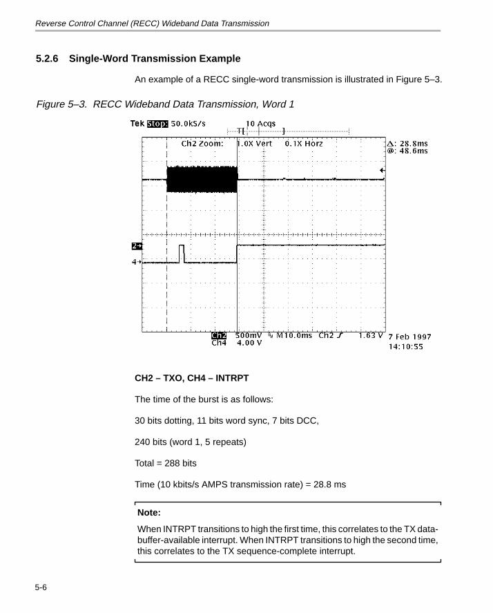
Reverse Control Channel (RECC) Wideband Data Transmission
5-6
5.2.6 Single-Word Transmission Example
An example of a RECC single-word transmission is illustrated in Figure 5–3.
Figure 5–3. RECC Wideband Data Transmission, Word 1
CH2 – TXO, CH4 – INTRPT
The time of the burst is as follows:
30 bits dotting, 11 bits word sync, 7 bits DCC,
240 bits (word 1, 5 repeats)
Total = 288 bits
Time (10 kbits/s AMPS transmission rate) = 28.8 ms
Note:
When INTRPT transitions to high the first time, this correlates to the TX data-buffer-available interrupt. When INTRPT transitions to high the second time,this correlates to the TX sequence-complete interrupt.
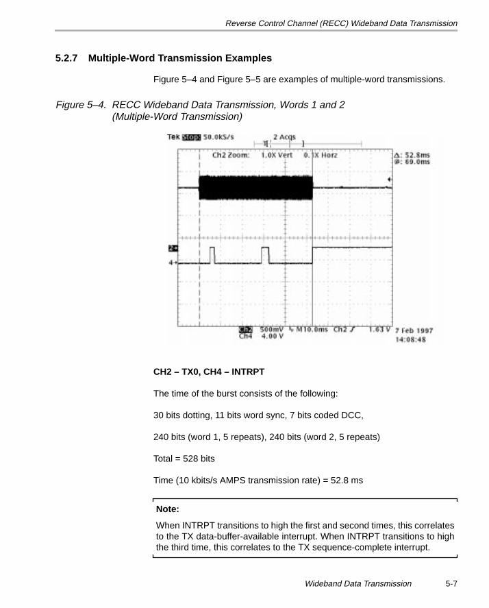
Reverse Control Channel (RECC) Wideband Data Transmission
5-7Wideband Data Transmission
5.2.7 Multiple-Word Transmission Examples
Figure 5–4 and Figure 5–5 are examples of multiple-word transmissions.
Figure 5–4. RECC Wideband Data Transmission, Words 1 and 2 (Multiple-Word Transmission)
CH2 – TX0, CH4 – INTRPT
The time of the burst consists of the following:
30 bits dotting, 11 bits word sync, 7 bits coded DCC,
240 bits (word 1, 5 repeats), 240 bits (word 2, 5 repeats)
Total = 528 bits
Time (10 kbits/s AMPS transmission rate) = 52.8 ms
Note:
When INTRPT transitions to high the first and second times, this correlatesto the TX data-buffer-available interrupt. When INTRPT transitions to highthe third time, this correlates to the TX sequence-complete interrupt.
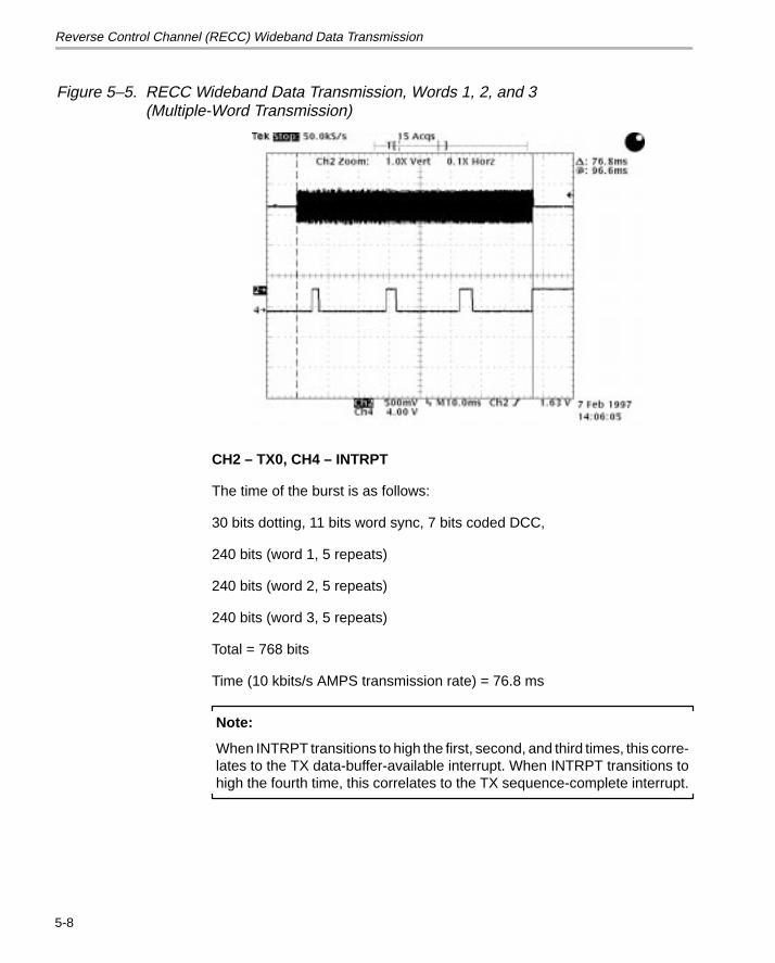
Reverse Control Channel (RECC) Wideband Data Transmission
5-8
Figure 5–5. RECC Wideband Data Transmission, Words 1, 2, and 3 (Multiple-Word Transmission)
CH2 – TX0, CH4 – INTRPT
The time of the burst is as follows:
30 bits dotting, 11 bits word sync, 7 bits coded DCC,
240 bits (word 1, 5 repeats)
240 bits (word 2, 5 repeats)
240 bits (word 3, 5 repeats)
Total = 768 bits
Time (10 kbits/s AMPS transmission rate) = 76.8 ms
Note:
When INTRPT transitions to high the first, second, and third times, this corre-lates to the TX data-buffer-available interrupt. When INTRPT transitions tohigh the fourth time, this correlates to the TX sequence-complete interrupt.
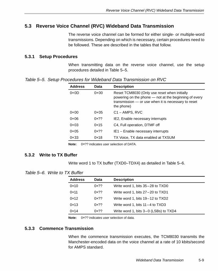
Reverse Voice Channel (RVC) Wideband Data Transmission
5-9Wideband Data Transmission
5.3 Reverse Voice Channel (RVC) Wideband Data Transmission
The reverse voice channel can be formed for either single- or multiple-wordtransmissions. Depending on which is necessary, certain procedures need tobe followed. These are described in the tables that follow.
5.3.1 Setup Procedures
When transmitting data on the reverse voice channel, use the setupprocedures detailed in Table 5–5.
Table 5–5. Setup Procedures for Wideband Data Transmission on RVC
Address Data Description
0×0D 0×00 Reset TCM8030 (Only use reset when initiallypowering on the phone — not at the beginning of everytransmission — or use when it is necessary to resetthe phone)
0×00 0×05 C1 – AMPS, RVC
0×06 0×?? IE2, Enable necessary interrupts
0×03 0×15 C4, Full operation, DTMF off
0×05 0×?? IE1 – Enable necessary interrupts
0×33 0×18 TX Voice, TX data enabled at TXSUM
Note: 0×?? indicates user selection of DATA.
5.3.2 Write to TX Buffer
Write word 1 to TX buffer (TXD0–TDX4) as detailed in Table 5–6.
Table 5–6. Write to TX Buffer
Address Data Description
0×10 0×?? Write word 1, bits 35–28 to TXD0
0×11 0×?? Write word 1, bits 27–20 to TXD1
0×12 0×?? Write word 1, bits 19–12 to TXD2
0×13 0×?? Write word 1, bits 11–4 to TXD3
0×14 0×?? Write word 1, bits 3–0 (LSBs) to TXD4
Note: 0×?? indicates user selection of data.
5.3.3 Commence Transmission
When the commence transmission executes, the TCM8030 transmits theManchester-encoded data on the voice channel at a rate of 10 kbits/secondfor AMPS standard.
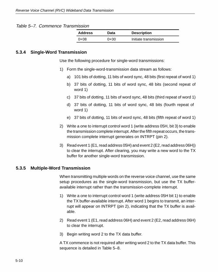
Reverse Voice Channel (RVC) Wideband Data Transmission
5-10
Table 5–7. Commence Transmission
Address Data Description
0×08 0×00 Initiate transmission
5.3.4 Single-Word Transmission
Use the following procedure for single-word transmissions:
1) Form the single-word-transmission data stream as follows:
a) 101 bits of dotting, 11 bits of word sync, 48 bits (first repeat of word 1)
b) 37 bits of dotting, 11 bits of word sync, 48 bits (second repeat ofword 1)
c) 37 bits of dotting, 11 bits of word sync, 48 bits (third repeat of word 1)
d) 37 bits of dotting, 11 bits of word sync, 48 bits (fourth repeat of word 1)
e) 37 bits of dotting, 11 bits of word sync, 48 bits (fifth repeat of word 1)
2) Write a one to interrupt control word 1 (write address 05H, bit 3) to enablethe transmission complete interrupt. After the fifth repeat occurs, the trans-mission complete interrupt generates on INTRPT (pin 2).
3) Read event 1 (E1, read address 05H) and event 2 (E2, read address 06H))to clear the interrupt. After clearing, you may write a new word to the TXbuffer for another single-word transmission.
5.3.5 Multiple-Word Transmission
When transmitting multiple words on the reverse voice channel, use the samesetup procedures as the single-word transmission, but use the TX buffer-available interrupt rather than the transmission-complete interrupt.
1) Write a one to interrupt control word 1 (write address 05H bit 1) to enablethe TX buffer-available interrupt. After word 1 begins to transmit, an inter-rupt will appear on INTRPT (pin 2), indicating that the TX buffer is avail-able.
2) Read event 1 (E1, read address 06H) and event 2 (E2, read address 06H)to clear the interrupt.
3) Begin writing word 2 to the TX data buffer.
A TX commence is not required after writing word 2 to the TX data buffer. Thissequence is detailed in Table 5–8.
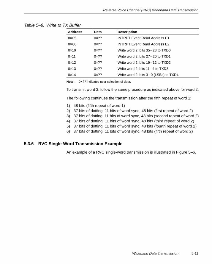
Reverse Voice Channel (RVC) Wideband Data Transmission
5-11Wideband Data Transmission
Table 5–8. Write to TX Buffer
Address Data Description
0×05 0×?? INTRPT Event Read Address E1
0×06 0×?? INTRPT Event Read Address E2
0×10 0×?? Write word 2, bits 35–28 to TXD0
0×11 0×?? Write word 2, bits 27–20 to TXD1
0×12 0×?? Write word 2, bits 19–12 to TXD2
0×13 0×?? Write word 2, bits 11–4 to TXD3
0×14 0×?? Write word 2, bits 3–0 (LSBs) to TXD4
Note: 0×?? indicates user selection of data.
To transmit word 3, follow the same procedure as indicated above for word 2.
The following continues the transmission after the fifth repeat of word 1:
1) 48 bits (fifth repeat of word 1)2) 37 bits of dotting, 11 bits of word sync, 48 bits (first repeat of word 2)3) 37 bits of dotting, 11 bits of word sync, 48 bits (second repeat of word 2)4) 37 bits of dotting, 11 bits of word sync, 48 bits (third repeat of word 2)5) 37 bits of dotting, 11 bits of word sync, 48 bits (fourth repeat of word 2)6) 37 bits of dotting, 11 bits of word sync, 48 bits (fifth repeat of word 2)
5.3.6 RVC Single-Word Transmission Example
An example of a RVC single-word transmission is illustrated in Figure 5–6.
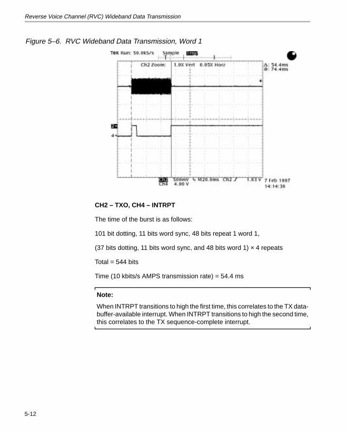
Reverse Voice Channel (RVC) Wideband Data Transmission
5-12
Figure 5–6. RVC Wideband Data Transmission, Word 1
CH2 – TXO, CH4 – INTRPT
The time of the burst is as follows:
101 bit dotting, 11 bits word sync, 48 bits repeat 1 word 1,
(37 bits dotting, 11 bits word sync, and 48 bits word 1) × 4 repeats
Total = 544 bits
Time (10 kbits/s AMPS transmission rate) = 54.4 ms
Note:
When INTRPT transitions to high the first time, this correlates to the TX data-buffer-available interrupt. When INTRPT transitions to high the second time,this correlates to the TX sequence-complete interrupt.
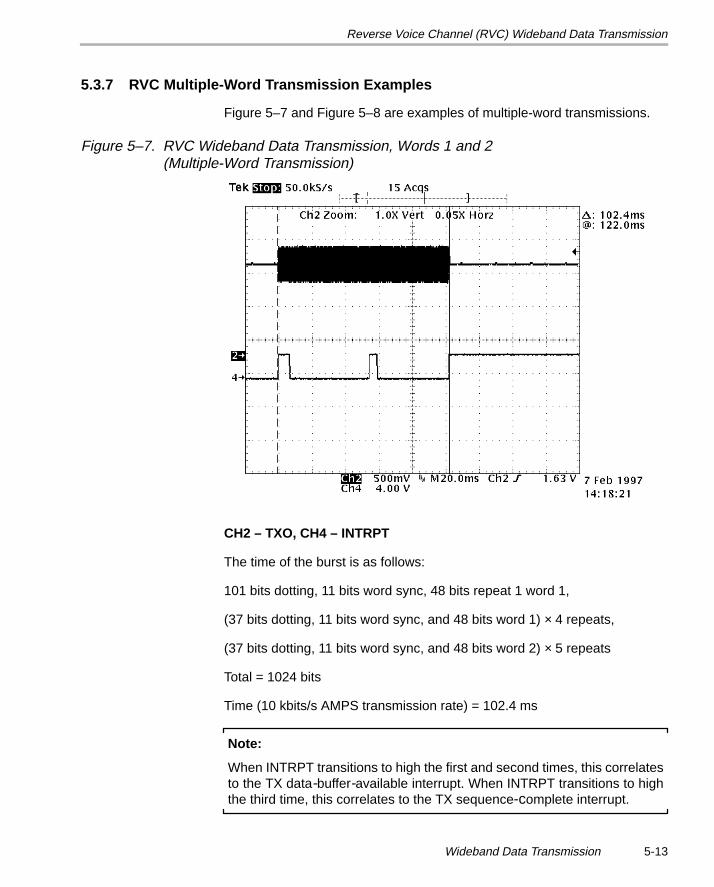
Reverse Voice Channel (RVC) Wideband Data Transmission
5-13Wideband Data Transmission
5.3.7 RVC Multiple-Word Transmission Examples
Figure 5–7 and Figure 5–8 are examples of multiple-word transmissions.
Figure 5–7. RVC Wideband Data Transmission, Words 1 and 2 (Multiple-Word Transmission)
CH2 – TXO, CH4 – INTRPT
The time of the burst is as follows:
101 bits dotting, 11 bits word sync, 48 bits repeat 1 word 1,
(37 bits dotting, 11 bits word sync, and 48 bits word 1) × 4 repeats,
(37 bits dotting, 11 bits word sync, and 48 bits word 2) × 5 repeats
Total = 1024 bits
Time (10 kbits/s AMPS transmission rate) = 102.4 ms
Note:
When INTRPT transitions to high the first and second times, this correlatesto the TX data-buffer-available interrupt. When INTRPT transitions to highthe third time, this correlates to the TX sequence-complete interrupt.
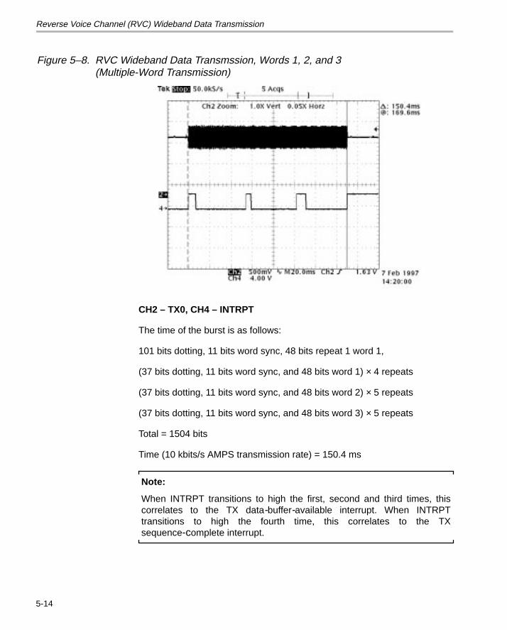
Reverse Voice Channel (RVC) Wideband Data Transmission
5-14
Figure 5–8. RVC Wideband Data Transmssion, Words 1, 2, and 3 (Multiple-Word Transmission)
CH2 – TX0, CH4 – INTRPT
The time of the burst is as follows:
101 bits dotting, 11 bits word sync, 48 bits repeat 1 word 1,
(37 bits dotting, 11 bits word sync, and 48 bits word 1) × 4 repeats
(37 bits dotting, 11 bits word sync, and 48 bits word 2) × 5 repeats
(37 bits dotting, 11 bits word sync, and 48 bits word 3) × 5 repeats
Total = 1504 bits
Time (10 kbits/s AMPS transmission rate) = 150.4 ms
Note:
When INTRPT transitions to high the first, second and third times, thiscorrelates to the TX data-buffer-available interrupt. When INTRPTtransitions to high the fourth time, this correlates to the TXsequence-complete interrupt.
Reverse Voice Channel (RVC) Wideband Data Transmission
5-15Wideband Data Transmission
5.4 Wideband Data Transmission Precautions
The TCM8030 wideband data transmission operates as designed. However,unless you use the correct procedures, the device may not behave asexpected. If transmitting one word of data, use the TX sequence-completeinterrupt before sending a second burst. This ends the message stream for thefirst word before any additional message streams start.
If transmitting multiple words, use the TX buffer-available interrupt to indicatethat the TX buffer is available. The TX buffer-available interrupt allows multiplewords to occur in a single-transmission message stream, in accordance withthe IS-91 Mobile Station – Base Station Compatibility Standard for 800-MHzAnalog Cellular.
After you observe this interrupt, clear the interrupt event registers (IE1 andIE2). After clearing, you can write bits 35–0 to the data buffers (TXD0–TXD4).In either the RECC or RVC, the proper transmission of word 2 begins after thelast repeat of word 1, without the need for a new commence transmission. Ifyou use the commence transmission, the formatting of the message streamwill restart and corrupt prior data.
In addition to performing a RECC transmission using the TCM8030, considerthe channel seizure procedure that the mobile station must follow to ensurea correct seizure. This procedure is covered in Chapter 6, Reverse ControlChannel Arbitration Processing.
6-1
Reverse Control Channel ArbitrationProcessing
This chapter describes the process and methods used during reverse controlchannel arbitration.
Topic Page
6.1 Reverse Control Channel Arbitration Processing Overview 6-2. . . . . . .
6.2 RECC Arbitration Methods 6-3. . . . . . . . . . . . . . . . . . . . . . . . . . . . . . . . . . . . .
Chapter 6
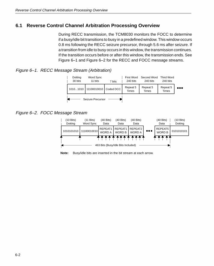
Reverse Control Channel Arbitration Processing Overview
6-2
6.1 Reverse Control Channel Arbitration Processing Overview
During RECC transmission, the TCM8030 monitors the FOCC to determineif a busy/idle bit transitions to busy in a predefined window. This window occurs0.8 ms following the RECC seizure precursor, through 5.6 ms after seizure. Ifa transition from idle to busy occurs in this window, the transmission continues.If the transition occurs before or after this window, the transmission ends. SeeFigure 6–1 and Figure 6–2 for the RECC and FOCC message streams.
Figure 6–1. RECC Message Stream (Arbitration)
1010...1010 11100010010
Dotting30 bits
Repeat 5Times
Word Sync11 bits 7 bits
Coded DCC
First Word240 bits
Seizure Precursor
Repeat 5Times
Second Word240 bits
Repeat 5Times
Third Word240 bits
Figure 6–2. FOCC Message Stream
1010101010 11100010010REPEAT1WORD A
REPEAT1WORD B
REPEAT2WORD A
REPEAT5WORD B 0101010101
463 Bits (Busy/Idle Bits Included)
(10 Bits)Dotting
(11 Bits)Word Sync
(40 Bits)Data
Note: Busy/idle bits are inserted in the bit stream at each arrow.
(40 Bits)Data
(40 Bits)Data
(40 Bits)Data
(10 Bits)Dotting
RECC Arbitration Methods
6-3Reverse Control Channel Arbitration Processing
6.2 RECC Arbitration Methods
Several methods may be implemented during RECC arbitration processing.
6.2.1 Software Control Arbitration
Control word 1 (write address 00H, bit 4): Writing 0 to this address placesarbitration processing under software control. In this case, when arbitrationfailure occurs, event register 1 (read address 05H, bit 2) and statusregister 1 (read address 00H, bit 2) indicate failure. In addition, if interruptcontrol register 1 (write address 05H, bit 2) is 1, an interrupt generates onINTRPT (TCM8030 device pin 2).
6.2.2 Hardware Control Arbitration
Control word 1 (write address 00H, bit 4): Writing one to this address performstwo functions. First, it enables software control arbitration, as defined above.Second, it disables TXRFEN and TXO when arbitration failure occurs. Only anarbitration reset (write address 0EH) can re-enable TXRFEN.
Control word 3 (write address 02H, bit 2): Controls the signal polarity ofTXRFEN and RXRFEN (Only TXRFEN applies to arbitration failure)
Write address 02H (bit 2) = 0: Active high (low indicates arbitration failure,see the following note)
Note:
Since TXRFEN and RXRFEN are open-drain drivers with active pulldownresistors, you must apply an external pullup resistor to pull the TXRFEN andRXRFEN signals high.
Write address 02H (bit 2) = 1: Active low (high indicates arbitration failure)
6.2.3 One or Two Busy/Idle Bits Observed
Control word 5 (write address 04H, bit 0): Controls the number of busy/idle bitsobserved.
Write address 04H (bit 0) = 0: One busy/idle bit observed. The windowoccurs from RECC TX bit 56 to bit 104.
RECC Arbitration Methods
6-4
Write address 04H (bit 0) = 1: Two busy/idle bits are observed in arbitrationprocessing. This requires the window to move 10 bits. This window occursfrom RECC TX bit 66 to bit 114, due to the first busy bit indicated 10 bitsprior to the second busy bit.
Monitoring the busy/idle bit transition using two busy/idle bits is more accuratethan monitoring the transition with one. It reduces the occurrence of FOCCrandom glitches that erroneously indicate a busy state when there actually isnone.
7-1
Automatic Frequency Control
This chapter defines automatic frequency control and its system cycle.
Topic Page
7.1 Automatic Frequency Control Overview 7-2. . . . . . . . . . . . . . . . . . . . . . . .
7.2 AFC Reference 7-3. . . . . . . . . . . . . . . . . . . . . . . . . . . . . . . . . . . . . . . . . . . . . . .
7.3 AFC System Concept 7-4. . . . . . . . . . . . . . . . . . . . . . . . . . . . . . . . . . . . . . . . . .
7.4 AFC Sample Cycle Detailed Description 7-5. . . . . . . . . . . . . . . . . . . . . . . .
Chapter 7
Automatic Frequency Control Overview
7-2
7.1 Automatic Frequency Control Overview
The TCM8030 provides the internal circuitry for automatic frequency control(AFC) of an external temperature-compensated crystal oscillator (TCXO).AFC reduces any error in the TCXO frequency so that in a closed-loop system,the relative frequency of the TCXO adheres to the IF frequency requirement.The TCXO frequency must have minimal frequency errors: many componentsand circuits within a mobile phone, such as frequency synthesizers,microcontrollers, and data processors, are referenced to this frequency.
AFC Reference
7-3Automatic Frequency Control
7.2 AFC Reference
The second IF frequency of the mobile phone receive section is the referencefor the AFC circuitry. The second IF frequency is derived from the receive RF(RXRF) signal. This signal is generated at the cell base station using frequencyreferences with tolerances less than 1 ppm. Because TCXO-referencedsynthesizers derive the second IF frequency from the RXRF signal, TCXOfrequency deviations can be corrected using a closed-loop system.
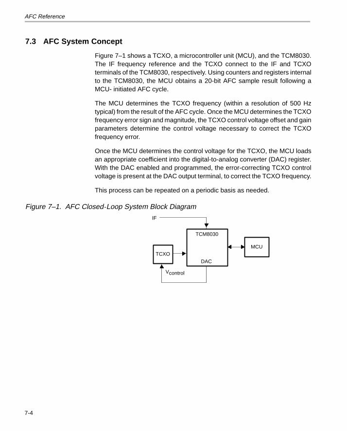
AFC Reference
7-4
7.3 AFC System Concept
Figure 7–1 shows a TCXO, a microcontroller unit (MCU), and the TCM8030.The IF frequency reference and the TCXO connect to the IF and TCXOterminals of the TCM8030, respectively. Using counters and registers internalto the TCM8030, the MCU obtains a 20-bit AFC sample result following aMCU- initiated AFC cycle.
The MCU determines the TCXO frequency (within a resolution of 500 Hztypical) from the result of the AFC cycle. Once the MCU determines the TCXOfrequency error sign and magnitude, the TCXO control voltage offset and gainparameters determine the control voltage necessary to correct the TCXOfrequency error.
Once the MCU determines the control voltage for the TCXO, the MCU loadsan appropriate coefficient into the digital-to-analog converter (DAC) register.With the DAC enabled and programmed, the error-correcting TCXO controlvoltage is present at the DAC output terminal, to correct the TCXO frequency.
This process can be repeated on a periodic basis as needed.
Figure 7–1. AFC Closed-Loop System Block Diagram
TCM8030
MCUTCXO
DAC
Vcontrol
IF
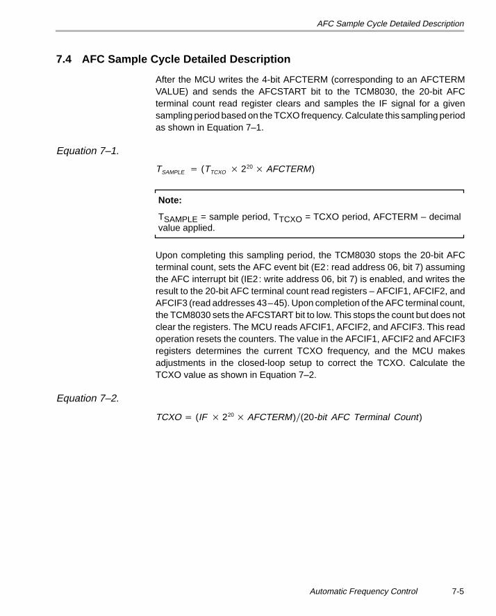
AFC Sample Cycle Detailed Description
7-5Automatic Frequency Control
7.4 AFC Sample Cycle Detailed Description
After the MCU writes the 4-bit AFCTERM (corresponding to an AFCTERMVALUE) and sends the AFCSTART bit to the TCM8030, the 20-bit AFCterminal count read register clears and samples the IF signal for a givensampling period based on the TCXO frequency. Calculate this sampling periodas shown in Equation 7–1.
Equation 7–1.
TSAMPLE (TTCXO 220 AFCTERM)
Note:
TSAMPLE = sample period, TTCXO = TCXO period, AFCTERM – decimalvalue applied.
Upon completing this sampling period, the TCM8030 stops the 20-bit AFCterminal count, sets the AFC event bit (E2: read address 06, bit 7) assumingthe AFC interrupt bit (IE2: write address 06, bit 7) is enabled, and writes theresult to the 20-bit AFC terminal count read registers – AFCIF1, AFCIF2, andAFCIF3 (read addresses 43–45). Upon completion of the AFC terminal count,the TCM8030 sets the AFCSTART bit to low. This stops the count but does notclear the registers. The MCU reads AFCIF1, AFCIF2, and AFCIF3. This readoperation resets the counters. The value in the AFCIF1, AFCIF2 and AFCIF3registers determines the current TCXO frequency, and the MCU makesadjustments in the closed-loop setup to correct the TCXO. Calculate theTCXO value as shown in Equation 7–2.
Equation 7–2.
TCXO (IF 220 AFCTERM)(20-bit AFC Terminal Count)
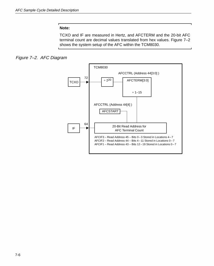
AFC Sample Cycle Detailed Description
7-6
Note:
TCXO and IF are measured in Hertz, and AFCTERM and the 20-bit AFCterminal count are decimal values translated from hex values. Figure 7–2shows the system setup of the AFC within the TCM8030.
Figure 7–2. AFC Diagram
÷ 220 AFCTERM[3:0]
÷ 1–15
AFCSTART
AFCCTRL (Address 44[4] )
20-Bit Read Address forAFC Terminal Count
AFCCTRL (Address 44[3:0] )
AFCIF3 – Read Address 45 – Bits 0 – 3 Stored in Locations 4 – 7AFCIF2 – Read Address 44 – Bits 4 – 11 Stored in Locations 0 – 7AFCIF1 – Read Address 43 – Bits 12 – 19 Stored in Locations 0 – 7
TCM8030
72
64
TCXO
IF
AFC Sample Cycle Detailed Description
7-7Automatic Frequency Control
Table 7–1 describes the AFC 20-bit terminal count read address controlexecution.
Table 7–1. AFC 20-Bit Terminal Count Read Address Control Execution
Operation Description
Apply IF signal (450-kHz typical value), apply TCXO signal, 14.85-MHz typical value.
Write to address 31H–0×04. Enables CLKOUT terminal to verify TCXO signalentering AFC circuitry. CLKSEL must be tied highexternally to observe TCXO on CLKOUT. This is only forobservation purposes and does not have to beimplemented for AFC operation (see Note 3).
Write to address 06H (bit 7). Enables AFC interrupt by writing 1 to bit 7
Write to address 44H (bits 0–3). Sets AFCTERM = 0×?? (see Note 2)
Write to address 44H (bit 4). AFCSTART = 1 starts AFC count/AFCSTART = 0 stopsAFC count (see Note 1).
AFC terminal count begins.
AFC terminal value reached. Resets AFCSTART.
AFC terminal count is written to AFCIF1, AFCIF2,and AFCIF3.
AFC has reached terminal count interrupt. Event interrupt (read address 06H bit 7) is set andINTRPT (device pin 2) is generated.
Microcontroller reads the 20-bit AFC terminal count. Reads in the following order at addresses 43 (8-bit), 44(8-bit), and 45 (4-bit, bits 4–7).
Apply this AFC terminal count read address toEquation 2 to verify TCXO frequency.
Notes: 1) For AFC execution to commence, IFAMP must be enabled – write address 30 H (bit 4).
2) The AFCTERM 4-bit register can range from 1 to 15 (01H to 0FH). The TCXO frequency can be resolved with oneAFC sample period (AFCTERM = 1). Multiples of one AFC sample period can be used to find an average TCXOfrequency error by setting the AFCTERM to a value greater than one.
3) In this case, TCXO is also the TCM8030 clocking scheme. CLKSEL must be high, and the TCXO frequency mustbe one of those indicated in Table 2–2. If TCXO is not selected as the TCM8030 clocking scheme, another schememust be selected with CLKSEL low. Then the AFC circuit can operate with any frequency less than 20 MHz. SeeSection 2.6, Clocks, for additional clocking scheme information.
8-1
Keyboard Interface and Set Monitoring
This chapter provides basic information regarding the programmableexpansion input/output (I/O) ports PIO3, PIO2, and PIO1. It also describes thespecial function port keys 3–0 of the PIO3 I/O port, as well as supplies readand write register definitions and a microcontroller and keyboard interfacingdiagram.
Topic Page
8.1 Keyboard Interface and Set Monitoring Overview 8-2. . . . . . . . . . . . . . . .
8.2 Keyboard Interrupt Inputs [KEY3:KEY0] 8-3. . . . . . . . . . . . . . . . . . . . . . . .
8.3 TCM8030 8-Bit Programmable Expansion I/O Ports 8-5. . . . . . . . . . . . . .
Chapter 8
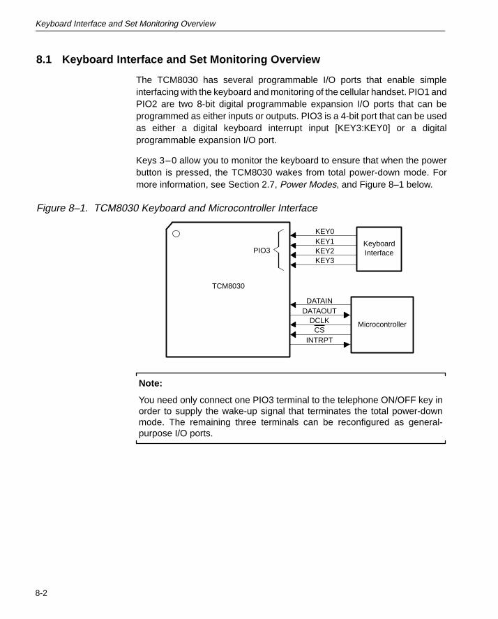
Keyboard Interface and Set Monitoring Overview
8-2
8.1 Keyboard Interface and Set Monitoring Overview
The TCM8030 has several programmable I/O ports that enable simpleinterfacing with the keyboard and monitoring of the cellular handset. PIO1 andPIO2 are two 8-bit digital programmable expansion I/O ports that can beprogrammed as either inputs or outputs. PIO3 is a 4-bit port that can be usedas either a digital keyboard interrupt input [KEY3:KEY0] or a digitalprogrammable expansion I/O port.
Keys 3–0 allow you to monitor the keyboard to ensure that when the powerbutton is pressed, the TCM8030 wakes from total power-down mode. Formore information, see Section 2.7, Power Modes, and Figure 8–1 below.
Figure 8–1. TCM8030 Keyboard and Microcontroller Interface
KEY0KEY1KEY2KEY3
DATAINDATAOUT
DCLKCS
INTRPT
KeyboardInterface
Microcontroller
PIO3
TCM8030
Note:
You need only connect one PIO3 terminal to the telephone ON/OFF key inorder to supply the wake-up signal that terminates the total power-downmode. The remaining three terminals can be reconfigured as general-purpose I/O ports.
Keyboard Interrupt Inputs [KEY3:KEY0]
8-3Keyboard Interface and Set Monitoring
8.2 Keyboard Interrupt Inputs [KEY3:KEY0]
You can implement the TCM8030 PIO3 programmable I/O port as a keyboardinterrupt input. Write to the PIO control word, PIOC3 (address 19H), which setsup the PIO3 direction (input/output). After the direction initializes as an input,set the PIO3 pullup control, PI3PULL (address 1BH). Finally, to send aninterrupt to the microcontroller when the keyboard power-on button is on, setthe PIO3 interrupt control PI3INT (address 1CH) as an interrupt port. Thisinterrupt will occur on event register 2, E2 (read address 06H, bit 6).
Write to interrupt control word 2 (IE2: write address 06H, bit 6) to enable thePIO3 input-port sensed signal interrupt to appear on INTRPT (TCM8030device terminal 2).
8.2.1 PIO Control Word (PIOC3 – Write Address 19H)
PIOC3 selects whether PIO3 is an input or an output as shown in Table 8–1.In order to use PIO3 as the keyboard scan, you need to define PIO3 as aninput.
Table 8–1. PIO Control Word – PIOC3
ValueCorresponding Terminal Function
0 Input
1 Output
8.2.2 PIO3 Pullup Enabling (PI3PULL – Write Address 1BH)
When set to one, bits 0 to 3 of this register activate small pullup transistors thatdrive inputs using open-drain drivers. After a reset, the ports (PIO3) configureas inputs and the pullup transistors are enabled.
8.2.3 PIO3 Interrupt Control (PI3INT – Write Address 1CH)
PI3INT serves two purposes. First, PI3INT bits 0–3 set an interrupt when asignal is sensed on PIO3. Second, PI3INT bits 4–7 set the polarity of theinterrupt (active high or active low). See Table 8–2 and Table 8–3 below.
Table 8–2. PIO3 Interrupt Control (PI3INT, Bits 3–0) Definition
PI3INT Bit (0–3) Function
0 PIO3 operates as a normal port.
1Signal sensed on PIO3 causesinterrupt when IE2.6 is high.
Keyboard Interrupt Inputs [KEY3:KEY0]
8-4
Table 8–3. PIO3 Interrupt Control (PI3INT, Bits 7–4) Definition
PI3INT Bit (4–7) Function
0 Active low interrupt
1 Active high interrupt
8.2.4 Event Register 2 (E2 – Read Address 06) Bit 6
The E2 register is eight bits wide and maintains the status of certain interruptflags. For the PIO3 input-sensed signal, this status is E2 – bit 6. These flagsindicate which events occurred since the previous read transaction, regard-less of their associated interrupt control bits. The microcontroller must read E2after E1 because of protocol for queuing and clearing events. The eventregisters clear following a read transaction. Since there are two registers, thefollowing protocol occurs:
1) The microcontroller addresses E1.
2) The INTRPT terminal goes low, the contents of both interrupt registerstransfer to buffers, and the registers clear to catch new events.
3) The serial microcontroller interface clocks out the buffered eventinformation.
4) Any new events are caught in the main interrupt register; however, at thistime INTRPT remains low.
5) The microcontroller addresses E2.
6) The buffered E2 information, caught in step 2, clocks out.
7) Once the read transaction is complete, INTRPT goes high if any interruptsoccurred during steps 2 through 6. The event register now contains allevents that occurred during the read transaction.
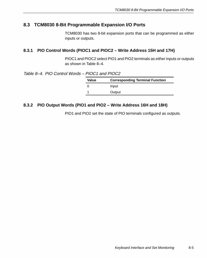
TCM8030 8-Bit Programmable Expansion I/O Ports
8-5Keyboard Interface and Set Monitoring
8.3 TCM8030 8-Bit Programmable Expansion I/O Ports
TCM8030 has two 8-bit expansion ports that can be programmed as eitherinputs or outputs.
8.3.1 PIO Control Words (PIOC1 and PIOC2 – Write Address 15H and 17H)
PIOC1 and PIOC2 select PIO1 and PIO2 terminals as either inputs or outputsas shown in Table 8–4.
Table 8–4. PIO Control Words – PIOC1 and PIOC2
Value Corresponding Terminal Function
0 Input
1 Output
8.3.2 PIO Output Words (PIO1 and PIO2 – Write Address 16H and 18H)
PIO1 and PIO2 set the state of PIO terminals configured as outputs.
9-1
Typical Analog Cellular Telephone Processing
This chapter describes the baseband processing techniques to applynecessary external circuitry to the TCM8030.
Topic Page
9.1 Typical Analog Cellular Telephone System Overview 9-2. . . . . . . . . . . . .
9.2 Circuit Description 9-3. . . . . . . . . . . . . . . . . . . . . . . . . . . . . . . . . . . . . . . . . . . .
9.3 Decoupling on Supply Lines 9-7. . . . . . . . . . . . . . . . . . . . . . . . . . . . . . . . . . .
9.4 Decoupling TXVMID and RXVMID 9-8. . . . . . . . . . . . . . . . . . . . . . . . . . . . . . .
9.5 Microphone Grounding 9-9. . . . . . . . . . . . . . . . . . . . . . . . . . . . . . . . . . . . . . . .
9.6 Suggested Trim Adjustment Sequence 9-10. . . . . . . . . . . . . . . . . . . . . . . .
Chapter 9
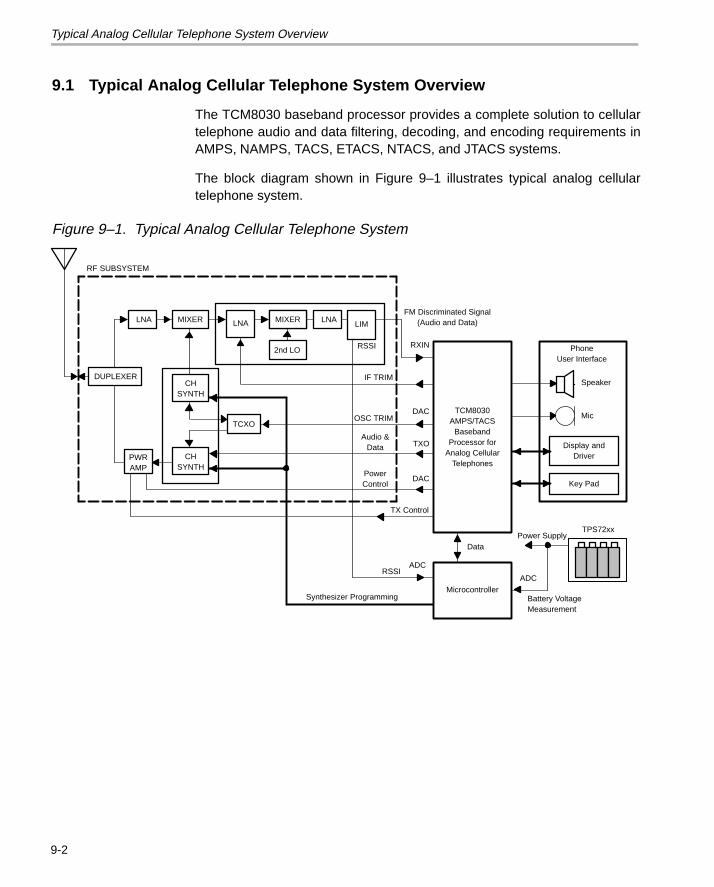
Typical Analog Cellular Telephone System Overview
9-2
9.1 Typical Analog Cellular Telephone System Overview
The TCM8030 baseband processor provides a complete solution to cellulartelephone audio and data filtering, decoding, and encoding requirements inAMPS, NAMPS, TACS, ETACS, NTACS, and JTACS systems.
The block diagram shown in Figure 9–1 illustrates typical analog cellulartelephone system.
Figure 9–1. Typical Analog Cellular Telephone System
TCM8030AMPS/TACS
BasebandProcessor for
Analog CellularTelephones
PhoneUser Interface
Speaker
Display andDriver
Mic
Key Pad
Microcontroller
Power Supply
ADC
Battery VoltageMeasurement
Data
LNA MIXER LNA MIXERMIXER
2nd LO
LNALIM
DUPLEXER
RSSI
CHSYNTH
CHSYNTH
TCXO
PWRAMP
FM Discriminated Signal(Audio and Data)
RF SUBSYSTEM
RXIN
IF TRIM
OSC TRIM
Audio &Data
PowerControl
TX Control
DAC
TXO
DAC
RSSI
Synthesizer Programming
ADC
TPS72xx
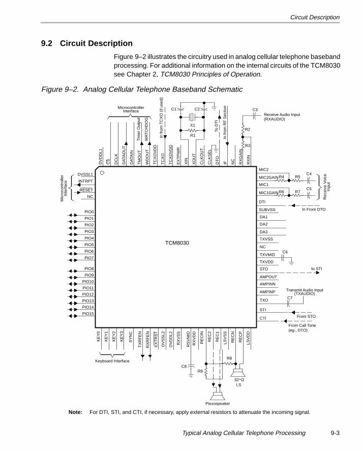
Circuit Description
9-3Typical Analog Cellular Telephone Processing
9.2 Circuit Description
Figure 9–2 illustrates the circuitry used in analog cellular telephone basebandprocessing. For additional information on the internal circuits of the TCM8030see Chapter 2, TCM8030 Principles of Operation.
Figure 9–2. Analog Cellular Telephone Baseband SchematicD
VD
DL1
CS
DC
LK
DA
TAO
UT
DA
TAIN
TM
OU
T
WD
OU
T
TC
XO
VD
D
TC
XO
TC
XO
VD
D
EX
TP
WR
XIN
XO
UT
CLK
OU
T
CLK
SE
L
DT
O
IF NC
RX
GA
IN
RX
IN
KE
Y0
KE
Y1
KE
Y2
KE
Y3
SY
NC
TX
RF
EN
RX
RF
EN
EX
TR
ST
DV
SS
L2
DV
DD
L2
RX
VS
S
RS
VM
IDR
XV
DD
RE
CIN
RE
C2
RE
C1
LSV
SS
RE
CN
RE
CP
LSV
DD
R8
R9C8
DVSSL1
INTRPT
RESET
NC
Mic
roco
ntro
ller
Inte
rfac
e
Rec
eive
Voi
ceIn
put
In From DTO
to STI
C6
LS
Piezospeaker
Keyboard Interface
PIO0
PIO1
PIO2
PIO3
PIO4
PIO5
PIO6
PIO7
PIO8
PIO9
PIO10
PIO11
PIO12
PIO13
PIO14
PIO15
MIC2
MIC2GAIN
MIC1
MIC1GAIN
DTI
SUBVSS
DA1
DA2
DA3
TXVSS
NC
TXVMID
TXVDD
STO
AMPOUT
AMPINN
AMPINP
TXO
STI
CTI
C1 C2
R2
R3
C3
In fr
om T
CX
O (
if us
ed)
In fr
om R
F S
ectio
n
To D
TI
Receive Audio Input(RXAUDIO)
MicrocontrollerInterface
Tim
er O
utpu
t
WA
TC
HD
OG
From STO
C7
From Call Tone(eg., DTO)
Transmit Audio Input(TXAUDIO)
R4 R5C4
R6 R7C5
TCM8030
X1
R1
32-Ω
Note: For DTI, STI, and CTI, if necessary, apply external resistors to attenuate the incoming signal.
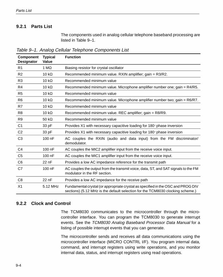
Parts List
9-4
9.2.1 Parts List
The components used in analog cellular telephone baseband processing arelisted in Table 9–1.
Table 9–1. Analog Cellular Telephone Components List
ComponentDesignator
TypicalValue
Function
R1 1 MΩ Biasing resistor for crystal oscillator
R2 10 kΩ Recommended minimum value. RXIN amplifier; gain = R3/R2.
R3 10 kΩ Recommended minimum value
R4 10 kΩ Recommended minimum value. Microphone amplifier number one; gain = R4/R5.
R5 10 kΩ Recommended minimum value
R6 10 kΩ Recommended minimum value. Microphone amplifier number two; gain = R6/R7.
R7 10 kΩ Recommended minimum value
R8 10 kΩ Recommended minimum value. REC amplifier; gain = R8/R9.
R9 50 kΩ Recommended minimum value
C1 33 pF Provides X1 with necessary capacitive loading for 180phase inversion
C2 33 pF Provides X1 with necessary capacitive loading for 180phase inversion
C3 100 nF AC couples the RXIN (audio and data input) from the FM discriminator/demodulator.
C4 100 nF AC couples the MIC2 amplifier input from the receive voice input.
C5 100 nF AC couples the MIC1 amplifier input from the receive voice input.
C6 22 nF Provides a low AC impedance reference for the transmit path
C7 100 nF AC couples the output from the transmit voice, data, ST, and SAT signals to the FMmodulator in the RF section.
C8 22 nF Provides a low AC impedance for the receive path
X1 5.12 MHz Fundamental crystal (or appropriate crystal as specified in the OSC and PROG DIVsections) (5.12 MHz is the default selection for the TCM8030 clocking scheme.)
9.2.2 Clock and Control
The TCM8030 communicates to the microcontroller through the micro-controller interface. You can program the TCM8030 to generate interruptevents. See the TCM8030 Analog Baseband Processor Data Manual for alisting of possible interrupt events that you can generate.
The microcontroller sends and receives all data communications using themicrocontroller interface (MICRO CONTRL I/F). You program internal data,command, and interrupt registers using write operations, and you monitorinternal data, status, and interrupt registers using read operations.
Transmit Path
9-5Typical Analog Cellular Telephone Processing
9.2.3 Transmit Path
The transmit voice inputs, MIC1 and MIC2, feed a pair of microphoneamplifiers. Outputs from these amplifiers feed back into MICGAIN1 andMICGAIN2. An applied external resistor pair sets the gain for each amplifier.
The TCM8030 uses a single power supply. The reference voltage TXVMIDbiases the inputs of the microphone amplifiers, MIC1 and MIC2.
The voice, wideband or narrowband data, signaling tone (ST), and supervisoryaudio tone (SAT) signal levels are programmable throughout the transmitpath, therefore eliminating the need for external adjustments.
The TCM8030 data encoder, TX ENCODER, performs all necessary controland voice channel signal formatting before it transmits the digital signal to thetransmit output (TXO).
In wideband mode, the TCM8030 produces a digitally filtered signal, phase-locked to the received SAT signal. This received digital SAT signal is firstseparated from any signal noise and then measured and regenerated.
In narrowband mode, the received signal is continuously compared to theDSAT word. The DSAT word is regarded as correctly detected and determineswhen the receiver is locked onto the voice channel. The DSAT circuit in theTCM8030 generates the DSAT that corresponds to the DSAT color codingindependent of the DSAT received from the base station.
For both SAT and DSAT, the TCM8030 conditions the digital signal and outputsthe signal at TXO transmit output.
Along with the SAT, the TCM8030 also transmits a 10-kHz signaling tone (ST)on the voice channel to confirm channel orders and to request a flash-hook bythe mobile, mobile-alert, or mobile-ending call. The TCM8030 outputs thissignal at TXO transmit output. From TXO, the TCM8030 connects the audiosignal to the RF modulator section.
9.2.4 Receive Path
The output from the FM demodulator/discriminator connects to the receiveinput (RXIN) of the TCM8030.
The TCM8030 audio outputs, REC1 and REC2, can be used as two separateoutputs. For example, one can drive the phone earpiece, and the other candrive test equipment or accessories such as a hands-free unit. These twoaudio outputs can otherwise be configured to provide a differential output inorder to increase the maximum level.
Digital-to-Analog Converters
9-6
The TCM8030 filters and converts the received data to a digital signal. Inwideband mode, after this data recovery, the data processor majority-votesand error-corrects the data. In narrowband mode, after this data recovery, thedata processor error-corrects the data.
After data recovery, an interrupt signals the microcontroller that received datais available.
In addition to the data, the TCM8030 also recovers the SAT signal from the RXaudio path through a filter and comparator. This signal feeds to the TCM8030data processor where it is detected and regenerated.
9.2.5 Digital-to-Analog Converters
The TCM8030 contains three 8-bit DACs. The DAC outputs are at terminalsDAC1, DAC2, and DAC3. These DACs are all 8-bit linear digital-to-analogconverters. One provides power control of the RF transmit amplifier. The othertwo provide voltage adjustments to the RF stage for such purposes ascalibrating the temperature-compensated crystal oscillator (TCXO) andtrimming the first intermediate frequency (IF) stage.
9.2.6 Timers
The TCM8030 contains a watchdog timer and programmable timer. Thewatchdog timer resets the telephone’s microcontroller if a time-out conditionoccurs. This is a requirement of AMPS and TACS systems. An uncommittedprogrammable 8-bit timer has an output, TMOUT, that pulses low when thecounter reaches zero.
9.2.7 Keyboard Scan
The TCM8030 has a 4-bit port that accepts inputs from a keyboard andgenerates interrupts to the microcontroller. This port can also be configuredas a general-purpose I/O port. One I/O terminal connected to the telephoneON/OFF key supplies a wake-up signal that terminates the total power-downmode.
9.2.8 I/O Expansion
The TCM8030 contains two 8-bit programmable expansion I/O ports. Theseare provided for communication with the telephone’s microcontroller. Each bitis programmable as either an output or an input, with optional, current sourcepullup resistors.
Decoupling on Supply Lines
9-7Typical Analog Cellular Telephone Processing
9.3 Decoupling on Supply Lines
The transmit supply (TXVDD and TXVSS), receive supply (RXVDD andRXVSS), digital 1 supply (DVDDL1 and DVSSL1), digital 2 supply (DVDDL2and DVSSL2), and TCXO supply (TCXOVDD and TCXOVSS) requiredecoupling. You can achieve this by applying a 0.1-µF ceramic and a 1.0-µFtantalum capacitor in parallel, between the previous source’s supply (VDD)and the ground (VSS). The values of these capacitors are minimumrecommended values.

Decoupling TXVMID and RXVMID
9-8
9.4 Decoupling TXVMID and RXVMID
TXVMID and RXVMID require separate decoupling from the supplies. You canachieve this by applying a 22-nF capacitor between RXVMID and RSVSS andalso between TXVMID and TXVSS. The values of these capacitors areminimum recommended values. Figure 9–3 illustrates this decoupling.
Figure 9–3. Decoupling TXVMID and RXVMID
TCM8030
TXVMID
TXVSS
22 nF
RXVMID
RXVSS
22 nF
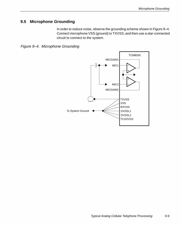
Microphone Grounding
9-9Typical Analog Cellular Telephone Processing
9.5 Microphone Grounding
In order to reduce noise, observe the grounding scheme shown in Figure 9–4.Connect microphone VSS (ground) to TXVSS, and then use a star-connectedcircuit to connect to the system.
Figure 9–4. Microphone Grounding
TCM8030
_
+
_+
TXVSSVSSRXVSS
DVSSL1
DVSSL2TCXOVSS
MICGAIN1
MIC1
MIC2
To System Ground
MICGAIN2
Suggested Trim Adjustment Sequence
9-10
9.6 Suggested Trim Adjustment Sequence
The TCM8030 is designed so that it requires no manual trims. All levels canbe adjusted to meet system requirements and to compensate for productiontolerances by writing to the microcontroller interface on the TCM8030. Themicrocontroller can then store the required data in a nonvolatile memory in thephone. When the phone is turned on, an initialization routine can write thiscalibrated data to the TCM8030.
The suggested sequence of adjustments is detailed below.
9.6.1 Transmit Adjustment Procedure
Voice Trim (VDTRIM) – Write Address 34H – [VD3 – VD0]
nominal setting [VD3 – VD0] = <1000>
1) Mute the signaling tone and SAT.
2) Apply an audio signal, at the desired level, into the amplifiers for MIC1 andMIC2.
3) Adjust VDTRIM register [VD3 – VD0] to set the frequency deviation. Thisalso adjusts the TX DTMF level.
DTMF Trim
Set the DTMF level by using external resistors between the DTO output andthe DTI input (TX path) and CTI input (RX path). There is not an independentDTMF trim register for the TCM8030.
Limiter Trim (LIMITER) – Write Address 35H – [LIM3 – LIM0]
nominal setting [LIM3 – LIM0] = <1010>
1) Increase the audio signal level by 20 dB.2) Adjust [LIM3 – LIM0] to produce the required maximum deviation.
SAT Trim (SATTRIM) – Write Address 36H – [SAT3 – SAT0]
nominal setting [SAT3 – SAT0] = <1000>
1) Turn off the signaling tone and turn on the SAT path.2) Make the TCM8030 generate its own 6000-Hz SAT tone.3) Adjust [SAT3 – SAT0] to give the required frequency deviation.
Suggested Trim Adjustment Sequence
9-11Typical Analog Cellular Telephone Processing
TX-DAT Trim – (TX-DAT TRIM) – Write Address 37H – [DAT2 – DAT0]
(NAMPS or NTACS)
nominal setting [DAT2 – DAT0] = <100>
1) Set the TCM8030 to transmit the signaling tone.2) Adjust [DAT2 – DAT0] for necessary narrowband data.
Transmit Trim (TXTRIM) – Write Address 38H – [TXT4 – TXT0]
nominal setting [TXT4 – TXT0] = <10000>
1) Set TX–DAT TRIM to nominal = 100.
2) Set the TCM8030 to transmit the signaling tone.
3) Adjust [TXT4 – TXT0] to set the frequency deviation to that required by theAMPS or TACS system.
9.6.2 Receive Adjustment Procedure
Receive Trim (RXTRIM) – Write Address 39H – [RXT3 – RXT0]
nominal setting [RXT3 – RXT0] = <1000>
1) Input a modulated signal to the telephone.2) Adjust [RXT3 – RXT0] to produce the required level at REC1 and REC2.
9.6.3 Muting the Audio Path
Transmit Path –
Writing 00H to TXCFG (write address 33H) mutes the TX path. The path isactually muted at two positions: TXSW and TXSUM by connecting to TXVMID.
Receive Path –
Writing 00H to RXCFG (write address 32H) mutes the RX path. The path isactually muted at two positions: REC1SW and RECBUF by connecting toRXVMID.
9.6.4 RF Stage Adjustment Procedure
DACs to Trim RF Sections
Use the three 8-bit DACs to trim sections of the RF stage.
1) Write to address 40H – DAC range select (DACRANGE): Each DAC canindependently set to full or half-range scale. For full range, the step sizeis TXVDD/256, and for half range, the step size is TXVDD/512.
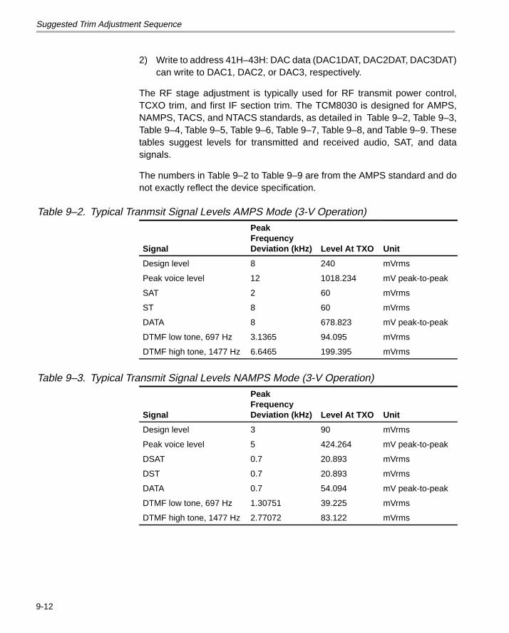
Suggested Trim Adjustment Sequence
9-12
2) Write to address 41H–43H: DAC data (DAC1DAT, DAC2DAT, DAC3DAT)can write to DAC1, DAC2, or DAC3, respectively.
The RF stage adjustment is typically used for RF transmit power control,TCXO trim, and first IF section trim. The TCM8030 is designed for AMPS,NAMPS, TACS, and NTACS standards, as detailed in Table 9–2, Table 9–3,Table 9–4, Table 9–5, Table 9–6, Table 9–7, Table 9–8, and Table 9–9. Thesetables suggest levels for transmitted and received audio, SAT, and datasignals.
The numbers in Table 9–2 to Table 9–9 are from the AMPS standard and donot exactly reflect the device specification.
Table 9–2. Typical Tranmsit Signal Levels AMPS Mode (3-V Operation)
Signal
Peak FrequencyDeviation (kHz) Level At TXO Unit
Design level 8 240 mVrms
Peak voice level 12 1018.234 mV peak-to-peak
SAT 2 60 mVrms
ST 8 60 mVrms
DATA 8 678.823 mV peak-to-peak
DTMF low tone, 697 Hz 3.1365 94.095 mVrms
DTMF high tone, 1477 Hz 6.6465 199.395 mVrms
Table 9–3. Typical Transmit Signal Levels NAMPS Mode (3-V Operation)
Signal
Peak FrequencyDeviation (kHz) Level At TXO Unit
Design level 3 90 mVrms
Peak voice level 5 424.264 mV peak-to-peak
DSAT 0.7 20.893 mVrms
DST 0.7 20.893 mVrms
DATA 0.7 54.094 mV peak-to-peak
DTMF low tone, 697 Hz 1.30751 39.225 mVrms
DTMF high tone, 1477 Hz 2.77072 83.122 mVrms
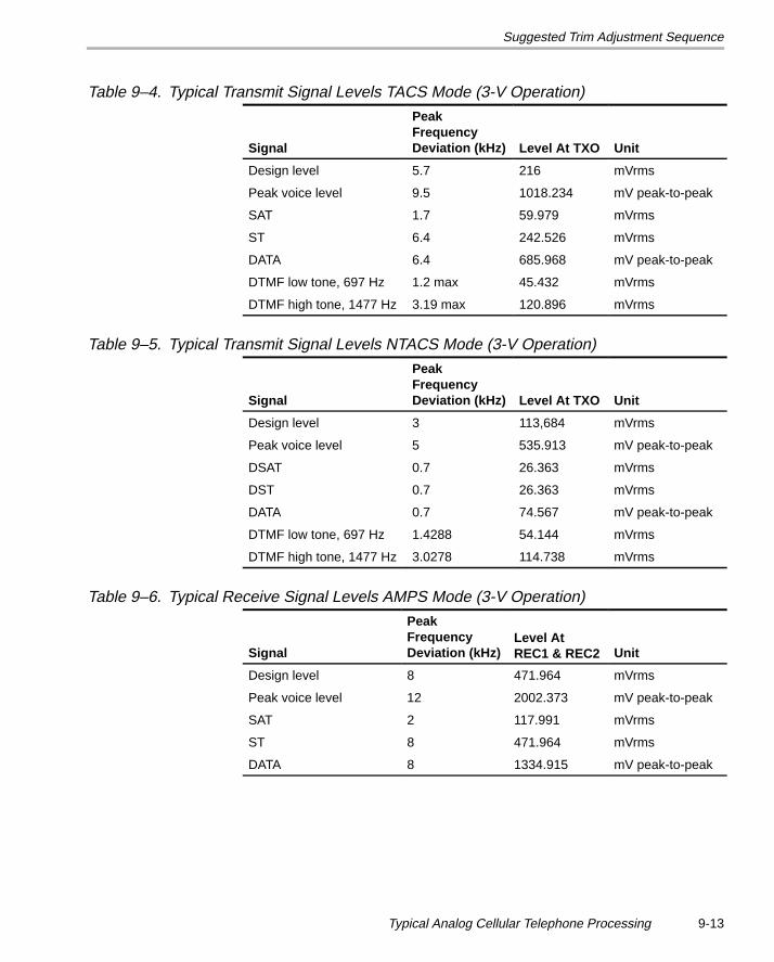
Suggested Trim Adjustment Sequence
9-13Typical Analog Cellular Telephone Processing
Table 9–4. Typical Transmit Signal Levels TACS Mode (3-V Operation)
Signal
Peak FrequencyDeviation (kHz) Level At TXO Unit
Design level 5.7 216 mVrms
Peak voice level 9.5 1018.234 mV peak-to-peak
SAT 1.7 59.979 mVrms
ST 6.4 242.526 mVrms
DATA 6.4 685.968 mV peak-to-peak
DTMF low tone, 697 Hz 1.2 max 45.432 mVrms
DTMF high tone, 1477 Hz 3.19 max 120.896 mVrms
Table 9–5. Typical Transmit Signal Levels NTACS Mode (3-V Operation)
Signal
Peak FrequencyDeviation (kHz) Level At TXO Unit
Design level 3 113,684 mVrms
Peak voice level 5 535.913 mV peak-to-peak
DSAT 0.7 26.363 mVrms
DST 0.7 26.363 mVrms
DATA 0.7 74.567 mV peak-to-peak
DTMF low tone, 697 Hz 1.4288 54.144 mVrms
DTMF high tone, 1477 Hz 3.0278 114.738 mVrms
Table 9–6. Typical Receive Signal Levels AMPS Mode (3-V Operation)
Signal
Peak FrequencyDeviation (kHz)
Level AtREC1 & REC2 Unit
Design level 8 471.964 mVrms
Peak voice level 12 2002.373 mV peak-to-peak
SAT 2 117.991 mVrms
ST 8 471.964 mVrms
DATA 8 1334.915 mV peak-to-peak
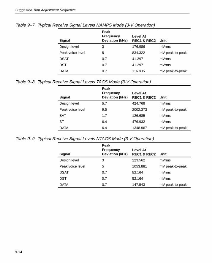
Suggested Trim Adjustment Sequence
9-14
Table 9–7. Typical Receive Signal Levels NAMPS Mode (3-V Operation)
Signal
Peak FrequencyDeviation (kHz)
Level AtREC1 & REC2 Unit
Design level 3 176.986 mVrms
Peak voice level 5 834.322 mV peak-to-peak
DSAT 0.7 41.297 mVrms
DST 0.7 41.297 mVrms
DATA 0.7 116.805 mV peak-to-peak
Table 9–8. Typical Receive Signal Levels TACS Mode (3-V Operation)
Signal
Peak FrequencyDeviation (kHz)
Level AtREC1 & REC2 Unit
Design level 5.7 424.768 mVrms
Peak voice level 9.5 2002.373 mV peak-to-peak
SAT 1.7 126.685 mVrms
ST 6.4 476.932 mVrms
DATA 6.4 1348.967 mV peak-to-peak
Table 9–9. Typical Receive Signal Levels NTACS Mode (3-V Operation)
Signal
Peak FrequencyDeviation (kHz)
Level AtREC1 & REC2 Unit
Design level 3 223.562 mVrms
Peak voice level 5 1053.881 mV peak-to-peak
DSAT 0.7 52.164 mVrms
DST 0.7 52.164 mVrms
DATA 0.7 147.543 mV peak-to-peak
A-1
Appendix A
Glossary
AAFC: Automatic Frequency Control. The closed loop process that calibrates
a TCXO frequency by using a more stable IF frequency as a reference.
AMPS: Advanced Mobile Phone Services
arbitration logic: A stage in the data processor that monitors the FOCC foran idle-to-busy transition to correlate messages sent on the corre-sponding RECC.
BBCH code: Bose-Chaudhuri-Hocquenghem Code.
BPF: Band-Pass Filter
busy-idle bits: The portion of the data stream transmitted by a land stationon a forward control channel that is used to indicate the current busy-idlestatus of the corresponding reverse control channel.
CCBSW: Compressor Bypass Switch
compandor: A combination of a compressor at the transmitter to reduce thedynamic range of the transmitted signal and an expandor at the receiverto recover this signal to the original dynamic range. Used incommunications systems to improve signal-to-noise as a result ofreduced transmitted dynamic range. In analog cellular, 2:1 syllabiccompression is used to limit the maximum peak voice deviation to±2.9 kHz.
control channel: A channel used for the transmission of digital controlinformation from a land station to a mobile station or from a mobile stationto a land station.
Appendix A

Glossary
A-2
CTI: Call Tone Input
DDAC: Digital-to-Analog Converter
DCC: Digital Color Code. A digital signal transmitted by a land station on aforward control channel that is used to detect capture of a land stationby an interfering mobile station.
de-emphasis: A stage in the receiver path that restores frequencycomponents to their original level.
dotting: A fixed frequency tone that corresponds the phase of the receiverclock to the rate of the incoming data.
DSAT: Digital Supervisory Audio Tone
DST: Digital Signaling Tone
DTI: DTMF Signaling Input
DTMF: Dual-Tone Multifrequency Generator
DTO: Dual-Tone Multifrequency Generator Output
EEBSW: Expandor Bypass Switch
ETACS: Extended Total Access Communication Systems
extended protocol: An optional expansion of the signaling messagesbetween the land station and mobile station to allow for the addition ofnew system features and operational capabilities.
FFOCC: Forward Control Channel. A control channel used from a land station
to a mobile station.
full operation mode: TCM8030 power mode where power is applied to thedevice, and the phone is in conversation mode. The DTMF generator canbe separately enabled along with several auxiliary functional blocks.
FVC: Forward Voice Channel. A voice channel used from a land station toa mobile station.
Glossary
A-3 Glossary
I
idle mode: TCM8030 power mode where power is applied to the device andthe device is monitoring the FOCC from the base station.
IF: Intermediate Frequency
J
JTACS: Japanese Total Access Communication Systems
L
land station: A station in the Domestic Public Cellular Radio Tele-communications Service, other than a mobile station, used for radiocommunications with mobile stations.
limiter: A stage in the receiver path that reduces amplitude variations in theincoming signal from the FM demodulator/discriminator.
LS DRIVER: Loudspeaker Driver
M
majority voting: A vote of three out of five words to determine whether toeliminate the recognition of corrupted data.
MCU: Microcontroller Unit
mobile station: A station in the Domestic Public Cellular Radio Tele-communications Service used while in motion or during halts atunspecified points. It is assumed that mobile stations include portableunits (e.g., hand-held “personal” units) as well as units installed invehicles.
N
NAMPS: Narrowband Advanced Mobile Phone Services
NTACS: Narrowband Total Access Communication Services
Glossary
A-4
P
PLL: Phase-Locked Loop
pre-emphasis: A stage in the transmitter path that optimizes the frequencycomponents of the audio signals for FM transmission.
R
RECC: Reverse Control Channel. The control channel used from a mobilestation to a land station.
RECC multiple-word transmission: Message format that continues thesecond word (240 bits) immediately following the completion of the firstword (240 bits) in a single, continuous RECC message stream. This canconsist of one to five words.
RFI: Radio Frequency Interference
RVC: Reverse Voice Channel. The voice channel used from a mobile stationto a land station.
RVC multiple-word transmission: Message format that continues thesecond word sequence immediately following the completion of the firstword sequence in a single, continuous RVC message stream. This canconsist of one or two words.
S
SAT: Supervisory Audio Tone. One of three tones in the 6-kilohertz regionthat are transmitted by a land station and transponded by a mobilestation.
seizure precursor: The initial digital sequence transmitted by a mobilestation to a land station on a reverse control channel.
shutdown mode: TCM8030 power savings mode where power is appliedto the device, but the phone is unable to answer calls.
signaling tone: A 10-kHz tone transmitted by a mobile station on a voicechannel to: (1) confirm orders, (2) signal flash requests, and (3) signalrelease requests.
SPI: Serial Peripheral Interface
Glossary
A-5 Glossary
ST: Signaling Tone
STI: Sidetone Input
synchronization: The process by which the data processor attempts tocorrelate its clock phase with the incoming received data stream.
T
TACS: Total Access Communication Systems
TCXO: Temperature-Compensated Crystal Oscillator
tone mode: TCM8030 power mode where power is applied to the device,the phone is not in communication with the base station, and the userinterface is enabled.
total power-down mode: TCM8030 power savings mode where all circuitsin the device are powered down except a static power-up.
TXBPF: Transmit Band-Pass Filter
TXLPF: Transmit Low-Pass Filter
TXO: Transmit Output
TXSW: Transmit Switch
TXVMID: Transmit Voltage Mid-rail Reference
V
voice channel: A channel on which a voice conversation occurs and onwhich brief digital messages may be sent from a land station to a mobilestation or from a mobile station to a land station.
W
word sync: An 11-bit Barker code (11100010010) that is used as part of theFOCC, RECC, FVC, and RVC preamble formats.
X
XTALOSC: Crystal Oscillator

Index
Index-2
digital data processing 2-2
digital keyboard interrupt input 8-2
digital programmable expansion I/O port 8-2
digital supervisory audio tone 1-3, 9-5detector circuit 2-26recovery circuit 2-2, 2-10, 2-26
switch 2-24
digital supervisory audio tone (DSATSW) 2-24
digital supervisory audio tone detector (DSATDET) 2-26
digital supervisory audio tone/digital signaling tonegenerator (DSAT/DST GEN) 2-24
digital-to-analog converter (DAC) 1-3, 2-11, 2-28,7-4, 9-6
DSAT 1-3, 2-2, 2-10, 2-24, 2-25, 2-26, 9-5
DST 2-24, 2-25
DTMF trim 9-10
dual-tone multifrequency generator (DTMF) 2-28
EETACS 1-2, 1-3, 2-2, 9-2
expandor bypass switch (EBSW) 2-23
extended total access communicationsystems 1-2, 9-2
external power-on reset mode 2-18
Ffine mode 3-5
FOCC 2-20
FOCC Frame Sync 3-5, 3-6, 3-7
FOCC message stream 6-2
forward control channel (FOCC) 2-20, 3-1, 3-2,3-4, 6-2, 6-4
forward control channel (FOCC) mode 3-5, 3-6
forward voice channel (FVC) 3-1, 3-2
forward voice channel (FVC) mode 3-8, 3-10, 3-11
frame synchronization (WORD SYNC) 2-25
full-operation mode 1-4, 2-20
FVC Frame Sync 3-10, 3-11, 3-12
FVC message stream 3-8, 3-9
Ggeneral purpose I/O port 9-6
II/O ports
digital programmable expansion 8-2general purpose 9-6programmable expansion 8-1, 8-2, 9-6
idle mode 1-4, 2-9, 2-20logic circuit 2-26
idle mode logic 2-9, 2-26idle submode 2-20independent output (DTO) 2-7internal clocking signals 2-11interrupt logic (INTRPT LOGIC) 2-29
JJTACS 1-2, 1-3, 2-2, 9-2
Kkeyboard scan 2-29
Llimiter circuit (LIMITER) 2-22limiter trim 9-10loudspeaker driver (LS DRIVER) 2-6, 2-11, 2-23
Mmajority voting 2-2, 2-9, 2-26, 3-2, 3-5, 3-9, 9-6messages
reverse control channel (RECC) 4-2reverse voice channel (RVC) 4-2
MIC1 amplifier 2-7, 2-21MIC2 amplifier 2-7, 2-21microcontroller interface (MICRO CONTRL
I/F) 2-29modes
coarse 3-5fine 3-5forward control channel (FOCC) 3-5, 3-6
Index
Index-3
forward voice channel (FVC) 3-8, 3-10, 3-11power
full-operation 1-4, 2-20idle 1-4, 2-20
idle submode 2-20shutdown 2-18, 2-19, 2-20total power-down 2-18, 2-19
shutdown 1-4tone 1-4total power-down 1-4, 2-13, 2-15, 2-20
power-on reset 2-18tone 2-20total power-down 8-2, 9-6
NNAMPS 1-2, 1-3, 2-2, 9-2, 9-12
narrowband advanced mobile phone services 1-2,9-2, 9-12
narrowband data attenuator (NB-DATATTEN) 2-25
narrowband data/DSAT recovery (NB-RXRECOVERY) 2-26
narrowband receive data/low-pass filter (NB-RXLPF) 2-25
narrowband receive/DSAT comparator (NB-RXCOMP) 2-25
narrowband total access communicationsystems 1-2, 9-2, 9-12
narrowband transmit data encoder (NB-TXENCODER) 2-24
NTACS 1-2, 1-3, 2-2, 9-2, 9-6, 9-12
Oorder confirmation message 4-2
order message 4-2
origination message 4-2
oscillator trim functions 2-11
Ppage response message 4-2
PIO Port 1 2-29
PIO Port 2 2-29
power modetotal power-down 8-2, 9-6
power-off logic 2-28power-on-reset circuit (RC) 2-18pre-emphasis circuit 2-22programmable expansion I/O ports 8-1, 8-2, 8-5,
9-6programmable timer 9-6
RRECC message stream 4-3, 6-2RECC messages
order 4-2order confirmation 4-2origination 4-2page response 4-2
RECC seizure precursor 4-3, 6-2receive 1 switch (REC1SW) 2-23receive amplifier circuit (RXAMP) 2-22receive audio path 2-6, 2-10, 2-20, 2-23
call tone input (CTI) 2-6independent output (DTO) 2-7receive buffer (RECBUF) 2-6receive summing block (RECSUM) 2-6sidetone input (STI) 2-6volume control (VOL CTRL) 2-6
receive band-pass filter (RXBPF) 2-23receive band-pass filter (RXSAT BPF) 2-27receive buffer (RECBUF) 2-6receive buffer (RX BUFFER) 2-26receive control (RX CONTROL) 2-26receive decoding 2-2receive path 2-2
audio 2-22audio outputs 9-5audio processing functions 2-22
de-emphasis 2-23expandor 2-23expandor bypass switch (EBSW) 2-23loud speaker driver 2-23receive 1 switch 2-23receive amplifier circuit (RXAMP) 2-22receive band-pass filter (RXBPF) 2-23receive trim (RXTRIM) 2-22receiver buffer 2-23receiver summing (RECSUM) 2-23
Index
Index-4
volume control (VOL CTRL) 2-23data processing functions 2-25
arbitration logic (ARBITRAT LOGIC) 2-26digital supervisory audio tone detector (DSAT
DET) 2-26frame synchronization (WORD SYNC) 2-25idle mode logic 2-26majority voting 2-26narrowband data/DSAT recovery (NB-RX
RECOVERY) 2-26narrowband receive data/low-pass filter (NB-
RX LPF) 2-25narrowband receive/DSAT comparator (NB-
RX LPF) 2-25receive buffer (RX BUFFER) 2-26receive control (RX CONTROL) 2-26sync word detect (SYNC WORD DET) 2-26wide-band data recovery (WB-RX
RECOVERY) 2-25wide-band receive comparator (WB-RX
COMP) 2-25wide-band/narrowband BCH decoder 2-26
SAT processing functions 2-27receive band-pass filter (RXSAT BPF) 2-27supervisory audio tone comparator (SAT
COMP) 2-27supervisory audio tone
processing functions 2-27
receive processingdata recovery 3-2forward control channel (FOCC) 3-1, 3-2, 3-4forward voice channel (FVC) 3-1, 3-2
receive summing block (RECSUM) 2-6
receive trim (RXTRIM) 2-22, 9-11
receive voltage mid-rail reference generator(RXVMID) 2-28
receiver buffer (RECBUF) 2-23
receiver summing (RECSUM) 2-23
reverse control channel (RECC) 4-1, 4-2, 4-3, 5-1,5-2, 5-3, 5-4, 6-1
reverse voice channel (RVC) 4-1, 4-2, 4-6, 5-1,5-2, 5-9, 5-10
RVC message stream 4-6
RVC messagesbase station challenge order 4-2called-address 4-2order confirmation 4-2unique challenge order confirmation 4-2
SSAT 1-3, 2-2, 2-8, 2-10, 2-26, 9-5
SAT processing functionsreceive path
supervisory audio tone 2-27transmit path 2-26
supervisory audio tone (SAT) 2-26SAT trim 9-10
seizure precursor, RECC 4-3
shutdown mode 1-4, 2-18, 2-19, 2-20
sidetone input (STI) 2-6
sidetone output (STO) 2-7
signaling tone 9-5
signalsdigital signaling tone (DST) 2-24, 2-25digital supervisory audio tone (DSAT) 2-10,
2-24, 2-25, 2-26internal clocking 2-11supervisory audio tone (SAT) 2-8
ST 9-5
standardsAMPS 4-2, 5-2, 5-3baseband processing
advanced mobile phone services(AMPS) 1-2, 1-3, 2-2, 9-2, 9-6, 9-12
extended total access communicationsystems (ETACS) 1-2, 1-3, 2-2, 9-2
Japanese total access communicationsystems (JTACS) 1-2, 1-3, 2-2, 9-2
narrowband advanced mobile phone services(NAMPS) 1-2, 1-3, 2-2, 9-2, 9-12
narrowband total access communicationsystems (NTACS) 1-2, 1-3, 2-2, 9-2, 9-6,9-12
total access communication systems(TACS) 1-2, 1-3, 2-2, 9-2, 9-12
supervisory audio tone 1-3, 2-2, 2-10, 9-5attenuator 2-27comparator 2-10generator/detector 2-27receive path
processing functions 2-27transmit path
processing functions 2-26trim circuit 2-27
supervisory audio tone attenuator (SATATTEN) 2-27
Index
Index-5
supervisory audio tone comparator (SATCOMP) 2-27
supervisory audio tone generator/detector (SATGEN/DET) 2-27
supervisory audio tone trim (SAT TRIM) 2-27
sync word detect (SYNC WORD DET) 2-26
TTACS 1-2, 1-3, 2-2, 9-2, 9-6, 9-12
TCXO 2-12, 2-13, 9-6, 9-7, 9-12
temperature-compensated crystal oscillator(TCXO) 2-12, 2-13, 7-2, 7-3, 7-4, 7-5, 7-7, 9-6,9-7, 9-12
timer 2-28
timersprogrammable 9-6watchdog 9-6
tone mode 1-4, 2-20
total access communication systems 1-2, 9-2, 9-12
total power-down mode 1-4, 2-13, 2-15, 2-18,2-19, 2-20, 8-2, 9-6
transmit audio path 2-7, 2-10sidetone output (STO) 2-7transmit band-pass filter (TXBPF) 2-7transmit data low-pass filter (TX-DAT LPF) 2-10transmit gain trim (TXTRIM) 2-8transmit low-pass filter (TXLPF) 2-7transmit summer/low-pass filter
(TXSUMLPF) 2-8voice/DTMF gain trim (V/D TRIM) 2-7
transmit audio sources 2-21
transmit band-pass filter (TXBPF) 2-7, 2-21
transmit band-pass filter (TXSAT BPF) 2-27
transmit buffer (TX BUFFER) 2-24
transmit data low-pass filter (TX-DAT LPF) 2-10,2-25
transmit data trim (TX-DAT TRIM) 2-25
transmit encoding 2-2
transmit gain trim (TXTRIM) 2-8
transmit low-pass filter (TXLPF) 2-7, 2-22
transmit path 2-2, 2-10audio 2-21audio processing functions 2-21
compressor 2-21
compressor bypass switch (CBSW) 2-21limiter 2-22MIC1 amplifier 2-21MIC2 amplifier 2-21pre-emphasis 2-22transmit band-pass filter (TXBPF) 2-21transmit low-pass filter (TXLPF) 2-22transmit summing/low-pass filter
(TXSUMLPF) 2-22transmit switch (TXSW) 2-21transmit trim 2-22voice/DTMF trim (V/D TRIM) 2-21
audio sources 2-21data processing functions 2-24
digital supervisory audio tone(DSATSW) 2-24
digital supervisory audio tone/digital signalingtone generator (DSAT/DST GEN) 2-24
narrowband data attenuator (NB-DATATTEN) 2-25
narrowband transmit data encoder (NB-TXENCODER) 2-24
transmit buffer (TX BUFFER) 2-24transmit data low-pass filter (TX-DAT
LPF) 2-25transmit data trim (TX DAT TRIM) 2-25wide-band and narrowband switches (WS/
NBSW) 2-24wide-band data attenuator (WB-DAT
ATTEN) 2-25wide-band transmit data encoder (WB-TX
ENCODER) 2-24SAT processing functions 2-26
supervisory audio tone attenuator (SATATTEN) 2-27
supervisory audio tone generator/detector(SAT GEN/DET) 2-27
supervisory audio tone trim (SAT TRIM) 2-27transmit band-pass filter (TXSAT BPF) 2-27
voice inputs 9-5
transmit summer/low-pass filter (TXSUMLPF) 2-8
transmit summing/low-pass filter(TXSUMLPF) 2-22
transmit switch (TXSW) 2-21
transmit trim (TXTRIM) 2-22, 9-11
transmit voltage mid-rail reference generator(TXVMID) 2-28
TX-DAT trim 9-11
Index
Index-6
Uunique challenge order confirmation 4-2
Vvoice inputs 9-5
voice trim 9-10
voice/DTMF gain trim (V/D TRIM) 2-7
voice/DTMF trim (V/D TRIM) 2-21
volume control (VOL CTRL) 2-6, 2-23
Wwatchdog timer 2-18, 2-19, 2-29, 9-6wide-band and narrowband switches (WB/
NBSW) 2-24wide-band data attenuator (WB-DAT ATTEN) 2-25wide-band data recovery (WB-RX
RECOVERY) 2-25wide-band receive comparator (WB-RX
COMP) 2-25wide-band transmit data encoder (WB-TX
ENCODER) 2-24WS Expected 3-5, 3-6, 3-7, 3-9, 3-11