Embed Size (px)
Citation preview
Analog Circuits and Systems Prof. K Radhakrishna Rao
Lecture 24: Active Filters
1
Review
� RC and RL low pass filters � First order and second order filters � Q of second order filters less than half � RLC second order filters of any Q � Low pass RLC Butterworth, Chebyschev and inverse Chebyschev
and Elliptic filter designs
2
Active Filters
� Limitations of passive RC filters can be addressed using active elements
� Approaches in using active elements in designing filters � Inductor simulation � The problem of large size of inductor can be resolved using active
devices and RC elements to simulate the inductor in a traditional RLC filter.
3
Active Filters (contd.,)
� Q enhancement by feedback � Q of a passive second order RC Filter can be enhanced using
feedback and amplification � Biquad � Simulate nth order differential equations using n-integrators and
summing amplifiers. A simulator of a second order differential equation is popularly known as Biquad.
� The traditional approaches to filter design through Q-enhancement and inductor simulation are increasingly replaced by Biquad method because of commercial availability of universal active filter blocks (UAF 42 and UF 10).
4
Active Filters: Inductor Simulation
� All filters used in base-band applications, particularly in telephony, require large valued inductances resulting in large sizes.
� These filters needed to be designed as active filters simulating large inductances using active devices.
5
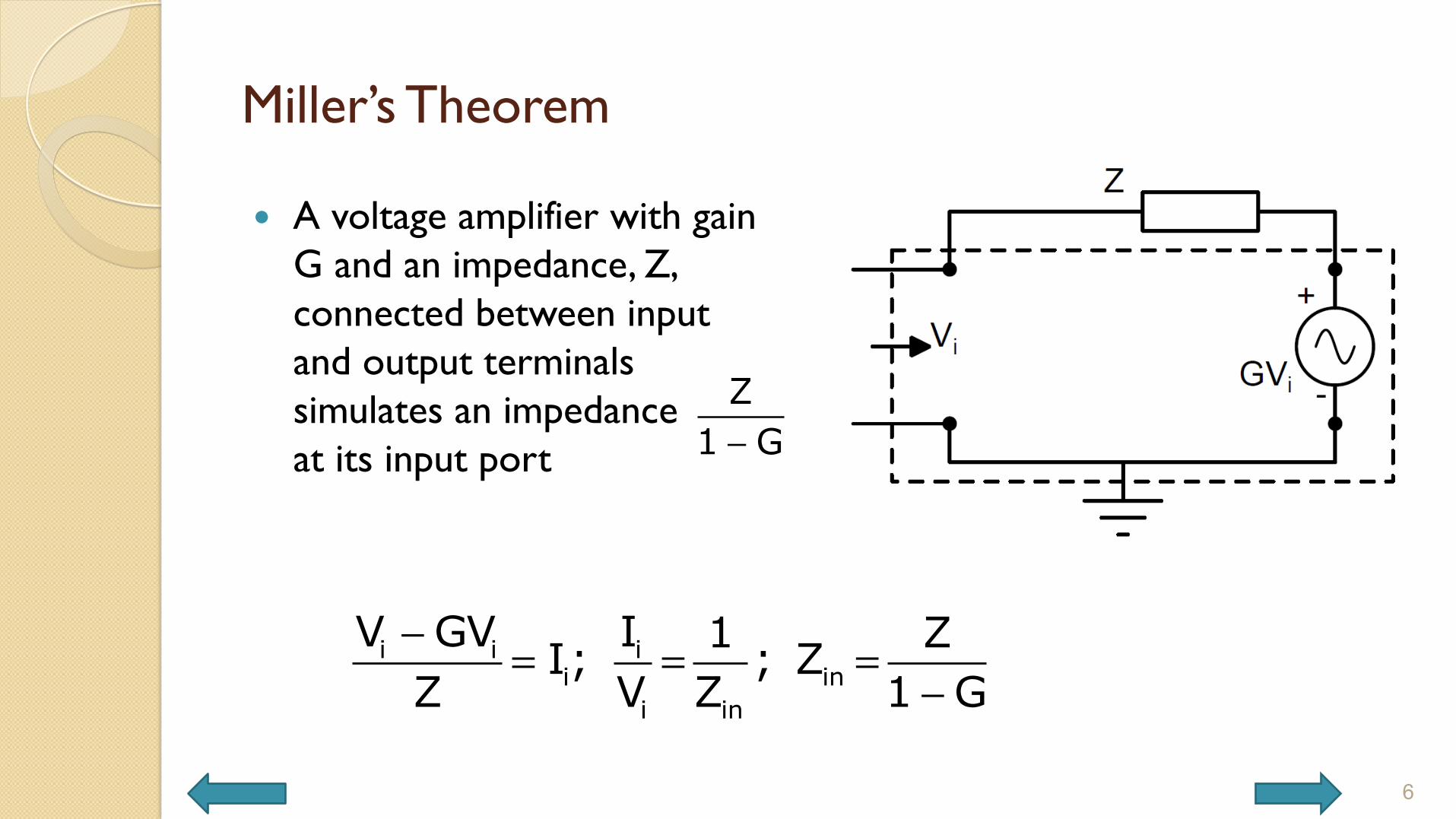
Miller’s Theorem
� A voltage amplifier with gain G and an impedance, Z, connected between input and output terminals simulates an impedance at its input port
6
i i ii in
i in
V GV I 1 ZI; ; ZZ V Z 1 G−
= = =−
Z1 G−
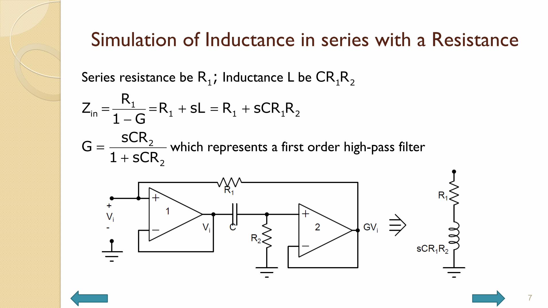
Simulation of Inductance in series with a Resistance
7
Series resistance be Inductance L be
which represents a first order high-pass filter
1 1 2
1in 1 1 1 2
2
2
R ; CR RRZ R sL R sCR R1 GsCRG1 sCR
= = + = +−
=+
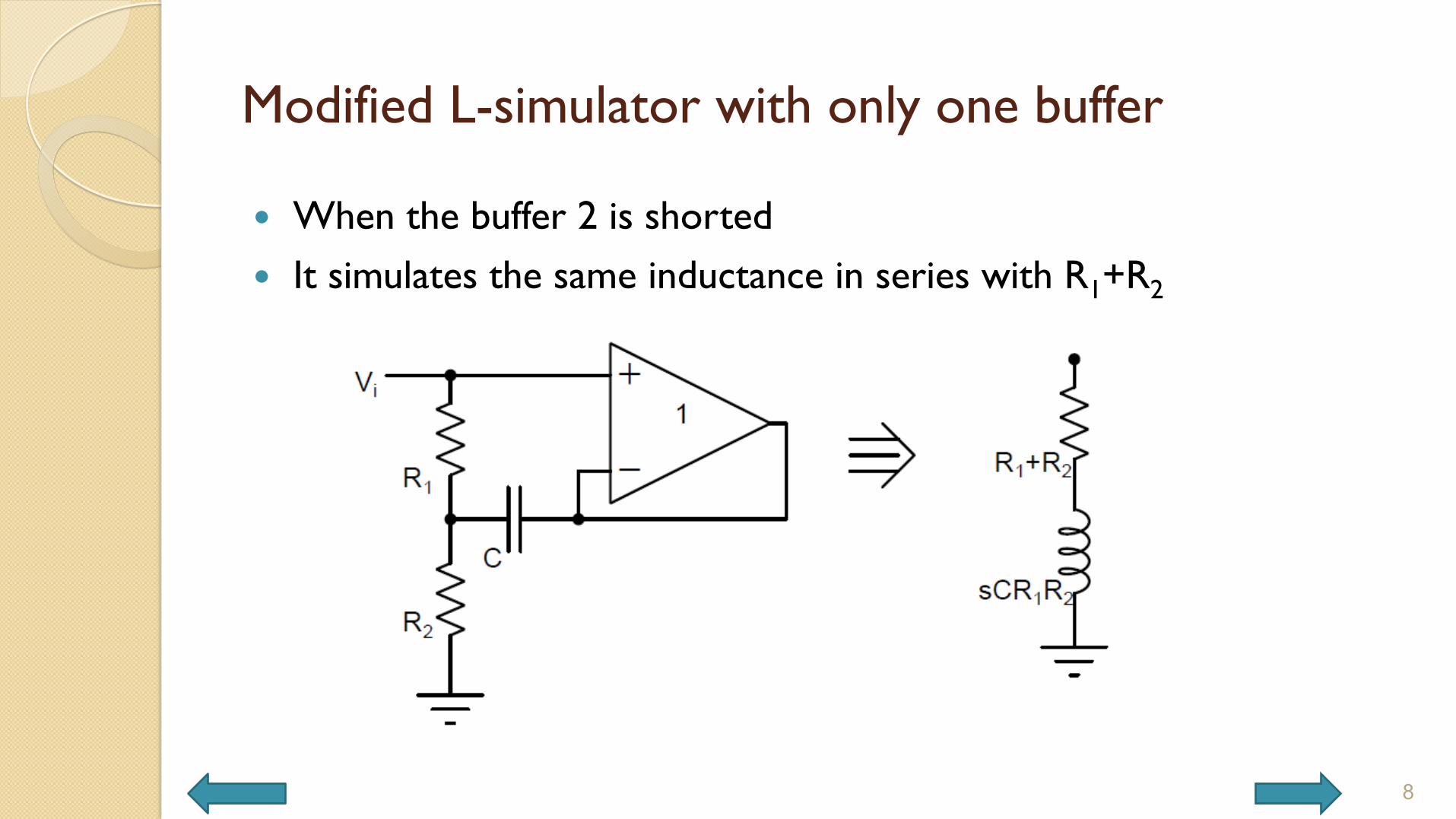
Modified L-simulator with only one buffer
� When the buffer 2 is shorted � It simulates the same inductance in series with R1+R2
8
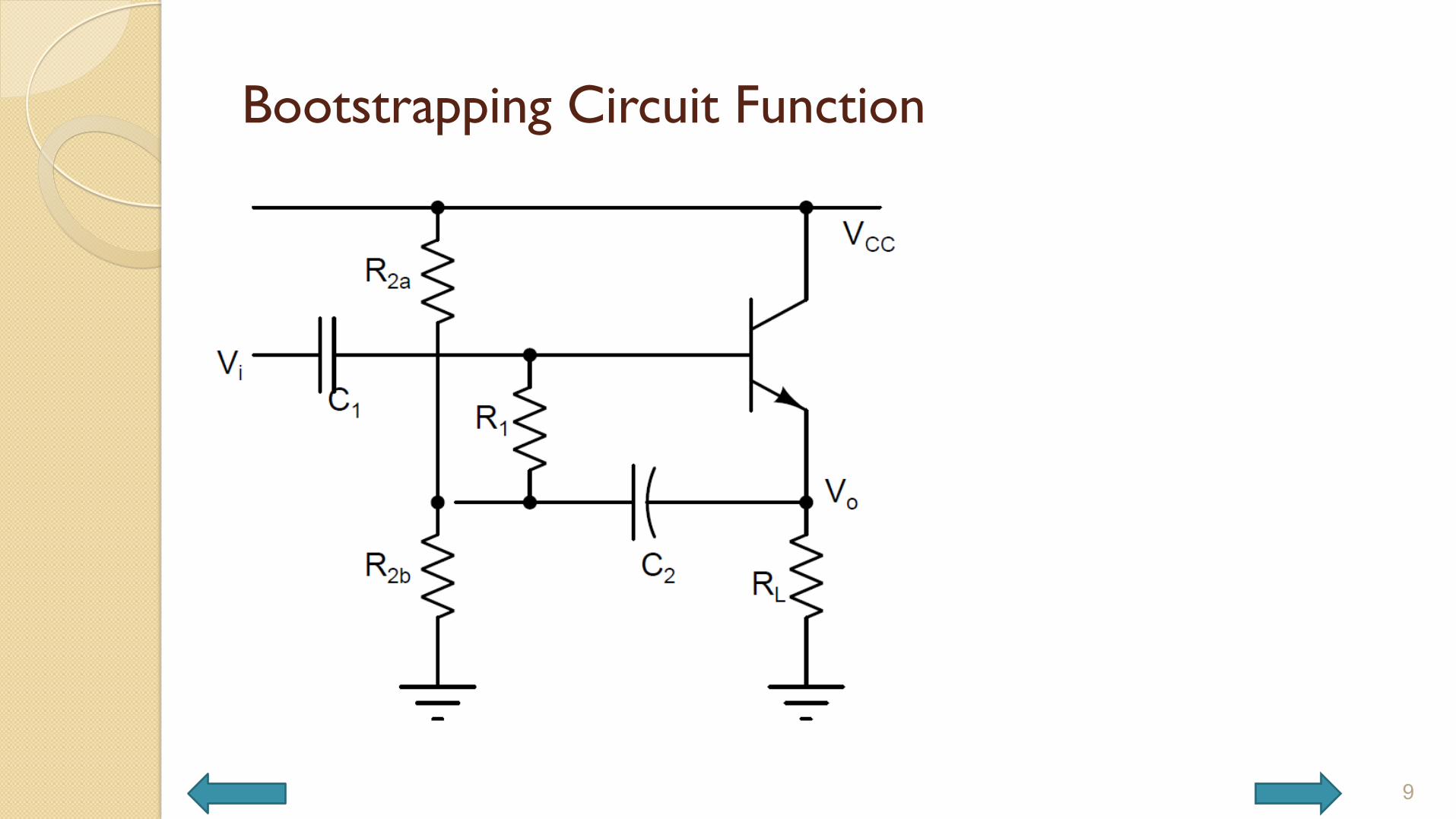
Bootstrapping Circuit Function
9
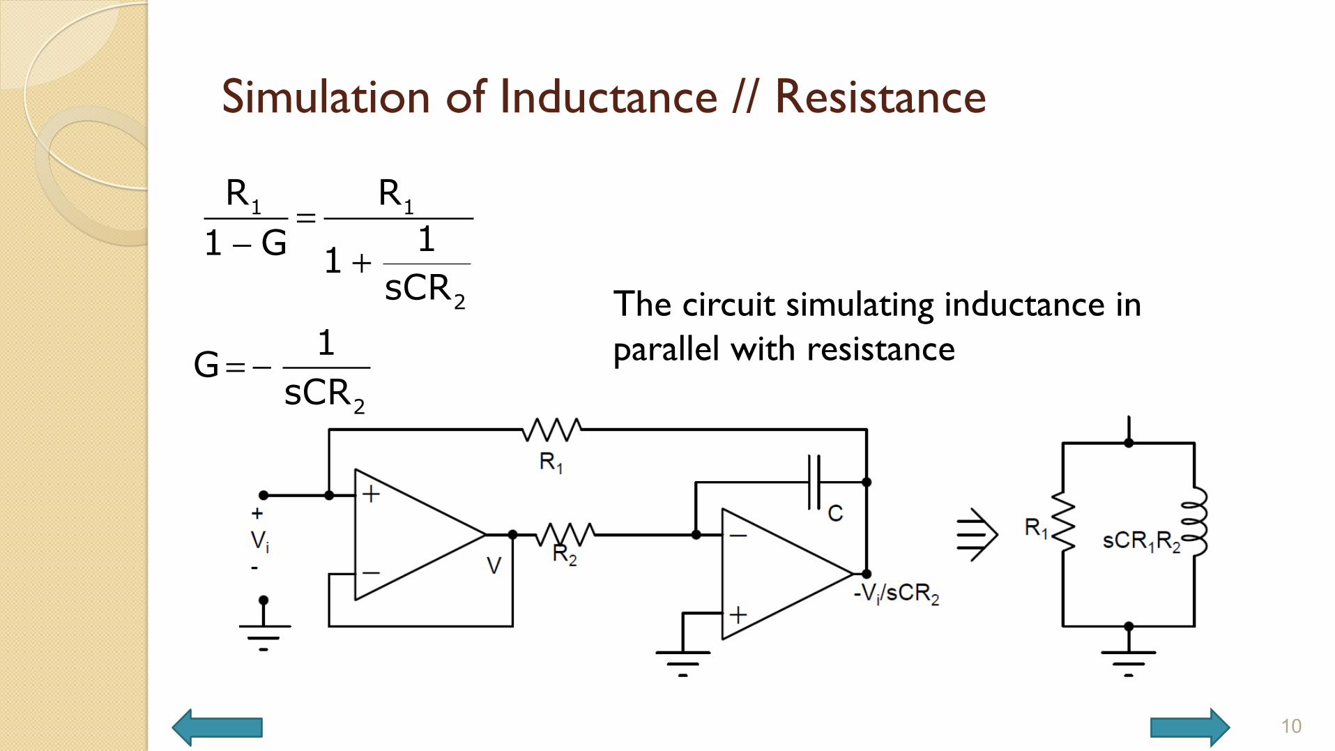
Simulation of Inductance // Resistance
10
1 1
2
2
R R11 G 1sCR
1GsCR
=− +
= −
The circuit simulating inductance in parallel with resistance
Simulation of Inductance // Resistance (contd.,)
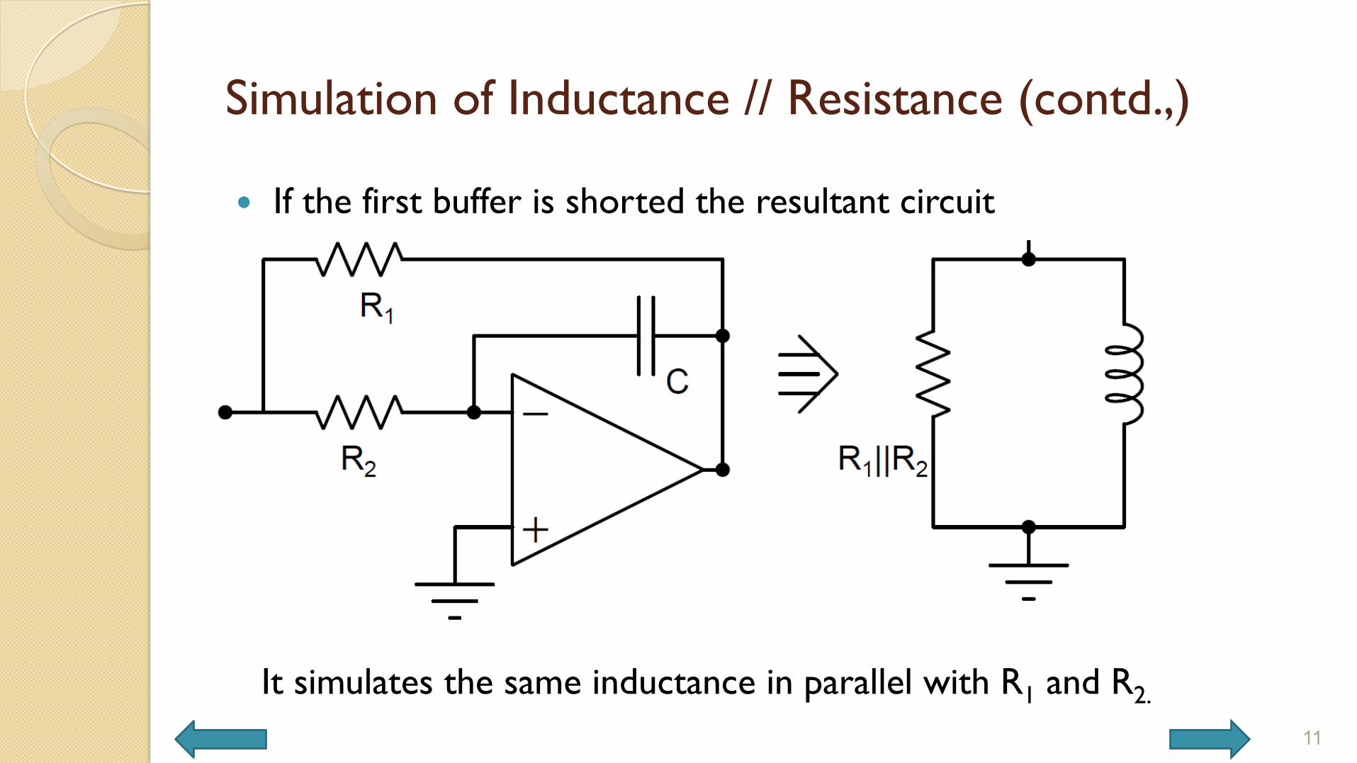
� If the first buffer is shorted the resultant circuit
11
It simulates the same inductance in parallel with R1 and R2.
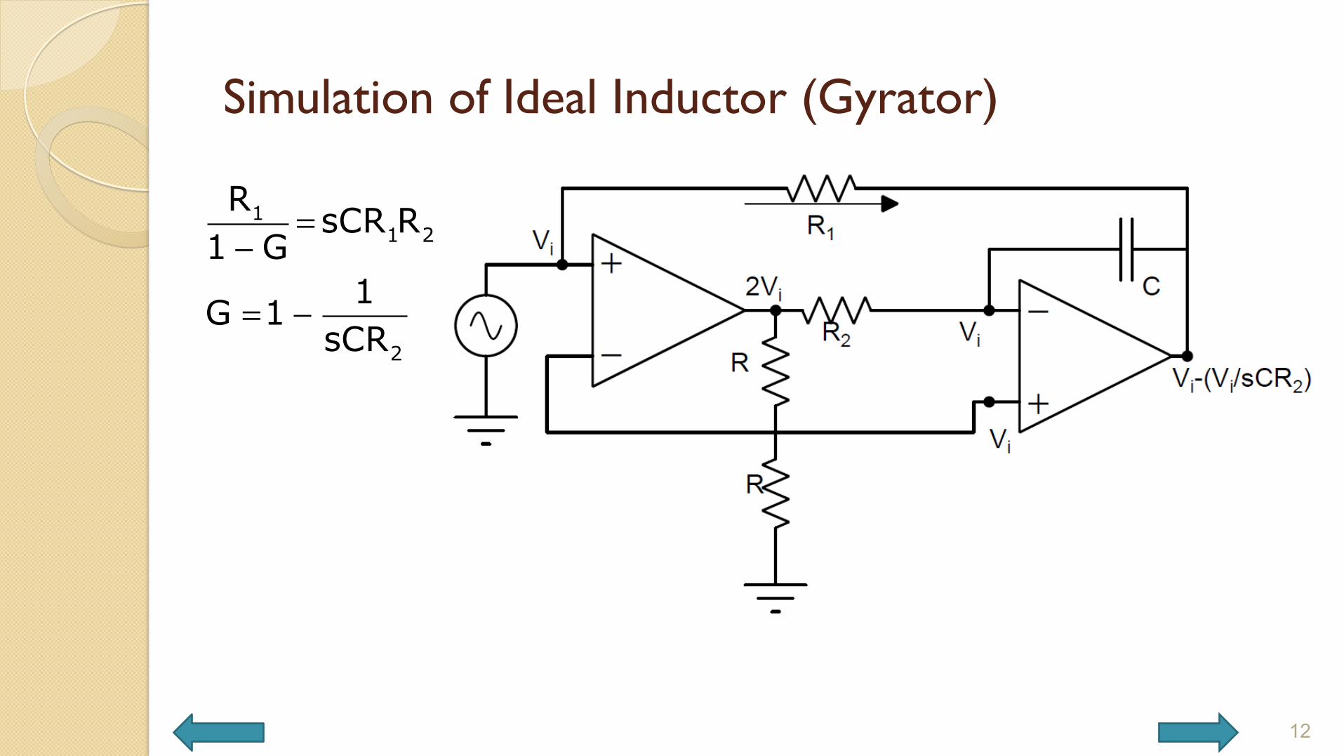
Simulation of Ideal Inductor (Gyrator)
12
11 2
2
R sCR R1 G
1G 1sCR
=−
= −
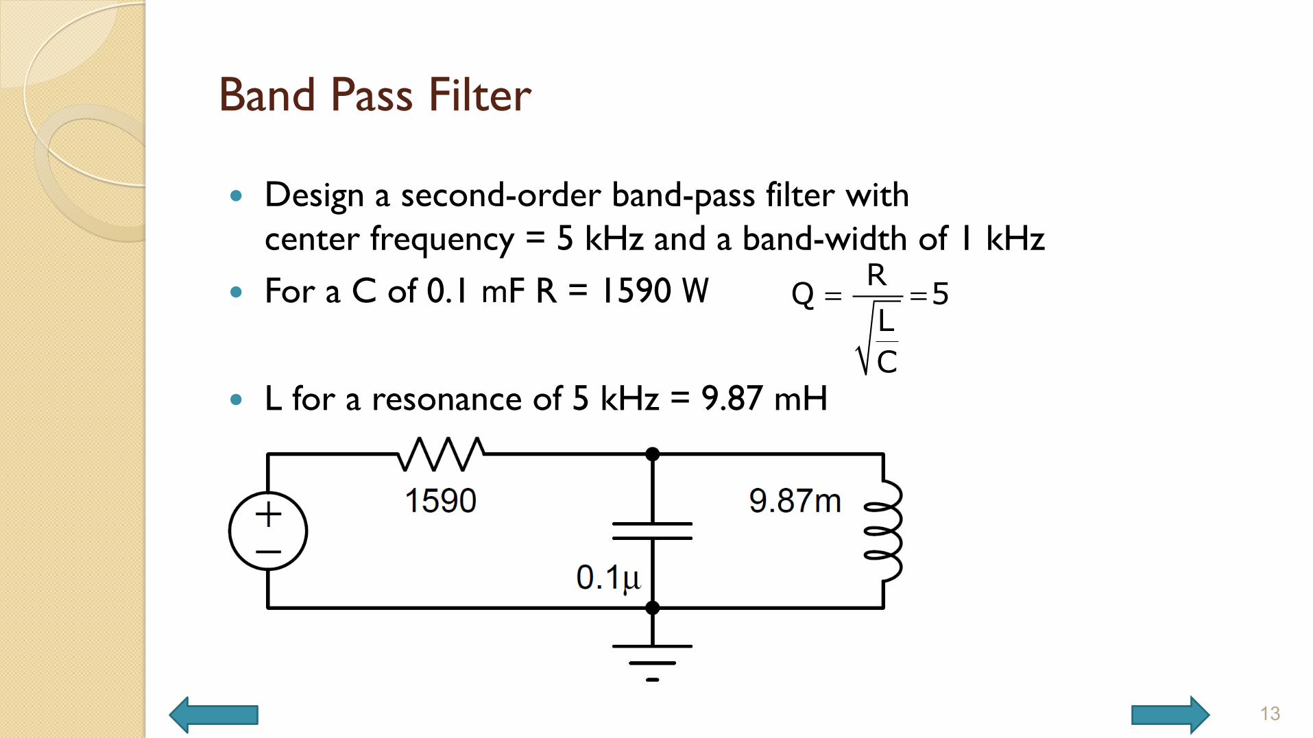
Band Pass Filter
� Design a second-order band-pass filter with center frequency = 5 kHz and a band-width of 1 kHz
� For a C of 0.1 mF R = 1590 W
� L for a resonance of 5 kHz = 9.87 mH
13
RQ 5LC
= =
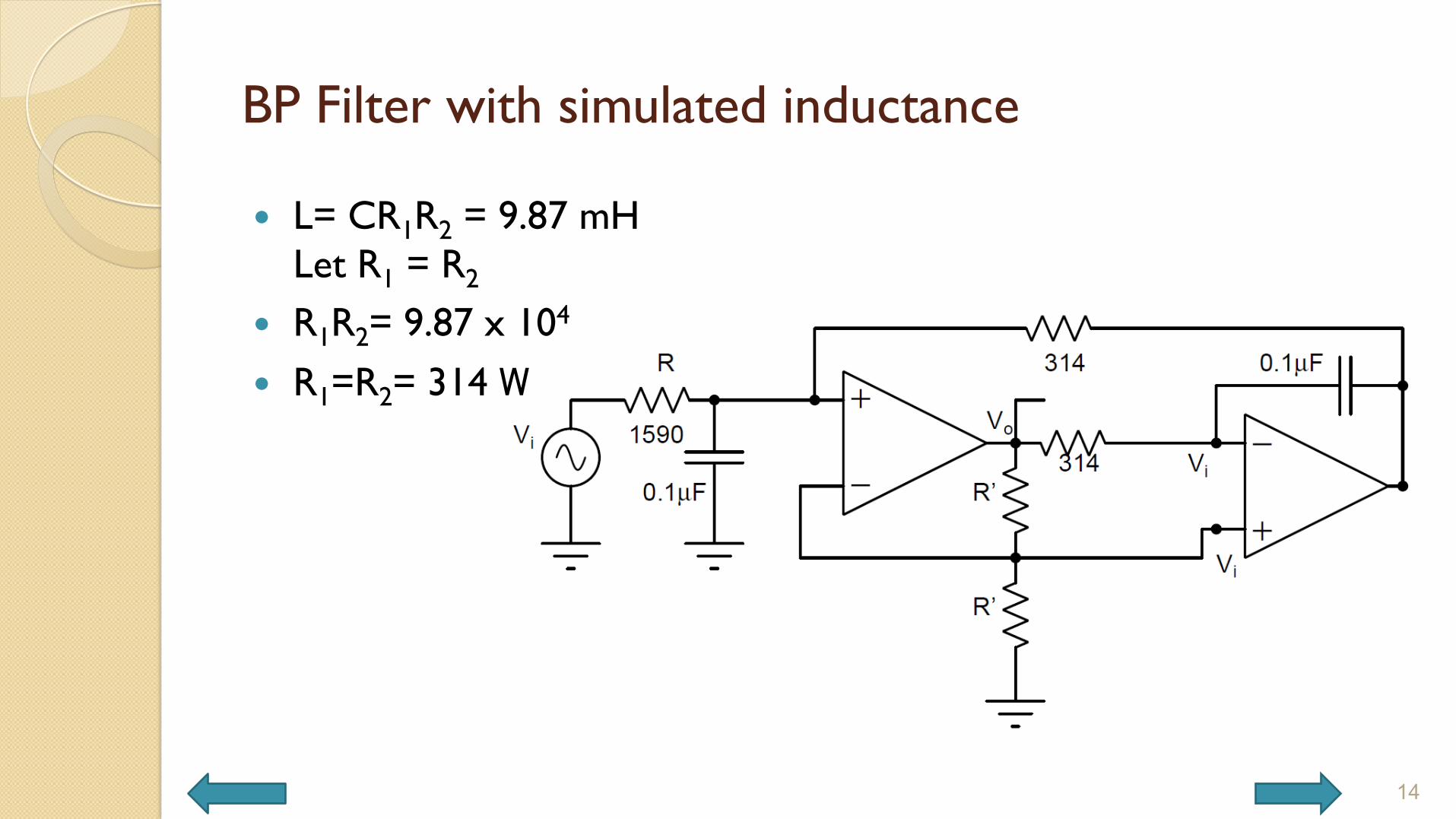
BP Filter with simulated inductance
� L= CR1R2 = 9.87 mH Let R1 = R2
� R1R2= 9.87 x 10⁴ � R1=R2= 314 W
14
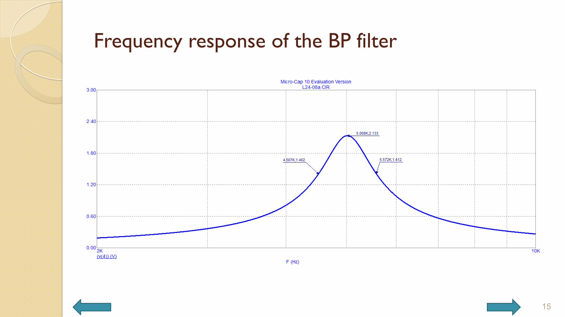
Frequency response of the BP filter
15
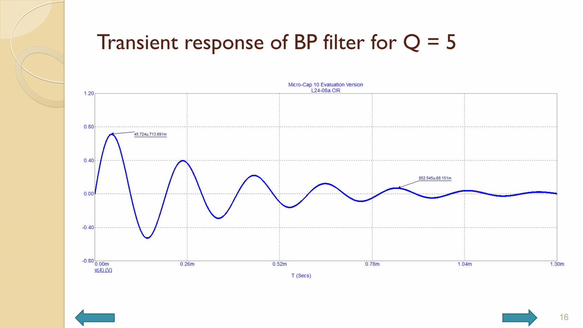
Transient response of BP filter for Q = 5
16
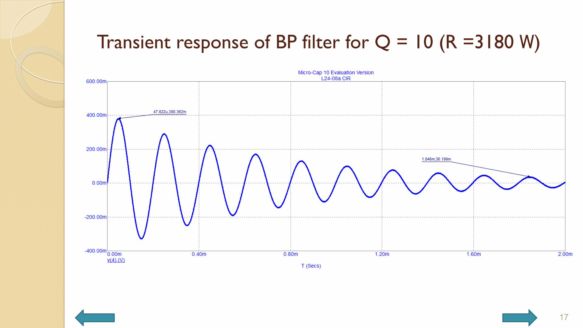
Transient response of BP filter for Q = 10 (R =3180 W)
17
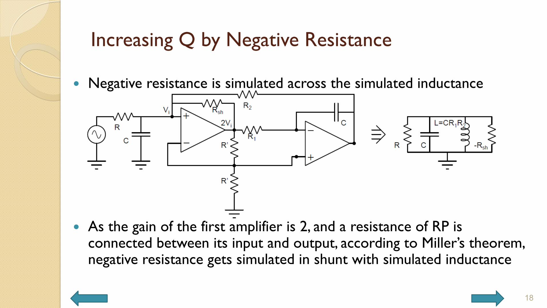
Increasing Q by Negative Resistance
� Negative resistance is simulated across the simulated inductance
� As the gain of the first amplifier is 2, and a resistance of RP is connected between its input and output, according to Miller’s theorem, negative resistance gets simulated in shunt with simulated inductance
18
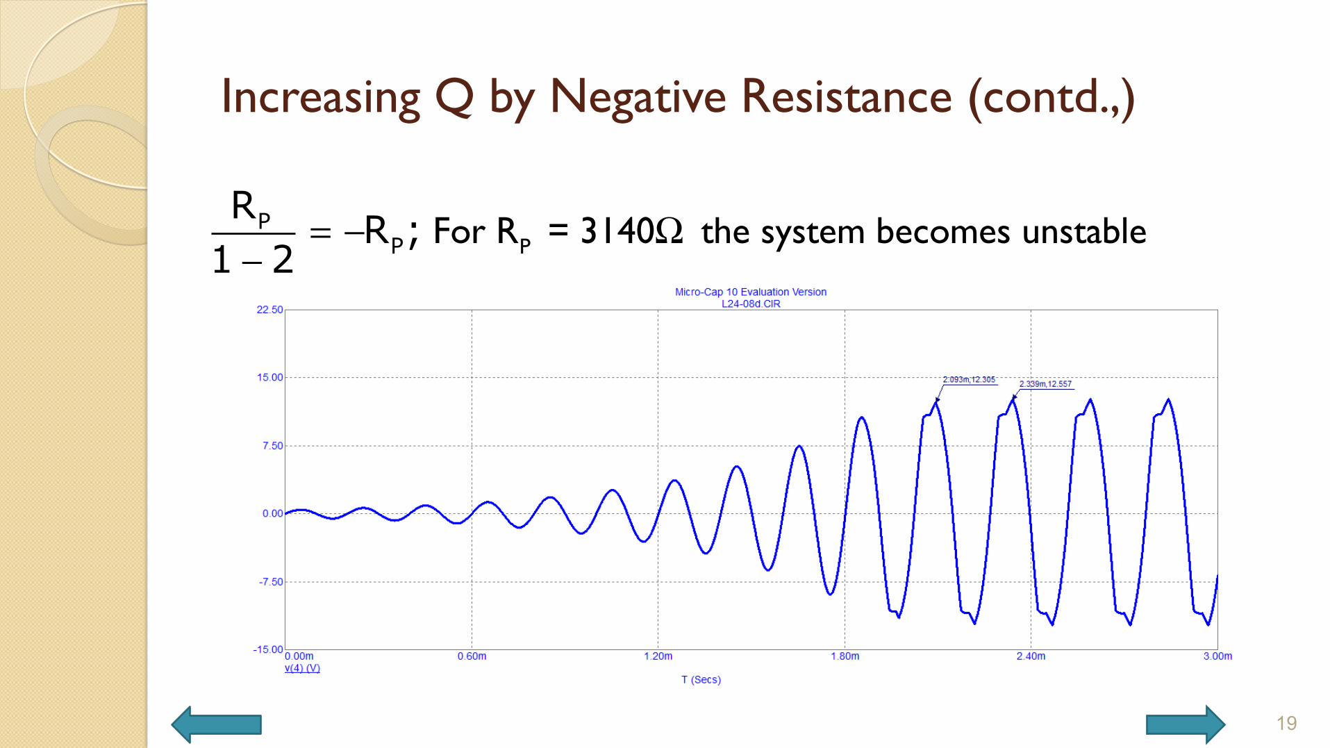
Increasing Q by Negative Resistance (contd.,)
19
PFor R = 3140 the system becomes unstablePP
R R ;1 2
= − Ω−
Increasing the resonant frequency
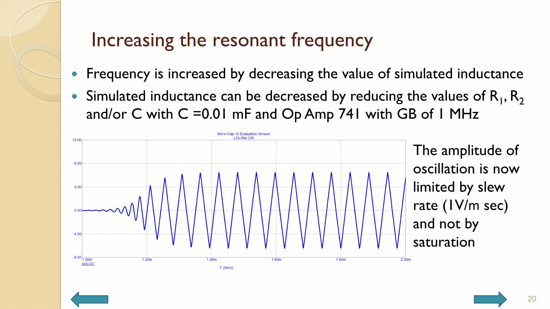
� Frequency is increased by decreasing the value of simulated inductance � Simulated inductance can be decreased by reducing the values of R1, R2
and/or C with C =0.01 mF and Op Amp 741 with GB of 1 MHz
20
The amplitude of oscillation is now limited by slew rate (1V/m sec) and not by saturation
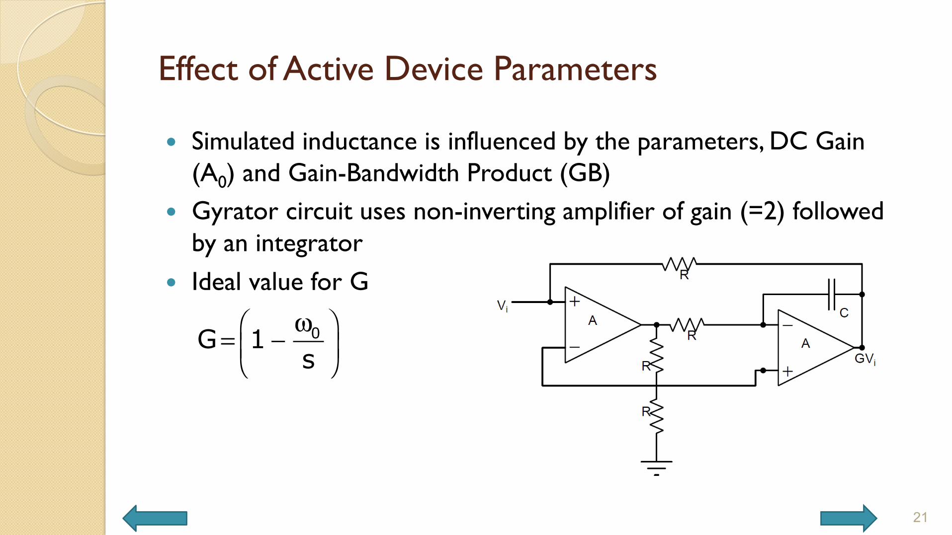
Effect of Active Device Parameters
� Simulated inductance is influenced by the parameters, DC Gain (A0) and Gain-Bandwidth Product (GB)
� Gyrator circuit uses non-inverting amplifier of gain (=2) followed by an integrator
� Ideal value for G
21
0G 1sω⎛ ⎞= −⎜ ⎟⎝ ⎠
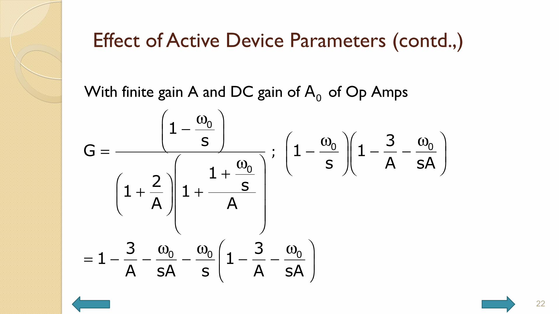
Effect of Active Device Parameters (contd.,)
22
With finite gain A and DC gain of of Op Amps0
0
0 0
0
0 0 0
A
1s 3G 1 1
s A sA12 s1 1A A
3 31 1A sA s A sA
ω⎛ ⎞−⎜ ⎟ ω ω⎛ ⎞ ⎛ ⎞⎝ ⎠= − − −⎜ ⎟ ⎜ ⎟ω⎛ ⎞ ⎝ ⎠ ⎝ ⎠+⎜ ⎟⎛ ⎞+ +⎜ ⎟⎜ ⎟⎝ ⎠ ⎜ ⎟⎜ ⎟⎝ ⎠ω ω ω⎛ ⎞= − − − − −⎜ ⎟
⎝ ⎠
;
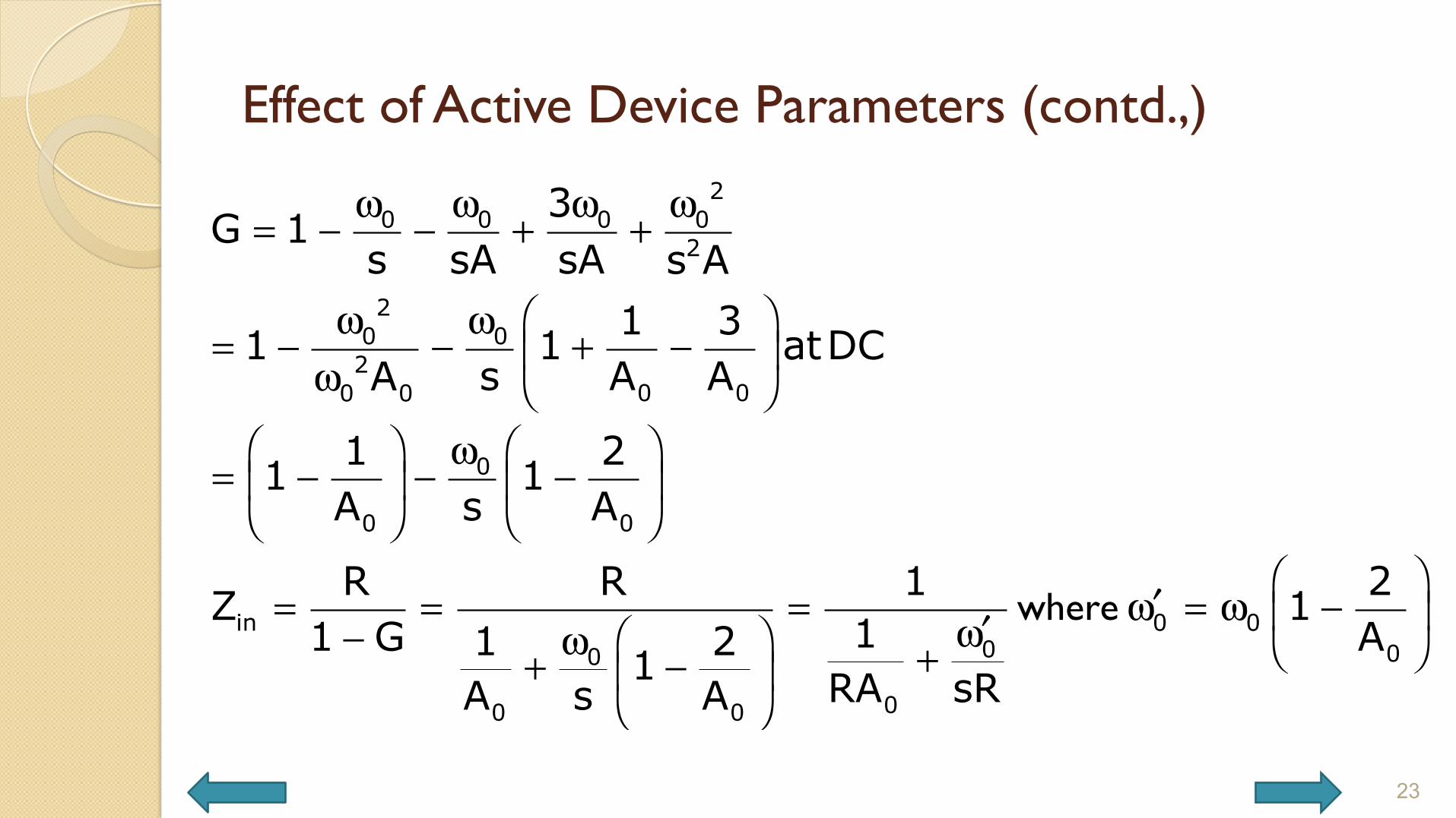
Effect of Active Device Parameters (contd.,)
23
where
20 0 0 0
2
20 02
0 00 0
0
0 0
in 0 00 00
00 0
3G 1s sA sA s A
1 31 1 atDCs A AA
1 21 1A s A
R R 1 2Z 111 G A1 21 RA sRA s A
ω ω ω ω= − − + +
⎛ ⎞ω ω= − − + −⎜ ⎟ω ⎝ ⎠⎛ ⎞ ⎛ ⎞ω
= − − −⎜ ⎟ ⎜ ⎟⎝ ⎠ ⎝ ⎠
⎛ ⎞′= = = ω = ω −⎜ ⎟′ω− ⎛ ⎞ω ⎝ ⎠++ −⎜ ⎟
⎝ ⎠
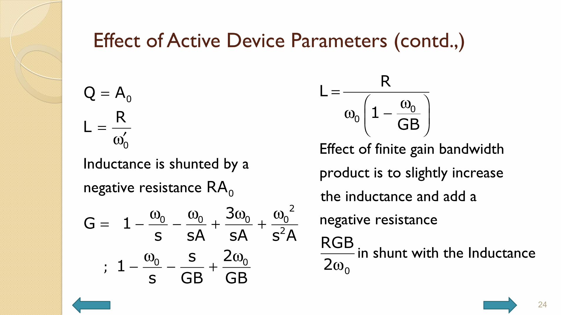
Effect of Active Device Parameters (contd.,)
24
Inductance is shunted by a
negative resistance
0
0
02
0 0 0 02
0 0
Q ARL
RA
3G 1s sA sA s A
2s1s GB GB
=
=′ω
ω ω ω ω= − − + +
ω ω− − +;
Effect of finite gain bandwidth
product is to slightly increase
the inductance and add a negative resistance
in shunt with the Inductance
00
0
RL1GB
RGB2
=ω⎛ ⎞ω −⎜ ⎟⎝ ⎠
ω
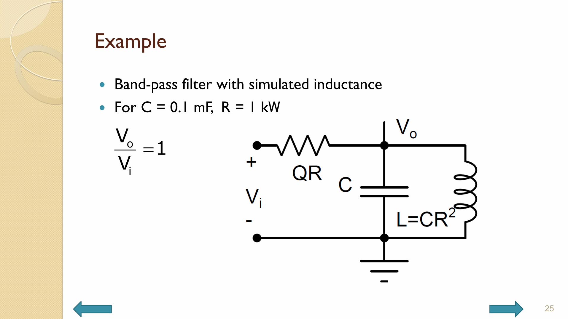
Example
� Band-pass filter with simulated inductance � For C = 0.1 mF, R = 1 kW
25
=o
i
V 1V
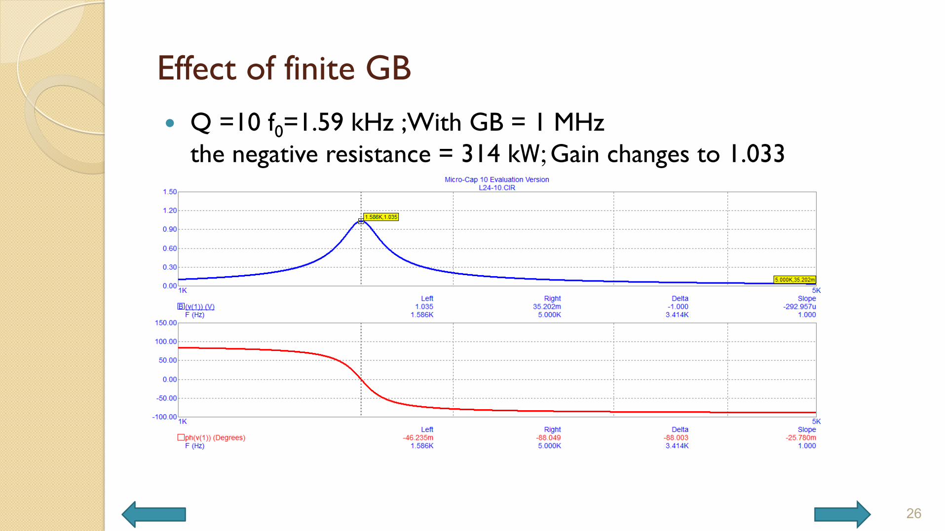
Effect of finite GB � Q =10 f0=1.59 kHz ;With GB = 1 MHz
the negative resistance = 314 kW; Gain changes to 1.033
26
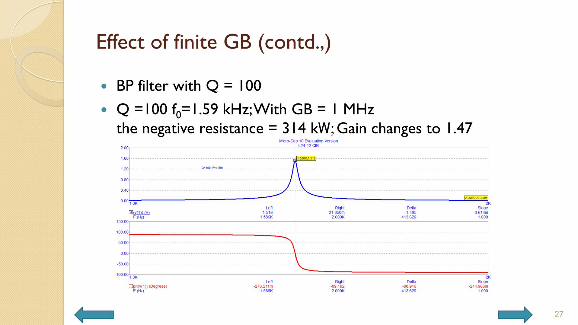
Effect of finite GB (contd.,)
� BP filter with Q = 100 � Q =100 f0=1.59 kHz; With GB = 1 MHz
the negative resistance = 314 kW; Gain changes to 1.47
27
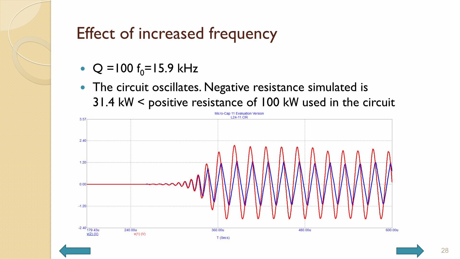
Effect of increased frequency
� Q =100 f0=15.9 kHz � The circuit oscillates. Negative resistance simulated is
31.4 kW < positive resistance of 100 kW used in the circuit
28
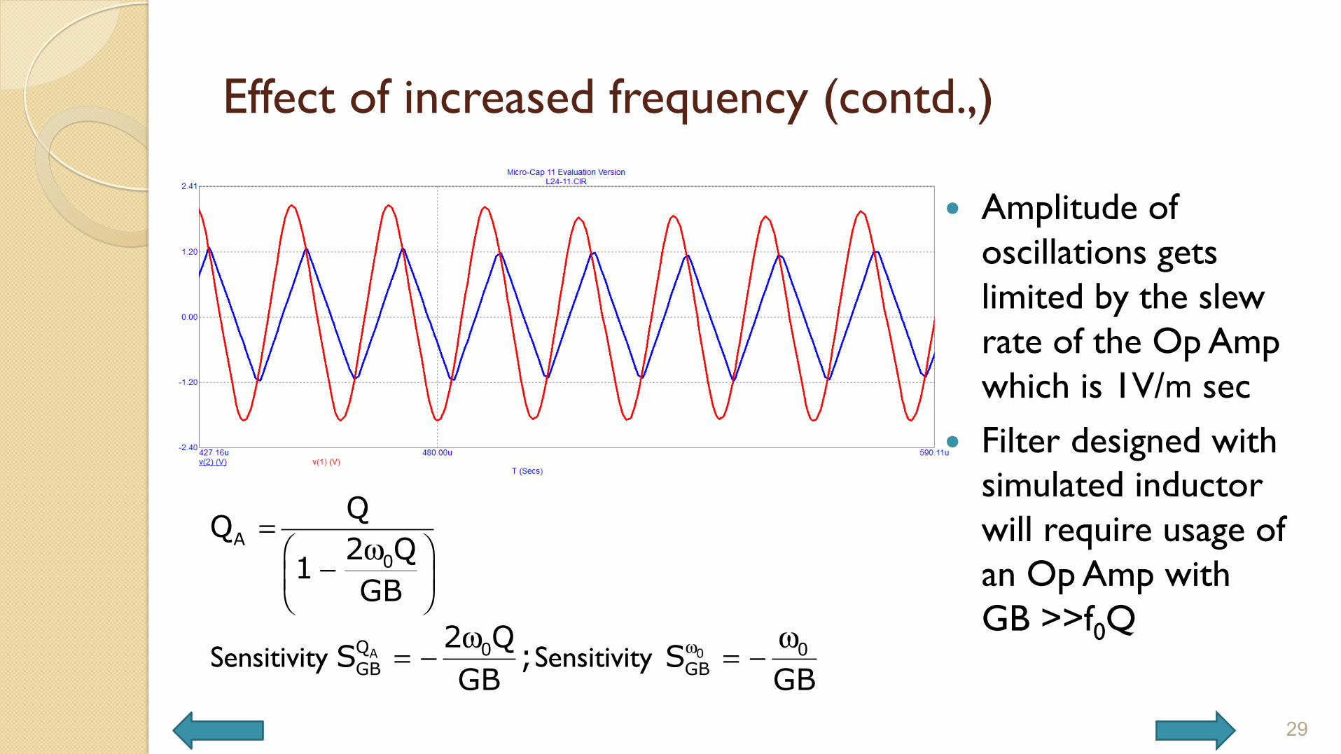
Effect of increased frequency (contd.,)
� Amplitude of oscillations gets limited by the slew rate of the Op Amp which is 1V/m sec
� Filter designed with simulated inductor will require usage of an Op Amp with GB >>f0Q
29
Sensitivity Sensitivity 0A
A0
Q 0 0GB GB
QQ2 Q1GB
2 QS ; SGB GB
ω
=ω⎛ ⎞−⎜ ⎟⎝ ⎠
ω ω= − = −
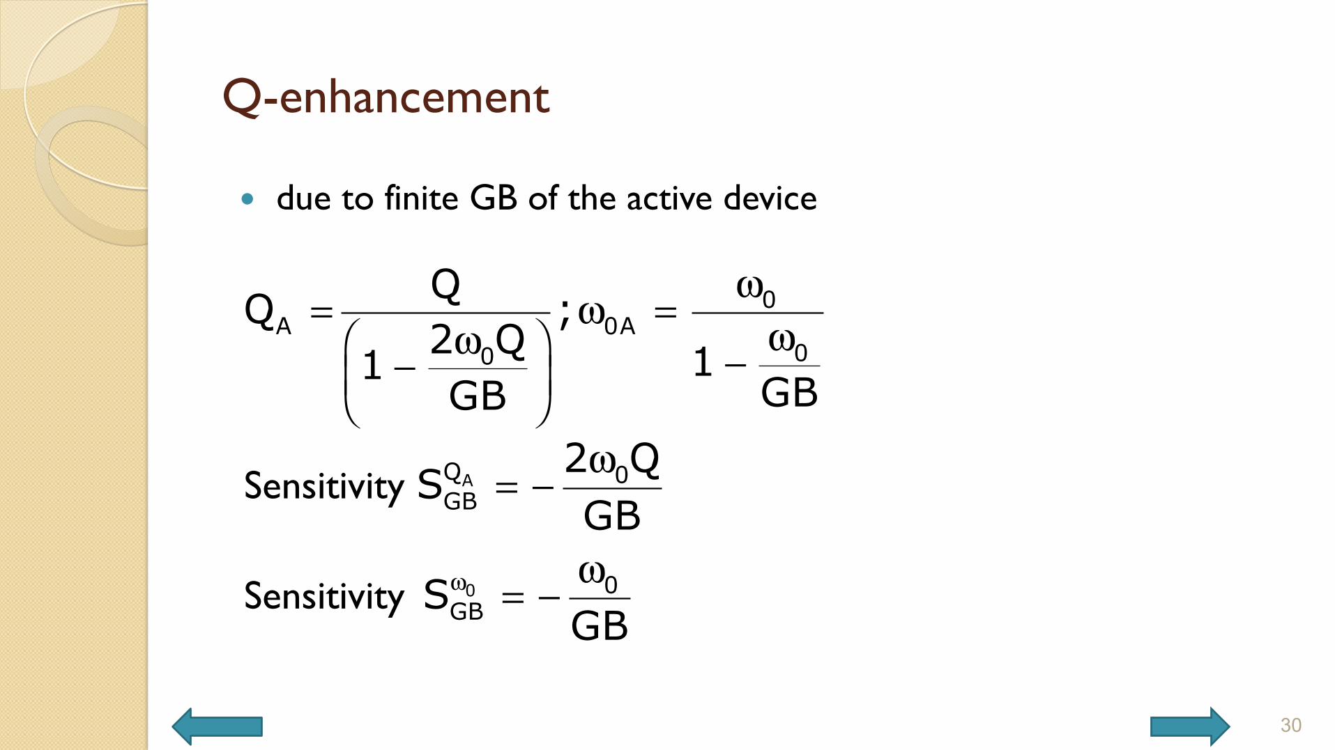
Q-enhancement
� due to finite GB of the active device
30
Sensitivity
Sensitivity
A
0
0A 0A
00
Q 0GB
0GB
QQ ;2 Q 11
GBGB2 QSGB
SGB
ω
ω= ω =
ωω⎛ ⎞ −−⎜ ⎟⎝ ⎠ω
= −
ω= −
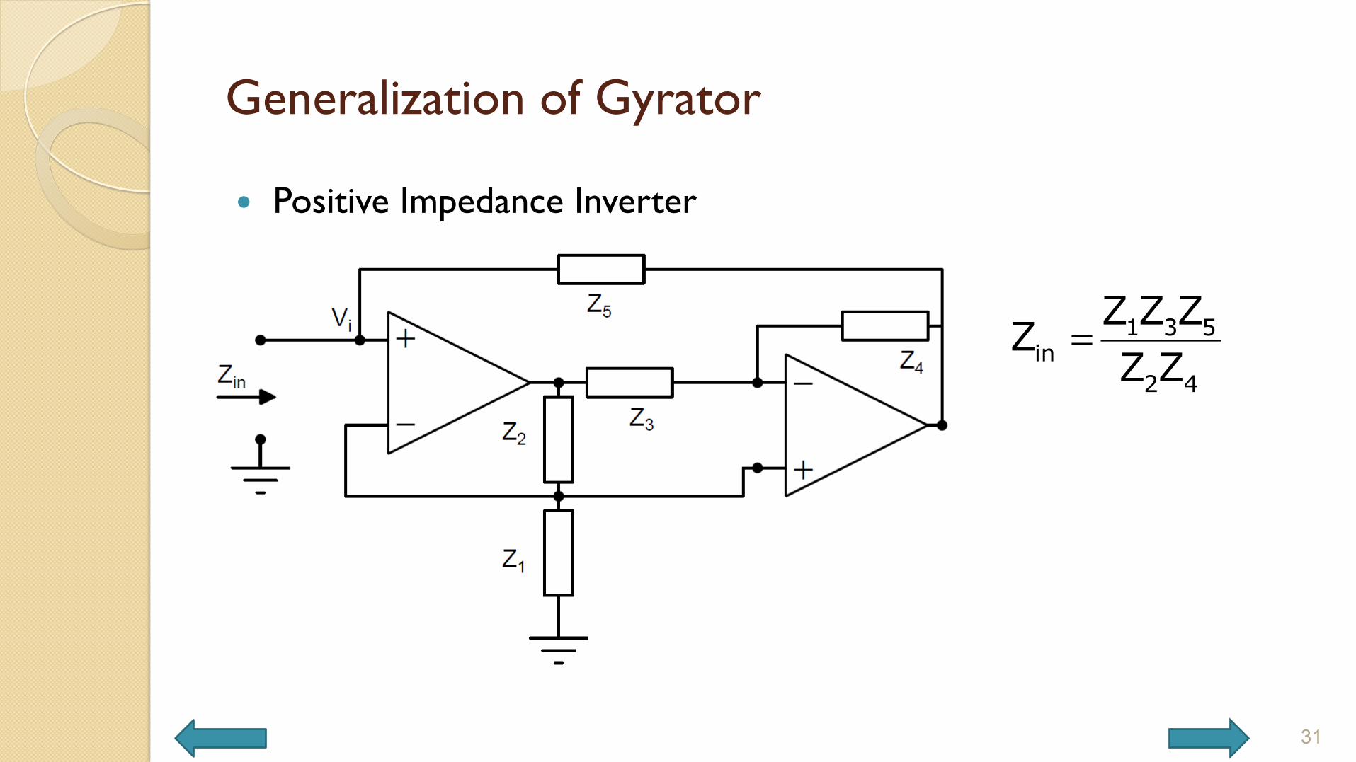
Generalization of Gyrator
� Positive Impedance Inverter
31
1 3 5in
2 4
Z Z ZZZ Z
=
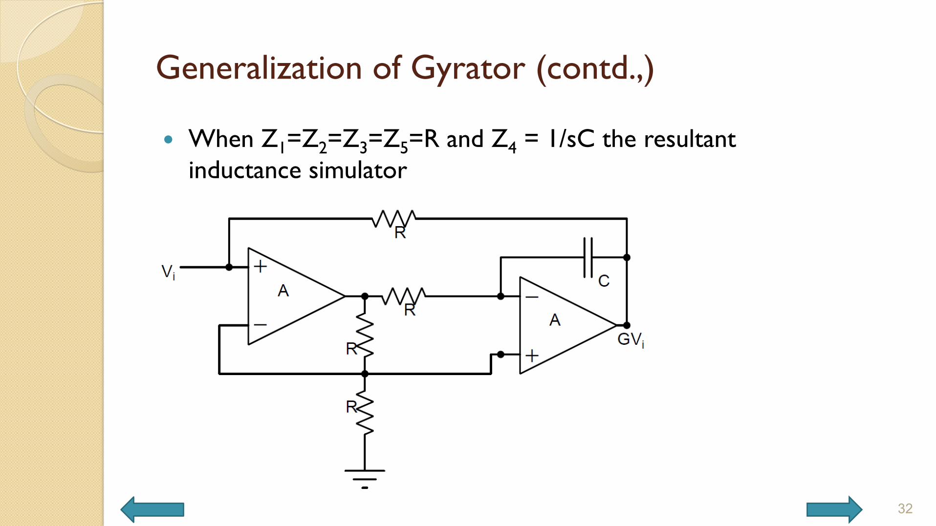
Generalization of Gyrator (contd.,)
� When Z1=Z2=Z3=Z5=R and Z4 = 1/sC the resultant inductance simulator
32
Generalization of Gyrator (contd.,)
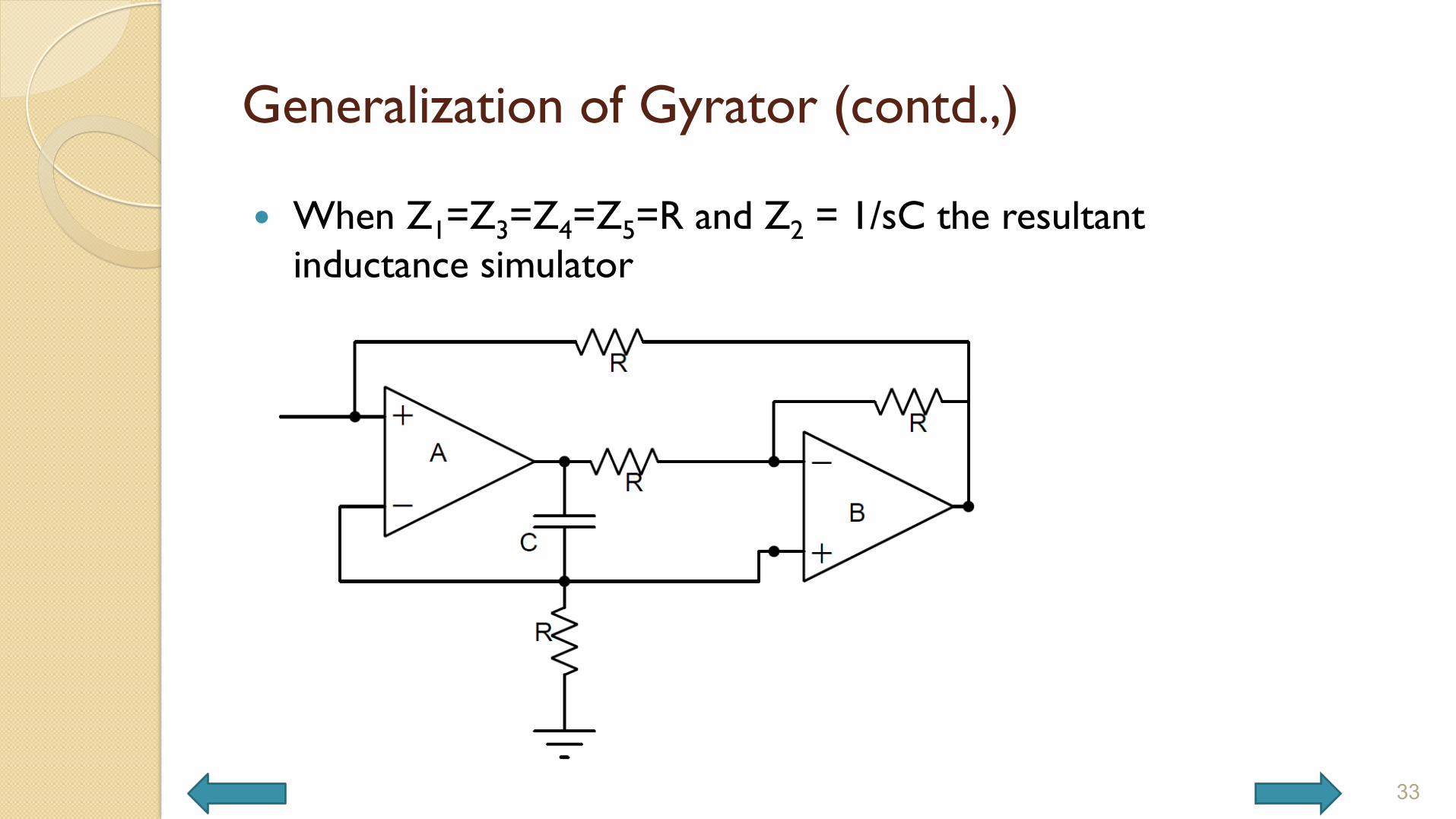
� When Z1=Z3=Z4=Z5=R and Z2 = 1/sC the resultant inductance simulator
33
Conclusion
34