Embed Size (px)
Citation preview

Analog to Digital Converters (ADC)
2
©Paul GodinCreated April 2008
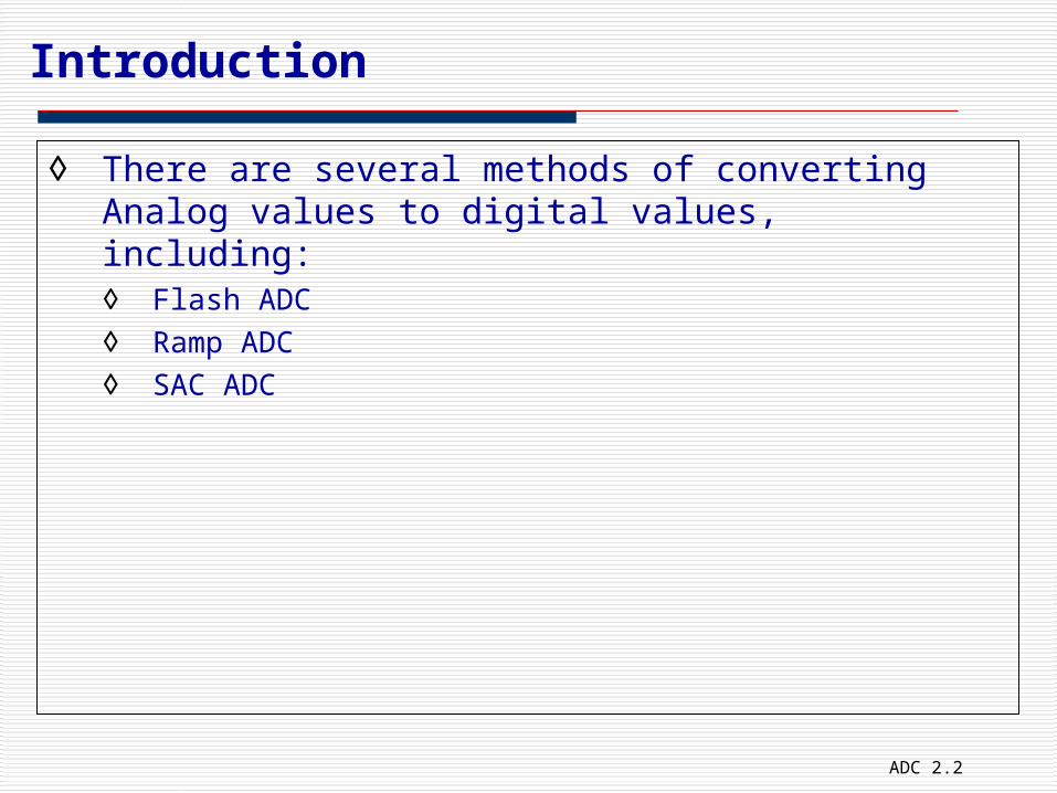
Introduction
◊ There are several methods of converting Analog values to digital values, including:◊ Flash ADC◊ Ramp ADC◊ SAC ADC
ADC 2.2

Other Methods of ADC
◊ Up/Down Ramp◊ Similar to the Ramp ADC but instead of starting the count
at zero for each measurement it increments the counter up or down based on the direction of the analog input. The time it takes for conversion is variable.
◊ Voltage-Frequency ADC◊ This device utilizes a Voltage Controlled Oscillator (VCO).
The higher the input voltage the higher the output frequency of the VCO. The ADC enables the output of the VCO for a specific period of time and the output of the oscillator is connected to a counter. The result of the count is supplied as the digital value.
ADC 2.3

Other Methods of ADC
◊ Sigma/Delta◊ Creates an internal bitstream based upon the difference
(Delta) between the analog input and a feedback comparator. The running total (Sigma) is reported as the digitized value. Operates at a high internal frequency.
See http://www.analog.com/Analog_Root/static/techSupport/designTools/interactiveTools/sdtutorial/sdtutorial.html for more information.
ADC 2.4

Errors
◊ Analog to Digital systems have several possible sources of error.
◊ The errors can be the result of:◊ Quantization◊ Noise◊ Slew◊ Under-Sampling
ADC 2.5

Quantization Error
◊ Quantization errors are a normal occurrence for ADCs. The input voltage will commonly have a value that is between the LSB voltage step and must be rounded up or down.
◊ For instance, if the resolution is 20mV per bit and a value of 10 mV is applied, the ADC will interpret this as either 0v or 20 mV, depending on the ADC design.
ADC 2.6

Quantization
◊ There are several additional quantization issues:
◊ If the total number of bits representing the amplitude of the signal is too small the quantization error increases.
◊ If the voltage applied to the ADC is not properly compensated then the full range of output values is not used.
ADC 2.7

Quantization and Sampling
◊ Sampling-Related Quantization Errors
◊ Relatively low sampling frequencies can lead to quantization errors
◊ If the sampling frequency is slightly different from the analog signal’s frequency (or a harmonic..a factor of the frequency), then the values may not indicate all the peaks and valleys, leading to other harmonics (also see aliasing).
ADC 2.8

Not quite perfect...lower sample rate
Above: original signal with samplesBelow: imperfections in the digital output quantization
ADC 2.9
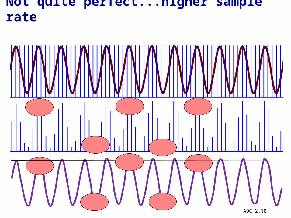
Not quite perfect...higher sample rate
ADC 2.10
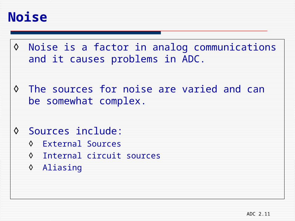
Noise
◊ Noise is a factor in analog communications and it causes problems in ADC.
◊ The sources for noise are varied and can be somewhat complex.
◊ Sources include:◊ External Sources◊ Internal circuit sources◊ Aliasing
ADC 2.11

Aliasing
◊ Higher quality ADC (and DAC) will contain anti-aliasing filters to remove frequencies that are aliasing (“posing”) as signal.
◊ Aliasing occurs when additional frequencies are inadvertently produced in the AD process.
◊ For instance, if there are some frequencies present in the original signal that are higher than the Nyquist sample rate, a different lower frequency may appear on the conversion.
◊ Aliasing also occurs with adequate sampling frequencies.
ADC 2.12

Aliasing with Inadequate Sampling Rate
ADC 2.13

Aliasing with an Adequate Sampling Rate
ADC 2.14

Noise Sources
◊ Analog values are susceptible to noise (an advantage of digital electronics!). This noise causes problems for the AD conversion, as the noise will be included in the conversion process.
◊ There are external and internal sources of noise.◊ External: use filters and proper techniques to minimize
noise (such as decoupling, isolation, etc)◊ Internal: switching noise occurs with AD converters. Use
filters, decoupling and ground isolation. Thermal noise (aka white noise) is caused by a variety of reasons.◊ Other solutions include processing the signal (DSP),
injecting additional white noise to help average out the noise and ignoring the LSB.
ADC 2.15

Filter
◊ The analog input to an ADC should contain a low-pass filter to ensure high frequencies cannot pass and create aliasing problems.
◊ Advanced filtering techniques are also employed. These include DSP (Digital Signal Processing) to mathematically analyze and adjust the digital values.
ADC 2.16
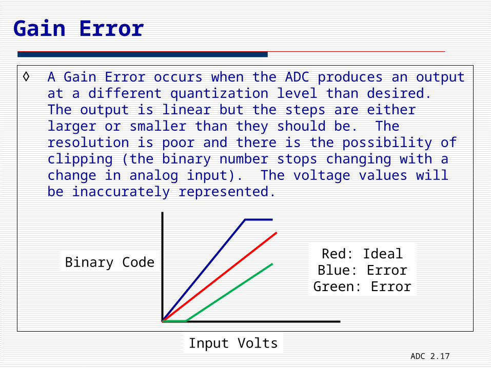
Gain Error
◊ A Gain Error occurs when the ADC produces an output at a different quantization level than desired. The output is linear but the steps are either larger or smaller than they should be. The resolution is poor and there is the possibility of clipping (the binary number stops changing with a change in analog input). The voltage values will be inaccurately represented.
Red: IdealBlue: Error
Green: Error
Input Volts
Binary Code
ADC 2.17

Gain Error
Red: IdealBlue: Error
Green: Error
Typical Causes: •wrong VDD/VEE/Vreference voltage to the ADC•Improper Analog input voltage
ADC 2.18

Offset Error
◊ An Offset Error occurs when the output has the same voltage per step but the starting voltage is different.
Red: IdealBlue: Error
Green: Error
Input Volts
Binary Code
ADC 2.19

Offset Error
Red: IdealBlue: Error
Green: Error
Typical Causes: •Improper ground reference•Improper analog voltage range
ADC 2.20

Non-Linearity: Non-Monotonic
◊ A Monotonic Error occurs when the individual voltage steps are non-linear.
Red: IdealBlue: Error
Input Volts
Binary Code
ADC 2.21

Non-Linearity: Non-Monotonic
Red: IdealBlue: Error
Typical Causes: •defective ADC•wrong outputs measured•significant noise on ac input
ADC 2.22

Slew
◊ Slew represents the maximum rate of change of a signal. Slew rate is measured in V/t.
Black: ideal binary step from ADCGrey: binary step from ADC with slew
ADC 2.23
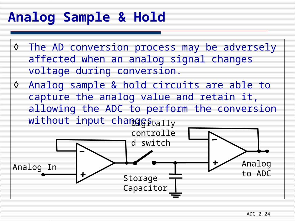
Analog Sample & Hold
◊ The AD conversion process may be adversely affected when an analog signal changes voltage during conversion.
◊ Analog sample & hold circuits are able to capture the analog value and retain it, allowing the ADC to perform the conversion without input changes.
ADC 2.24
Analog In
Digitally controlled switch
StorageCapacitor
Analogto ADC

Specification Sheet
◊ View the specification sheet for the ADC08 from National Instruments.
◊ Definitions: ◊ Common-Mode noise is noise that occurs on both
conductors at the same time.◊ Ratiometric means measures the ratio, or takes ratio into
account when measuring.
ADC 2.25

DSP
◊ Digital Signal Processors perform operations on the digitized signals including:◊ removing interference, noise and other frequency and
transmission effects◊ encoding the values for transmission◊ reconstruct signals by enhancing or decreasing specific
frequencies
◊ DSPs are complex devices that rely on programming code (algorithms) to perform operations.
ADC 2.26

ADC-DAC with DSP
FilterFilter ADCADC DSPDSP
DACDACDSPDSP FilterFilter
ADC 2.27

DSP
◊ Analog signals contain noise. Noise can be filtered but sometimes the filtering process can eliminate wanted frequencies.
◊ The better means of removing noise is to take an average, as illustrated below as the red line.
Analog Signal with Noise
ADC 2.28

DSP (a simplified representation)
ADC Registers with samples
Registers with older samples
Multiplier
Cumulativeadder
ADC 2.29

©Paul R. Godinprgodin°@ gmail.com
END ADC2
ADC 2.30