Embed Size (px)
Citation preview
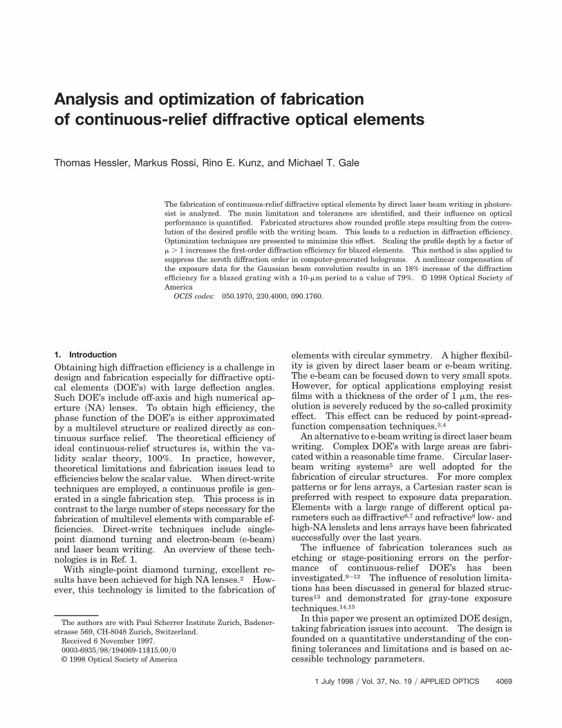
Analysis and optimization of fabricationof continuous-relief diffractive optical elements
Thomas Hessler, Markus Rossi, Rino E. Kunz, and Michael T. Gale
The fabrication of continuous-relief diffractive optical elements by direct laser beam writing in photore-sist is analyzed. The main limitation and tolerances are identified, and their influence on opticalperformance is quantified. Fabricated structures show rounded profile steps resulting from the convo-lution of the desired profile with the writing beam. This leads to a reduction in diffraction efficiency.Optimization techniques are presented to minimize this effect. Scaling the profile depth by a factor ofm . 1 increases the first-order diffraction efficiency for blazed elements. This method is also applied tosuppress the zeroth diffraction order in computer-generated holograms. A nonlinear compensation ofthe exposure data for the Gaussian beam convolution results in an 18% increase of the diffractionefficiency for a blazed grating with a 10-mm period to a value of 79%. © 1998 Optical Society ofAmerica
OCIS codes: 050.1970, 230.4000, 090.1760.
1. Introduction
Obtaining high diffraction efficiency is a challenge indesign and fabrication especially for diffractive opti-cal elements ~DOE’s! with large deflection angles.Such DOE’s include off-axis and high numerical ap-erture ~NA! lenses. To obtain high efficiency, thephase function of the DOE’s is either approximatedby a multilevel structure or realized directly as con-tinuous surface relief. The theoretical efficiency ofideal continuous-relief structures is, within the va-lidity scalar theory, 100%. In practice, however,theoretical limitations and fabrication issues lead toefficiencies below the scalar value. When direct-writetechniques are employed, a continuous profile is gen-erated in a single fabrication step. This process is incontrast to the large number of steps necessary for thefabrication of multilevel elements with comparable ef-ficiencies. Direct-write techniques include single-point diamond turning and electron-beam ~e-beam!and laser beam writing. An overview of these tech-nologies is in Ref. 1.
With single-point diamond turning, excellent re-sults have been achieved for high NA lenses.2 How-ever, this technology is limited to the fabrication of
The authors are with Paul Scherrer Institute Zurich, Badener-strasse 569, CH-8048 Zurich, Switzerland.
Received 6 November 1997.0003-6935y98y194069-11$15.00y0© 1998 Optical Society of America
elements with circular symmetry. A higher flexibil-ity is given by direct laser beam or e-beam writing.The e-beam can be focused down to very small spots.However, for optical applications employing resistfilms with a thickness of the order of 1 mm, the res-olution is severely reduced by the so-called proximityeffect. This effect can be reduced by point-spread-function compensation techniques.3,4
An alternative to e-beam writing is direct laser beamwriting. Complex DOE’s with large areas are fabri-cated within a reasonable time frame. Circular laser-beam writing systems5 are well adopted for thefabrication of circular structures. For more complexpatterns or for lens arrays, a Cartesian raster scan ispreferred with respect to exposure data preparation.Elements with a large range of different optical pa-rameters such as diffractive6,7 and refractive8 low- andhigh-NA lenslets and lens arrays have been fabricatedsuccessfully over the last years.
The influence of fabrication tolerances such asetching or stage-positioning errors on the perfor-mance of continuous-relief DOE’s has beeninvestigated.9–12 The influence of resolution limita-tions has been discussed in general for blazed struc-tures13 and demonstrated for gray-tone exposuretechniques.14,15
In this paper we present an optimized DOE design,taking fabrication issues into account. The design isfounded on a quantitative understanding of the con-fining tolerances and limitations and is based on ac-cessible technology parameters.
1 July 1998 y Vol. 37, No. 19 y APPLIED OPTICS 4069
The underlying design and modeling methods forcontinuous-relief DOE’s are described in Section 2.In Section 3 we describe and analyze the fabricationtechnology and its influence on the optical perfor-mance of continuous-relief DOE’s. Optimizationtechniques for blazed structures are presented in Sec-tion 4. In Sections 5 and 6 these methods are ap-plied to diffractive lenses and computer-generatedholograms.
2. Theory of Continuous-Relief Diffractive OpticalElements
The first step in designing a DOE is to define thegeometric and physical parameters of the optical el-ement. These parameters include the focal length,the NA, the refractive index n, and the design wave-length l0. If some of these parameters are not fixedby application demands, they can be chosen to meetadditional requirements, e.g., given by fabricationtechnology. Once all system parameters are deter-mined, a transmission function t~x, y! 5 exp@if~x, y!#for the DOE is calculated16 and converted into a sur-face profile. This transformation must be done withgreat care, especially for DOE’s with large deflectionangles.17 A detailed description is found in Ref. 18.
For the modeling of the continuous surface-reliefstructures, we calculate the phase function in thetangential plane s ~Fig. 1! behind the structuredlayer by tracing rays through the surface relief h~x,y!. We calculate the optical field in the image planeby using a Fourier transform for the far-field diffrac-tion pattern or by solving the Rayleigh–Sommerfelddiffraction integrals for the near-field solution.10
Thus the influence of fabrication effects can be mod-eled.
For grating periods L # 10l,19,20 diffraction effi-ciency results from rigorous calculations do differsignificantly from the 100% value predicted by thethin-layer approximation. This drop in diffractionefficiency can be predicted by phase-sensitive ray-tracing calculations.21 We will give a derivation fora simple formula, describing this drop in efficiency.Let us consider for simplicity a one-dimensionalblazed grating illuminated by a normal incidentplane wave with unit amplitude. If we trace a seriesof rays through the grating structure as in Fig. 1, we
Fig. 1. Shadow effect for large deflecting angles u.
4070 APPLIED OPTICS y Vol. 37, No. 19 y 1 July 1998
observe the following phase and amplitude distribu-tion in the tangential plane s:
wS~x! 5 SL
L9D1y2 1
LcombSx
LD ^ FexpSi2pxLDrectS x
L9DG ,
(1)
which describes a plane wave with a rectangular in-tensity modulation, an amplitude of ~LyL9!1y2, and afill factor of L9yL. The R sign denotes the convolu-tion operation, and the comb-function is given byequally spaced delta functions as defined in Ref. 22.The incident light is redistributed to the regionL9 5 L 2 d; the width of the dark region d is given byd 5 dRT tan~u!. The intensity modulation gives riseto diffraction during further propagation. The Mth-order efficiency in the far field, obtained by taking thesquare modulus of the Fourier transform of Eq. ~1!and normalizing it to the ideal grating,11 is given by
hS 5 SL9
L D 5 S12d
LD . (2)
Equation ~2! is a simple relation to estimate the the-oretical limit of the diffraction efficiency for DOE’swith small local grating periods. A good agreementwith rigorous calculations has been shown in Ref. 21.
3. Fabrication Technology—Direct Laser Beam Writing
In this paper we concentrate on the fabrication ofdiffractive optical microstructures by direct laserbeam writing into photoresist. Most of the resultscan also be applied for other direct-write techniquessuch as e-beam writing. A detailed description ofthe direct laser-beam-writing technology is given inRefs. 1 and 6. Only a brief summary of the specificfeatures of the third-generation laser-writing systemdeveloped at the Centre Suisse d’Electronique et deMicrotechnique SA23 ~CSEM! is given here. Aphotoresist-coated substrate is raster-scanned underan intensity-modulated, focused HeCd laser beam,leading to an exposure pattern that is transferredinto surface relief in a subsequent wet chemical de-velopment process. Copies of this original micro-structure are made by electroplating a nickel shimthat is used for low-cost, high-volume production bymolding, embossing, or casting techniques.24
The parameters of our system of laser beam writ-ing can be summarized as follows. The bit map ofexposure intensities ~the 8-bit resolution! has a min-imum pixel size of px 5 py 5 400 nm. The interscandistance—the distance between two subsequent linescans—is 400 nm or multiples of it. The focusedspot size of the HeCd laser ~wavelengthl 5 0.442 mm! is in the range of 1–2 mm and iscontrolled by an autofocus system.
The intensity distribution of the focused writingspot is routinely measured in the two scanning direc-tions with a knife-edge technique. An amplitudegrating ~L 5 80 mm! is mounted on a detector andscanned by the translation stages under the focused
beam. The intensity distribution is obtained by tak-ing the derivative of the detector signal and is thenfitted with a Gaussian function:
I~x! 5 I0 expF22SxwD2G . (3)
The waist w of the beam is referred to as the writingspot size.
A microstructure fabricated by direct laser beamwriting typically differs in certain ways from the de-sired surface profile. Especially sharp profile stepsin DOE’s cannot be reproduced exactly mainly owingto the finite extension of the focused laser beam.The whole fabrication process includes several me-chanical ~scan movements! and chemical ~exposure,development! processes; their respective tolerancesalso influence the final result.
A. Tolerances of Continuous-Relief DOE Fabrication
The key to a reproducible fabrication process is acalibration that connects the exposure values to theetching depth. The influence of etching errors hasbeen studied previously,10,11 and we now briefly recallthe main aspects. We define the etching error as adepth-scaling value:
m 5 dyd0, (4)
where d is the measured and d0 the desired depth.Furthermore the phase delay due to wavelength de-tuning between the design and the illuminatingwavelength is given by
a 5 l0@n~l! 2 1#yl@n~l0! 2 1#. (5)
The diffraction efficiency of the Nth diffraction orderof a continuous-relief diffractive lens designed towork in the Mth order is given by Ref. 10:
hD 5 sinc2~amM 2 N!. (6)
As can be seen from Eq. ~6!, the tolerances are tighterfor higher phase-matching numbers M. Typically,the etching depth is well controlled within 65%.With more calibration effort and more sophisticatedprocessing control of the photoresist, accuracies of2% can be achieved. For a lens with M 5 1 a 5%etching error still gives an efficiency of 99%, where-as for M 5 3 the efficiency is reduced to 92% and forM 5 5 the efficiency is 81%.
Further tolerances to be considered in practice arepositioning errors and the raster line straightness.These inaccuracies will lead to a statistical or regularsurface roughness. Accurate control of the stagemovements and a proper choice of writing spot sizecan minimize this effect.9
B. Limitations of Continuous-Relief DOE Fabrication
To reduce the effect of variations in the interscandistance and other tolerances of the scanning stages,a large writing spot is desired.9 However, a largespot limits the resolution of the writing system.Mathematically, the profile obtained by the writing
process is given by the convolution of the input sur-face relief with the point spread function of the writingspot.25 Typically rounded structures are sketched inFig. 2. Part of the relief has the wrong local slope,which is also referred to as dead blaze ε.
To obtain an estimate of the influence of the con-volution effect on the diffraction efficiency, we calcu-late the phase distribution in the tangential plane sbehind these profiles. We assume that the lightpassing through the dead area ε is lost. The phasefunction w~x! of the part with the correct direction inthe tangential plane s can be described by
wC~x! 51L
combSxLD ^ FexpSi2p
xLDrectSx
LDG .
(7)
The resulting diffraction efficiency is equal to thesquare modulus of the Fourier transform of Eq. ~7!,normalized to the square modulus of the Fouriertransform of the phase function of a nonconvolutedideal blazed grating.11 The efficiency in the desiredorder is expressed by
hC 5 SL
LD2
5 S12εLD
2
, (8)
where ε is the dead blaze as defined in Fig. 2. Asimilar result was obtained in Ref. 26. The exactvalue of ε is analyzed in the next paragraph.
Comparing the convolution with the shadowing ef-fect ~Section 2!, we see that the convolution leads to adistorted phase with a unit amplitude, whereas theshadowing affects the amplitude distribution andleaves the phase unchanged, i.e., correct.
Next we combine the shadowing and the convolu-tion effects. By ray tracing, we obtain a phase andan amplitude distribution in the tangential plane s.The part with the correct phase is given by
wCS~x! < S L
L9D1y2 1
LcombSx
LD ^ FexpSi2pxLDrectS x
L9DG ,
(9)
where the active grating region is denoted by L 5L 2 ε. The light is redistributed owing to the shad-owing to a region L9 5 L 2 d with an amplitude of~DyL9!1y2. The width of the shadowed region d isgiven by d 5 tan~u!L tan~b!. Performing the Fourier
Fig. 2. ~a! Desired and ~b! convoluted profile. The finite size ofthe writing spot leads to rounded profile steps. Part of the gratingis considered as dead blaze ε.
1 July 1998 y Vol. 37, No. 19 y APPLIED OPTICS 4071
transform of Eq. ~9!, we obtain the following equationfor the diffraction efficiency in the first order:
hCS 5 SLL9
L2 D 5 S12εLD
2
@1 2 tan~b!tan~u!# 5 hChS,
(10)
where we used tan~b! 5 dyL. The derivation of Eq.~8! assumes a fixed part of the structure as deadblaze, which is an approximation to the real convo-luted profile. In numerical simulations we convo-luted blazed grating profiles with a Gaussian writingspot and analyzed the optical properties of these pro-files by the ray-tracing method and subsequent free-space propagation. For a given writing spot size w,we found that the efficiency as a function of the grat-ing period L is very well described by Eq. ~8!. Thedead area ε is related to the writing spot size by afixed relation of the form ε 5 aM*w. The coefficientaM depends on the phase-matching number M. Foran illuminating wavelength l 5 0.633 mm and refrac-tive indices n1 5 1.64 and n0 5 1.0, the valuesa1 5 1.466, a2 5 1.794, a3 5 1.948, and a4 5 2.094were obtained. These coefficients aM dependslightly on wavelength and refractive index.
C. Other Considerations of the Writing Parameters
The Gaussian writing beam has a finite depth of fo-cus. Taking the Rayleigh range zR 5 pw2yl as ameasure of the depth of focus, a spot size w 5 1.0 mmresults in a depth of focus of 12 mm for the HeCdlaser wavelength l0 5 0.442 mm in photoresist. Forthe relatively thin structures considered here~d 5 1 2 3 mm! the variation in the spot size isnegligible and therefore has been neglected. For thefabrication of deeper relief structures or smaller writ-ing spot sizes w, the depth of focus must be taken intoaccount. The exposure data values must be sampledin the coordinate system of the scan. If the opticalelement does not have the same symmetry as thescan process, sampling effects may occur. For highNA lenslets sampled in a Cartesian coordinate sys-tem, spurious lenslets appear and eventually reducethe diffraction efficiency.27 For the parameters usedin our writing system, this effect is negligible for mostapplications.
4. Optimization Methods
In this section we present different procedures toincrease the diffraction efficiency of laser-written dif-fractive optical elements. We demonstrate themethods for the example of blazed gratings.
A. Higher Phase-Matching Numbers
We can reduce the size of the total dead area ε byreducing the number of relief steps @Fig. 3~a!#. Weachieve this reduction by designing the element towork in a higher diffraction order. This design leadsto a surface with a deeper profile and fewer profilesteps. The aspect ratio of the structure remains con-stant; the dead area per profile step is thus onlyweakly increased. As can be seen from Fig. 3~b!, the
4072 APPLIED OPTICS y Vol. 37, No. 19 y 1 July 1998
gain in efficiency can be considerable, especially forsmall grating periods L. However, for deeper pro-files the sensitivity of the etching errors is increased@see Eq. ~6!#, leading to tighter fabrication tolerances.This sensitivity is indicated by the error bars in Fig.3~b!, which show the efficiency drop due to a 5% etch-ing error ~m 5 1.05!. This is an upper bound for theetching tolerances obtained in practice. Thesetighter tolerances for high phase-matching numbersmust be considered in the design process.
Figure 4 shows the measured diffraction efficien-cies for blazed gratings with periods between 4 and360 mm, designed for M 5 1, 2, and 3. For thesediffraction efficiency measurements, the substratewith the photoresist layer was attached to a prismwith an index-matching fluid to reduce errors intro-duced by interference effects due to a wedge of the
Fig. 3. Effect of spot size convolution reduced by use of higherphase-matching orders. ~a! Desired ~solid lines! and convoluted~dashed curves! profiles for M 5 1 and M 5 3. ~b! Calculateddiffraction efficiency for the convoluted profiles dependent on thereduced grating period. The error bars indicate the efficiencydecrease due to a 5% etching error.
Fig. 4. Measured diffraction efficiencies for blazed gratings withdifferent periods, working in the first, second, and third order.The diffraction efficiency has been normalized to the total trans-mission in the grating diffraction plane.
substrate. The gratings were illuminated from thesubstrate side with an nonpolarized HeNe laser, op-erating at a green wavelength of l 5 543.5 nm. Theefficiencies were normalized to transmission throughthe unstructured substrate. The Fresnel and theabsorption losses are therefore not included. Theblazed gratings have been written with the gratinglines perpendicular to the fast raster scan axis. Ow-ing to small inaccuracies in the raster scan of thestages, additional stray light perpendicular to thediffraction plane is generated. The exact amountdepends on stage performance and varies with stageposition. This stray light is usually of the order of afew ~2–6! percent. Improvements are underway toreduce the stage-positioning errors. To ensure aproper comparison between the different gratingsfabricated, the efficiencies are based on the intensityintegrated along the direction parallel to the gratinggrooves. The etching error for the gratings in Fig. 4was below 2%. For LyM 5 10 mm the efficiency ofthe first-order grating ~h 5 64%! could be increased to72% and 81% for M 5 2 and M 5 3, respectively. Ascan be seen from Fig. 4, working with phase-matching numbers as high as M 5 3 leads to a sig-nificant increase in diffraction efficiency to very largeperiods ~L 5 60 mm!. For a measured spot size ofw 5 1.4 mm, we calculated the efficiencies for theLyM 5 10-mm grating to be 63%, 76%, and 82% forM 5 1, 2, and 3, respectively. A good coincidencewas achieved with the predicted efficiencies.
Figure 5 shows the typical diffraction pattern ofthree blazed gratings ~LyM 5 10 mm! with roundedprofile steps designed to work in the first, second, andthird orders. The main part of the light missing inthe desired order M can be found in lower and neg-ative orders ~N , M!. The intensity in higher posi-tive orders ~N . M! is negligible, which confirms theintuitive ray-tracing picture in which the rays pass-ing through the rounded edges are directed in thewrong direction and are deflected at larger anglessince the profile slope is steeper than the blaze angle.
The use of higher phase-matching numbers to de-crease the dead area is simple in terms of data gen-eration. Moreover there is no necessity to know theexact writing spot size. However, working in higherdiffraction orders increases the total number of prop-agating diffraction orders and the free spectral range,
Fig. 5. Effect of convolution on the diffraction pattern for a blazedgrating with a period of LyM 5 10 mm and M 5 1, 2, and 3. Notethe log scale for the efficiency axis.
which can be disadvantageous for some applications.The need for deeper profiles imposes the need forthicker resist films, which requires nonstandard pro-cessing.
B. Linear Scaling of Exposure Data
For convoluted blazed gratings we found that thefirst-order diffraction efficiency as a function of depthscaling m differs from the behavior of nonconvolutedgratings, described by Eq. ~6!. The convoluted grat-ings show a maximum first-order efficiency for depth-scaling values, m . 1. Thus intentional depthscaling is used to increase the first-order diffractionefficiency for convoluted gratings. The efficiency inthe zeroth order can also be reduced by such a lineardistortion of the exposure data.
Figure 6 shows the calculated diffraction efficiencyof ~a! the zeroth order and ~b! the first order of aconvoluted blazed grating as a function of depth scal-ing m and reduced grating period Lyw. The opti-mum depth scaling values m for which the minimumzeroth-order and the maximum first-order diffractionintensity is reached are denoted by m0 and m1, respec-tively. For large Lyw, m0 and m1 approach m 5 1.0 asgiven by Eq. ~6!. For low Lyw, m0 and m1 show astrong dependence on Lyw. The two values, m0 andm1, are not identical, for the whole range of Lyw theyare m0 . m1 . 1.0. For a convoluted grating withM 5 1, increasing the depth scaling from m 5 1.0 tothe optimum value redistributes light mainly from
Fig. 6. Calculated efficiency in ~a! the zeroth and ~b! the firstdiffraction order for a blazed grating with depth scaling m andgrating period Lyw. The scale ranges ~a! from 0% to 40% with aline spacing of 0.8% and ~b! from 30% to 100% with a line spacingof 2%.
1 July 1998 y Vol. 37, No. 19 y APPLIED OPTICS 4073
the zeroth order to the desired diffraction order andto the higher diffraction orders.
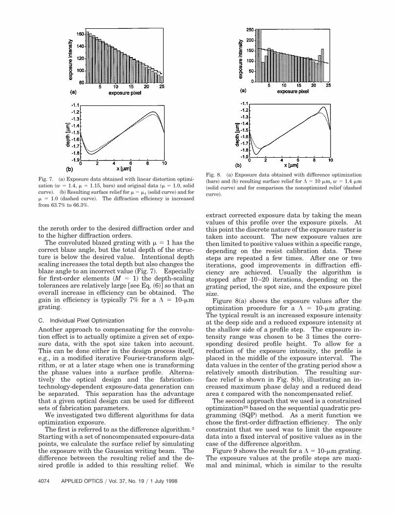
The convoluted blazed grating with m 5 1 has thecorrect blaze angle, but the total depth of the struc-ture is below the desired value. Intentional depthscaling increases the total depth but also changes theblaze angle to an incorrect value ~Fig. 7!. Especiallyfor first-order elements ~M 5 1! the depth-scalingtolerances are relatively large @see Eq. ~6!# so that anoverall increase in efficiency can be obtained. Thegain in efficiency is typically 7% for a L 5 10-mmgrating.
C. Individual Pixel Optimization
Another approach to compensating for the convolu-tion effect is to actually optimize a given set of expo-sure data, with the spot size taken into account.This can be done either in the design process itself,e.g., in a modified iterative Fourier-transform algo-rithm, or at a later stage when one is transformingthe phase values into a surface profile. Alterna-tively the optical design and the fabrication-technology-dependent exposure-data generation canbe separated. This separation has the advantagethat a given optical design can be used for differentsets of fabrication parameters.
We investigated two different algorithms for dataoptimization exposure.
The first is referred to as the difference algorithm.3Starting with a set of noncompensated exposure-datapoints, we calculate the surface relief by simulatingthe exposure with the Gaussian writing beam. Thedifference between the resulting relief and the de-sired profile is added to this resulting relief. We
Fig. 7. ~a! Exposure data obtained with linear distortion optimi-zation ~w 5 1.4, m 5 1.15, bars! and original data ~m 5 1.0, solidcurve!. ~b! Resulting surface relief for m 5 m1 ~solid curve! and form 5 1.0 ~dashed curve!. The diffraction efficiency is increasedfrom 63.7% to 66.3%.
4074 APPLIED OPTICS y Vol. 37, No. 19 y 1 July 1998
extract corrected exposure data by taking the meanvalues of this profile over the exposure pixels. Atthis point the discrete nature of the exposure raster istaken into account. The new exposure values arethen limited to positive values within a specific range,depending on the resist calibration data. Thesesteps are repeated a few times. After one or twoiterations, good improvements in diffraction effi-ciency are achieved. Usually the algorithm isstopped after 10–20 iterations, depending on thegrating period, the spot size, and the exposure pixelsize.
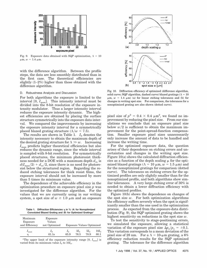
Figure 8~a! shows the exposure values after theoptimization procedure for a L 5 10-mm grating.The typical result is an increased exposure intensityat the deep side and a reduced exposure intensity atthe shallow side of a profile step. The exposure in-tensity range was chosen to be 3 times the corre-sponding desired profile height. To allow for areduction of the exposure intensity, the profile isplaced in the middle of the exposure interval. Thedata values in the center of the grating period show arelatively smooth distribution. The resulting sur-face relief is shown in Fig. 8~b!, illustrating an in-creased maximum phase delay and a reduced deadarea ε compared with the noncompensated relief.
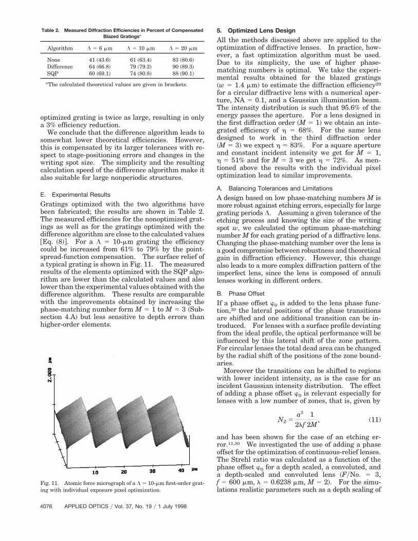
The second approach that we used is a constrainedoptimization28 based on the sequential quadratic pro-gramming ~SQP! method. As a merit function wechose the first-order diffraction efficiency. The onlyconstraint that we used was to limit the exposuredata into a fixed interval of positive values as in thecase of the difference algorithm.
Figure 9 shows the result for a L 5 10-mm grating.The exposure values at the profile steps are maxi-mal and minimal, which is similar to the results
Fig. 8. ~a! Exposure data obtained with difference optimization~bars! and ~b! resulting surface relief for L 5 10 mm, w 5 1.4 mm~solid curve! and for comparison the nonoptimized relief ~dashedcurve!.
with the difference algorithm. Between the profilesteps, the data are less smoothly distributed than inthe first case. The theoretical efficiencies areslightly ~1–2%! higher than those obtained with thedifference algorithm.
D. Robustness Analysis and Discussion
For both algorithms the exposure is limited to theinterval @0, Imax#. This intensity interval must bedivided into the 8-bit resolution of the exposure in-tensity modulator. Thus a larger intensity intervalreduces the exposure intensity dynamic. The high-est efficiencies are obtained by placing the surfacestructure symmetrically into the exposure data inter-val. We compared the improvements by increasingthe exposure intensity interval for a symmetricallyplaced blazed grating structure ~Lyw 5 7.5!.
The results are shown in Table 1. I0 denotes theintensity necessary to obtain the maximum depth ofthe desired grating structure for L .. w. IncreasingImax predicts higher theoretical efficiencies but alsoreduces the dynamic range, since the whole intervalis sampled with 8-bit resolution. For symmetricallyplaced structures, the minimum photoresist thick-ness needed for a DOE with a maximum depth dm isd~Imaxy2! 1 dmy2, since there is no need for photore-sist below the structured region. Regarding the re-duced etching tolerances for thick resist films, theexposure interval should not be increased by morethan 5 times its minimum value.
The dependence of the achievable efficiency in theoptimization procedure on exposure pixel size p wasinvestigated for the difference algorithm. For thevalues that we are currently using in our writingsystem, a spot size of w $ 1.0 mm and an exposure
Fig. 9. Exposure data obtained with SQP optimization, L 5 10mm, w 5 1.4 mm.
Table 1. Diffraction Efficiencies h in % ~A! for NonoptimizedConvoluted Blazed Grating and ~B! for Optimized Gratingsa
MaximumExposure
and Efficiency
ExposureValues
not Optimized Exposure Values Optimized
Imax I0 I0 3I0 5I0 10I0
h 61.1s 65.9 76.5 78.9 80.1
aThe upper limit of the exposure intensity range @0, Imax# isvaried from its minimum value I0 to 10I0.
pixel size of p2 5 0.4 3 0.4 mm2, we found no im-provement by reducing the pixel size. From our sim-ulations we conclude that an exposure pixel sizebelow wy2 is sufficient to obtain the maximum im-provement for the point-spread-function compensa-tion. Smaller exposure pixel sizes unnecessarilyonly increase the amount of data to be handled andincrease the writing time.
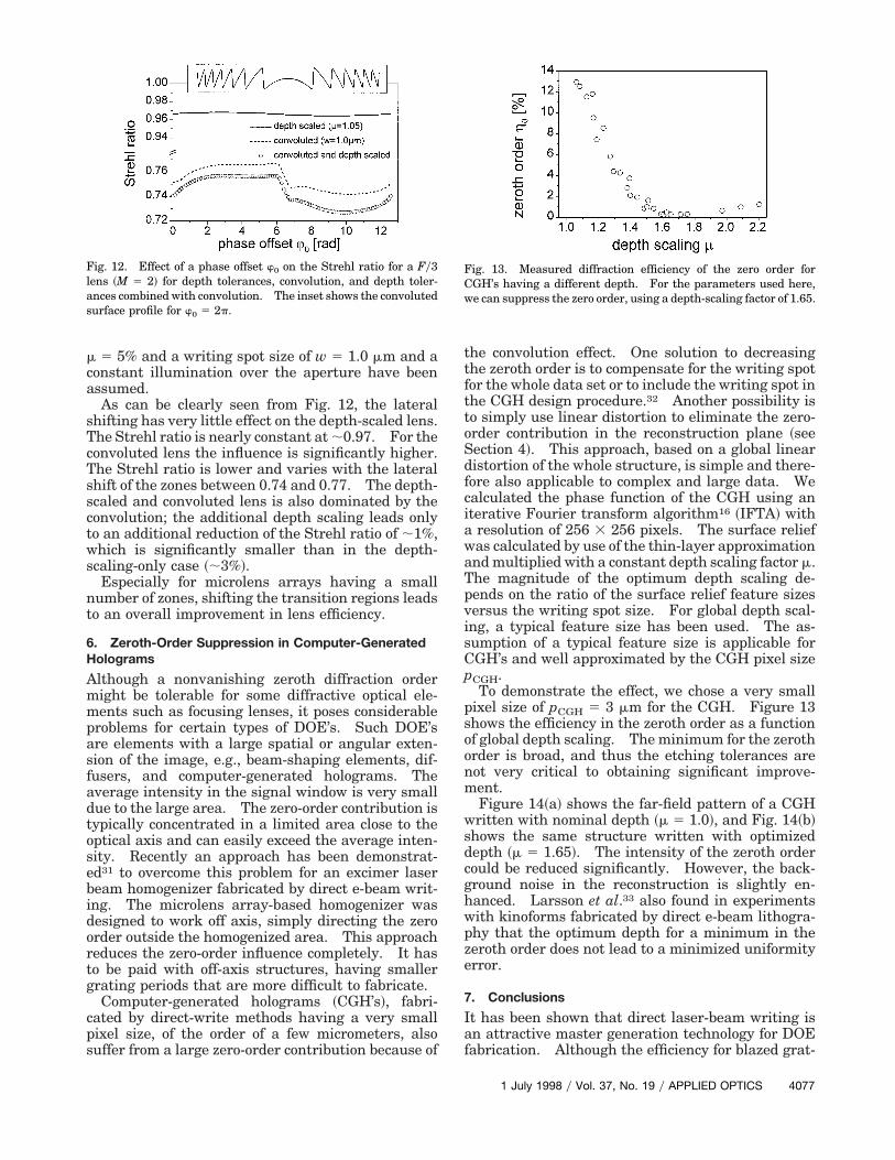
For the optimized exposure data, the questionarises of their dependence on etching errors and un-certainties and changes in the writing spot size.Figure 10~a! shows the calculated diffraction efficien-cies as a function of the depth scaling m for the opti-mized blazed gratings ~L 5 10 mm, w 5 1.5 mm! andfor the nonoptimized gratings for comparison ~dottedcurve!. The tolerances on etching errors for the op-timized profiles are only slightly smaller than for thenonoptimized profile, and both algorithms show sim-ilar tolerances. A very large etching error of 30% isneeded to obtain a lower diffraction efficiency withthe optimized profiles.
Figure 10~b! shows the dependence on changes ofthe spot size w. For both optimization algorithmsthe efficiency suffers severely when the spot is signif-icantly smaller than the one used in the optimizationprocess. As expected from the exposure-data distri-bution ~Fig. 9!, the SQP optimized grating shows thehighest sensitivity on reductions in the spot size w.
To test the sensitivity to stage-positioning errors,we simulated the exposure, allowing a statisticalvariation of the exposure pixel size Dpxypx 5 60.1.This variation corresponds to a mean deviation of thepixel size of 28 nm. For a L 5 10-mm grating, a 6%efficiency reduction results for the SQP optimizedgrating. The tolerance for the difference algorithm
Fig. 10. Diffraction efficiency of optimized ~difference algorithm,solid curve; SQP algorithm, dashed curve! blazed gratings ~L 5 10mm, w 5 1.4 mm! ~a! for linear etching tolerances and ~b! forchanges in writing spot size. For comparison, the tolerances for anonoptimized grating are also shown ~dotted curve!.
1 July 1998 y Vol. 37, No. 19 y APPLIED OPTICS 4075
optimized grating is twice as large, resulting in onlya 3% efficiency reduction.
We conclude that the difference algorithm leads tosomewhat lower theoretical efficiencies. However,this is compensated by its larger tolerances with re-spect to stage-positioning errors and changes in thewriting spot size. The simplicity and the resultingcalculation speed of the difference algorithm make italso suitable for large nonperiodic structures.
E. Experimental Results
Gratings optimized with the two algorithms havebeen fabricated; the results are shown in Table 2.The measured efficiencies for the nonoptimized grat-ings as well as for the gratings optimized with thedifference algorithm are close to the calculated values@Eq. ~8!#. For a L 5 10-mm grating the efficiencycould be increased from 61% to 79% by the point-spread-function compensation. The surface relief ofa typical grating is shown in Fig. 11. The measuredresults of the elements optimized with the SQP algo-rithm are lower than the calculated values and alsolower than the experimental values obtained with thedifference algorithm. These results are comparablewith the improvements obtained by increasing thephase-matching number form M 5 1 to M 5 3 ~Sub-section 4.A! but less sensitive to depth errors thanhigher-order elements.
Table 2. Measured Diffraction Efficiencies in Percent of CompensatedBlazed Gratingsa
Algorithm L 5 6 mm L 5 10 mm L 5 20 mm
None 41 ~43.6! 61 ~63.4! 83 ~80.6!Difference 64 ~66.8! 79 ~79.2! 90 ~89.3!SQP 60 ~69.1! 74 ~80.8! 88 ~90.1!
aThe calculated theoretical values are given in brackets.
Fig. 11. Atomic force micrograph of a L 5 10-mm first-order grat-ing with individual exposure pixel optimization.
4076 APPLIED OPTICS y Vol. 37, No. 19 y 1 July 1998
5. Optimized Lens Design
All the methods discussed above are applied to theoptimization of diffractive lenses. In practice, how-ever, a fast optimization algorithm must be used.Due to its simplicity, the use of higher phase-matching numbers is optimal. We take the experi-mental results obtained for the blazed gratings~w 5 1.4 mm! to estimate the diffraction efficiency29
for a circular diffractive lens with a numerical aper-ture, NA 5 0.1, and a Gaussian illumination beam.The intensity distribution is such that 95.6% of theenergy passes the aperture. For a lens designed inthe first diffraction order ~M 5 1! we obtain an inte-grated efficiency of h 5 68%. For the same lensdesigned to work in the third diffraction order~M 5 3! we expect h 5 83%. For a square apertureand constant incident intensity we get for M 5 1,h 5 51% and for M 5 3 we get h 5 72%. As men-tioned above the results with the individual pixeloptimization lead to similar improvements.
A. Balancing Tolerances and Limitations
A design based on low phase-matching numbers M ismore robust against etching errors, especially for largegrating periods L. Assuming a given tolerance of theetching process and knowing the size of the writingspot w, we calculated the optimum phase-matchingnumber M for each grating period of a diffractive lens.Changing the phase-matching number over the lens isa good compromise between robustness and theoreticalgain in diffraction efficiency. However, this changealso leads to a more complex diffraction pattern of theimperfect lens, since the lens is composed of annulilenses working in different orders.
B. Phase Offset
If a phase offset w0 is added to the lens phase func-tion,30 the lateral positions of the phase transitionsare shifted and one additional transition can be in-troduced. For lenses with a surface profile deviatingfrom the ideal profile, the optical performance will beinfluenced by this lateral shift of the zone pattern.For circular lenses the total dead area can be changedby the radial shift of the positions of the zone bound-aries.
Moreover the transitions can be shifted to regionswith lower incident intensity, as is the case for anincident Gaussian intensity distribution. The effectof adding a phase offset w0 is relevant especially forlenses with a low number of zones, that is, given by
NZ 5a2
2lf1
2M, (11)
and has been shown for the case of an etching er-ror.11,30 We investigated the use of adding a phaseoffset for the optimization of continuous-relief lenses.The Strehl ratio was calculated as a function of thephase offset w0 for a depth scaled, a convoluted, anda depth-scaled and convoluted lens ~FyNo. 5 3,f 5 600 mm, l 5 0.6238 mm, M 5 2!. For the simu-lations realistic parameters such as a depth scaling of
m 5 5% and a writing spot size of w 5 1.0 mm and aconstant illumination over the aperture have beenassumed.
As can be clearly seen from Fig. 12, the lateralshifting has very little effect on the depth-scaled lens.The Strehl ratio is nearly constant at ;0.97. For theconvoluted lens the influence is significantly higher.The Strehl ratio is lower and varies with the lateralshift of the zones between 0.74 and 0.77. The depth-scaled and convoluted lens is also dominated by theconvolution; the additional depth scaling leads onlyto an additional reduction of the Strehl ratio of ;1%,which is significantly smaller than in the depth-scaling-only case ~;3%!.
Especially for microlens arrays having a smallnumber of zones, shifting the transition regions leadsto an overall improvement in lens efficiency.
6. Zeroth-Order Suppression in Computer-GeneratedHolograms
Although a nonvanishing zeroth diffraction ordermight be tolerable for some diffractive optical ele-ments such as focusing lenses, it poses considerableproblems for certain types of DOE’s. Such DOE’sare elements with a large spatial or angular exten-sion of the image, e.g., beam-shaping elements, dif-fusers, and computer-generated holograms. Theaverage intensity in the signal window is very smalldue to the large area. The zero-order contribution istypically concentrated in a limited area close to theoptical axis and can easily exceed the average inten-sity. Recently an approach has been demonstrat-ed31 to overcome this problem for an excimer laserbeam homogenizer fabricated by direct e-beam writ-ing. The microlens array-based homogenizer wasdesigned to work off axis, simply directing the zeroorder outside the homogenized area. This approachreduces the zero-order influence completely. It hasto be paid with off-axis structures, having smallergrating periods that are more difficult to fabricate.
Computer-generated holograms ~CGH’s!, fabri-cated by direct-write methods having a very smallpixel size, of the order of a few micrometers, alsosuffer from a large zero-order contribution because of
Fig. 12. Effect of a phase offset w0 on the Strehl ratio for a Fy3lens ~M 5 2! for depth tolerances, convolution, and depth toler-ances combined with convolution. The inset shows the convolutedsurface profile for w0 5 2p.
the convolution effect. One solution to decreasingthe zeroth order is to compensate for the writing spotfor the whole data set or to include the writing spot inthe CGH design procedure.32 Another possibility isto simply use linear distortion to eliminate the zero-order contribution in the reconstruction plane ~seeSection 4!. This approach, based on a global lineardistortion of the whole structure, is simple and there-fore also applicable to complex and large data. Wecalculated the phase function of the CGH using aniterative Fourier transform algorithm16 ~IFTA! witha resolution of 256 3 256 pixels. The surface reliefwas calculated by use of the thin-layer approximationand multiplied with a constant depth scaling factor m.The magnitude of the optimum depth scaling de-pends on the ratio of the surface relief feature sizesversus the writing spot size. For global depth scal-ing, a typical feature size has been used. The as-sumption of a typical feature size is applicable forCGH’s and well approximated by the CGH pixel sizepCGH.
To demonstrate the effect, we chose a very smallpixel size of pCGH 5 3 mm for the CGH. Figure 13shows the efficiency in the zeroth order as a functionof global depth scaling. The minimum for the zerothorder is broad, and thus the etching tolerances arenot very critical to obtaining significant improve-ment.
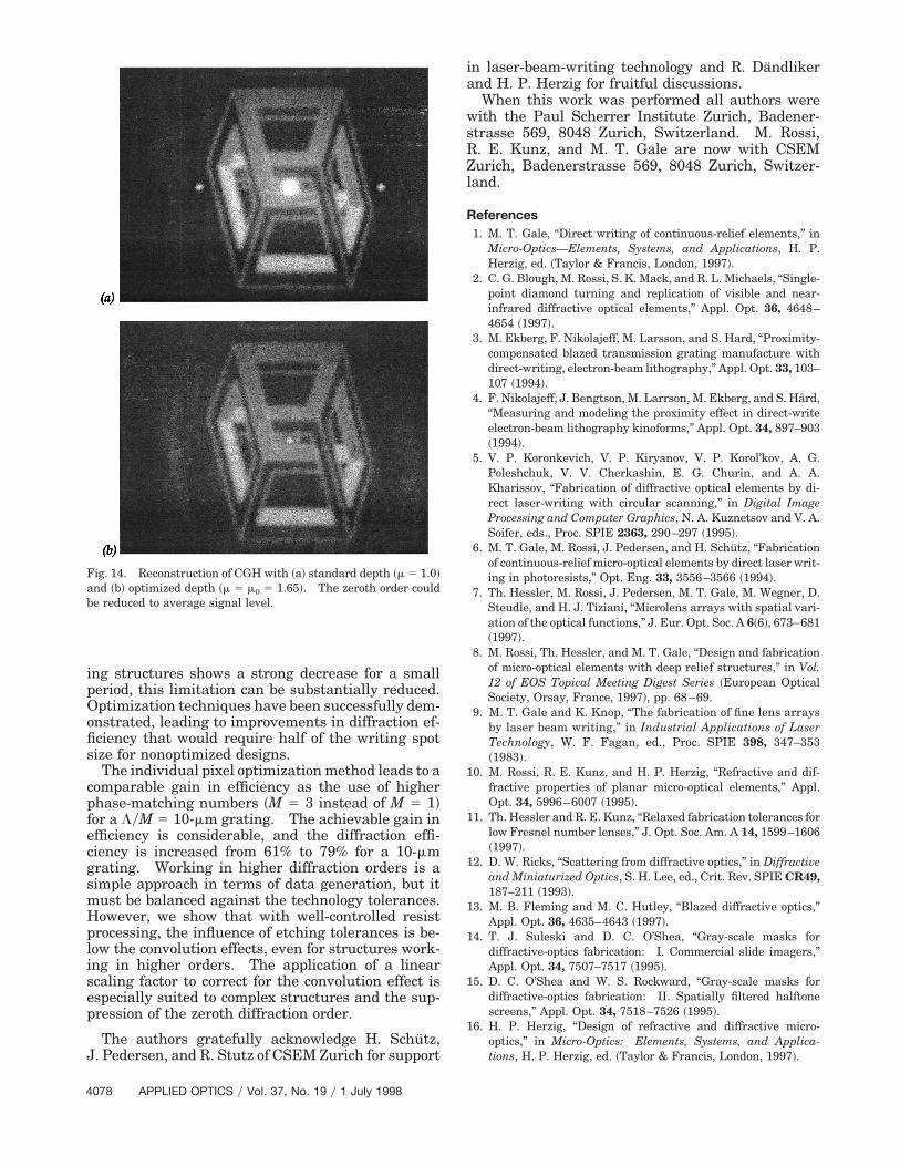
Figure 14~a! shows the far-field pattern of a CGHwritten with nominal depth ~m 5 1.0!, and Fig. 14~b!shows the same structure written with optimizeddepth ~m 5 1.65!. The intensity of the zeroth ordercould be reduced significantly. However, the back-ground noise in the reconstruction is slightly en-hanced. Larsson et al.33 also found in experimentswith kinoforms fabricated by direct e-beam lithogra-phy that the optimum depth for a minimum in thezeroth order does not lead to a minimized uniformityerror.
7. Conclusions
It has been shown that direct laser-beam writing isan attractive master generation technology for DOEfabrication. Although the efficiency for blazed grat-
Fig. 13. Measured diffraction efficiency of the zero order forCGH’s having a different depth. For the parameters used here,we can suppress the zero order, using a depth-scaling factor of 1.65.
1 July 1998 y Vol. 37, No. 19 y APPLIED OPTICS 4077
ing structures shows a strong decrease for a smallperiod, this limitation can be substantially reduced.Optimization techniques have been successfully dem-onstrated, leading to improvements in diffraction ef-ficiency that would require half of the writing spotsize for nonoptimized designs.
The individual pixel optimization method leads to acomparable gain in efficiency as the use of higherphase-matching numbers ~M 5 3 instead of M 5 1!for a LyM 5 10-mm grating. The achievable gain inefficiency is considerable, and the diffraction effi-ciency is increased from 61% to 79% for a 10-mmgrating. Working in higher diffraction orders is asimple approach in terms of data generation, but itmust be balanced against the technology tolerances.However, we show that with well-controlled resistprocessing, the influence of etching tolerances is be-low the convolution effects, even for structures work-ing in higher orders. The application of a linearscaling factor to correct for the convolution effect isespecially suited to complex structures and the sup-pression of the zeroth diffraction order.
The authors gratefully acknowledge H. Schutz,J. Pedersen, and R. Stutz of CSEM Zurich for support
Fig. 14. Reconstruction of CGH with ~a! standard depth ~m 5 1.0!and ~b! optimized depth ~m 5 m0 5 1.65!. The zeroth order couldbe reduced to average signal level.
4078 APPLIED OPTICS y Vol. 37, No. 19 y 1 July 1998
in laser-beam-writing technology and R. Dandlikerand H. P. Herzig for fruitful discussions.
When this work was performed all authors werewith the Paul Scherrer Institute Zurich, Badener-strasse 569, 8048 Zurich, Switzerland. M. Rossi,R. E. Kunz, and M. T. Gale are now with CSEMZurich, Badenerstrasse 569, 8048 Zurich, Switzer-land.
References1. M. T. Gale, “Direct writing of continuous-relief elements,” in
Micro-Optics—Elements, Systems, and Applications, H. P.Herzig, ed. ~Taylor & Francis, London, 1997!.
2. C. G. Blough, M. Rossi, S. K. Mack, and R. L. Michaels, “Single-point diamond turning and replication of visible and near-infrared diffractive optical elements,” Appl. Opt. 36, 4648–4654 ~1997!.
3. M. Ekberg, F. Nikolajeff, M. Larsson, and S. Hard, “Proximity-compensated blazed transmission grating manufacture withdirect-writing, electron-beam lithography,” Appl. Opt. 33, 103–107 ~1994!.
4. F. Nikolajeff, J. Bengtson, M. Larrson, M. Ekberg, and S. Hård,“Measuring and modeling the proximity effect in direct-writeelectron-beam lithography kinoforms,” Appl. Opt. 34, 897–903~1994!.
5. V. P. Koronkevich, V. P. Kiryanov, V. P. Korol’kov, A. G.Poleshchuk, V. V. Cherkashin, E. G. Churin, and A. A.Kharissov, “Fabrication of diffractive optical elements by di-rect laser-writing with circular scanning,” in Digital ImageProcessing and Computer Graphics, N. A. Kuznetsov and V. A.Soifer, eds., Proc. SPIE 2363, 290–297 ~1995!.
6. M. T. Gale, M. Rossi, J. Pedersen, and H. Schutz, “Fabricationof continuous-relief micro-optical elements by direct laser writ-ing in photoresists,” Opt. Eng. 33, 3556–3566 ~1994!.
7. Th. Hessler, M. Rossi, J. Pedersen, M. T. Gale, M. Wegner, D.Steudle, and H. J. Tiziani, “Microlens arrays with spatial vari-ation of the optical functions,” J. Eur. Opt. Soc. A 6~6!, 673–681~1997!.
8. M. Rossi, Th. Hessler, and M. T. Gale, “Design and fabricationof micro-optical elements with deep relief structures,” in Vol.12 of EOS Topical Meeting Digest Series ~European OpticalSociety, Orsay, France, 1997!, pp. 68–69.
9. M. T. Gale and K. Knop, “The fabrication of fine lens arraysby laser beam writing,” in Industrial Applications of LaserTechnology, W. F. Fagan, ed., Proc. SPIE 398, 347–353~1983!.
10. M. Rossi, R. E. Kunz, and H. P. Herzig, “Refractive and dif-fractive properties of planar micro-optical elements,” Appl.Opt. 34, 5996–6007 ~1995!.
11. Th. Hessler and R. E. Kunz, “Relaxed fabrication tolerances forlow Fresnel number lenses,” J. Opt. Soc. Am. A 14, 1599–1606~1997!.
12. D. W. Ricks, “Scattering from diffractive optics,” in Diffractiveand Miniaturized Optics, S. H. Lee, ed., Crit. Rev. SPIE CR49,187–211 ~1993!.
13. M. B. Fleming and M. C. Hutley, “Blazed diffractive optics,”Appl. Opt. 36, 4635–4643 ~1997!.
14. T. J. Suleski and D. C. O’Shea, “Gray-scale masks fordiffractive-optics fabrication: I. Commercial slide imagers,”Appl. Opt. 34, 7507–7517 ~1995!.
15. D. C. O’Shea and W. S. Rockward, “Gray-scale masks fordiffractive-optics fabrication: II. Spatially filtered halftonescreens,” Appl. Opt. 34, 7518–7526 ~1995!.
16. H. P. Herzig, “Design of refractive and diffractive micro-optics,” in Micro-Optics: Elements, Systems, and Applica-tions, H. P. Herzig, ed. ~Taylor & Francis, London, 1997!.
17. R. E. Kunz and M. Rossi, “Phase-matched Fresnel elements,”Opt. Commun. 97, 6–9 ~1993!.
18. Th. Hessler, “Continuous-relief diffractive optical elements:design, fabrication and applications,” Ph.D. dissertation (Uni-versity of Neuchatel, Neuchatel, Switzerland, 1998).
19. E. Noponen, J. Turunen, and A. Vasara, “Electromagnetic the-ory and design of diffractive lens arrays,” J. Opt. Soc. Am. A 10,434–443 ~1993!.
20. G. J. Swanson, “Binary optics technology: Theoretical limi-tations on the diffraction efficiency of multilevel diffractiveoptical elements,” Tech. Rep. 914 ~MIT Lincoln Laboratory,Cambridge, Mass., 1991!.
21. M. Rossi, C. G. Blough, D. H. Raguin, E. K. Popov, and D.Maystre, “Diffraction efficiency of high-NA continuous-reliefdiffractive lenses,” in Diffractive Optics and Micro-Optics, Vol.5 of 1996 OSA Technical Digest Series ~Optical Society ofAmerica, Washington, D.C., 1996!, pp. 233–236.
22. J. D. Gaskill, Linear Systems, Fourier Transforms and Optics~Wiley, New York, 1978!, Chap. 10.2.
23. The CSEM laser-beam-writing system was developed at thePaul Scherrer Institute Zurich, which was merged with CSEMin July 1997.
24. M. T. Gale, “Replication,” in Micro-Optics—Elements, Systems,and Applications, H. P. Herzig, ed. ~Taylor & Francis, London,1997!.
25. M. Kuittinen, H. P. Herzig, and P. Ehbets, “Improvements in
diffraction efficiency of gratings and microlenses with contin-uous relief structures,” Opt. Commun. 120, 230–234 ~1995!.
26. T. Fujita, H. Nishihara, and J. Koyama, “Blazed gratings andFresnel lenses fabricated by electron-beam lithography,” Opt.Lett. 7, 578–580 ~1982!.
27. E. Carcole, J. Campos, I. Juvells, and S. Bosch, “Diffractionefficiency of low-resolution Fresnel encoded lenses,” Appl. Opt.33, 6741–6746 ~1994!.
28. Matlab Optimization Toolbox 1.5, The MathWorks Inc.,Natick, Mass. ~1996!.
29. D. A. Buralli and G. M. Morris, “Effects of diffraction efficiencyon the modulation transfer function of diffractive lenses,”Appl. Opt. 31, 4389–4396 ~1992!.
30. P. Ehbets, M. Rossi, and H. P. Herzig, “Continuous-relief fanout elements with optimized fabrication tolerances,” Opt. Eng.34, 3456–3464 ~1995!.
31. F. Nikolajeff, S. Hård, and B. Curtis, “Diffractive microlensesreplicated in fused silica for excimer laser-beam homogeniz-ing,” Appl. Opt. 36, 8481–8489 ~1997!.
32. J. Bengtsson, “Direct inclusion of the proximity effect in thecalculation of kinoforms,” Appl. Opt. 33, 4993–4996 ~1994!.
33. M. Larsson, M. Ekberg, F. Nikolajeff, and S. Hård, “Successivedevelopment optimization of resist kinoforms manufacturedwith direct-writing, electron-beam lithography,” Appl. Opt. 33,1176–1179 ~1994!.
1 July 1998 y Vol. 37, No. 19 y APPLIED OPTICS 4079