Embed Size (px)
Citation preview

Analysis and Optimization of Global Interconnects
Sachin SapatnekarECE Department
University of MinnesotaMinneapolis, MN, USA

Acknowledgements
Many slides borrowed from• Chuck Alpert, IBM• Jiang Hu, Texas A&M• Prashant Saxena, Synopsys
2

Outline of the talk
• Interconnect delay metrics
• Interconnects and scaling theory
• Synthesis of signal interconnects
• Noise and congestion issues
3

Simple delay metrics
4

Interconnect modeling
• Precise model requires transmission line analysis
• Break up wire into segments
• Each segment can be modeled asL-model π-model T-model
• Other issues (crosstalk etc.) modeled using coupling caps• Interconnect extraction
– Most precise with a 3-D field solver (takes a long time!)– Other faster approximate techniques useful for design
analysis/optimization (R per square, C per unit area, 2.5-D models)
R(+sL)C C/2 C/2
R(+sL)
CR/2(+sL/2) R/2(+sL/2)
dx
5

Gate delay models
• Traditionally: assume that the gate drives a capacitor– Build macromodels for individual gates
• Delay = f(widths, transition times, loads)• Example: K-factor equations• Similar idea used in standard cell characterization:
Delay = f (transition times, load)– Table lookup models: storage/accuracy tradeoff (e.g. .lib format)– Fast circuit simulation – used in many delay calculators
• More recently: effective capacitances, current source/voltage source models
6

RC delay calculations
• Delays can be calculated easily• For example: RC driven by a step excitation
Response V(t) = ( 1 - e-t/RC )Time constant = RC
Time constants for more complicated circuits?
C
RV(t)
7

Elmore delay for an RC tree
∑ ∑∈ ∈
=)( )(
,kPathi idownstreamj
jikD CRT
Ra
Rb
Rc
Rd
Re
Ca
Cb
Cc
Cd
CeRoot
– Elmore Delay to node e = Ra.(Ca+Cb+Cc+Cd+Ce) + Rb.(Cb+Cd + Ce) + Re.Ce
8

Incrementally calculating the Elmore delay
A B CR1 R2
C1 C2
22211 )()( CRCCRCADelay ++=−
9

Model order reduction methods
• Elmore delay: RC transfer functionH(s) ≈ a0
b0 + b1 s• Can approximate RC circuit transfer function as
a0 + a1 s + ... + an-1 sn-1
b0 + b1 s + ... + bn-1 sn-1 + bn sn
– Response approximated as a sum of exponentials– Useful for interconnect simulation– Other variants: PVL, PRIMA, etc.– Handles linear systems, but drivers may be nonlinear
e(t)
e’(t) t
ttd
10

Effective capacitance model
• Includes the effects of gate nonlinearities• Gate driving RC interconnect
– Determine waveform at gate output; analyze interconnect as a linear system after that
• Possible model for waveform at x– Gate driving total capacitance of net?
• Gives erroneous results due to resistive shielding– Actual effective capacitance < total wiring capacitance– Techniques exist for determining Ceffective, or modeling the gate using
a voltage/current source
xx
C1
R
C2
11

Computing Ceff: Overall flow
Cnew=Ctot
Ceff=Cnew Ceff
Compute Thevenin model at Ceff
No
12
Cnew
Match chargeTo get Cnew
Ceff=Cnew?
Computedelay,slew
yes
[C. Kashyap]

Current source model
• Represents the transistor I-V curve as a function of input slew and output load
• Linear Thevenin driver
• CCSM (Synopsys), ECSM (Cadence)
±
delay = f(slew,Cload)
rd
Vout
Iout = f(slew,Cload)
[Amin, DAC06] 13

Wire tapering and layer assignment
• Elmore delay
Root
– Wires near the root must have low resistances– Wires near the leaves must have low capacitances– Wider wires near root, narrower near leaves
• In practice: # of wire widths limited to two or three• Same principle applies to layer assignment
∑ ∑∈ ∈
=)( )(
,kPathi idownstreamj
jikD CRT
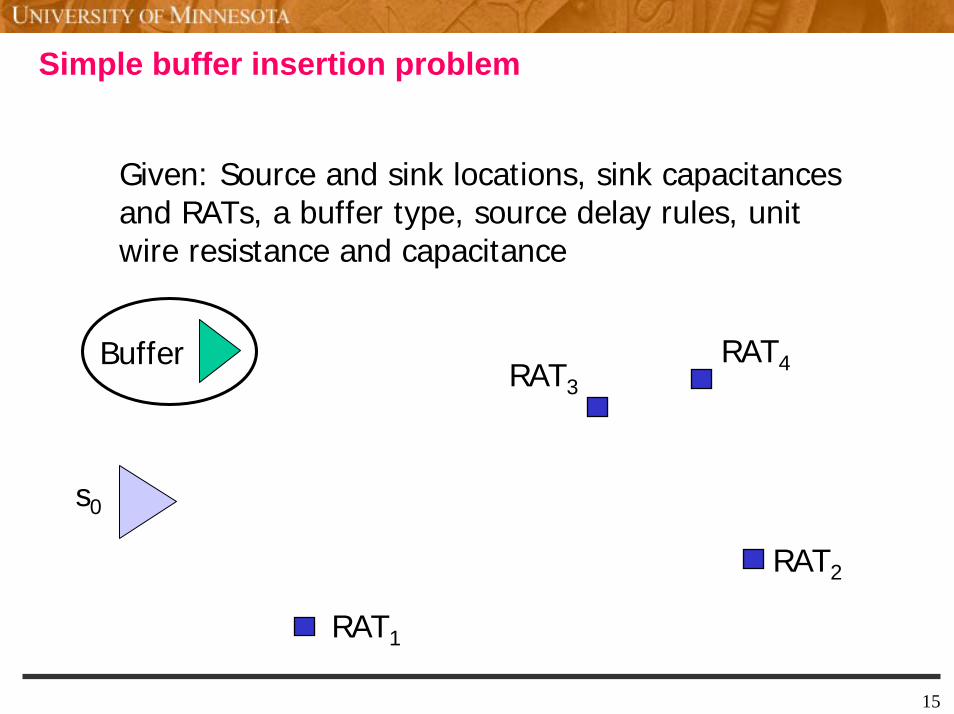
Simple buffer insertion problem
Given: Source and sink locations, sink capacitancesand RATs, a buffer type, source delay rules, unit wire resistance and capacitance
Buffer RAT4RAT3
s0
RAT2
RAT1
15

Simple buffer insertion problem
Find: Buffer locations and a routing tree such that slack at the source is minimized
)},()({min)( 0410 iii ssdelaysRATsq −= ≤≤
16
RAT2
RAT4RAT3
RAT1
s0

Slack example
RAT = 500delay = 400
slack = -200RAT = 400delay = 600
RAT = 500delay = 350
slack = +100RAT = 400delay = 300
17
Interconnects and Scaling Theory

A scaling primer
SS
GG
DD• Ideal process scaling:
– Device geometries shrink by σ (= 0.7x)• Device delay shrinks by σ
– Wire geometries shrink by σ • Resistance: ρ l/(wσ.hσ) = R/σ2
• Coupling cap: ε (hσ) l /(Sσ) = same• Capacitance to ground: similar• In each process generation
R doubles, C and Cc unchanged
• But it doesn’t quite work that way• h scales by less than σ to control R
h
w
l
S
lσ
hσ
Sσwσ

Block scaling
• Block area often stays same – # cells, # nets doubles
• Wiring histogram shape (almost) invariant – Global interconnect lengths don’t shrink– Local interconnect lengths shrink by σ

A typical chip cross-section
• Wires become “fatter” as you move to upper layers
• From one technology to the next, wire aspect ratios become more skewed
• R is controlled, at the expense of coupling capacitance
[Intel]
21

The role of interconnects
• Short interconnect– Used to connect nearby cells, Rdriver >> Rinterconnect – Minimize wire C, i.e., use short minwidth wires
• Medium to long-distance (“global”) interconnect– Rdriver ≈ Rinterconnect– Size wires to tradeoff area vs. delay– Increasing width ⇒ Capacitance increases, Resistance decreases
Need to find acceptable tradeoff - wire sizing problem• “Fat” wires
– Thicker cross-sections in higher metal layers– Useful for reducing delays for global wires– Inductance issues, sharing of limited resource

Interconnect delay scaling
• Delay of a wire of length l : τint = (rl)(cl) = rcl2 (first order)
• Local interconnects : τint : (r/σ2)(c)(lσ)2 = rcl2
– Local interconnect delay unchanged (but devices get faster)
• Global interconnects : τint : (r/σ2)(c)(l)2 = (rcl2)/σ2
– Global interconnect delay doubles – unsustainable!– Problem somewhat mitigated using buffers, using nonideal
scaling as outlined earlier
• Interconnect delay increasingly more dominant

ITRS projections
Source: ITRS, 2003Source: ITRS, 20030.1
1
10
100
250 180 130 90 65 45 32Feature size (nm)Relative
delay
Gate delay (fanout 4)Local interconnect (M1,2)Global interconnect with repeatersGlobal interconnect without repeaters
ITRS ILD Roadmap Evolution
1
2
3
4
5
0 1 2 3 4 5 6 7Technology Node (µm)
Effe
ctiv
e k
1997 ITRS1999 ITRS2003 ITRS
0.25 .045.0650.090.130.18
Industry Actual Trend
Source: Chia Hong Jan, IEDM 2003Interconnect Short Course
ITRS projections often a “best case scenario” projection

Buffer insertion
• Consider
Vs
• A buffer effectively isolates the downstream capacitance
25

Optimizing medium/long interconnects
• Delays of interconnects may become very large• Wire sizing helps to control the delay• Repeater insertion is another effective technique• Effects of a buffer
– Isolates load capacitances of different “stages”– Adds a delay
26
Cbuf
Subtree cap.CL1
Subtree cap.CL2
Cbuf
Downstream capacitance here is CL1+ Cbuf(CL2 is isolated by the buffer)
RdriverSubtree cap.
CL1
Subtree cap.CL2

Buffered global interconnects: Intuition
l
Interconnect delay = r.c.l2
Now, interconnect delay = Σ r.c.li2 < r.c.l2 (where l = Σ lj )
since Σ (lj 2) < (Σ lj )2
(Of course, account for intrinsic buffer delay also)
l1 lnl3l2

More precise analysis: Optimal inter-buffer length
• First order (lumped parasitic, Elmore delay) analysis
• Assume N identical buffers with equal inter-buffer length l (L = Nl)
• For minimum delay,
( ) ( )[ ]( ) ( )⎥⎦
⎤⎢⎣⎡ +++=
+++=
gddg
ggd
CRl
cRrCrclL
clCrlclCRNT
1
0=dldT
02 =⎥⎥⎦
⎤
⎢⎢⎣
⎡−
opt
gd
lCR
rcLrcCR
l gdopt =
L
Rd – On resistance of inverterCg – Gate input capacitancer, c – Resistance, cap. per micron
… …
lRd
Cg

Optimal interconnect delay
• Substituting lopt back into the interconnect delay expression:
( ) ( )⎥⎥⎦
⎤
⎢⎢⎣
⎡+++= gd
optdgoptopt CR
lcRrCrclLT 1
( )[ ]cRrCrcCRLT dggdopt ++= 2Delay grows linearly with L (instead of quadratically)
Buffer-to-buffer spacing reduces in successive technology nodesrcCR
l gdopt =
d
dσDumb shrink
Smart shrink

Critical inter-buffer lengths
• Study based on exhaustive SPICE simulation and projected process files (Saxena et al. TCAD’04)
• Optimally-sized uniformly for min delay – Min distance at which inserting a
buffer speeds up the line
• “Ideally shrunk” circuit requires additional buffers (0.7x vs 0.57x)
90nm 65nm 45nm 32nm
M 3M 60
0.10.20.30.40.50.60.70.80.9
1
Relative critical inter-buffer length
0.57x0.57x
586.0=σσIn line with scaling In line with scaling
theory:theory:

Buffer planning needed!
Past Present/Future31

Buffer block planning
32

Buffer block planning
33

Critical sequential lengths
• Optimized for max distance in one clock period
• Assumes:– 2x frequency scaling– Ignores setup, hold, skew
• Even with 1.4x (“Moore”) frequency scaling, critical seq. lengths shrink at ~0.62x
• “Ideally shrunk” circuit requires much new wire pipelining
(0.7x vs 0.43x / 0.62x)
90nm 65nm 45nm 32nm
M3M60
1234567
Relative critical
seq. length
0.43x0.43x

Architectural impact
• Example processor floorplan shown below
• Layout decisions affect # clock cycles required to convey a signal– Architectural decisions must be made hand-in-hand with layout
35
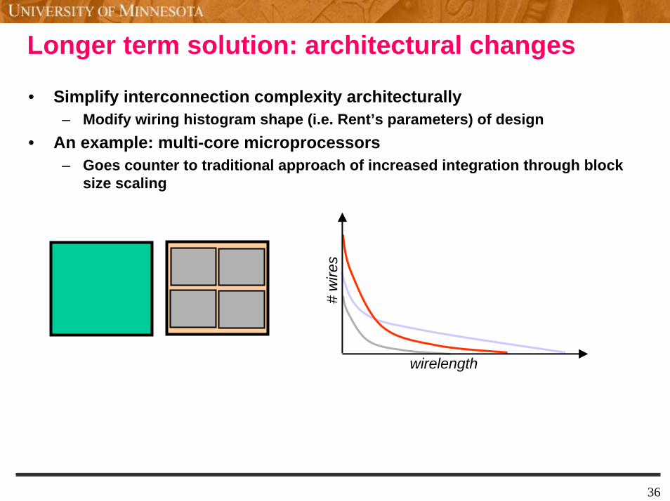
Longer term solution: architectural changes
• Simplify interconnection complexity architecturally– Modify wiring histogram shape (i.e. Rent’s parameters) of design
• An example: multi-core microprocessors– Goes counter to traditional approach of increased integration through block
size scaling
# w
ires
wirelength
36

Synthesis of Signal Interconnects

Signal interconnect synthesis
• Interconnect topology generation• Interconnect delay optimization• Noise optimization • Bus design• Congestion considerations

Van Ginneken’s classic algorithm
• Optimal for multi-sink nets• Quadratic runtime• Bottom-up from sinks to source• Generate list of candidates at each node• At source, pick the best candidate in list
39

Key assumptions
• Given routing tree• Given potential insertion points
40

Generating candidates
(1)
(2)
(3)
41

Pruning candidates
(3)
(a) (b)
Both (a) and (b) “look” the same to the source.Throw out the one with the worst slack
(4)
42

Candidate example (continued)
(4)
(5)
43
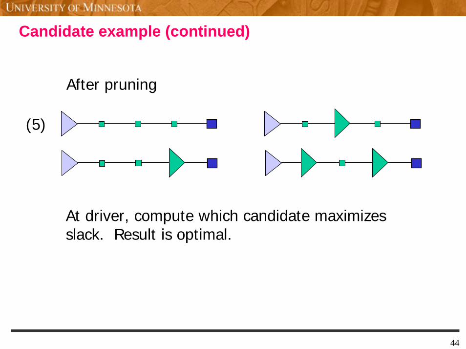
Candidate example (continued)
After pruning
(5)
At driver, compute which candidate maximizesslack. Result is optimal.
44

Merging branches
Right Candidates
Left Candidates
45
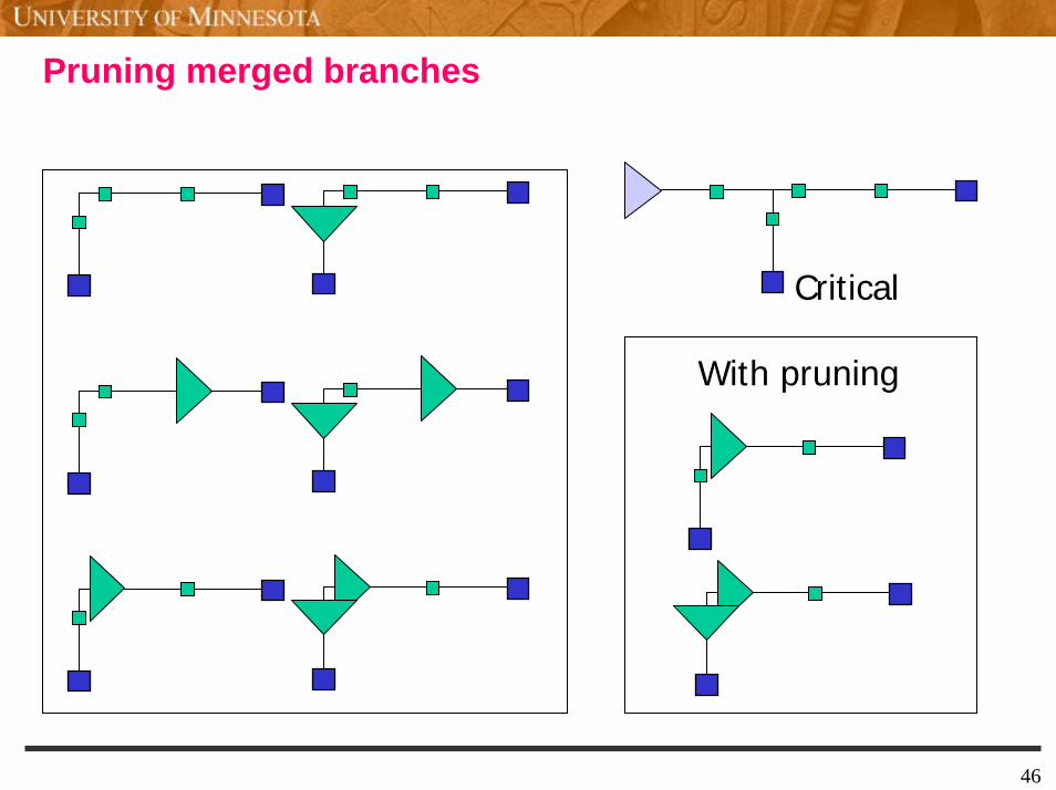
Pruning merged branches
Critical
With pruning
46

Combining the Options
• Draw a plot of all (Ck, Dk) pairs for both children m and n (assuming a binary tree)
1 3 4 5 6 72 1 3 4 5 6 72
D(m)
D(n)
C(m)
C(n)
D(combined)
C(combined)

Van Ginneken example
(20,400)WireC=10,d=150
(30,250)(5, 220)
BufferC=5, d=30
48
(20,400)
WireC=15,d=200C=15,d=120
BufferC=5, d=50C=5, d=30
(30,250)(5, 220)
(45, 50)(5, 0)(20,100)(5, 70)
(20,400)

Van Ginneken example (continued)
(30,250)(5, 220)
(45, 50)(5, 0)(20,100)(5, 70)
(20,400)
(5,0) is inferior to (5,70). (45,50) is inferior to (20,100)
(30,250)(5, 220)
(20,100)(5, 70)(30,10)
(15, -10)
Wire C=10
(20,400)
Pick solution with largest slack, follow arrows to get solution
49

Van Ginneken recap
• Generate candidates from sinks to source
• Quadratic runtime– Adding a buffer adds only one new candidate
– Merging branches additive, not multiplicative
• Optimal for Elmore delay model
50

Extensions
• Multiple buffer types• Inverters• Polarity constraints• Controlling buffer resources• Capacitance constraints• Blockage recognition• Wire sizing
51

Multiple buffer types
(1)
(2)
Time complexity increases from O(n2) to O(n2B2) where B is the number of different buffer types
52

Inverters
(1)
(2)
• Maintain a “+” and a “-” list of candidates• Only merge branches with same polarity• Throw out negative candidates at source
53

Polarity constraints
• Some sinks are positive, some negative• Put negative sinks into “-” list
“-” list
“-” list “+” list
54

Controlling buffering resources
Before, maintain list of capacitance slack pairs
(C1, q1), (C2, q2), (C3, q3) (C4, q4), (C5, q5) (C6, q6), (C7, q7), (C8, q8) (C9, q9)
Now, store an array of lists, indexed by # of buffers
3210
(C1, q1, 3), (C2, q2, 3), (C3, q3, 3)(C4, q4, 2), (C5, q5, 2)(C6, q6, 1), (C7, q7, 1), (C8, q8, 1)(C9, q9, 0)
Prune candidates with inferior cap, slack, and #buffers
55
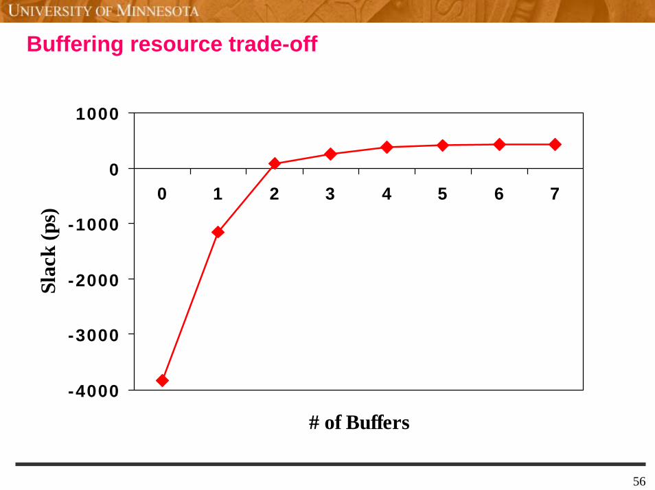
Buffering resource trade-off
-4000
-3000
-2000
-1000
0
1000
0 1 2 3 4 5 6 7
# of Buffers
Slac
k (p
s)
56
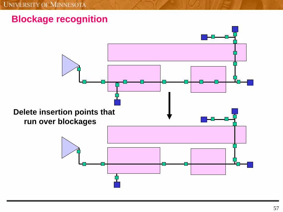
Blockage recognition
Delete insertion points that run over blockages
57

Other extensions
• Modeling effective capacitance• Higher-order interconnect delay• Slew constraints• Noise constraints
58

π-models
• Van Ginneken candidate: (Cap, slack)
Cn
R
CfC
Replace Cap with π-model (Cn, R, Cf)Total capacitance preserved: Cn + Cf = CR represents degree of resistive shielding
59

Computing gate delay
• When inserting buffer, compute effective capacitance from π-model
Ceff
Use effective instead of lumped capacitance in gate delay equationOptimality no longer guaranteed
60

Higher-order interconnect delay
• Moment matching with first 3 moments• Previously: candidate (π-model, slack)• Now: candidate (π-model, m1, m2, m3)• Given moments, compute slack on the fly• Bottom-up, efficient moment computation• Problem: guess slew rate
61

Slew constraints
• When inserting buffer, compute slews to gates driven by buffer
• If slew exceeds target, prune candidate• Difficulty: unknown gate input slew
Slew 300 ps
Slew 350 ps?
62

Timing-driven Steiner approaches
• BRBC• Prim-Dijkstra• P-Tree• A-Tree (RSA)• SERT• MVERT
63
Rectilinear Steiner arborescence
• Assume all sinks in first quadrant• Iteratively
– Find sink pair p and q maximimizing min(xp, xq) + min (yp, yq)– Remove p and q from consideration– Replace with r = min(xp, xq), min (yp, yq)– Connect p and q to r
64

RSA example
1
3
4
25
6
65

RSA diagonal line sweep
12
34
5
6
66

Prim-Dijkstra algorithm
Prim’sMST
Dijkstra’sSPT
Trade-off
67

Prim’s and Dijkstra’s algorithms
• d(i,j): length of the edge (i, j)• p(j): length of the path from source to j• Prim: d(i,j) Dijkstra: d(i,j) + p(j)
p(j)
d(i,j)
68

The Prim-Dijkstra trade-off
• Prim: add edge minimizing d(i,j)• Dijkstra: add edge minimizing p(i) + d(i,j)• Trade-off: c(p(i)) + d(i,j) for 0 <= c <= 1• When c=0, trade-off = Prim• When c=1, trade-off = Dijkstra
69

Polarity problem
_+
++
_ +
_ _
_
_
_
70

A better solution?
_+
++
_ +
_ _
_
_
_
71

Buffer aware trees
(1)
(2)
(3)
72

C-Tree algorithm
• Cluster sinks by – Polarity– Manhattan distance– Criticality
• Two-level tree– Form tree for each cluster– Form top-level tree
73

C-Tree example
74

Clustering distance metric
• pDist(i,j) = | polarity(i) – polarity(j)|• sDist(i,j) = (|xi – xj| + |yi – yj|)/diam• tDist(i,j) scaled between 0 and 1, 0 for equal criticalities, 1 for
opposite criticalities• Final distance metric d(i,j) = pDist(i,j) + βsDist(i,j) + (1-β)tDist(i,j)
75

Clustering – Finding centers
32
R
14
76

Clustering – Group to centers
3
77
R
1
2
4

Net n8702
78

Don’t avoid all blockages!
79

Buffer bays
80

Blockage avoidance example
2-path1
2-path2
2-path3
81

Blockage avoidance example
2-path1
2-path2
2-path3
82

Blockage avoidance example
2-path1
2-path2
2-path3
83
Noise and Congestion Issues
84

Crosstalk
• Crosstalk is caused due to coupling between adjacent wires in a layout– Wires have capacitors to GND and between each other– Ccoupling is of the same order of magnitude as Csubstrate
• Coupling can impact the circuit in two ways– Increased noise– Increased delays
• “Chicken-and-egg” problem: do not know coupling cap unless delays are known; do not know delays unless coupling cap is known
• Typically solved by iteration using min-max timing windows
85

Intuition
• Miller capacitance: equivalent capacitor to ground
– In reality, equivalent coupling caps of < 0 and > 2Cc may be seen; use of –C/C/3C has been proposed
Cc
0
2 Cc
Cc
Cc
Cc
aggressor
victim
aggressor
victim
aggressor
victim
[Only victim shown here]
86

Miller capacitors are an approximation!
• Real picture
Fanout gate acts as a low-pass filter! If the pulse is very sharp + occurs after the transition, it may be filtered out
Aggressor
Victim (without noise)
Victim (with noise)
Induced noise
Aggressor
Victim
87

Parameters affecting coupling noise
• “Near end” vs. “Far end”
• RC model: Vfar end > Vnear end
GND
GND
Aggressor
Victim
GND
GND
Aggressor
VictimGND
88

Noise Optimization
• Spacing• Track permutation
– Temporally non-adjacent signals made spatially adjacent
• Shielding• Downsizing aggressor driver • Upsizing victim driver• Buffering victim net• Up-layering victim net• Changing topology of victim net• Splitting fanouts of victim net
AV
Sh
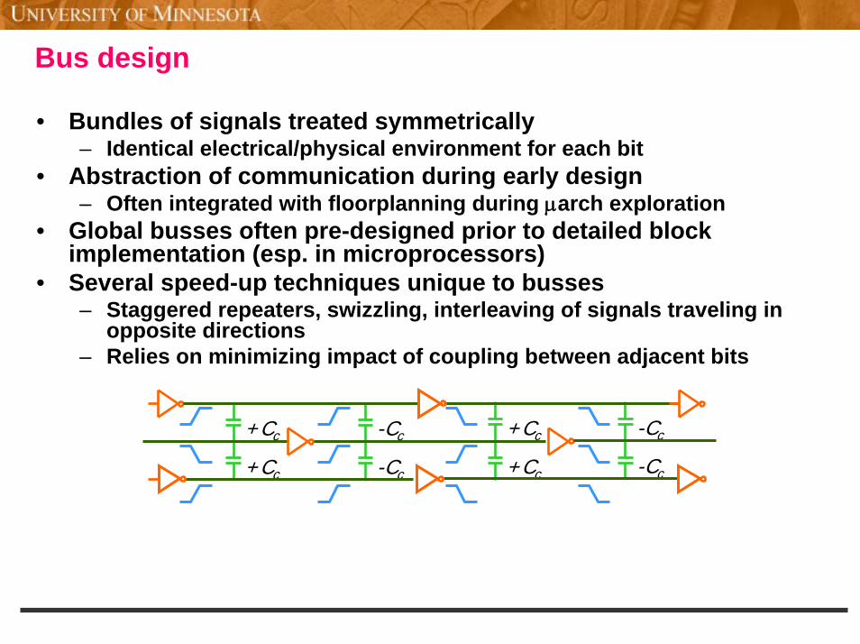
Bus design
• Bundles of signals treated symmetrically– Identical electrical/physical environment for each bit
• Abstraction of communication during early design– Often integrated with floorplanning during µarch exploration
• Global busses often pre-designed prior to detailed block implementation (esp. in microprocessors)
• Several speed-up techniques unique to busses– Staggered repeaters, swizzling, interleaving of signals traveling in
opposite directions– Relies on minimizing impact of coupling between adjacent bits
-Cc
-Cc
+Cc
+Cc
-Cc
-Cc
+Cc
+Cc

Congestion considerations
• Designs increasingly wire-limited• Interconnect optimization: routing resource intensive
– Shielding, spacing, wide-wires, up-layering• Congestion can cause detours (or even unroutable designs)• Detours increase interconnect delay as well as interconnect
delay unpredictability– Wire delay models during tech-mapping, placement are based on
shortest path routing– Detours increase convergence problems because of poor upstream
wire delay modeling
Need to model actual layers, routes for critical nets during placement

Impact on synthesis
• Wires cannot be ignored during synthesis– Fanout based load models obsolete … but wireload models still very
inaccurate– Fanouts often isolated by buffers
• Literal/gate count metrics often misleading– Area is often wire-limited– Area impact of wire-RC buffers
• Pre-layout gate sizing is wasted• Dense encodings (vs. one-hot and other sparse encodings)

Buffering and placement
• # buffers needed on a net depends on its routing
• Net routing depends on placement
• Buffer management for intra-block vs global nets– Too restrictive to treat global
routes/buffers as fixed obstructions
a b
a b
a
b

Full-chip assembly issues
What if we reduce block area to avoid wire effects?Many of the new physical synthesis problems go away
BUT# blocks increases!
(and block assembly is the hardest part of chip design!)
• Flat assembly(Fragmentation of paths across blocks)
OR• Increased hierarchy
(Lack of visibility across hierarchy levels)
0
10
20
30
40
50
60
70
80
1 0.9 0.7 0.5 0.3
Block area shrink factor
%ag
e of
repe
ater
s
45nm32nm
1 0.9 0.7 0.5 0.3
45nm
32nm05
10152025
30
35
40
Nor
mal
ized
# B
lock
s
Block area shrink factor

Integrated synthesis and placement
• Since design metrics depend heavily on layout, generate a layoutplan as early as possible
• Evolve logic and its layout in tandem (“companion placement ”)– Integrate logic synthesis / tech mapping with global placement– Embed nodes spatially through recursive logic partitioning and
placement– Long, critical wires and buffer needs identified early– Wire loads obtained using embedding of nodes– Hard to estimate area or delay of a Boolean node or FSM
• Pin positions can help– Somewhat easier at tech mapping stage…
• Most industrial physical synthesis tools involve some integration between tech mapping and placement

Congestion optimization
• Congested layouts harder to converge or unroutable– More delay from wires– Detours make upstream wire delay models more
inaccurate• Cannot model congestion by a single number
characterizing entire block– Spatial map required
• Congestion can be addressed during placement– Congestion cost in objective function– Post-placement remedies
• Recent work on congestion relief by modifying netlist structure during tech mapping– Congestion map generated bottom-up during
covering from partial maps propagated during matching
Track requirement = 12
Track requirement = 20
AOI33
(Shelar, ISPD’05)

Congestion driven supply/signal codesign
• Interconnect resources increasingly scarce– Global power and signal wires compete for routing resources
Power Wire Removal + Power Grid Sizing
Power Grid
Macros or Cells
Signal Netlists
Global Router
Congestion Map

Removal illustration
Critical wires: 1, 2, 4 and 6Non-Critical wires: 3 and 5 Removal order: first 3 then 5

Optimal power grid of “ac3”

Conclusion
• Interconnects are the primary bottleneck in design today• Many shifts in design methodology can be motivated by
interconnect-related problems (including async or NoCs)• The objective of this tutorial was to
– explain why interconnects are important– overview some fundamental algorithms in interconnect design– outline issues that a designer must worry about
100