Embed Size (px)
Citation preview
7/27/2019 Analysis of High Frequency Multi-Phase Multi-Stage Boost Converter
http://slidepdf.com/reader/full/analysis-of-high-frequency-multi-phase-multi-stage-boost-converter 1/7
ISSN (Print): 2278-8948, Volume-2, Issue-1, 2013
45
Analysis of High Frequency Multi-Phase Multi-Stage Boost Converter
Karuna Mudliyar
Manipal Institute of
Technology
Manipal, [email protected]
Suryanarayana K
Dept. of Electrical and
Electronics Engineering
NMAM Institute of Technology
Karkala, India
H.V.Gururaj Rao
Dept. of Electrical and
Electronics Engineering
Manipal Institute of Technology
Manipal, India
L.V. Prabhu, Krishnaprasad
Technical Director
HEXMOTO Controls Pvt. Ltd
Mysore, [email protected]@hexmoto.com
Abstract - A novel approach to achieve a high static gain in non-
isolated dc-dc converter is presented in this paper. The
conventional boost converter is cascaded to step-up the voltage
to higher level and the first boost stage is multi-phased to avoid
high input current stress on the switch. The multi-phase
configuration significantly reduces the current ripple and the
voltage ripple due to the operation of the parallel paths and
hence reducing the filter size. This technique allows the
operation with a high static gain and high efficiency, making
possible to design a compact circuit. The operational principle,
the design procedure and the simulation results obtained are
presented for multi-phase, multi-stage and integrated multi-
phase multi-stage boost converter.
Keywords: high step-up gain, multi-stage, multi-phase, ripple
cancellation.
I. INTRODUCTION
With the growth of battery powered application, there is a
huge demand for highly efficient, small size, low cost and
high static gain dc-dc converter. Typical applications are
hybrid vehicle, uninterrupted power supply [4] and renewableenergy system such as solar.
The step-up stage normally is the critical point for the
design of high efficiency converters due to the operation with
high input current and high output voltage, thus a detailed
study should be carried out, in order to define the topology
for a high step-up application.
Magnetic coupled classic converter such as flyback or
push-pull converter can be used to achieve high static gain
[4]. However, volume of power transformer will greatly
influence the size of converter. The leakage inductance can produce voltage stress; high switching frequency will bring
down the efficiency of the transformer itself and will cause
electromagnetic Interference (EMI), thereby reducing theconverter efficiency. Non-isolated conventional boost
converter, can provide high step-up voltage gain but with the
penalty of high voltage and current stress, high duty cycleoperation.
However, new non-isolated dc – dc converter topologies is
proposed, showing that it is possible to obtain high static gain
with low current stress and low losses, improving the
performance with respect to conventional dc-dc converter.
A new alternative for the implementation is proposed in
this paper by cascading the boost converter to get high step-up [13] and multi-phasing to avoid current stress on
semiconductor switches [9], thus designing a highly efficient
converter with simpler structure. With increase in ripple
frequency due to multi-phasing the filter size will reduce
significantly.
II.MULTIPHASE BOOST CONVERTER
The concept of interleaving is that of increasing the effective pulse frequency of any periodic power source by
synchronizing several smaller converters and operating them
with relative phase shifts [10]. In high power applications, the
voltage and current stress can easily go beyond the range that
one power device can handle. Multiple power devices
connected in parallel and/or series could be one solution.However, voltage sharing and/or current sharing are still the
concerns. Instead of paralleling power devices, paralleling
power converters is another solution which could be more
beneficial. Furthermore, with the power converter paralleling
architecture, interleaving technique comes naturally. Benefitslike harmonic cancellation, better efficiency, better thermal
performance, and high power density can be obtained [13].
With these multi-modular converters the current stress can be
divided to a level that can be handled by semiconductor
switches and reduces the ohmic component of their
conduction losses. In many applications, one major concernis the input and output filters rely almost exclusively on
tantalum capacitors due to the highest available energy-
storage-to-volume ratio [10]. However, the ESR of this filter
capacitor causes high level thermal stress from the high
switching pulsed current. The input and output filter
capacitance is usually determined by the required number of capacitors sufficient to handle the dissipation losses due to
the ripple current. Interleaving multiple converters can
significantly reduce the switching pulsed current go through
the filter capacitor. By properly choosing the channel number
and considering the duty cycle, the ripple current may be
reduced to zero. Furthermore, interleaving increases the
ripple frequency to be n (n is the total number of phase) times
the individual switching frequency.
7/27/2019 Analysis of High Frequency Multi-Phase Multi-Stage Boost Converter
http://slidepdf.com/reader/full/analysis-of-high-frequency-multi-phase-multi-stage-boost-converter 2/7
International Journal of Advanced Electrical and Electronics Engineering, (IJAEEE)
ISSN (Print): 2278-8948, Volume-2, Issue-1, 2013
46
Vin S11 S12 S13
L11
L12
L13
D11
D12
D13
C
R
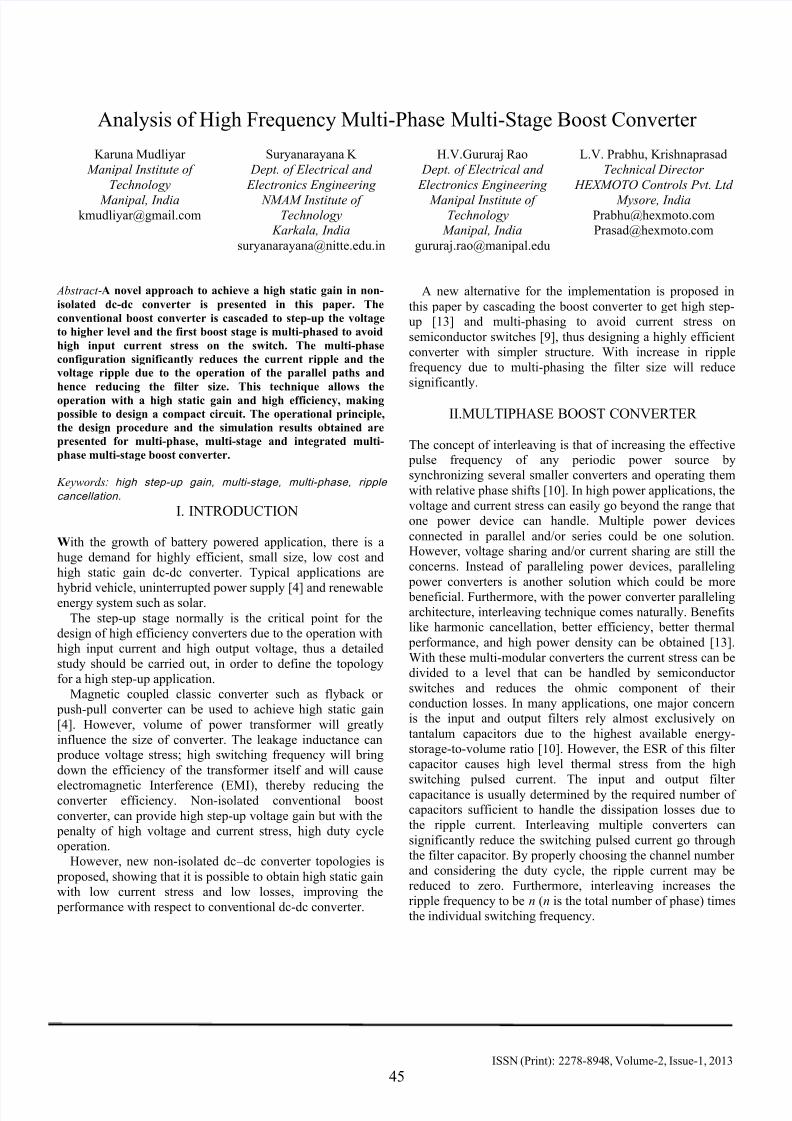
Fig.1. Three-Phase boost converter
Vin S11 S12 S13
L11
L12
L13
C R
Fig.2. Phase-1, 2, 3 closed
Vin S11 S12 S13
L11
L12
L13
C R
Fig.3. Phase-2 Open, Phase-1 and phase-3 closed.
The ESR of the tantalum capacitors is inversely proportional
to the frequency. Interleaving technique can effectively
reduce the filter capacitor size and weight. Another concern
of this application is packaging. Due to the thermal
management issues, the power loss of non-interleave
converter exceeds the typical power dissipation capability. In
addition, the substantial bulky converter usually requires a
larger heat sink module. Interleaving technique can divide the
power transfer into multiple modules, lighter and smaller.With the interleaving architecture, increased output power
may be supplied by adding additional identical modules.
Use of multi-phase boost converter is an optimal solution
for high input current dc-dc converter such as conventional
boost where the current is shared among different phases
[12]. The multi-phase booster can be achieved by addingmore parallel legs to the conventional boost converter. The
Fig.1.shows a three-phase boost converter, where two more
legs connected in parallel with the conventional one. The
multi-phase boost converter interleaves the clock signals of
the paralleled power stages, reducing input and output ripple
current without increasing the switching frequency. Because
of the phase difference in clocking between the converters,
the inductor ripple currents in the different phases tend to
cancel each other, resulting in a smaller ripple current getting
to the output capacitor. The frequency of the output ripple
current is increased by the number of the phase.
VinS11 S12 S13
L11
L12
L13
C R
Fig.4. Phase-3 Open, Phase-1 and Phase-2 closed
Vin S11 S12 S13
L11
L12
L13
C R
Fig.5. Phase-1 Open, Phase-2 and Phase-3 closed
Thus the factors, such as reduced ripple current, increased
ripple frequency contribute to a smaller output filter capacitor
for the same ripple voltage requirement, thereby reducing the
size and cost of the filter components. This results in
improved dynamic response to load transients [13].
A) Circuit description and operational analysis of Multi-
Phase Boost Converter.
The basic structure of three-phase boost converter can be
constructed by adding two parallel legs to conventional boostconverter. It is possible to add more number of parallel legs
to have more phases, where the input current is shared among
different phases. The converter is operating in continuous
conduction modes for better operational characteristics
results. Thus, the different operational stages and thetheoretical waveforms are represented for CCM and
considering three phases only. Different stage operations can
be explained with reference to the Figs.2 – 6. The three-phase
boost converter operates in six stages. The Table no.1 figures
out the status of the three-phase boost converter for different
switching conditions.In three-phase boost converter, the clock for the switches is
phase shifted by 120 degree as shown in Fig.6. The three phase ripple current waveforms are shown with solid, dashed
and dotted lines with reference to their clock signals, the
ripple cancellation among different phase’s results in reduced
magnitude and increase in frequency by three times [13].The voltage transformation of three-phase boost converter is
same as that of conventional boost converter. Due to
interleaving of the clock pulses, all the three switches are
closed for the duration − 2
3 ., three times a period with
the interval of 1 − .

7/27/2019 Analysis of High Frequency Multi-Phase Multi-Stage Boost Converter
http://slidepdf.com/reader/full/analysis-of-high-frequency-multi-phase-multi-stage-boost-converter 3/7
International Journal of Advanced Electrical and Electronics Engineering, (IJAEEE)
ISSN (Print): 2278-8948, Volume-2, Issue-1, 2013
47
Where, D and T are duty ratio and switching period of the
converter.
PHASE I
PHASE II
PHASE III
RESULTANT
RIPPLE CURRENT
INDUCTOR
CURRENTS
Fig.6. Theoretical three-phase Inductor currents
B) Design Consideration for Multi-Phase Boost Converter.
The design equations for Multi-Phase Boost converter
operating in continuous conduction mode is presented with
an example. Considering the following specifications,
Input voltage: Vin = 12 V.
Output voltage: Vout = 40 V.
Output power: P = 1KW.
Switching frequency: F = 100 kHz.
The rated load for given output power: R = 1.6 Ω
1) Static gain: The static gain of Multi-Phase booster is as
that of conventional booster.
Vout =Vin
1−D(1)
Where D is switch duty cycle ratio.
Therefore, the nominal duty cycle is 0.7
2) Inductor current : The inductor current through each phase
is given by,
IL_phase = Vout N×R.D = 27.78 A (2)
N – Number of phases.
D = 1 − D
3) Inductance: Considering 70% peak to peak ripple,
ΔIL_phase = 38.89 A
Therefore, inductance in each phase is given by
Lphase = V in .D.T
ΔIL_phase = 2.16 μH (3)
T – Switching period.
The resultant peak-to-peak ripple current through the
capacitor, is given by
Table no. 1 Switching status of Three-Phase Boost Converter
ΔIripple =V in D−2
3T
Lphase
3 = 5.56 A (4)
4) Filter capacitance: For 20% ripple voltage, the
capacitance value is given by,
C =Vout D−2
3T
ΔVout .R= 1.04 μF (5)
By considering the inductor copper loss and semiconductor
loss [7], output voltage equation for three-phase booster is
given by,
Vo
Vin= 1
D 1 − D. VD
V in 1
1+R L +D.R on +D .R D
3.R.D 2
(6)
Parasitic element values are same for all the phases, as it is
identical multi-modular structure.
VD
−diode voltage drop
RL − Inductor DC resistance RON − Switch ON resistance
Similarly, the efficiency of three-phase booster can be
computed as,
η = 1 − D .VD
V in 1
1+RL +D.R on +D .R D
3.R.D 2
(7)
Stages S11 S12 S13 Status
First
[Fig.2]
ON ON ON
All the three phase inductors
stores energy, the stored
energy in the output capacitor
is supplied to load
Second
[Fig.3] ON OFF ON
The stored energy in the
inductor L12 is transferred to
load through diode D12.
Third
[Fig.2] ON ON ON
Similar to stage 1, where all
the three phases inductors
stores energy.
Fourth
[Fig.4] ON ON OFF
The stored energy in the
inductor L13 is transferred toload through diode D13.
Fifth
[Fig.2]
ON ON ON Similar to stage 1 and 3.
Sixth[Fig.5] OFF ON ON
The stored energy in theinductor L11 is transferred to
load through diode D11.
7/27/2019 Analysis of High Frequency Multi-Phase Multi-Stage Boost Converter
http://slidepdf.com/reader/full/analysis-of-high-frequency-multi-phase-multi-stage-boost-converter 4/7
International Journal of Advanced Electrical and Electronics Engineering, (IJAEEE)
ISSN (Print): 2278-8948, Volume-2, Issue-1, 2013
48
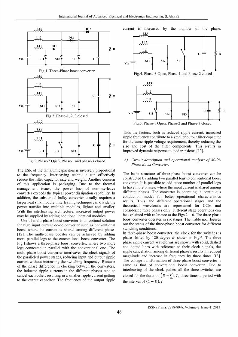
C) Simulation result of Multi-Phase Boost Converter.
The design procedure that developed was verified with
simulation results. The simulations include semiconductor
and copper loss. The Fig.7 shows the phase inductor current
and resultant ripple current waveforms. The output voltage
and current waveforms are shown in Fig.8.
514 us510 us506 us 518 us502 us
0 A
20 A
40 A
60 A
80 A
100 A
Time
IL3 IL2 IL1
Resultant ripple current
Fig.7. Three phase Inductor currents.
Time0.2 ms 0.4 ms 0.6 ms 0.8 ms 1 ms
Vout
Iout
10 V
20 V
30 V
40 V
50 V
60 V
10 A
20 A
30 A
40 A
Fig.8. Output Voltage and Current.
III.MULTISTAGE BOOST CONVERTER
In order to attain a higher boosting in conventional dc-dcconverter the required duty cycle will be very high. The
switch has to be closed for a long time so that the inductor
will store energy. But the OFF time will be in fractions,compared to ON time. The inductor has to collapse, within
the given OFF time. Very close to 100% duty cycle will
always be a threat to the system such as when the load
fluctuates or rises, the system tries to compensate the load by
increasing the duty cycle which may lead to duty ratio of 1,
means the switch has to be closed all the time, the current in
the inductor and as well in switch will continue to increase.
Thus, causing the semiconductor devices to get damaged as
the rated power dissipation exceeds [3].
Multi-Stage boost converter is a cascaded boost
converter that results in the output voltage increasing in a
geometric progression [8]. The output voltage of one stage
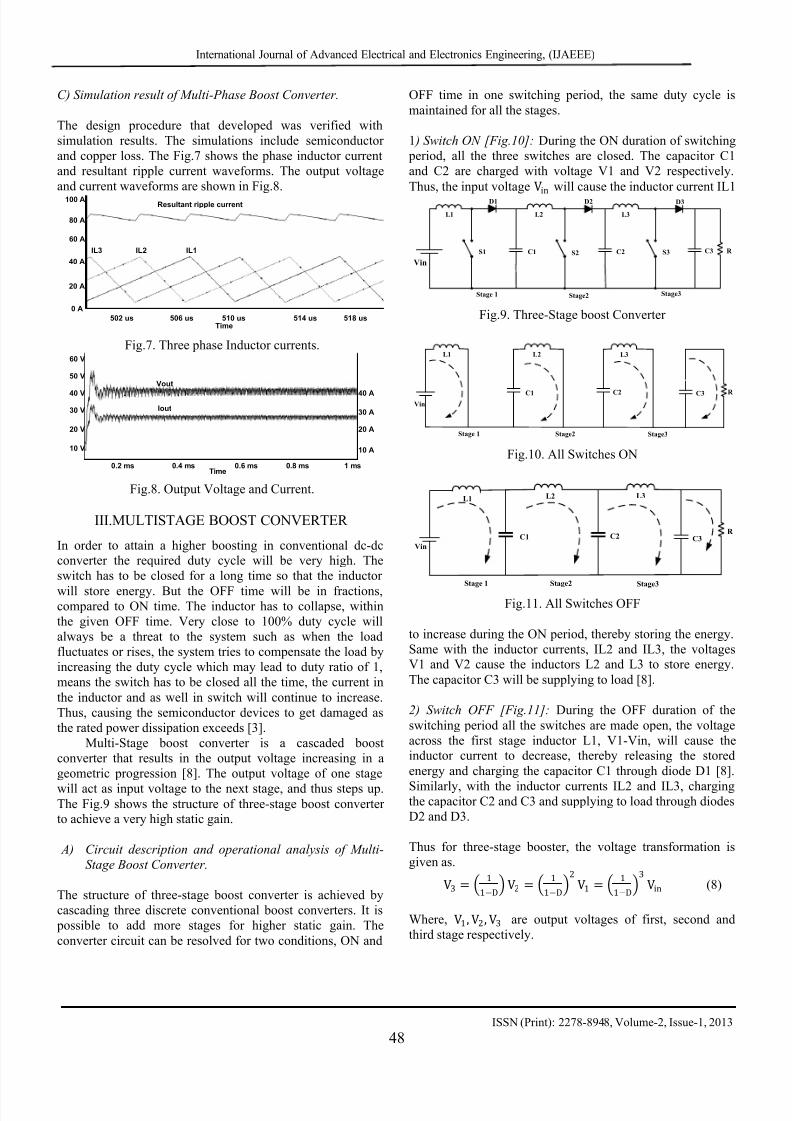
will act as input voltage to the next stage, and thus steps up.The Fig.9 shows the structure of three-stage boost converter to achieve a very high static gain.
A) Circuit description and operational analysis of Multi-
Stage Boost Converter.
The structure of three-stage boost converter is achieved by
cascading three discrete conventional boost converters. It is
possible to add more stages for higher static gain. The
converter circuit can be resolved for two conditions, ON and
OFF time in one switching period, the same duty cycle is
maintained for all the stages.
1 ) Switch ON [Fig.10]: During the ON duration of switching
period, all the three switches are closed. The capacitor C1
and C2 are charged with voltage V1 and V2 respectively.
Thus, the input voltage Vin will cause the inductor current IL1
L1 L2 L3
D1
S1 C1 C2
D2
S2
D3
C3 R S3
Stage 1 Stage2 Stage3
Vin
Fig.9. Three-Stage boost Converter
L1 L2 L3
C1 C2 C3 R
Stage 1 Stage2 Stage3
Vin
Fig.10. All Switches ON
L1 L2 L3
C1 C2 C3R
Stage 1 Stage2 Stage3
Vin
Fig.11. All Switches OFF
to increase during the ON period, thereby storing the energy.
Same with the inductor currents, IL2 and IL3, the voltagesV1 and V2 cause the inductors L2 and L3 to store energy.
The capacitor C3 will be supplying to load [8].
2) Switch OFF [Fig.11]: During the OFF duration of the
switching period all the switches are made open, the voltage
across the first stage inductor L1, V1-Vin, will cause theinductor current to decrease, thereby releasing the stored
energy and charging the capacitor C1 through diode D1 [8].
Similarly, with the inductor currents IL2 and IL3, chargingthe capacitor C2 and C3 and supplying to load through diodes
D2 and D3.
Thus for three-stage booster, the voltage transformation is
given as.
V3 = 1
1−DV2 = 1
1−D2
V1 = 1
1−D3
Vin (8)
Where, V1, V2, V3 are output voltages of first, second and
third stage respectively.

7/27/2019 Analysis of High Frequency Multi-Phase Multi-Stage Boost Converter
http://slidepdf.com/reader/full/analysis-of-high-frequency-multi-phase-multi-stage-boost-converter 5/7
International Journal of Advanced Electrical and Electronics Engineering, (IJAEEE)
ISSN (Print): 2278-8948, Volume-2, Issue-1, 2013
49
Similarly, the current relation is given by,
Io = 1 − DIL3 = 1 − D2IL2 = 1 − D3IL1 (9)
Io − output current
IL1 − first stage inductor currents.
IL2 − second stage inductor currents. IL3 − third stage inductor currents.
0.2ms
400V
200V
1ms0.8ms0.6ms0.4ms
800V
600V
Vout_1
Vout_2
Vout_3
Time
Fig.12. Output voltage of each stage
0 A
0 A50 A
100 A
150 A
0 A
15 A
30 A
Time
300 AIL1
IL2
IL3
0.2 ms 0.4 ms 0.6 ms 0.8 ms 1 ms
Fig.13. Inductor current for all stages
B) Design Consideration for Multi-Stage Boost Converter.The design equations for Multi-Stage Boost converter
operating in continuous conduction mode is presented with
an example. Considering the following specifications,
Input voltage: Vin = 12 V.
Output voltage: Vout = 444 V. Output power: P = 1KW.
Switching frequency: F = 100 kHz.The rated load for given output power: R = 197.13 Ω
1) Static gain: The static gain of Three-stage booster is given
by,
Vout = 1
1−D3
Vin (10)
Where D is switch duty cycle.
Therefore, the nominal duty cycle is 0.7
2) Intermediate Inductor currents and capacitor voltages:
First stage output capacitance voltage,
V1 = 1
1−DVin = 40 V (11)
Second stage output capacitance voltage,V2 = 1
1−D2
Vin = 133.33 V (12)
First stage inductor current,
IL1 = 1
1−D3
Io = 83.33 A (13)
Second stage inductor current,
IL2 = 1
1−D2
Io = 25 A (14)
Third stage inductor current,
IL3 = 1
1−D Io = 7.5 A (15)
3) Inductance: Considering 70% peak to peak ripple, the
inductor values are given by [7],
L1 = V in .D.T
ΔIL 1 = 0.72 μH (16)
T – Switching period.
L2 =
V1 .D.T
ΔIL2 = 8.01 μH (17)
L3 = V2 .D.T
ΔIL3 = 88.86 μH (18)
4) Capacitance: For 20% ripple voltage [7], the capacitance
value is given by,
C1 = V1 .D.T
ΔV1Req 1 = 21.06 μF (19)
C2 = V2 .D.T
ΔV2Req 2 = 1.96 μF (20)
C3 = V3 .D.T
ΔV3Req 3 = 0.17 μF (21)
C) Simulation result of Multi-stage Boost Converter.
The design procedure that developed was verified with
simulation results. The Fig.12 shows the output voltage of
every stage. The Fig.13 shows the inductor current of all the
three stages.
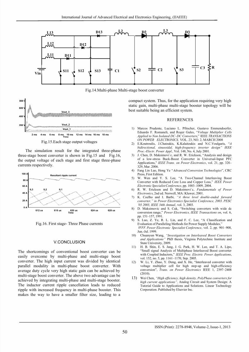
IV. MULTI-PHASE MULTI-STAGE BOOSTCONVERTER
Generally, the problem with high static gain dc-dc converter
is very high input current, power equality law [1]. The high
static gain dc-dc converter posses a high input current stress
on the switch. Thus the power semiconductor device at the
input side is always stressed by high current. In case of
Multi-stage boost converter, the first stage power
semiconductor switches are more stressed than any other. The
multi-phase booster is integrated with multi-stage booster, in
order to achieve the advantage of both modalities. Thus, the
first stage in three stage boost converter can be multi-phased,
so that the high input current can be shared among all the phases [13]. The Fig.14 shows a three-phase three-stage
boost converter, the converter provides a high static gain and
posses much less stress to the initial stage components. More
than one stage can be multi-phased if required. Thus it makes
possible to have low rated components to be used. The
increase in the number of components in multi-phase multi-stage booster is compensated by better efficiency. The heat
sink module required at high current input stage is
considerably reduced.
The design procedure is the same as discussed above
for multi-phase and multi-stage booster. The number of
stages and the number of phase in each stage will depend on
the application, the static gain and the duty cycle.
7/27/2019 Analysis of High Frequency Multi-Phase Multi-Stage Boost Converter
http://slidepdf.com/reader/full/analysis-of-high-frequency-multi-phase-multi-stage-boost-converter 6/7
International Journal of Advanced Electrical and Electronics Engineering, (IJAEEE)
ISSN (Print): 2278-8948, Volume-2, Issue-1, 2013
50
L12
L11
S11 S12 S13
D11
D12
C1
L13 D13 L2 L3
S2 S3C2C3 R
D2 D3
Vin
Fig.14.Multi-phase Multi-stage boost converter
2 ms 4 ms 6 ms 10 ms 12 ms 14 ms 16 ms 18 ms8 ms
200 V
400 V
600 V
800 V
Vout_3
Vout_2
Vout_1
Time Fig.15.Each stage output voltages
The simulation result for the integrated three-phase
three-stage boost converter is shown in Fig.15 and Fig.16,
the output voltage of each stage and first stage three-phase
currents respectively.
624 us620 us616 us 628 us612 us
0 A
20 A
40 A
60 A
80 A
100 A
Time
IL3 IL2 IL1
Resultant ripple current
Fig.16. First stage- Three Phase currents
V.CONCLUSION
The shortcomings of conventional boost converter can be
easily overcome by multi-phase and multi-stage boost
converter. The high input current was divided by identical
parallel modality in multi-phase boost converter. With
average duty cycle very high static gain can be achieved by
multi-stage boost converter. The above two advantage can beachieved by integrating multi-phase and multi-stage booster.
The inductor current ripple cancellation leads to reduced
ripple with increased frequency in multi-phase booster. This
makes the way to have a smaller filter size, leading to a
compact system. Thus, for the application requiring very high
static gain, multi-phase multi-stage booster topology will be
best suitable being an efficient system.
REFERENCES
1) Marcos Prudente, Luciano L. Pfitscher, Gustavo Emmendoerfer,
Eduardo F. Romaneli, and Roger Gules, “Voltage Multiplier Cells
Applied to Non Isolated DC – DC Converters,” IEEE TRANSACTIONS ON POWER ELECTRONICS, VOL. 23, NO. 2, MARCH 2008
2) E.Koutroulis, J.Chatzakis, K.Kalaitzakis and N.C.Voulgaris, “ A
bidirectional, sinusoidal, high- frequency inverter design” IEEE Proc.-Electr. Power Appl., Vol. 148, No. 4, July 2001.
3) J. Chen, D. Maksimovi´c, and R. W. Erickson, “Analysis and design
of a low-stress Buck-Boost Converter in Universal-Input PFC
Applications,” IEEE Trans. on Power Electronics, vol. 21, pp. 320 –
329, Mar. 2006.
4) Fang Lin Luo, Hong Ye “ Advanced Conversion Technologies”, CRCPress, First Edition.
5) W. Wen and Y. S. Lee, “A Two-Channel Interleaving Boost
Converter with Reduced Core Loss and Copper Loss,” IEEE Power
Electronic Specialist Conference, pp. 1003 – 1009, 2004.6) R. W. Erickson and D. Maksimovi´c, Fundamentals of Power
Electronics, 2nd ed. Norwell, MA: Kluwer, 2001.7) K. Coelho and I. Barbi, “A three level double-ended forward
converter,” in Power Electronics Specialist Conference, 2003. PESC
’03 2003, IEEE 34th Annual , vol. 3, 2003.8) D. Maksimovic and S. Cuk , “Switching converters with wide dc
conversion range,” Power Electronics, IEEE Transactions on, vol. 6,
pp. 151 – 157, 1991.9) S. Luo, Z. Ye, R. L. Lin, and F. C. Lee, “A Classification and
Evaluation of Paralleling Methods for Power Supply Modules,”
IEEE Power Electronic Specialist Conference, vol. 2, pp. 901 – 908,
Jun.-Jul. 1999.
10) Chuanyun Wang, “ Investigation on Interleaved Boost Convertersand Applications” PhD thesis, Virginia Polytechnic Institute and
State University, 2009.
11) H. B. Shin, E. S. Jang, J. G. Park, H. W. Lee, and T. A. Lipo,“Small signal Analysis of Multiphase Interleaved Boost converter
with Coupled Inductors,” IEEE Proc. Electric Power Applications,
vol. 152, no. 5, pp. 1161 – 1170, Sep. 2005.12) W. Li, Y. Zhao, Y. Deng, and X. He, “Interleaved converter with
voltage multiplier cell for high step-up and high-efficiency
conversion”, Trans. on Power Electronics IEEE 1, 2397 – 2408(2010).
13) Wei Chen, “High efficiency, high density, PolyPhase converters for
high current applications”, Analog Circuit and System Design: A
Tutorial Guide to Applications and Solutions. Linear Technology
Corporation. Published by Elsevier Inc.

7/27/2019 Analysis of High Frequency Multi-Phase Multi-Stage Boost Converter
http://slidepdf.com/reader/full/analysis-of-high-frequency-multi-phase-multi-stage-boost-converter 7/7
International Journal of Advanced Electrical and Electronics Engineering, (IJAEEE)
ISSN (Print): 2278-8948, Volume-2, Issue-1, 2013
51


![Bridgeless Buck-Boost PFC Converter for Multistring LED Driver€¦ · boost converter as a universal PFC converter [6]. In order to address these issues, a buck-boost converter is](https://img.pdfslide.net/doc/110x75/5eaabf2a4ab79d1e774f9005/bridgeless-buck-boost-pfc-converter-for-multistring-led-driver-boost-converter-as.jpg)