Embed Size (px)
Citation preview

Analysis of Large Pad Surface Contact Area in
Copper CMP
X. Liao 1, Y. Zhuang 1,2, L. Borucki 2, Y. Sampurno 1,2
and A. Philipossian 1,2
1 University of Arizona, Tucson AZ USA2 Araca Incorporated, Tucson AZ USA

Introduction, Previous Work and Objective
2
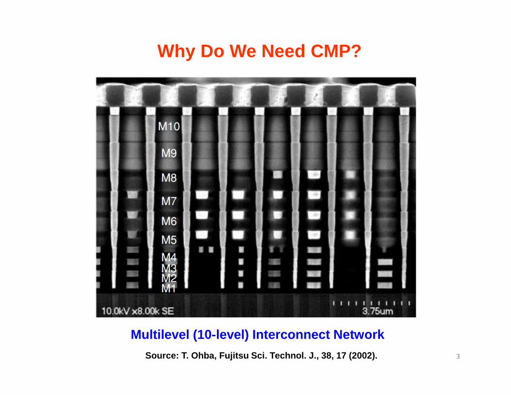
Source: T. Ohba, Fujitsu Sci. Technol. J., 38, 17 (2002).
Why Do We Need CMP?
Multilevel (10-level) Interconnect Network
3

Carrier Head Slurry Tube
Platen
Pad Conditioner
Polishing Pad
Generalized Schematic of a Rotary CMP Tool
Wafer
How Does CMP Work?
4

• There have been numerous reports that pad-wafer con tact strongly impacts material removal rate.
• Majority of previous work has shown that:
THE SMALLER THE PAD-WAFER CONTACT AREA, THE HIGHER THE MATERIAL REMOVAL RATE
• However one investigation has claimed the opposite effect to be true!
Why is Pad -Wafer Contact Area Important?
5

• Found that:
� Total pad-wafer contact area increases as a functio n of pad immersion time in pH-adjusted water.
� Local pressure on the wafer surface is reduced as immersion time and contact area increase.
� PETEOS material removal rate is consequently reduce d.
* Sematech/SRC ERC Ex-Student
Previous WorkMejia* et al.: J. Electrochem. Soc. 150 (2003) G76
6

• Found that:
� Real contact pressure in CMP is closely related wit h pad surface roughness and its composite elastic modulus .
� Real contact pressure is not related to the applied load.
• Accordingly:
� Rougher surfaces cause faster asperity wear and thu s increase the real contact area.
� Removal rate drops due to declining real contact pr essure.
Previous WorkBushan: Principles and Applications of Tribology,
John and Wiley & Sons, New York (1999)
7

• Found that:
� Pad surface wear increases the total real contact a rea.� This in turn lowers the average of the real contact pressure
at a given applied down force.� The reduction of the real contact pressure leads to a decline
in material removal rate.
Previous WorkJeong et al.: J. Adv. Mech. Dsgn. Sys. Mfg. 6 (2012) 113
8

• Found that:
� The more aggressive the conditioning process, the l ower the total pad-wafer contact area.
� Pads with lower contact areas cause PETEOS removal rate to go up during CMP.
* Sematech/SRC ERC Ex-Student
Previous WorkSun* et al.: Jpn. J. Appl. Phys. 49 (2010) 026501
9

• Found that:
� Total pad-wafer contact area decreased dramatically at higher conditioning forces.
� This led to a sharp increase in the local contact p ressure.� This consequently caused significantly higher PETEO S
removal rates during CMP.
Previous WorkLiao* et al.: Jpn. J. Appl. Phys. 52 (2013) 018001
* Sematech/SRC ERC Student
10

• Found that:*
� After a certain critical point, total pad-wafer con tact area does not contribute to TEOS material removal rate.
• Did not specify as to contact size is considered to be ‘large’ and what is considered to be ‘small’.
Previous WorkNair et al.: ICPT 2012, October 15-17, 2012, Grenoble, France
11
* Blue symbol on Slide 13

• Found totally opposite trends:*
� The lower the total pad-wafer contact area, the low er the PETEOS removal rate.
Previous WorkPark et al.: J. Electrochem. Soc. 155 (2008) H595
12
* Green symbol on Slide 13

Rem
oval
Rat
e
TOTAL Contact Area
Summary of Previous Work
Somewhat of an ‘unknown’ region!
13

• The relationship between contact area and material removal rate in CMP can be complicated.
• All previous work has focused on the TOTAL contact area, even though contact areas are very different in siz e and their characteristics. As such, each contact area s hould not be treated the same way.
• We believe that contact areas need to be studied an d classified more carefully.
• In this study we are going to classify contact area s as being ‘SMALL’ and ‘LARGE’. Sum of small and large areas is assumed to equal the total contact area.
Why Are We Focusing on ‘Large’ Contact Area?
14

Laser Confocal Microscopy
15

Zeiss LSM 510 Meta NLO
Pad surface contact area and topography analyses we re performed through
laser confocal microscopy.
Laser Confocal Microscopy
16

Laser Light
Focal PlaneReflected light near thefocal plane reaches the
Detector, but out-of-focuslight does not.
Beam splitter
Lens
Pinhole
Detector
Optical Slice
How Does a Laser Confocal Microscope Work?
17

Pad Sample
Sapphire WindowMounting Ring
Miniature Stage
Ball Bearing
Spring
Load CellThreaded Screw
Source: L. Borucki,US Patent Nos. 7,869,027 and 7,839,496
Confocal Microscope Pad Sample Holder
18

Sapphire window
Pad
Load
Contact
Contact
Near contactReflection. Notflat enough to
fringe!
Confocal Contact Area Measurements
19
Confocal optical slice
Near contact reflection or interference fringes (ze bras)
Far from contact
No reflected imageBlack area

450x450 µµµµm0.29% contact
450x450 µµµµm0.10% contact
IC 1000 Pad
Mean contact percentage is 0.076 at 1.5 PSI
Topography and Contact Area Images
20

50 µm
Example of LARGE Contact Area
21

50 µm
Topographic Analysis of LARGE Contact Area
22

SEM Analysis of a LARGE Contact Area
23

The SEM image shows that the individual large conta ct area corresponds to collapsed pore walls and loosely attached pad debri s, suggesting that the
large contact area may not be fully supported.
Detailed SEM Image of a LARGE Contact Area
24

Simulating the Young’s Modulus
25
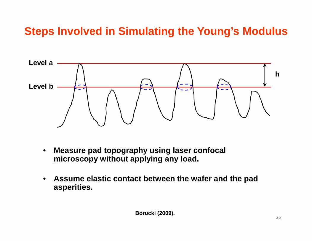
• Measure pad topography using laser confocal microscopy without applying any load.
• Assume elastic contact between the wafer and the pa d asperities.
h
Level a
Level b
Steps Involved in Simulating the Young’s Modulus
26
Borucki (2009).

• Perform a load balance based on the Greenwood and Williamson elastic model.
� Assume a certain value for the Young’s modulus.� Calculate the pressed displacement ‘h’ of the summi ts from
height level ‘a’ to some height level ‘b’ at a cert ain load.
• Contour the contact at height level ‘b’. Obtain the simulated contact area for each asperity at level ‘ b’.
• Sum up the areas of all contact contours to obtain the simulated total contact area.
• Compare simulated vs. measured contact areas. Incre ase or decrease the Young’s modulus and simulate again until the two contact areas are close enough.
Steps Involved in Simulating the Young’s Modulus
Borucki (2009).27

793 µm2
540 MPa surface
101 µm2
50 µm
300 MPa surface
50 µm
193 µm2
150 MPa surface
396 µm2
50 µm
100 MPa surface
594 µm2
50 µm
50 MPa surface
843 µm2
50 µm
Simulation Results
Borucki (2009).28

0
150
300
450
600
0 200 400 600 800 1000
Ass
ume
d Y
oung
's M
odul
us (
MP
a)
Simulated Pad Surface Contact Area ( µm 2)
Young’s Modulus vs. Surface Contact Area
Borucki (2009).29

• Individual large contact area corresponds to very l ow values of Young’s modulus (i.e. about 50 MPa).
• Such low values indicate that the pad material is s oft and the summit underlying the individual large contact area is not fully supported (as seen in the SEM image) and likely consists of fractured pore walls and loosely attach ed pad debris.
• As the soft material is very compliant, the large c ontact area implies much lower contact pressures compared to small contact area induced by fully supported pad asperities.
• As a result, large ,and low-pressure, individual co ntacts become easily lubricated and contribute less to rem oval rate than small, high-pressure contacts.
Implications of Individual ‘LARGE’ Contacts
30

An Experimental Case Study
31
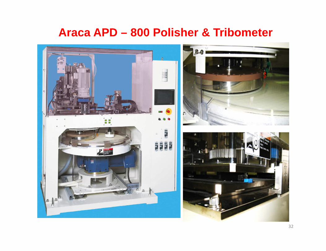
Araca APD – 800 Polisher & Tribometer
32

• Pad Conditioning
� 3M A2810 disc rotating at 95 RPM and sweeping at 10 times/min
� In-situ pad conditioning at 25.8 and 44.5 N
• Wafer Polishing
� Polishing pressure: 1.5 PSI
� Sliding velocity: 1.0 m/s
� wafer polishing time: 1.5 minute
• Pad
� IC1000 K-groove pad with Suba IV sub-pad
• Slurry
� 7 volume parts of Hitachi Chemical HS 2H635-12 slurry + 7 volume parts of DI water + 6 volume parts of ultra pure 30% hydrogen peroxide
� Flow rate: 300 ml/min
• Wafer
� 200-mm blanket copper wafers
Experimental Conditions
33

34
Removal Rate, Total Contact Area and Pad Surface Abruptness
CA 25.8 N > CA 44.5 NRR 25.8 N ~ RR 44.5 N λ 25.8 N ~ λ 44.5 N

• When asperity summits have exponentially distributed heights, then the right hand tail of the PDF will be linear on a log scale.
• The pad abruptness factor (λ) is the distance over which the tail drops by a factor of e.
• A pad with larger λ means a rougher pad contacting surface. This should result in higher removal rates.
• In our case (previous slide), RR trends are consistent with Lambda trends.
1/e
λ
35
Pad Surface Abruptness (Lambda)

Measured Total Large Contact Area Based on Contacting Asperity Threshold Size
10
100
1000
≥3 ≥4 ≥5 ≥6 ≥7 ≥8 ≥9 ≥10 ≥11 ≥12 ≥13
Mea
sure
d To
tal L
arge
Con
tact
Are
a
(µm
2 )
Threshold Size of Large Individual Contacting Asper ity (µm2)
25.8 N
44.5 N
36
Mostly due to collapsed walls and loosely attached pad debris
Collapsed walls and loosely attached pad debris see m to be removed by the high conditioning force!
Regardless of threshold size selected to define ‘LAR GE’ individual contactingasperities, there is a significant difference in th e large contact area measured
between 25.8 and 44.5 N conditioning forces, but no change in RR.

Measured Total Small Contact Area Based on Contacting Asperity Threshold Size
40
50
60
70
80
0-3 0-4 0-5 0-6 0-7 0-8 0-9 0-10 0-11 0-12 0-13
Mea
sure
d To
tal S
mal
l Con
tact
Are
a
(µm
2 )
Threshold Size of Small Individual Contacting Asper ity (µm2)
25.8 N
44.5 N
37
Pads conditioned at 25.8 and 44.5 N, share similar small contact area valueswhen 0 – 8 or 0 – 9 square micron ranges are selected to define the size of
‘SMALL’ contacting asperities.

Summary
• Individual large contact area seems to be induced b y collapsed pore walls and loosely attached pad debris.
• Simulations indicate that individual large contact areas correspond to very low values of Young’s modulus.
• A case study was presented to illustrate the role o f the individual large contact area in copper CMP.
• Results confirmed that individual large contact are a had minimal contribution to removal rate and indicated that the removal rate was mainly caused by small contact area for copper CMP.
• The case study showed that (on an IC-1000 pad) indi vidual contact areas smaller than 9 square micron contributed to r emoval rate.
• Threshold values that may define ‘SMALL’ and ‘LARGE ’ individual contact areas for different pads and processes need to be further investigated.
38

Acknowledgement
• SRC Engineering Research Center for Environmentally Benign Semiconductor Manufacturing
39