Embed Size (px)
Citation preview

Analysis of the self-imaging effect in plasmonicmultimode waveguides
André G. Edelmann, Stefan F. Helfert,* and Jürgen JahnsOptical Information Technology, FernUniversität in Hagen, Universitätsstrasse 27/PRG, 58084 Hagen, Germany
*Corresponding author: stefan.helfert@fernuni‑hagen.de
Received 16 July 2009; revised 28 September 2009; accepted 2 October 2009;posted 2 October 2009 (Doc. ID 114364); published 29 October 2009
We present studies on the propagation of plasmon waves in metallic multimode waveguides surroundedby a dielectric medium. The permittivity of themetal was determined by a Drudemodel. The propagationwas simulated by the method of lines. The propagating field exhibited the well-known self-imagingphenomenon known as the Talbot effect. The metallic waveguides are lossy. The influence of variousparameters on the losses was examined. By a suitable choice of parameters, propagation distances ofseveral Talbot periods are possible. Our investigation also includes simulations for the propagationof eigenmodes of the waveguides and results for the calculation of the effective index. © 2010 OpticalSociety of America
OCIS codes: 050.1960, 070.6760, 130.2790, 130.3120, 230.7370, 240.6680.
1. Introduction
The field of plasmonics has emerged as a new area inwhich electronics and optics merge. A plasmon is anelectromagnetic wave that propagates at optical fre-quencies along the surface of a nanoscale metallicwire [1]. Plasmonic waveguides offer the potential forminiaturization of all-optical circuits; probably bet-ter than optical high-index dielectric waveguides andsimilar to photonic crystal waveguides. As the mainlimitation of plasmonics one must consider the factthat, as a result of dissipation, only short transmis-sion distances are possible, at least with currentapproaches. The hope is to use negative-index mate-rials in the future so that long transmission dis-tances become feasible. This would open the doorto an integrated photonic–electronic circuitry. Atthe moment, a strong interest exists in modeling andsimulation of plasmonic devices. The specific chal-lenge in dealing with plasmonic propagation in com-parison with more conventional optical waveguideslies in the fact that one has to deal with large indexcontrasts and that the material parameters (here the
permittivity) can be complex with a large negativereal part.
In the past, several plasmonic devices have beenstudied. In particular we would like to mention plas-monic sensors (see, e.g., [2,3]) and plasmonic lenses(see, e.g., [4,5]). Here we consider another phenomen-on that is well known from diffraction optics, namely,the self-imaging effect. For plasmonic wave fields,self-imaging was the topic of an earlier investigation[6]. However, in that case, the considered structurewas unbounded in the lateral direction. Here, we gobeyond that case by analyzing wave propagation in aplasmonic multimode waveguide in which lateralbounding is essential. The fact that self-imaging canoccur in multimode waveguide structures is knownfrom conventional dielectric waveguides as we willexplain later.
Here, our goal is threefold: first, we analyze thepropagation of plasmonic multimode fields and studyplasmonic self-imaging to understand the physicalsituation by comparing the results with the well-known phenomenon from optics. Second, we adaptour simulation tools to this interesting situation. Thechallenge consists in the fact that here we must dealwith large dielectric index contrasts and complexmaterial parameters. As a tool for the simulation,
0003-6935/10/0700A1-10$15.00/0© 2010 Optical Society of America
1 March 2010 / Vol. 49, No. 7 / APPLIED OPTICS A1

we use the method of lines (MoL) [7,8], which is asemianalytical simulation procedure that is suitableto solve partial differential equations. In particular,the MoL has been applied to analyze waveguidestructures at microwave and optical frequencies. Inaddition, we would like to mention that the MoL hasalso been used to solve the heat equation in laserstructures [9]. Here we wish to see how well oursimulation tool is suited to simulate such lossy struc-tures or if improvements are required. Finally, theself-imaging effect in metallic multimode wave-guides might have interesting applications in laterintegrated plasmonic devices. As a specific applica-tion of self-imaging in dielectric structures, so-calledmultimode interference devices [10] have been de-monstrated as integrated beam splitters. Such beamsplitters would be required to implement signal fan-out in integrated plasmonic circuits.In Section 2 we give a brief review of self-imaging
in multimode waveguides and explain the principlesof the MoL. Section 3 shows our examined structure.Section 4 contains the focus of our study, which is thesimulation results. In particular, we examine the in-fluence of various parameters on the losses and studythe wave propagation in plasmonic waveguides. Weconclude with a summary in Section 5.
2. Theory
A. Self-Imaging in Multimode Waveguides
Self-imaging means that a wave field repeats itselfafter a certain propagation distance. A special caseof self-imaging is the Talbot effect [11], which is wellknown from optical near-field diffraction. The Talboteffect occurs for paraxial, monochromatic wave fieldswith a lateral period px. By suitable superposition ofthe modes the field repeats itself after a distance ofzT ¼ 2p2
x=λ, with λ being the wavelength, i.e.,
uðx; zÞ ¼ uðx; zþ zTÞejϕ; ð1Þwhere ϕ is a suitable phase factor that is identical forall modes. In free space, for example, it can be deter-mined as k0zT. Here, and in what follows, we use x asa transverse coordinate and z as a longitudinal coor-dinate. For the principal explanations in this sectionwe restrict ourselves to two-dimensional (2-D) struc-tures. However, in later sections we will look at thethree-dimensional (3-D) case.The Talbot effect can be observed in free space and
in multimode waveguides. In the free-space opticalcase, the lateral periodicity is imposed on the wavefield by a grating of period px. The free-space opticalTalbot effect has been widely analyzed and suggestedfor applications in interferometry [12] and for tem-poral filtering [13]. As mentioned before, the plas-monic analog was described in [6].Self-imaging in multimode waveguides was de-
scribed as early as the 1970s [14,15] and suggestedfor beam-splitting applications in the 1990s [10]. Ina waveguide, a virtual lateral periodicity exists that
is due to reflecting sidewalls. This virtual periodicityaccounts for the discrete modal spectrum of the wavefield. The periodicity is not exact since, for differentmodes, the lateral period is slightly different. This iscaused by a different extension of the modal field intothe area of the cladding for different modes (seeFig. 1). However, as shown in [16], one can describethe virtual periodicity approximately by px ≈ 2w.
The theory of self-imaging in multimode wave-guides was described in detail in [10]. Therefore, herewe restrict ourselves to a few remarks. The propaga-tion constants of the guided modes in multimodewaveguides have a (nearly) quadratic behavior withrespect to the mode number. This can be seen inFig. 1(b) where we show the normalized propagationconstant (or effective index neff ¼ kz=k0) of the modesfor the waveguide on the top. The self-imaging lengthfor an arbitrary input field can be determined fromthe difference in propagation constants of the lowest-order modes [10]. Depending on the shape of the in-put field, one can also obtain images at fractions ofthe self-imaging distance.
B. Method of Lines
For numerical analysis of the metallic structures, weuse the MoL [7,8]. The MoL has been successfully ap-plied to simulate waveguide devices in the opticaland microwave domains. The interested reader is re-ferred to two overview articles [17,18]. The analysisof plasmonic devices by different numerical methodsincluding the MoL was presented in [19–21]. Sincewe perform full 3-D calculations here, we also
Fig. 1. (Color online) (a) Dielectric multimode waveguide struc-ture and (b) normalized propagation constants of the eigenmodesfor w ¼ 20 μm, wavelength λ ¼ 1:5 μm, nco ¼ 1:52, and ncl ¼ 1:45.This waveguide was studied in [16]; the Talbot distance was deter-mined as zT ¼ 3600 μm.
A2 APPLIED OPTICS / Vol. 49, No. 7 / 1 March 2010

mention [22,23], because these papers showed howthe numerical effort can be kept moderate when ana-lyzing such 3-D structures. Here, we present just abrief summary of the MoL, which is a semianalytictechnique that operates in the frequency domain.In our computations, we assume a time dependencyaccording to expfjwtg.
To apply the MoL we start by dividing the circuitinto sections in which thematerial parameters do notdepend on the direction of the wave propagation (inour case the z direction). From Maxwell’s equationwe can then derive coupled partial differential equa-tions for the transverse components of the electric ormagnetic field (here we proceed with the magneticfield) in the following form [24]:
∂2
∂�z2~Ht −QH
~Ht ¼~0 with ~Ht ¼�
~Hy
− ~Hx
�: ð2Þ
Operator QH contains derivatives with respect to thetransverse coordinates (i.e., x; y) and the materialparameters ϵrðx; yÞ and μrðx; yÞ; see, e.g., [18]). Fur-ther, the overlined coordinates are normalized withthe free-space wavenumber k0 (e.g., �z ¼ k0z). Equa-tion (2) is a coupled partial differential equation sys-tem. To solve it, we discretize the fields in the crosssection and approximate the derivatives with respectto these coordinates with finite differences. After put-ting all the discretized fields into a supervector andcombining the finite differences into a matrix, we ob-tain a system of ordinary differential equations(ODEs):
∂2
∂�z2H−QHH ¼ 0: ð3Þ
As known from mathematics, such ODEs can besolved with a transformation to the principal axes,i.e., determining the eigenvalues and eigenvectorsof QH :
QH ¼ T−1H Γ2TH : ð4Þ
Now, by transforming the field according to
�H ¼ THH ð5Þ
and replacing QH with the expression given inEq. (4), we obtain a system of decoupled differentialequations whose solution can be easily given as
�HðzÞ ¼ e−Γ�z �Hf ð0Þ þ eΓ�z �Hbð0Þ: ð6Þ
The subscripts f and b mean forward and backward,respectively. Now, computing the eigenvalues and ei-genvectors in Eq. (3) corresponds to a determinationof the eigenmodes in the examined section. Each col-umn of the eigenvector matrix TH represents thefield distribution of these modes; the square roots ofthe eigenvalues represent the propagation constant.
For the propagation constant of the kth mode we canwrite
Γk ¼ �αk þ j�βk: ð7Þ
As previously (with the coordinates), the overbar in-dicates a normalization with k0. The denormalizedvalues are obtained by multiplication with k0ðα ¼k0�α; β ¼ k0�βÞ. Instead of Γ we often use the effectiveindex to describe the propagation of the eigenmodes.Their relation is simply given by
neff ¼ �β − j�α ¼ −jΓ: ð8Þ
As is known, the imaginary part of the effective index(�α) describes the losses. For guided modes in dielec-tric waveguides it is zero. Then �β is just the effectiveindex of the structure.
The values �Hf ;b in Eq. (6) are the complex ampli-tudes of the forward and backward propagatingmodes. Equation (5) shows how a particular field dis-tribution of these eigenmodes is put together. Equa-tion (6) is the general solution for the fields in ahomogeneous section (homogeneous section withrespect to the z coordinate). Often we have more com-plex devices that consist of more than one homoge-neous section. In this case we must apply Eqs. (2)–(6) in each of them. Next we must assure the conti-nuity of the transverse electric and magnetic fieldcomponents. Therefore, besides the magnetic fields,we must also determine the transverse electric fields�E. From Maxwell’s equations the following relationcan be derived [24]:
dd�z
E ¼ −jRHHðzÞ: ð9Þ
Similar to QH the matrix RH contains finite differ-ence approximations of derivatives with respect tox and y and the material parameters (for detailssee, e.g., [8]). Since the solution in the z directionis given in an analytic form, we can easily determinethe electric field from this equation as
EðzÞ ¼ TEð �Hf ðzÞ − �HbðzÞÞ ð10Þ
with TE ¼ jRHTHΓ−1: As said before, the overlinedmagnetic fields represent the amplitudes of the ei-genmodes. From Eq. (10) we see that the electricfields are obtained by multiplying these amplitudeswith the corresponding electric field distribution (gi-ven by TE). By enforcing the continuity of the trans-verse fields at the interfaces and assuming suitableboundary conditions, we are able to analyze completecomplicated circuits. All relevant physical phenom-ena can be included in the algorithm. Obviously, re-flections at interfaces are included, since we considerforward and backward propagating modes. To modelradiation of the fields we introduce absorbing bound-ary conditions into the finite difference expressions
1 March 2010 / Vol. 49, No. 7 / APPLIED OPTICS A3

[25]. Loss and gain of the materials are considered bycomplex numbers for the material parameters.After these introductory remarks with regard to
the MoL, we wish to emphasize one of the relevantaspects of this work. For the plasmonic devices con-sidered here, the important question is whether oursimulation method had to be further extended tohandle the large contrast differences in materialparameters and negative real values of the permit-tivity. As we show in the following, at least for thedevices examined here, the MoL proved to be a com-pletely adequate tool.
3. Model of the Examined Structure
To study the properties of the plasmon wave propa-gation we use the structure shown in Fig. 2(a) as thebasis. It consists of a metal core and a surroundingdielectric material. In general, this material could,for example, differ above and below the metal. Here,we just examined the symmetric case. The permittiv-ity of the metal was determined from a Drude model:
ϵm ¼ ϵ∞ −ω2p
ω2 − jγω : ð11Þ
Note that, because of the time dependency accordingto expfjωtg, the imaginary part of ϵm is less than zeroin the case of lossy material, which is why there is anegative sign in front of γ in Eq. (11). We would like to
point out that slightly different values for the para-meters can be found in the literature. Here we usethe following parameters taken from [20]: ϵ∞ ¼3:36174, ωp ¼ 1:3388 × 1016 s−1, and γ ¼ 7:07592×1013 s−1. ϵr as a function of the wavelength in the op-tical regime is presented in Fig. 2(b). We see that thereal part as well as the imaginary part is negativeand that their absolute value increases with increas-ing wavelength. In the following simulations, severalof the parameters in Fig. 2(a) will be varied to eval-uate their influence on the waveguide losses.
A. Eigenmodes of Multimode Waveguides
As described in Subsection 2.A, more than twoguided modes with different k vectors are requiredto obtain the self-imaging effect. Therefore, we startwith a comparison of the eigenmodes in dielectricand metallic waveguides. The dielectric structure weuse for comparison is similar to the metallic oneshown in Fig. 2. Instead of a metallic core with thepermittivity ϵm however, the core consists of a dielec-tric. Furthermore, height t is different.
As is usual in optics, we consider materials withμr ¼ 1. The wavelength was chosen to be λ ¼600nm. The other parameters are: waveguide widthw ¼ 2 μm and permittivity of the surrounding mate-rial ϵd ¼ 4. For the dielectric waveguide we chose thevalue of 2:22 ¼ 4:84 for the relative permittivity inthe core and the height t ¼ 0:5 μm. For comparison,for the metallic waveguide we use ϵm ¼ −14:7897 −
j0:4088 and t ¼ 0:1 μm.The magnetic field distributions of the significant
eigenmodes are shown in Fig. 3. Due to w ≫ t for themetal structure, the interesting polarization for plas-mon waves is the one in which Hx is the main com-ponent of the magnetic field, which is usuallyreferred to as TM polarization. Therefore, we exam-ine only the lowest-order TM modes in the case of di-electric waveguides.
For metallic waveguide, the fields represent twosets of modes. One set is symmetric around the yaxis, the second set is antisymmetric. For the chosenheight of t ¼ 0:1 μm, there is no obvious difference interms of absolute value. However, as we will see later,the propagation constants are different.
Let us now compare the fields shown in Fig. 3. As iswell known, waveguiding in a dielectric waveguide isdue to total internal reflection. Therefore the field isconcentrated in the core as we see in the graphs atleft in Fig. 3. On the other hand, for a metallic wave-guide, the propagating field represents a surfacewave with the highest amplitude concentrated atthe interface between the metal and the dielectric.Besides these differences, there are also some simi-larities, which become obvious by looking at the max-imum field amplitudes; see Fig. 4. For the dielectricwaveguide, this occurs at the center of the wave-guide; for the metallic waveguide, this occurs at thesurface. Both amplitude distributions look similar. Inparticular, a multimodal field occurs in both cases(which is a necessary condition for self-imaging),
Fig. 2. (Color online) (a) Examined metallic waveguide structureand (b) frequency dependency of ϵm (permittivity of metal).
A4 APPLIED OPTICS / Vol. 49, No. 7 / 1 March 2010

and the maxima of different modes occur at nearlythe same positions.
4. Numerical Simulations
A. Losses in Metallic Waveguides
Attenuation is a particular problem of current plas-monic devices. To analyze this in detail, we examinevarious geometric parameters of the waveguide todetermine an optimal configuration.In Fig. 5 we examined the normalized propagation
constant of the eigenmodes as a function of height t ofthe waveguide (the other parameters are the same asin Subection 3.A). Similar studies were already per-
formed by other authors, see, e.g., [2,26]. As can beseen, the even and the odd modes behave completelydifferently. Both α and β increase with decreasingheight for the odd modes but decrease for the evenmodes. As shown in Fig. 5, the three even and thethree odd modes, respectively, are nearly identical.This behavior can be understood with a simplified2-D model of the waveguide. For this purpose we ex-amine a structure in which the metal layer extendsto infinity in the horizontal direction (w → ∞ hence,∂=∂x ¼ 0). For this situation, we can derive analyticalexpressions for the propagation constant (or for theeffective index), which can be achieved by determin-ing the eigenmodes. The procedure is described in
Fig. 3. (Color online) Magnetic field distribution (Hx) of the eigenmodes in a dielectric (left) and a metallic waveguide (right).
1 March 2010 / Vol. 49, No. 7 / APPLIED OPTICS A5

basic textbooks. We end up with the following impli-cit expressions for the effective index:
tanh�k0t2
ffiffiffiffiffiffiffiffiffiffiffiffiffiffiffiffiffiffiffin2eff − ϵm
q �¼ −
ϵmϵd
ffiffiffiffiffiffiffiffiffiffiffiffiffiffiffiffiffiffiffin2eff − ϵd
n2eff − ϵm
sðevenÞ;
ð12Þ
coth�k0t2
ffiffiffiffiffiffiffiffiffiffiffiffiffiffiffiffiffiffiffin2eff − ϵm
q �¼ −
ϵmϵd
ffiffiffiffiffiffiffiffiffiffiffiffiffiffiffiffiffiffiffin2eff − ϵd
n2eff − ϵm
sðoddÞ: ð13Þ
Identical expressions, only in a slightly differentform, were given in [27]. To examine them, we firstconsider thick layers. Then the fields on the two sidesof the metal are decoupled. Mathematically, both hy-perbolic functions (i.e., tanh and coth) approach thevalue of one in this case, and we can derive thewell-known expression for plasmon waves of a bulkmaterial:
neff ¼ffiffiffiffiffiffiffiffiffiffiffiffiffiffiffiffiffiϵdϵmϵd þ ϵm
r: ð14Þ
From Eq. (14) it follows that the permittivities mustfulfill the condition jℛðϵmÞj > ϵd (see also, e.g., [1]).However, with regard to losses it is more interestingto examine the expressions in Eqs. (12) and (13) forsmall values of t. Here, significant differences occurbetween the even and the odd modes. For the evenmodes the tanh function on the left-hand side ofEq. (12) approaches zero for small values of t. There-fore, n2
eff must approach ϵd (i.e., the permittivity ofthe surrounding dielectric) on the right-hand side.If we assume that the dielectric has no (or only small)losses, the waveguide structure has low lossesas well.
The situation is different for the odd mode whoseeffective index is determined by using Eq. (13). For aqualitative assessment, one can use a Laurent seriesexpansion of the coth expression on the left-hand sideof Eq. (13). Without going too much into the mathe-matical details, we mention that both the real part ofnef f as well as its imaginary part (which representsthe losses) approach infinity. Hence, although thelosses of the even modes decrease with decreasingt, the losses of the odd mode increase at the sametime. In Fig. 6 we present nef f in the complex plane.For large values of t (t → ∞) the even and odd modes
Fig. 4. (Color online) Magnetic field distribution (Hx) in the cen-ter of a dielectric waveguide (top) and at the metal–dielectric sur-face (bottom).
Fig. 5. (Color online) Normalized propagation constants of thefirst even and odd modes in the plasmonic waveguide: top, loss fac-tor; bottom, phase factor; wavelength λ ¼ 600nm.
A6 APPLIED OPTICS / Vol. 49, No. 7 / 1 March 2010

start at the value given by Eq. (14). When t de-creases, the curves continue in opposite directions.As stated above, the effective index of the even modeapproaches
ffiffiffiffiffiϵdp
of the surrounding medium,whereas the real and imaginary parts of neff ap-proach infinity for the odd modes.As has been shown in Fig. 5, such behavior occurs
not only in 2-D but also in 3-D structures, i.e., withfinite width w. To design devices with low losses, theresults suggest the use of structures with a smallheight of the metal. However, as we also see in Fig. 5,β=k0 approaches the value of the refractive index ofthe surrounding dielectric material (which is 2 in ourcase). This has the consequence that the field reachesfar into the surrounding medium, which necessitatesthe search for a compromise.In Fig. 7 we see the effective index of the first odd
plasmon mode as a function of the wavelength withthe value of the surrounding permittivity as theparameter. (The curves for the even modes appearto be similar so are not shown here.) From Fig. 7one can tell that the real and imaginary parts (andtherefore the losses) of neff decrease with increasingwavelength. From the Drude model [Fig. 2(b)] weknow that the losses inmetal increase with the wave-length λ. These two results appear counterintuitive.However, it can be explained by the fact that thelosses are not due only to dissipation in the metal.Rather, as can be seen from the following analysis,the absolute value of the permittivity is even moreimportant to explain this behavior (see also [26]).This can be understood by examining the propaga-tion constant for bulk metal in Eq. (14). For largewavelengths, not only the imaginary part of ϵm butalso its real part and therefore the absolute value in-crease. Hence, for large wavelengths, ϵd can be ne-glected in the denominator of Eq. (14). Therefore,the expression simplifies to neff ¼ ffiffiffiffiffiϵd
p: Since the sur-
rounding dielectric material is assumed to be loss-less, the structure is also lossless for large values of the jϵmj. This is the same reasoning we used before
when we decreased height t of the waveguide.For a more quantitative prediction we take into ac-
count that, to have plasmonic waves, the conditionjϵdj < jϵmj must be fulfilled. This permits us to ap-proximate neff in Eq. (14) with a Taylor series:
neff ≈ffiffiffiffiffiϵd
p �1 −
ϵd2ϵm
�: ð15Þ
We now write the permittivity of the metal in theform ϵm ¼ −jϵrej − jjϵimj. After a few algebraic stepswe find that we can write the following for neff :
neff ¼ffiffiffiffiffiϵd
p þ ϵ3=2d ϵmjϵrej2 þ jϵimj2
− jϵ3=2d
12
jϵimjjϵrej2 þ jϵimj
:
ð16Þ
To estimate the losses we examine the imagi-nary part of Eq. (16). The absolute value of the
Fig. 6. (Color online) Effective index of the plasmon modes in a 2-D waveguide.
Fig. 7. Effective index of the first odd mode in a metallic wave-guide (Fig. 2) as a function of the wavelength with the permittivityof the surrounding material as the parameter: height, t ¼ 0:1 μmand width, w ¼ 2 μm.
1 March 2010 / Vol. 49, No. 7 / APPLIED OPTICS A7
permittivity of the metal is squared in the denomina-tor, whereas the numerator contains jϵimj only line-arly. Hence the complete term becomes small forlarge values of jϵmj and increases for small valuesin agreement with the results we found. We can alsosee that the losses increase when the permittivity ofthe surrounding dielectric media increases, which isin agreement with the results found in Fig. 7. As wediscovered when we examined the influence of heightt on the losses, the real part of the effective index ap-proaches the refractive index of the surrounding ma-terial (leading to field distributions that reach farinto the dielectric) for configurations with low losses.
B. Simulation of Self-Imaging
To prepare for the simulations presented in this sub-section we introduce the self-imaging distance Lsi.We would like to point out the difference betweenthe Talbot distance zT as used in Eq. (1) and theself-imaging distance Lsi. To understand the differ-ences onemust know that self-imaging can also occurat fractional distances of zT. Particularly for sym-metric excitation of the waveguide, self-imagingcan occur at distances much less than zT . The short-est distance at which self-imaging is observed iscalled Lsi. According to the theory given in [10], Lsifor symmetrical excitation can be calculated as
Lsi ¼34Lπ ¼
38
λ0Δ �β : ð17Þ
Here Δ �β is the difference in normalized propagationconstants of the two lowest-order modes. We now pre-
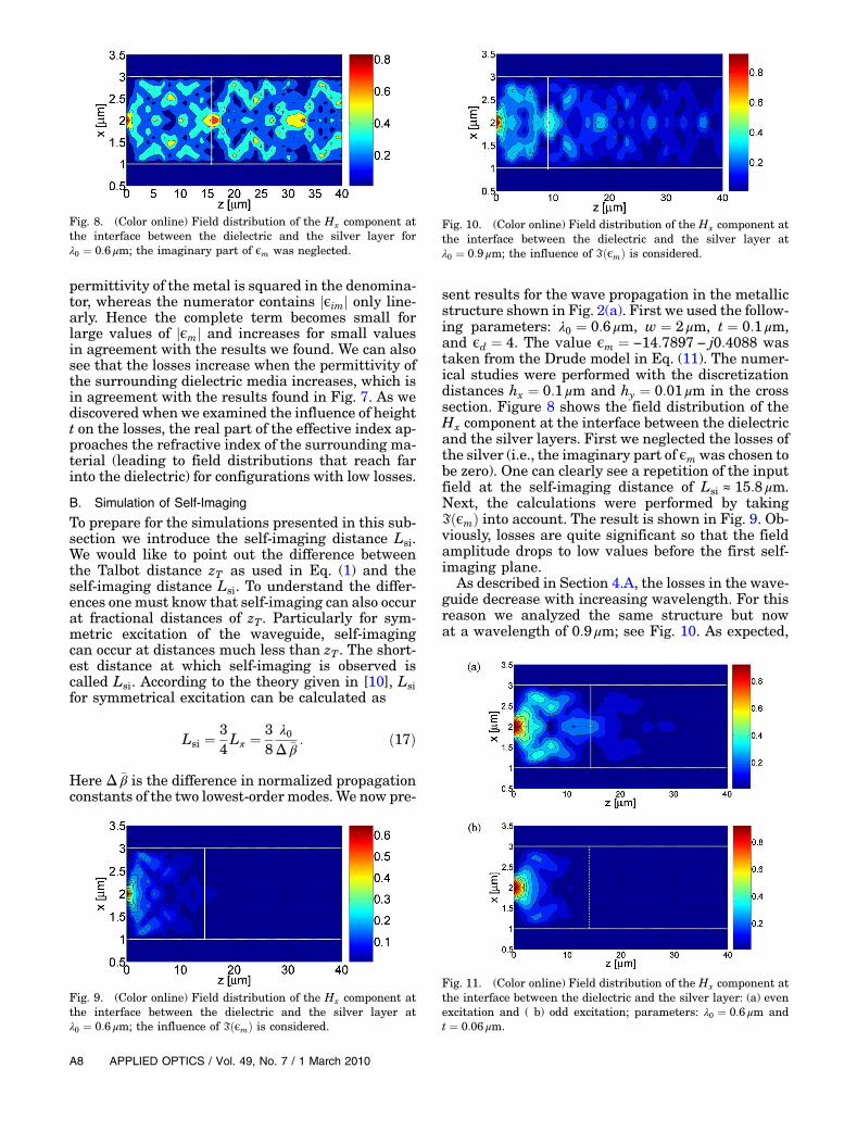
sent results for the wave propagation in the metallicstructure shown in Fig. 2(a). First we used the follow-ing parameters: λ0 ¼ 0:6 μm, w ¼ 2 μm, t ¼ 0:1 μm,and ϵd ¼ 4. The value ϵm ¼ −14:7897 − j0:4088 wastaken from the Drude model in Eq. (11). The numer-ical studies were performed with the discretizationdistances hx ¼ 0:1 μm and hy ¼ 0:01 μm in the crosssection. Figure 8 shows the field distribution of theHx component at the interface between the dielectricand the silver layers. First we neglected the losses ofthe silver (i.e., the imaginary part of ϵm was chosen tobe zero). One can clearly see a repetition of the inputfield at the self-imaging distance of Lsi ≈ 15:8 μm.Next, the calculations were performed by takingIðϵmÞ into account. The result is shown in Fig. 9. Ob-viously, losses are quite significant so that the fieldamplitude drops to low values before the first self-imaging plane.
As described in Section 4.A, the losses in the wave-guide decrease with increasing wavelength. For thisreason we analyzed the same structure but nowat a wavelength of 0:9 μm; see Fig. 10. As expected,
Fig. 8. (Color online) Field distribution of the Hx component atthe interface between the dielectric and the silver layer forλ0 ¼ 0:6 μm; the imaginary part of ϵm was neglected.
Fig. 9. (Color online) Field distribution of the Hx component atthe interface between the dielectric and the silver layer atλ0 ¼ 0:6 μm; the influence of IðϵmÞ is considered.
Fig. 10. (Color online) Field distribution of the Hx component atthe interface between the dielectric and the silver layer atλ0 ¼ 0:9 μm; the influence of IðϵmÞ is considered.
Fig. 11. (Color online) Field distribution of the Hx component atthe interface between the dielectric and the silver layer: (a) evenexcitation and ( b) odd excitation; parameters: λ0 ¼ 0:6 μm andt ¼ 0:06 μm.
A8 APPLIED OPTICS / Vol. 49, No. 7 / 1 March 2010

the decay of the field is more moderate and the self-imaging is more pronounced. Here it is important tonote that the self-imaging distance is shorter than inthe previous case. Although the wavelength occurs inthe numerator of Eq. (17), the self-imaging distancedecreases with λ0 because Δ �β in the denominator isessentially proportional to λ20. For λ0 ¼ 0:9 μm wefind Lsi ≈ 9:1 μm.From these considerations it becomes obvious that
operating at larger wavelengths is recommended be-cause of the lower attenuation of the field, at leastwith current devices. Figures 8 and 9 show field dis-tributions for even modes and Fig. 10 for odd modes.The results for the respective other cases (odd fieldsfor Figs. 8 and 9, even fields for Fig. 10) are not dis-played because the even and the odd fields look simi-lar in both cases. This is due to the large thickness ofthe metal layer, which, in agreement with the pre-vious analysis, leads to the degeneracy of even andodd modes (see Fig. 5). For comparison we examinea situation in which one can expect a significant dif-ference between even and odd modes. For our exam-ple we chose t ¼ 0:06 μm (see Fig. 5). The determinedfield distributions are shown in Fig. 11, which clearlyindicates the difference. To quantify these results wecompare the values for the losses from Fig. 5 withthose determined from the simulations of the wavepropagation. For the simulations the values forlosses were derived from the maxima at z ¼ 0 andz ¼ Lsi. For t ¼ 0:06 μm we calculated losses of 0.95(odd case) and 0.71 (even case). These values weredetermined from the field distributions according to
loss1 ¼ 1 − jHðz ¼ LsiÞj=jHðz ¼ 0Þj: ð18Þ
We can compare these values with the loss factor ofthe eigenmodes shown in Fig. 5, from which we ob-tained 0.93 (odd case) and 0.69 (even case). Herewe used
loss2 ¼ 1 − expf−�αk0Lsig: ð19Þ
Obviously, the numerical results are in good agree-ment. However, we must bear in mind that, in thefirst case [Eq. (18)], the complete field is determinedby the superposition of the different modes thatmight not be exactly in phase. For this reason in-equality loss1 ≥ loss2 holds.Finally, we take a look at the self-imaging dis-
tances Lsi. For this purpose we compare the valuesobtained with Eq. (17) with those of the simulation,i.e., visual inspection of Figs. 8–11. In the latter casewe looked for the maxima of the fields in the center ofthe waveguides. The results compiled in Table 1
show good agreement. Since the structure is lossy,the maximum field value depends on the interfer-ence of the modes and on their losses. Therefore,there are slight differences in the results obtainedwith Eq. (17). As one might expect, the best agree-ment is found between the MoL values and the onesfrom Eq. (17) when losses are neglected (t ¼ 0:1 μm,λ ¼ 0:6 μm). As one might also expect, Lsi is differentfor the even and odd fields for t ¼ 0:06 μm(λ ¼ 0:6 μm). For the odd modes the field decreasesto zero before self-imaging can occur, therefore wedid not assign a MoL value in Table 1 for this case.
5. Summary
We have examined the propagation of plasmonicwaves in metallic waveguides. In particular, we con-sidered self-imaging in plasmonic multimode wave-guides. The analysis of an effect well known fromclassical optics and also from conventional dielectricwaveguides lends itself to gain insight by drawingcomparisons. We began our analysis with a studyof the eigenmodes and examined the influence ofthe geometric waveguide parameters. This was donemainly with the purpose of investigating the at-tenuation properties of metallic waveguides. Wefound that losses can be reduced by decreasing thethickness of the waveguide, which in turn leads toan increased expansion of the field into the surround-ing medium. Therefore, one observes the existence ofa trade-off between loss and dimensional para-meters. Furthermore, dependency exists between at-tenuation and wavelength: for longer wavelengths,attenuation is lower and the devices become morepractical. Losses in plasmonic waveguides representa general problem that needs to be solved beforepractical applications can be considered.
For now we can conclude from our study that themethod of lines is capable of handling the materialcharacteristics of metal structures to simulate plas-mon wave propagation. The results obtained in thesimulations are in good agreement with analyticalpredictions. In future work, we wish to develop con-figurations in which the losses are reduced, whichmight be achieved by structuring the metallic wave-guides in a suitable manner. The use of exact simula-tion techniques can yield valuable results andinsights for the experimental realization of suchstructured plasmonic waveguides. This can be com-bined with considerations of coupling electromag-netic fields to metallic waveguides.
References1. H. Raether, Surface Plasmons, Vol. 111 of Springer Tracts in
Modern Physics (Springer-Verlag, 1988).
Table 1. Self-Imaging Distances Lsi Determined from the Field Distribution in Comparison with Eq. (17)
λ0 ¼ 0:6 μm (even) λ0 ¼ 0:6 μm (even) λ0 ¼ 0:9 μm (odd) λ0 ¼ 0:6 μm (even) λ0 ¼ 0:6 μm (odd)
t½μm� 0.1 [IðϵmÞ ¼ 0] 0.1 (lossy) 0.1 (lossy) 0.06 (lossy) 0.06 (lossy)Lsi½μm� (MoL) 15.8 14.5 9.1 15.0 (field ≈ 0)Lsi½μm� [Eq. (17)] 15.0 15.0 9.15 14.24 15.84
1 March 2010 / Vol. 49, No. 7 / APPLIED OPTICS A9

2. J. Ctyroky, J. Homola, P. Lambeck, S. Musa, H. Hoekstra,R. Harris, J. Wilkinson, B. Usievich, and N. Lyndin, “Theoryand modelling of optical waveguide sensors utilising 20 sur-face plasmon resonance,” Sens. Actuators B 54, 66–73(1999).
3. R. D. Harris and J. S. Wilkinson, “Waveguide surface plasmonresonance sensors,” Sens. Actuators B 29, 261–267(1995).
4. Z. Liu, J. M. Steele, W. Srituravanich, Y. Pikus, C. Sun, andX. Zhang, “Focusing surface plasmons with a plasmonic lens,”Nano. Lett. 5, 1726–1729 (2005).
5. Z. Liu, J. M. Steele, H. Lee, and X. Zhang, “Tuning the focus ofa plasmonic lens by the incident angle,” Appl. Phys. Lett. 88,171108 (2006).
6. M. R. Dennis, N. I. Zheludev, and F. J. G. de Abajo, “The plas-mon Talbot effect,” Opt. Express 15, 9692–9700 (2007).
7. R. Pregla and W. Pascher, “The method of lines,” in NumericalTechniques for Microwave andMillimeter Wave Passive Struc-tures, T. Itoh, ed. (Wiley, 1989), pp. 381–446.
8. R. Pregla, Analysis of Electromagnetic Fields and Waves: theMethod of Lines (Wiley, 2008).
9. O. Conradi, S. Helfert, and R. Pregla, “Comprehensive model-ing of vertical-cavity laser-diodes by the method of lines,”IEEE J. Quantum Electron. 37, 928–935 (2001).
10. L. B. Soldano and E. C. M. Pennings, “Optical multi-modeinterference devices based on self-imaging: principles andapplications,” J. Lightwave Technol. 13, 615–627(1995).
11. H. F. Talbot, “Facts relating to optical science, No. IV,” Philos.Mag. 9, 401–407 (1836).
12. A. W. Lohmann and D. A. Silva, “An interferometer based onthe talbot effect,” Opt. Commun. 2, 413–415 (1971).
13. J. Jahns, E. ElJoudi, D. Hagedorn, and S. Kinne, “Talbot in-terferometer as a time filter,” Optik (Jena) 112, 295–298 (2001).
14. O. Bryngdahl, “Image formation using self-imaging tech-niques,” J. Opt. Soc. Am. 63, 416–419 (1973).
15. R. Ulrich andG. Ankele, “Self-imaging in homogeneous planaroptical waveguides,” Appl. Phys. Lett. 27, 337–339(1975).
16. S. F. Helfert, B. Huneke, and J. Jahns, “Self-imaging effect inmultimode waveguides with longitudinal periodicity,” J. Eur.Opt. Soc. 4, 09031 (2009).
17. S. F. Helfert and R. Pregla, “The method of lines: a versatiletool for the analysis of waveguide structures,” Electromag-netics 22, 615–637 (2002),
18. R. Pregla and S. F. Helfert, “Modeling of microwave deviceswith the method of lines,” in Recent Research Developmentsin Microwave Theory and Techniques, B. Beker and Y. Chen,eds. (Research Signpost, 2002), pp. 145–196.
19. H. J. W. M. Hoekstra, P. V. Lambeck, G. J. M. Krijnen, J.Čtyroký, M. D. Minicis, C. Sibilia, O. Conradi, S. Helfert,and R. Pregla, “A cost 240 benchmark test for beam propaga-tion methods applied to an electrooptical modulator based onsurface plasmons,” J. Lightwave Technol. 16, 1921–1927(1998).
20. M. Besbes, J. Hugonin, P. Lalanne, S. van Haver, O. Janssen,A. Nugrowati, M. Xu, S. Pereira, H. Urbach, A. van de Nes, P.Bienstman, G. Granet, A. Moreau, S. Helfert, M. Sukharev, T.Seideman, F. I. Baida, , B. Guizal, and D. V. Labeke, “Numer-ical analysis of a slit-groove diffraction problem,” J. Eur. Opt.Soc. 2, 07022 (2007).
21. O. Conradi, S. Helfert, and R. Pregla, “Modification of the fi-nite difference scheme for efficient analysis of thin lossy metallayers in optical devices,” Opt. Quantum Electron. 30, 369–373 (1998).
22. J. Gerdes, “Bidirectional eigenmode propagation analysis ofoptical waveguides based on method of lines,” Electron. Lett.30, 550–551 (1994).
23. S. F. Helfert, A. Barcz, and R. Pregla, “Three-dimensional vec-torial analysis of waveguide structures with the method oflines,” Opt. Quantum Electron. 35, 381–394 (2003).
24. R. Pregla, “Novel FD-BPM for optical waveguide structureswith isotropic or anisotropic material,” in Proceedings of theEuropean Conference on Integrated Optics and Technical Ex-hibit (European Optical Society, 1999), pp. 55–58.
25. R. Pregla, “MoL-BPM method of lines based beam propaga-tion method,” in Methods for Modeling and Simulation ofGuided-Wave Optoelectronic Devices (PIER 11), W. P. Huang,ed. (EMW Publishing, 1995), pp. 51–102.
26. P. Berini, “Plasmon-polariton waves guided by thin lossymetal films of finite width: bound modes of symmetric struc-tures,” Phys. Rev. B 61, 10484–10503 (2000).
27. J. J. Burke, G. I. Stegeman, and T. Tamir, “Surface-polariton-like waves guided by thin, lossy metal films,” Phys. Rev. B 33,5186–5201 (1986).
A10 APPLIED OPTICS / Vol. 49, No. 7 / 1 March 2010


![Enhancing the Angular Sensitivity of Plasmonic Sensors ...biotheory.phys.cwru.edu/PDF/AOM.pdf · ultrasensitive plasmonic biosensors.[29,30] A plasmonic nanorod metamaterial (Type](https://img.pdfslide.net/doc/110x75/5fcdd2c6db367d06a677e7be/enhancing-the-angular-sensitivity-of-plasmonic-sensors-ultrasensitive-plasmonic.jpg)