Embed Size (px)
Citation preview

AND DE.VELOPMENT BRANCHe.. N4 -Mf::N 7 OF NATIONAL DEFENCE
C A N A { A
Li o D"FENCE RESEARCH
TABI IgaSHMEO OTTAWA
UREO TECHNICAL NOTE NO. 80-1.DFf7O TN 801
A PfMP uE SIP E U u iir DrvIEW OF
TRAVELL NG-WAVE TUBE TECHNOLOGY
byR. Luiz
L•Ji7-J
P; 'JECr NOi. NOVEMBER 1979OTTAWA
2 -58 75
CAUTION
~ This~~tt~r~ iifurr Irshei m.ih tip cypteIv. understandidngI tai U roppietarv and patent rtghtS will be protected.
L______

RESEARCH AND DEVELOPMENT BRANCHC? .
DEPARTMENT OF NATIONAL DEFENCE
CANADA
DEFENCE RESEARCH 'ESTABLISHMENT OTTAWA/TECHNICAL
jcj
A COMPREHENSIVE REVIEW OF TRAVELLING-WAVE TUBE TECHNOLOGY
Radar ESM SectionDefence Electronics Division
PROJECT NO.31 BOO

ABSTRACT
A review of TWT technology is presented comparing selected aspectsand design procedures relative to application.
The general theory of operation of various types of TWT designsis discussed together with a review of principles of their constructionand trade offs.
RSUHM
Une revue de la technologie des tubes A ondes progressives (TWT)est presentge, comparant certains aspects et procedures par rappart aux
applications.
La thgorie g~nirale d'opfration de plusieurs modales de tubes Aondes progressives 'est presentee, avec une revue des principes de fabrication
ainsi que des avantages et desavantages de chaque type.
By ftfIO
Di+ t r£ib•-L
B c vp
- - - i

TABLE OF CONTENTS
V: PAGE
ABSTRACT/RESUME .............................................. iii
TABLE OF CONTENTS ................. # ........................ . v
:; il1 .0 INTRODUCTION .. . . . . . . . . . . .1.. . .. . .
2.0 DESCRIPTION OF THE TWT .................. . ....... 1
3.0 BASIC OPERATION ............................................... 2
4.0 THE CHARACTERISTICS OF TWT'S AND VARIOUS CONFIGURATIONS ..... 2
4.1 The Gain, Bandwidth and Efficiency .................... 4
4.2 The $ever .......... ,.............................. ..... 5
4.3 Power and Perveance . .................... 64.4 Large Signal (Non-linear) Operation ................. 7
4.5 Noise ............. 8
4.6 Milli•eter-wave Tube .......... ....... ...... ....... 8
4.7 Backward-wave Amplifier ............... 9
4.8 Saturation ..... . . . . . . .. . . . . .............. 10
4.9 Dual Mode . ... .... .... 12
4.10 Modulation and Control ............... 12
4.11 The Crossed-field TWT ...... 13
5.0 SLOW-WAVE STRUCTURES .................... ...... . 14
5.1 Amplification Process ................ ............. 14
5.1.1 The Helix ..................... 14
5.2 111gh Power Limitations ................................ 16
"5.3 Other .elical Structures ................ ,............... 17
a) Twin Crosswound Helix ............. ............... 17
b) Sheath Helix #.b... 9..9....999 *.9...9.. 17

TABLE OF CONTENTS (CONTINUED)
PAGE
c) Tape Helix 1................. ........... ...... 18
d) ml Hei .............Ba e........... ..................... 18
e) Rig and Bar Contrawound Helix .................... 19
5.4 "Forbidden" Zones .... ....... ........... 19
5.5 Dielectric Loading .............. ........................ 19
5.6 Derived Structures ............. ................. 19
5.6.1 Folded Transmission Lines ........................... 20
5.7 Couled-cavity Structures ........ . .. ........... 20
6.0 THE ELECTRON BEAM SYSTEM ............................. ........ 22
6.1 Electron -uns ................ ............... 22
6.1.1 Lens Compensatod Guns ........... . 23
6.1.2 Anode Projection -I11er's Principle ........... 24
6.1.3 Imode-lip Gun (Mathias and King Version of MllerGun .. 24
6.1.4 Hollow Beam Gun ......... ...... 24
7.0 T W1E BEA AND TRE FOCUSING SYSTEM .............................. 25
7.1 BMgnetic Field Prallel to the Axis ....................... 257.2 Be m F cu in .... .... ... ...... 2
f 7.2.1. Uniforni Magnetic Field ..... ...... ........ ...... ... .. 27
f•i'}i 7.2.2 Periodic Pertiuient Magnet (PPM) Focusing ............ 28
7.2.3 Periodic Electrostatic Focusina (P ...0X........ 28
7.3 Collectors ....................................... 4...... 29
7.3.1 Depressed Potential Collectors ...................... 29
7.3.2 Methods of Cooling .................... ........ 30
vi

TABLE OF CONTENTS (CONTINUED)
PAGE
8.0 MATHEMATICAL FORMULATION OF TWT ................................ 30
8.1 Travelling-wave Tube Gain ........................ 36
8.2 The Effect of Space Charge ................................ 37
8.3 The Helix as a Spiral Slot Transmission Line .............. 38
I !i• ~~8.4 Phase Velocity and Group Velocity ................ 39
8.5 Coupled-cavity Structures - A Lumped Circuit Model ........ 41
8.6 Hollow Beams .................................. ........ 42
9.0 CONCLUDING REMARKS ............................................ 44
9.0 -FRNE .....hase..... Ve4iyadGopVlct .........
" FIGURE 1 -PORTION OF THE TRAVELING-WAVE AMPLIFIER PERTAINING TO
ELECTRONIC INTERACTION WITH RADIO-FREQUENCY FIELDS AND)RADIO-FREQUENCY GAIN ..................................... 51
FIGURE 2 - SCHEMATIC OF THE TRAVELING-WAVE AMPLIFIER ............... 51
FIGURE 3 - TWO-SECTION SEVERED TRAVELLING-WAVE TUBE ............ .... 52
FIGURE 4 -DIAGRAM SHOWING DIRECTIONS OF ELECTRON AND POWER FLOWFOR: (a) NORMAL TRAVELLING-WAVE TUBE (FORWARD WAVEAMPLIFIER); (b) BACKWARD) WAVY AMPLIFIER ................. 52
FIGURE 5-CROSSED-VIEID TWT ............... ......... ....... 53
FIGURE 6 SLOW WAVE lhULTRS~5SFIURE6 sLW WVESTRUC-TURES .................................... 53
FIGURE 7 -TWIN CROSSWOUND HELIX ........................ 53
FIGURE 8 -. SH9A_ H , ELIX . ............ .... ............... 54
FIGURE 9 TAPE HLLIX ............. 5.......... . 54
FIGURE 10 HELIX STRUCTURES .................... 55
FIGURE 1-SLOW AVE STRUCTURES ....... ** ...... *...*.... 5
FIGURE 12 - COUPLED CAVITY STRUCTURE (CRODOROW-NALOS STRUCTURE) ..... 57
iFIGURE 13 - L "HUGIIE" STRUCTURE ....... 57
vii

TABLE OF CONTENTS (CONTINUED)
PAGE
FIGURE 14 - THE "CENTIPEDE" STRUCTURE (COUPLING PLATE) .......... 57
FIGURE 15 ................................... 8........ 58
FIGURE 16 - PIERCE GUN ...................... .. ............... 58
FIGURE 17 - TWO ANODE LENS-COMPENSATED GUN .......................... 59
FIGURE 18 - GUN DESIGNED BY MATHIAS ACCORDING TO MULLER'S PRINCIPLE 59
FIGURE 19 - MATHIAS AND KING'S HIGH VOLTAGE VERSION OF MUILLER-TYPEGUN ... .. . . ............. .... ............. * * ..... tq 60
FIGURE 20 - PERSPECTIVE VIEW SHOWING PATHS OF OUTER ELECTRONS ....... 60
FIGURE 21 - A PRACTICAL ARRANGEMENT FOR LAUNCHING BRILLOUIN FLOW .... 61
FIGURE 22 - A PRACTICAL ARRANGEMENT FOR LAUNCHING SMOOTH FLOW ATFIELDS ABOVE BRILLOUIN ..... ..... .................. 61
* FIGURE 23 - ELECTRON GUN CONTROL ELECTRODES ...................... 62
"FIGURE 24- BOWING OF FIELD LINES ................................... 63
FIGURE 25 - C-MAGNET ................................ ..... 63
FIGURE 26 - SOLENOID WITH SEPARATE COILS AND IRON END PLATES ........ 63
FIGURE 27 - CYLINDRiWAL POT PE0MUNENT MAGNET . 64
FIGURE 28 - PPM-FOCUSIN6 STRUCTURE EMPLOYING AXIALLY 4AGNETIZEDRINGS ..... ............ .. ........ 64
--'AMXE 29 - PERIODIC FOCUSING BY CONVERGING MAGNETIC LENSES ......... 64
FIGURE 30 - iEPRESSED COLLECTOR T.W.T" ...................... ... 65
FIGURE 31 - A DEPRESSED COLLECTOR WHICH SUPPRESSES SECONDARY CURRFNT 65
FIGURE 32 - EQUIVALENT CIRCUITS ........................... ......... 66
FIGURE 33 - SPACE CHARGE EFFECT ........... 67
FIGURE, 34 ..... ............ .. .... * 67
FIGURE 35 - EQUIVALENT LUMPED CIRCUITS FOR TiLE COUPLED-CAVITY-STRUCTURE ...................................... 68
n• viii

I ~ ~TABLE OF CONTENTS (CONTINUED) PC
.. FIGURE 36 HOLLOW BEAM GUNS ..... . ......... 69
FIGURE 37 CROSS-SECTION OF HOLLOW BEAM . 69
iix
HIi
l l ... ii:• S] i fr. PAS
4 ix

// I
1.0 INTRODUCTION
The travelling-wave tube (TWT) was invented by R. Kompfner in 1943,and the principle of TWT amplification was demonstrated by him at BirminghamUniversity in the same year. A small signal theory of this devi.ce wasextensively developed by J.R. Pierce.
The TWT has been constructed to operate at many wavelengths, rangingfrom one meter to one millimetre. It has found wide application primarilybecause at any given frequency or power level, it offers much more bandwidth
Srthan any of its competitors.
The travelling-wave tube, though structurally simple, is a *Con-structed Complication*. Because of its structural simplicity, TWTs havebeen built to operate at frequencies as high as 50 GHz. Modern require-ments for TWr amplifiers often call for very wide bandwidths combined withhigh power output.
For any practical application an ideal WIT is seldom available as an#oef-the-shelfV item mainly because more than two dozen Independent parametersare required in order to completely describe the tube.
--.ith the introduction of the 4T two chief limitations of Magnetronsand Klysvrons, naely, their narrow: bandwidth and s1iw :v.i.g capabilities,
were largely overcoue. The field of Electronic Counter Measures (ECM) hasimmensoly benefited from the uniqua capabilities of the TWT.
The T1' is onq of the thoroughly researched technologies. Thezefore,appropriate references should be consulted if the reader i1 interested in
ji : • further dutails on any of the topics described In this report. Severalreferences used in the preparation of this report are listed.
2.0 DESCRIPTION OF THV TWT
The W1JT is a device to transker energy from a stream of electron6 toan alternating, radio frequency, current, (Figure 1). Unlike Klystrons and,agnetrons which depend upon standinugwaves to produce the high frequencyfxolds with which the beam Interacts locally, the TWT makeb use of the princ-iple of a distributed Interaction mechanium between the electron beam and thetravelling electromanettc waves. Referring to Figure 2, the T1T consists ofa Gun assembly (hpater, cathode and ',ode) which produces a stream of electronscalled an electron beam, a beam focussing system which produces sufficientlongitudinal magnetic field to keep the electron beam from spreading, acollector to absorb the spent beam, a cooling system to help dissipateexcess heat and a helix through which the electron beam passes before beingabsorbed by the collector.

2
3.0 BASIC OPERATION
Referring j Figure 2, at the input the wave is transferred from awave guide to the helix by means of a short antenna and, similarly, at theoutput the wave is transferred from the helix to a short antenna from whichit is radiated into the output wave guide. The purpose of the helix is toslow down electromagnetic wave which is travelling, nominally, at the speedof li,ýht, to some required velocity. The signal amplification of a TWT iscreated from the interaction between the electron beam and the electromagneticwave travelling through the helix. The amplification is most effective whenthe speed of the electrons in the beam and the speed of the travelling waveare about equal. For example, the speed of electrons produced by a beamvoltage of 1500V is about 1/13 of the speed of light. Therefore, in orderto slow down the electromagnetic wave travelling at the nominal speed oflight, a helix made of a wire of length 13 times the length of the helixitself is required.
The helix, in the absence of the electron stream, supports the pro-pagation of a wave with an axial electric field and such a wave may travel ineither direction. It is found that in the presence of the electron beam thewave travelling against the electron motion is little affected, but the wavetrawvllina in the d,.rectioli of electron motion is broken up into threecomponents. For a lossless helix one of these forward waves is attenuated,one is unattenuated, and the third iucreases in amplitude as it travels (orexperiences uegative attenuation). On the average, the electronS travel a
-* :little faster than the amplified wave.
As the electrons move in synchronism with the at'plified wave, theybecome bunched. I _ese bunches, while moving rapidly in opposing field regions
* •of the helix, give up energy to. the field. For a given electromagnetic energytravelling doun the helix, the stronger the field that acts on the electrons,the more the bunching and the more energy the bunches give up to produce
greater signal amplification. It is found that 4s the frequency is increasedthe EM wave tonds to cling close to the helix such that the electric fieldintensity decreases near the axia of electron flow. Eor this reason the gaintends to decrease as the frequency increases because the field is constrdinedcloser to the helix. At very low frequencies the helix will be only a fewwavelengths long and therefore the gain is low at very low frequencies. We
j. thus obtain a broad gain taxim=m with respect to frequency.
(i~ "4.0 THE CHARACTERISTICS OF 1VT'S AND VARIOUS CONFIGUMtTIONS
Two basic types of slow-wave structures (or circuits) have receivedconsiderable attention as the interaction structures for travelling-wave tubes.These are the helix and the periodically-loaded wave guide, which is a bad.-pass microwavo. filter.

1 3
i The helix has many advantages when used as a travelling-wavepropagation structure. It is by nature a broad band device to which itis relatively easy to couple over a wide frequency range. Attenuationmay easily be added at various places along the helix to prevent the tube
S'from oscillating when used as an amplifier.
However, high power requirements coupled with broad bandwidthpersuaded scientists to design many modified forms of helices, each onespecifically suited for a particular application. In spite of all these,pulse operated power tubes requiring outputs of several megawatts, withduty cycle ranging from a fraction of a percent to several percents, wererequired. However, the voltage handling limitation of the helices wasfound to be 10 KV giving a peak RF power output of a few kilowatts. Beyondthat, the pitch of the helix became coarse and the RF coupling to the beam"became very poor,
Therefore, loaded wave guides or transmission lines found increasingapplication as circuits for TWTs. These structures are filter type circuitsconsistins of wave guides with periodic loading to slow the wave velocity tothat of Lhe electrons in the beam. They have advantages over the helix-typestructure by being much more rugged and are capable of dissipating much largeramounts of heat, because the entire structure is bade out of metal that can beeasily cooled. These coupled-cavity circuits are the fundamental buildingblocks of an extremely importauL clabs of high-power WTs. The versatility ofthe coupled-cavity circuit i6 demonstrated by the fact hit it is widely usedfrom L-band to millimeter waves and for power levels from 1-500 KW.
Though helix and coupled cavity circuits are two different structuresto meet the same requiremeurs, there are some distinguishing differencesbe tweon thea.
"One logical criterion for a high gain circuit is its impedance valid,* given by
4 (1)
:4where E = is; the peak axial field strength
=P is the power flowing in the helix. is the phase constant and is de'ined by where w is the
radian frequency and v is tie velocity of the wave.
One way to make ZO large is to decrease Ohe power, which is afunction of stored energy for a given field strength. In an eloetromagneti:""ave, half of the stored energy is electric and half is magnetic. Thus,to make the total stored energy for a given field g trength small, we must
amplifier the phase velocity must be constant; that is, 8 must be proportional"to the frequency, Therefore, two desirable circuit properties for high gainare high impedance and constant phase velocity.
I IM
4
4.1 Gain, Bandwidth and Efficiency
The principal factors which causes the gain to vary with frequencyare: 1) variation in the velocity of the wave on the circuit with whichthe beam interacts; 2) variation in the effective length of the tube inwavelengths; 3) variation in the strength of the axial electric fieldinteracting with the beam; 4) variation of the impedance match at the
* input and output transducers, and at the attenuator.
The effect of increasing the beam thickness on the gain vs. frequencycharacteristic of the forward wave amplifier is to increase the frequency atwhich the gain is a maximum, for a given beam radius, and to increase the
* _ I bardwidth.
The gain of a travelling-wave tube is proportional to the number ofwavelengths in the tube at the electron velocity. The gain per wavelength isincreased by increasing the beam perveance, and the wavelength is decreasedas the voltage is decreased.
The physical size of a travelling-wave tube tends to be inverselyproportional to the centre frequency. As the frequency is decreased, itbecomes a major design problem to keep the tube size from becoming too large.
Coupled-cavity TWTs are used for applications for which Klystrons"have insufficient bandwidth. These applications include communication systemsrequiring multiple carrier operation, radar applications, and electroniccounter measures (ECM). Coupled-cavity TWTs are used in these systems asthe output amplifiers and sometimes as drivers for crossed-field amplifiers.
Coupled-cavity TWT interaction is similar to helix TWT interactionin one respect, that is, power flows along the circuit. Coupling betweeni adjacent cavities is introduced to obtain increased bandwidth. (Couplingis achieved by means of slots or loops in the cavity end walls.) The cavities
are normally highly over-coupled, resulting in a bandpass-filter type ofcharacteristic. One of the important functions in coupled-cavity TWT inter-I action is the phase change occurring between cavities as a function offrequency. A decreasing phase characteristic is obtained if the mutualinductance of the coupling clot is positive, and un increasing phasecharacteristic is obtained for negative mutual inductive coupling of the
I • slot.
The electron bean interacts with a component of the circuit fieldthat has an increasing phase characteristic with frequency. Because of theperiodicity of the coupled-cavity circuit, the electric and magnetic fieldscan b- exprecsed mathematically in terms of a Fourier expansion. Therefore,the circuit periodicity can give rise to field components. For the circuithaving positive mutual inductive coupling between cavities, the electron beamtvelocity is adjusted to be approximately equal to the phase velocity of the
q, first forard-wave space harmonic. For the circuits employing negative mutualinductive coupling, the fundamental component of the circuit wave is suitablefor synchronism with the electron beam. Examples of ccupled-cavity TWT

circuits having fundamentally forward wave chF:act!'rlstic, and hence negativemutual inductive coupling, are clover leaf and centipede c.rcuits. Examplesof circuits having positive mutual coupling !:etwe:.-n cavities ai'e spaceharmonic and long-slot circuits.
¶ iiOptimum interaction characteristics are obtained by proper design ofthe cavity geometry. The cavity resonant frequency in the absence of magneticcoupling determines the high frequency cut-off of the interaction mode. Thecoupling slot in turn determines the amount of bandwidth in the interactionmode and interaction impedance is determined primarily by the cavity heightand by the gap and tube geometry.
Coupled-cavity TWTs are constructed with a limited amount of gainper section of cavities to ensure stability. Each cavity section is terminatedat each end, either into a matched load or the input or output line, in orderto reduce the gain variations with frequency. The sections are normally"severed" with coupling between sections only through the electron beaminteraction, and with negligible amount of RF leakage through the beam hole.Cavity sections are cascaded to obtain higher tube gains than can be toleratedin one section of cavities producing stable gain greater than 60 dB over about30 percent bandwidth.
The gain of a zoupled-cavity tube is quite sensitive to the beamvelocity. In designing the tube, the beam voltage and cavity period aretypically adjusted to give a flat gain characteristic with frequency. Thisadjustment does not necessarily give the best power transfer to the circuitat the tube output. Therefore, some further adjustments in beam velocity orcircuit periodicity are required at the output end of the TWT. Typically,this adjustment has been made hy reducing the period of the last few cavities(taper) to improve the energy exchange. Alternatively, beam voltage can beincreased near the tube output, also resulting in a similar improvement intube efficiency. Also, an improvement in efficiency can be obtained in helixTWTs by increasing the circuit period in an appropriate manner.
.ii The overall efficiency of the tube is determined by the amount ofenergy converted to RF energy relative to that dissipated by the collector.Overall efficiencies of 20 to 55 percent have been obtained, including theenergy recovered by collector depression.
Another factor affecting the design of coupled-cavity TWTs is thetube stability, where oscillations can be predicted from the calculation ofgain. The most severe oscillation problem occurs when the beam is approximately
synchronous with the band edge frequency. This corresponds to the "Tr" phaseshift-per-cavity frequency for clover leaf circuits and to the "2 it" phase
J shift-per-cavity frequency for space harmonic circuits.
4.2 The Sever
The simple TWT has one serious disadvantage because of a possiblefeedback path from output to Input by way of the slow wave structure. Anypower reflected at a mismatch on the oitput terminal travels back down thestructure and, as there is usutlly a mismatch at the input, is reflected

6
again to give a feedback signal. Whenever the amplitude of this signal risesabove a certain value and its phase is such as to give positive feedback thetube bursts into oscillation.
It might be argued that it should be possible to adjust the phase ofthe reflected signal so that the feedback is always negative. Unfortunatelyin a wide band amplifier containing a large number of wavelengths between
* input and output there is always likely to some frequency at which there issufficient gain to cause oscillations. This situation is further complicatedby the fact that reflections at the input and output may well reverse theirsigns over the frequency range. Therefore, some sort of non-reciprocalelement which inserts loss only into the feedback path may he used. Onemethod of introducing a non-reciprocal element is to sever the slow wavestructure as shown in Figure 3, where each end of the break is terminated ina matched load. For fairly low average power operation lossy buttons may beplaced internal to the cavity structure. For higher average powers, circuitmatches are made by wave guides (or coaxial lines) which are then terminatedin resistive loads. Wave guide water load terminations are especially goodfor very high power tubes if the water is used as the coolant medium. Watercoolant is accomplished by inserting a hollow ceramic cylinder across asection of wave guide and water is passed through the ceramic cylinder. Thewater acts as the lossy medium in which the RF power is dissipated.
4.3 Fower and Perveance
"When discussing the power capability of TWTs it is important tomake a clear distinction between the peak and average power since thesetwo are limited by totally different considerations. The average power ata given frequency is almost always limited by thermal considerationsrelative to the RF propagating circuit. The electron beam focusing isnever perfect, and a elzable fraction of the total beam power is interceptedby the RF circuit. At some point the circuit temperature may approach themelting point of copper or the Curie temperature of iron in the case of areriodic Perwanedt •ondct (PPM) IN In both cases the tube is close to
which the TWT is designed. The beam current varies as the 3/2 power of thevoltage, that is
F0 K V0 (2)
ýihere.
Io is the beam current
Vo is the beam veltage
K, =is a constant kniown as perveance

7
The beam power, PB' is given by
P = 10V°B
5/2K V0 (3)
Perveance is a function of gun geometry only and does not dependon absolute dimensions. It is generally limited to a value not much greaterthan 2 x 10⁻⁶ (MKS) and most existing TWTs utilize a value between 1 or2 x 10 Once the perveance is fixed, the required voltage for a givenpeak power may be determined.
It will be noted that if the voltage is increased, the peak andaverage power capabilities increase considerably. This variation is adirect consequences of the way in which the circuit dimensions are selected.Large circuits will accommodate larger amounts of thermal dissipation, andhigher beam power will pernit more peak RF power. At some point the peakRF power will be limited by wave guide arcing problems and voltage breakdownin the electron - gun region.
In general. for very large percentage bandwidths, the averagepouar capaoili- may have to be reduced as much as 50 Percent.
4.4 Large Signal (N-n-linear) Operation
For small signal (lineaz:) analysis one of the assumptions made isthat the spa,e charge forces oetween electrons are negligible. However,under large signal cotnditions, the space charge field is not negligiole,and in some cases may eve. be much greater than the circuit field.
The large signal behaviour of the 1r4T is difficult to predict.Any adequate theory requitls a detailed non-linear analysis which is bothtime consuming and expensive without assurarce that all important factorssuch as space Qharge, coupling par.me"ir, loss etc., can be includedcorrectly.
M1ost TWT app.iicatioue require operation well izito the non-linearregion of the amplifier. At large signal level the gain iu reducedapproximately 4 to 6 d8 in compari±on to small signal gaft. The effectof operation near saturation (maxim- possible power output) for single-frequency input is to reduce the effect of change in input power on tbipoutr output or to reduce the ampiit'id changes as a function of freq,.&ucy,compared to the small-signal amplitude response.
Operation at large-signal levels produces harmonic outputN thatare typically 30 dD below the fundamental. The phase response doer, notdeteriorate at large signals as does the dmplitude response ann at a singleinput frequency the phase increases as the input power is increased. Thishappens because the beam slows down as energy is exchuaged with the RF wave.
42!. .

8
A measure of this phase change with drive power is called the AM to PMconversion coefficient. Also, intermodulation is produced as a result oflarge signal effects and this will add noise in the frequency band ofoperation.
In large signal operation the field along the slow-wave structureis composed of an infinite number of components orthogonal to one another.Phase velocities of the space-harmonic fields are lower than those of thefundamental field. The electron beam will interact appreciably only withthe fundamental field since the beam is approximately in synchronism withthe phase velocity of the fundamental field. Consequently, the space-harmonic fields in a helix may carry power along the slow-wave structurebut not contribute to the gain of the amplifier. The presence of space-harmonic fields lowers the actual helix impedance.
4.5 Noise
The noise figure of an amplifier is defined as the ratio of thetotal available noise output power to that part of the total available noisepower output which is due solely to the noise generated by the source. Thesource of noise is due to thermal noise (Boltzman) which may not be solelydependent upon the noise temperature of the source, for eaample, when anantenna is connected to the input.
Sources of noise are: 1) from streams of electrons emitted froma temperature limited cathode (shot noise); 2) thermal noise due to tempera-ture; 3) noise generated b1.y 'he grid% of the gun system (partition noise);4) pressure; 5) anode-helix sepa-ation; 6) degrees of space charge inthe gun; 7) power supply ripple modulation of tube electrodes.
In practice the noise figure may be reduced if:
1. The electrons are not allowed to be inter-cepted by other electrodes (less numberof electrodes).
2. The beam current is constant over the beamlength.
3. A strong magnetic focusing field is appliedso that electrons cannot vmove transversely.
4.6 Millimeter-wave Tube
i I iThe TWT interaction takes place when the electron velocity is equaito the phase velocity of the wave. However, if the electron velocity is very
ý_J much slower than the phase velocity of the wave, the interaction can stilltake place between the electrons and the first harmonic of the electro-magnetic wave. In operating the amplifier in this harmonic mode rather than

9
Sthe fundamental, the electron speed is reduced by a factor (27 + 8), (theAi 2 Trd 0hghsbeam voltage by the square of this factor) where 0 -- h-a dis-
placement between centre of adjacent slots separated by a distance d, andX is the wavelength in the structure.
For higher order spatial harmonics the reduction factor in theelectron speed is given by (2wn+6). However, there is little or no
0practical advantage in ex-ending the principle of spatial harmonic beyondn = 1, since this would not lead to wider resonator slots for any givenvoltage.
In general, millimeter wave tubes utilize very low perveanceelectron guns which create some unusual electron beam focusing problemsassociated with the proper containment of the "thermal" electrons. Hence,millimeter-wave tubes have frequently been equipped with heavy solenoids.Aside from the focusing structure, the major challenge in the manufactureof millimeter-wave tube is the precision and tight tolerances required forextremely small and fragile circuit parts.
4.7 Backward-wave Amplifier
As explained earlier it is possible for the electron beam to causethe signal to build up along the structure in a direction opposite to themovement of electrons. The power flow and the electron flow are then inopposite directions, as shown in Figure 4. Therefore, backward amplifica-tion is possible. This is not a broad band phenomenon as in a normal TWT,for at any given beam voltage there is only a narrow band of frequenciets overwhich there is substantial gain. The backward wave is inherently regenerativedue to the fact that the beam interacts with oppositely directed group andphase velocities.
An important property of backward waves is that the phase velocityis a strongly-varying function of frequency. Therefore, for a given beamvelocity, interaction can take place only over a narrow band of frequencies,and for a fairly weak interaction, the device acts as a narrow-band regenera-tLive amplifier. Since the frequency at which this interaction takes placedepends on the electron velucity, the amplifier can be continuously tuned infrequency by changing the beam voltage.
A careful analysis will show that as the beam loses energy to thewave, the wave tends to grow in amplitude. Since the backward wave, withwhich the beam is interacting, carrieb power in a direction opposite to themotion of the beam, the effect is for the wave to grow towards the gun endof the tube. This causes even stronger bunching of electrons, and theresult is a built-in feedback of a regenerative nature. For a given
9 ,physical length of the tube there is a critical beam current, called the"Starting Current" above which the regeneration is strong enough to causethe tube to oscillate at certain frequencies. Below the starting current,a signal which is introduced at the input (collector end of the tube) willbe aqplified if its frequency is near this value. As with all regenerative
iIn---- -,•-

10
amplifiers, the gain can be very large, but is critically dependent on beamcurrent and signal frequency.
The large signal calculations for backward-wave interactionincluding space-charge effects may be compared with small signal analysisas follows:
1. At small-signal levels, the phase velocity of thecircuit wave is unaffected by the presence ofthe electron beam even when space-charge effectsare included. At large signal levels, the phasevelocity of the circuit wave is only slightlyaltered by the presence of the beam.
2. The starting current of the backward-waveoscillator decreases initially with anincrease in the output voltage amplitudewhen space charge effects are small.When these effects are large, the startingcurrent increases at all times for anincrease in the output amplitude.
3. The large signal gain of the backward-waveamplifier decreases with an increase in
r. space charge effects.
4. A major part of the current is collected ona very short section of the circuit. Thislimits the average power capabilities of thecrossed-field devices since a sta)rt sectionof the circuit must dissipate most of the
j beam power.
5. The individual electron trajectories atlarge signal levels differ appreciablywhen cases in which space charge effectshave been included are compared withsimilar cases in which space charge
effects are neglected. The shape ofthe bunched beam is not significantlychanged.
4.8 Saturation
As the phase lag between the alternating component of the beam
current and the field increases, currents which normally interact with thefield to deliver power to the circuit eventually come into phase vnerethey substract power from the circuit. When this happens, the power onthe circuit begins to fall and the tube is said to be saturated. Themaximum power is obtained at this point and it is useless to allow inter-M.:ton to continue beyond this condition.

The actual amount of power that can be extracted from the beamdepends to what extent the bunches can be slowed down before saturation.The efficiency of the tube improves as the beam velocity is increasedabove the synchronous value. However, there is a limit to this process.If the beam velocity is made too high the gain falls off and eventuallyamplification drops. la~ general the beam velocity which gives maximumefficiency is higher than that which gives maximum gain.
Retardation in the phase of beam current is not the only factorcausing saturation. The bunches, being a transient phenomena, haveappreciable electron velocity spread which contributes to their destruction
* I before any useful energy transfer is completed. Space charge forces alsocause a debunching effect which must be taken into account.
As explained above, saturation is to some extent due to thereduction in beam velocity caused by the overall transfer of kineticenergy from the electrons to the field. This suggests that the efficiencycould be improved if the circuit was modified so that the phase velocityof the circuit wave also decreased toward the output end of the tube.Then, even though the bunches lose energy to the field and are thereforeslowed down, they still keep in "step" with the field and continue todeliver power to the wave. This is called "velocity tapering". inaddition to increasing efficiency, velocity tapering has another importanteffect, that is, the beam voltage at which maximum gain and maximumefficiency occur become the same. In an untapered tube, particularilyone in which space charge forces are relatively low, the beam voltage whichproduces the best efficiency is greater than that which produces the highestgain. If the taper is designed correctly these two voltages can be madethe same, particularily in those tubes which employ highly dispersive slowwave structures.
To look at the velocity tapering another way, at the output end of.. V the tube, where the majority of the power transfer from the beam to the wave
takes place, It is desirable that the bunches should be in the maximumdecelerating field so that the beam current and the wave are in phase andthe power transfer between them is maximum. This can be done by increasingthe beam velocity to exceed the phase velocity of the wave. However, thenthe bunching process suffers and gain falls off. The best bunching occurswhen the beam is near synachronism with the circuit wave, but then thephase of the beam current is incorrect for power transfer.
Tapering provides one method for improving the power factor,however, it is advantageous only when space charge forcea are relativelylow. AS Lhe space charge increases the beam voltage for maximum gainalso Increases and becomes more nearly equal to that which gives maximumefficiency. Again, with large space charge, debunching tends to destroythe bunches before there is any question of them becoming "out of step"with the circuit field, due to loss of kinetic energy.

12
4.9 Dual Mode
A subject of serious concern to the ECM systems engineer is a dualmode TWT. The purpose of such a device is to provide two different powerlevels in a single amplifier with no major changes and with good efficiencyfor both conditions. Typically the higher power level is the pulsed modewith duty cycle requirement of 10 percent or less, and the lower power modeis CW for noise, barrage, jamming. The higher pulsed power can be accommoda-ted by merely pulsing the grid of the electron gun with a positive signal toincrease the beam current and thus the beam power. Since grid modulationcan be accomplished with a relatively simple, compact, solid-state circuit,the system is quite flexible in meeting different types of radar threats withonly one output TWT.
If two separate TWTs are employed rather than one, the flexibilityand performance parameters can be somewhat improved. The driver is normallya CW tube, which must be more powerful than in the conventional system toovercome the insertion loss of the output tube. The overall efficiency ofsuch a chain can be made very significant.
4.10 Modulation and Control
Amplitude or phase modulation can be produced in a travelling-waveamplifier by uppcupriate variation of the beam current or beam voltage.This property makes possible a number of attractive master-oscillator andpower-amplifier applications.
Ampl i t ude modulation results when the beam current is varied, usuallyby means of a control grid in the gun, while a constant signal level is appliedat the input. Incidental phase modulation is also produced in this case, andthus the method may be limited to those applications where the RF phase isrelatively unimportant.
Phase modulation occurs when the helix voltage changes, because ofthe change in the velocity of the beam as a function of the number of wave-lengths along the tube, Since the gain of the tube depends rather criticallyon synchronism between the wave and the beam, the helix voltage can bechanged only by a small amount before incidental amplitude modulationbecomes serious.
A wide variety of combinations of amplitude and phase modulationis possible with a TNT, which allows the synthesis of practically any kindof microwave spectral distribution within the bandwidth limitations of thetube and its modulating electrodes. For example, balanced or suppressed-carrier modulation can be accomplished by amplitude-modulating with a full-wave-rectified signal, and simultaneously reversing the phase with a square-wave version of the signal applied to the helix.

13
Thus, the travelling-wave amplifier is an extremely flexible devicefor producing a wide range of different kinds of microwave signals, and iscapable of accomplishing this over a large frequency range without the needfor any mechanical tuning adjustments.
4.11 The Crossed-field TWT
The fundamental distinction between a crossed-field travelling-wavetube and the normal TWT lies in the arrangement of the steady electric andmagnetic fields used to form and maintain the electron beam.
"In a normal TWT the electrons are drawn from the cathode and are"accelerated to the correct velocity by a steady, axial, electric field inthe gun region. Subsequent beam spreading is prevented by applying an axialmagnetic field. All this field does is to inhibit transverse motions of theelectrons; it does not play any major part in the RF process. As long as itis of adequate strength to keep the transverse motions within the beam tunnel,its value is not critical.
In the crossed-field TWT Figure 5, the steady electric field isapplied between two parallel electrodes, one of which is the slow wavestructure. The magnetic field is applied in a direction perpendicular tothe electric field. If the electrons are injected into this system withcorrect velocity they move in a straight line perpendicular to both electricand magnetic fields.
Although the crossed-field NIT also involves interaction betweentravelling waves and electrons moving at nearly the same velocity, itdiffers from the ordinary TWT in two principal ways. First, the meansfor focusing the beam uses an adjustment between crossed electric andmagnetic fields. Second, the electron's loss of energy to RF fields is
accomplished by the extraction of potential energy from the static electricfield as the electrons propagate in the circuit. Thus, the interaction
process does not extract net kinetic energy from the beam; thn electronsstay in synchronism with the circuit wave to convert large amounts ofpotential energy into RF energy. For this reason crossed-field TWTsprovide high efficiency. Power capacities of these tubes may be increasedby operating at higher voltages, by improving the interaction efficiency,or by increasing the beam current.
The crossed-field arrangement has the practical advantage ofproviding a much more convenient magnetic field configuration. Becausethe magnetic field has only to be applied across the width of the tube,"the air gap in the magnet is considerably less than in the case of anordinary TWT. Therefore, less magneto-motive force is necessary and this1 often results in a considerable saving of weight, particularily whenpermanent magnets are used.
However, crossed-field systems have some drawbacks. One is that,if the high efficiency is to be realized, the slow wave structure is likelyto receive much more intense electron bombardment than in an ordinary TWT,and this imposes limitations on its average power-handling capacity. Also

14
there is a very high noise content in the output of crossed-field TWTs andthere are severe difficulties in preventing feedback and obtaining stablegain operation.
5.0 SLOW-WAVE STRUCTURES
The following sections discuss design considerations for thedevelopment of slow-wave structures for TWT applications.
5.1 Amplification Process
Travelling-wave amplification takes place when the electron velocityis approximately equal to the phase velocity of the travelling electro-magnetic wave. In practice, electron velocities range from about two-thirdsthe velocity of light, in very high power tubes, to about one-tenth thevelocity of light, in low power tubes. On the other hand, the phasevelocities of an electromagnetic wave !upported by normal transmission linesare usually either equal to or greater than the speed of light. Therefore,in order to make use of the property of travelling-wave amplification meansmust be provided to slow the propagating electromagnetic waves down to aspeed equal to the velocity of electrons in the beam. It is for thissituation that the use of slow-wave circuits or slow-wave structures
5becomes important. The purpose of a slow-wave structure is, therefore, toslow down the propagating electromagnetic wave to velocities correspondingto the electron beam velocity.
A wide variety of slow-wave structures are available; a few ofthese which have found practical application will be considered here.
As shown in Figure 6, slow-wave structures may be divided into two
distinct groups, namely, uniform structures, like the helix, and periodicstructures with filter-like properties such as the coupled-cavity arrange-ments.
5.1.1 The Helix
A "loaded" transmission line such as a helix is the simplest slow-wave circuit. To a first approximation the helix can be regarded as aspiral slot transmission line around which the energy propagates atapproximately the velocity of light. When an electromagnetic wave ismade to propagate down the helix, the fringing field adds up to give alongitudinal travelling field along the axis, expressed by,
---!
15
i =E E sin W(T-) (4)
where,
E = the longitudinal electric field
w• = the radio frequency
z = the axial distance along the helix
pV the phase velocity of the axial field
V c sinp
and.
Sthe pitch of the helix
This approximation is only valid over the range of about four turns
per wavelength. When a large number of turns per wavelength are used themetal between the slots tend to short out the current associated with theadjacent slots, and this will alter the propagation contants, For a helicalslow-wave structure, if the frequency is not too low, the RF wave travelsessentially along the wire at the velocity of the light, so that thecomponents of its velocity along the axis of the helix is reduced byapproximately the helix pitch, P, to the helix circumference. The fieldsinside and outside can be found by solving KXWLLt.'s equations.
The helix is often used as a slow wave propagating circuit in aTWT, because it is easy to construct and it can propuaate a vide-band, non-dispersive# forward wave which has relatively high Impedance. Based on theoryand measurement the helix is far superior to any other type of propagatingstructure. The low power helix TWT is still the 'king of bandwidth' becauseit provides virtuailly constant phase velocity at all frequencies. The helixtype Th'Ts hove bandwidths tit excess of an octnve. Since the helix geometrydoes not involve large metallic surfaces, the stored energy for a givenpower level, as compared to other structures, is very low. It can producemaximum axial electric field in the region of the electron beam and it canmaintain constant phase velocity (no dispersion). The helix also possesses
a very manageable made structure which is another reason for its superiorityover other structures. Because of its natural uniformity it can provide astrong interaction between the electric field and the beam. This phenomenonis referred to as the circuit impedance even though it relates to the electricfield which is available for interaction with the electron beam and is notthe same impedance generally employed in ordinary microwave circuits. Relixtype TWTs are quite capable of delivering several kilowatts of CW power atS-band and C-band over an octave of frequency coverage.

16
J Aside from purely electrical considerations, the helix is an idealstructure from the mechanical standpoint because of its simple and precisefabrication and it can be accurately assembled in structures with minimumcost.
5.2 High Power Limitations
A helix cannot be designed to work with high voltage electron beamswhich is necessary for high power. The electron velocities at high voltagesare very damaging for the helix, because as the helix pitch becomes coarsethe RF coupling to the beam becomes poor. Therefore, the limit of helixTWTs is about 10 KV and a peak RF power output of a few kilowatts. Also athigher power levels, the bandpass characteristics of helix slow-wavestructures leads to band-edge oscillation problems. Furthermore, bothforward and backward waves ma; propagate on the RF structure, leading tothe possibility of backward-wave oscillations. In order to avoid backward-wave oscillations it is necessary that the operating point of the TWTs be"set around 4 turns/wavelength.
Although the helix TWT is a broad band device its relatively lowpov.er output may be explained as follows, In order to increase the poweroutput, beam power must be increased. In order to maintain the powerdensity in the beam at reasonable levels it is necessary to increase beamdiameter which requires an increase in helix diameter. At high voltagesthe increased helix diameter is advantageous as far as the interactionbetween the beam and the travelling-waves are concerned. However, theincreased diameter maikes the helix an open structure and the increasedvelocity of electrons causes the space-charge to build up. Then theefficiency and the fundamental helix impedance will be greatly reducedand the tendency toward backward-wave oscillation increases considerably.Thus the only alternative (with a single helix) is to return to smallerhelix diameters and higher power densities in the beam. Because of itslimited cooling possibilities the helix is limited in the amount of powerit can dissipate.
Another important practical limit is the value of the axial magneticfield required to confine the electron flow to exactly axial directions.There comes a point when this field is so high that the magnetic systemneeded to provide the axial field becomes uneconomical in size, weight andpower consumption. Also, at longer wavelengths, the field has to be maintainedover a longer length.
When the economic limit to the beam current is reached, the only
way to raise the power level iv to increase the voltage. As the voltage toincreased the pitch angle should be increased to raise the phase velocity.Then more and more energy goe-i to the transverse fields which are not usefulfor interaction with the electron beam. As a. result of this loss in energythe impedance and efficiency falls.

17
5.3 Other Helical Structures
a) Twin Crosswound Helix
The twin, crosswound helix circuit shown ini lFigure 7 consists of a right hand spiral of wire* superimposed on a left hand spiral of the same
radius. This arrangement suppresses the odd orderspace harmonics and the useless magnetic componentof the field, so that all the energy goes into theeven-order electric fields. The result is anincrease in coupled impedance and for a givenpitch angle the phase velocity is higher than fora single helix. This means that the crosswoundhelix can be operated at higher voltages. However,as the crosswound helix is dispersive (i.e. phasevelocity varies with frequency), the bandwidth isreduced so that the TIT is only capable of main-
* i' tamning synchronism over a limited range offrequencies.
b) Sheath Helix
The sheath helix shown in Figure 8 is a rightcircular cylinder tube which is perfectly conductingin a helical direction and non-conducting at rightangles to this. The sheath helix is a perfectly
i smooth structure which is capable of conductiag abackward mode, that is, one whose phase and groupveoite ar oppositely directed*
The sheath helix may be considered as a multifilar
helical structure as the number of wires Incr•aseswithout limit while the wire size is correspondinglyreduced to be equal to the wire spacing. Because ofitg cylindrical 3symetry, waves which have exponentialdependence on distance (horizontal axis) exist andthese correspond to waves guided by the helix.
In a sheath helix an infinite aet of modes existcharacterized by different angular variations audsome of these may have their phase and group velocitiesin opposite directions. The sheath helix cn causehigh dispersive characteristics wider certainconditions.
One of the striking differences between a sheathhelix and a unifilar helix is that the former doesnot have forbidden operating regions, although itsft-edance is relativvly higher. This subject will
be discussed later.

* 18
A great deal of research work has been carriedout on the sheath helix, Some types are, the helixsurrounded by a dielectric medium or surrounded bya metallic outer coaxial conductor or surroundedby a concentric cylinder that has finite r':-sistance;a helix with a coincident finitc resista.ice surfacesurrounded by a perfectly conduct ng coaxial shieldand a sheath helix with or without an outer coaxialuniformly-conducting shield.
As a special case, when the pitch angle i = 0,the sheath helix becomes a sheath ring and when
900, the sheath helix becomes a sheath tube.
c) Tape Helix
Although the sheath helix yields much insight ofscientific importance the limitatio-s resulting fromthe omission of the periodic charac.ter of the helix,as well as the finite wire size, are serious. Theselimitations can be overcome if the tape helix, shownin Figure 9, is used. For analysis purposes thetape helix is assumed -o be wound of infinitelythin conducting tane. This model restricts currentflow to a tape anu is a refinement of the sheathmodel which only restricts current flow to apreferred dir•;ction. The impedance calculated
Sfrom the tape helix model is about half thatobtained from a sheath hclix model analysis.
As before more work has been done in this area,hsuch as, shielded and unshielded tape helices,narrow gap tape helix, etc.
d) Bifilar Helix
In Figure 10(a) two helices, wound in the samerotary direction, are concentric and :?4ced axiallyby hialf their pitch. This can be regarded as acylinder with two spiral slot transmission linesaround whizh waves travel with constant phase velocity.The characteristics are similar to the twin crosswoundheiix. In the analysis one must take account of thefact that in a twin helix the electron has only totravel the half pitch length between gaps. Thebifilar tape helix, Figure 1.C.b) has thz combinedqualities of the bifilar wire helix and the tapehelix. The strapped bifilar h-lix, Figure 10(c),provides extremely wide bandwidth combined with itsability to operate at large values of the ratioof circumference to free-space wavelength. Theadvantage of the strapped bitilar helix comparedwith the simple bifilar helix lies in the suppres-

19
$• sion of the anti-symmetric mode whicI would otherwisecause backward-wave oscillations. A large increasein peak power may also be derived from this sort
£ of structure.
e) Ring and Bar Contrawound Helix
Crosswound helizes are more dispersive due to thefinite size of the crossing points which cause periodicloading. Because they are difficult to manufactureto the high tolerances necessary, they have foundlittle practical application. A Ring and Barstructure, Figure 10(d), is comparatively easy
*1 to menufacture. It consists of, as its nameImplies, a series of rings connected one toanother by bars at alternate ends of a diameter.Since the cross points are now the bars, itcreates even heavier periodic loading. Thisinructure is even more dispersive than others.
5.4 "Forbidden" Zones
Under certain conditions a helix made of a single wire canradiate power iato free space, When this occurs the slow waves arera~idly attenuated by radiation losses ov the propagation is termed"Forbidden". The forbidden zones exist only If the helix is in freespace. If it is surrounded by a conducting shield the radiation Isconfined by reflections from the shield and propagation without losscan occur.
5.5 Dielectric Loa
than their design expectations is that they have to be hald in position
by dielectric supports.
Such sul.?orts impose a periodic capacitive loading which lowersthe impedance and decreases the phase velicity. In low power TWTs supportis done by means of three glass or ceramic rods contained in ar outer glassor ceramic tube which can be the vacuum envelope. In high power tubes thehelix can be so.dered to three vanee made of high thermal conductivitydielectric such as beryllia.
5.6 Derived Structures
Just as the helices are derived from .he spiral transmission line,other types of structures can be derived from diffeient configurations ofwave glides and dico to achieve the basic riquired principles.
......

20
5.6.1 Folded Transmission Lines
A folded line structure consists of a zig-zag, folded, parallelplate, transmission line. in this structure the fast waves travel aroundthe long path formed by the folded line, while the electrons take theshort path through the tunnel. The folding produces a geometric phasereversal of n at each crossing, so that travelling-wave amplificationtakes place wnenever the phase delay around the circuit differs from thatalong the electron beam by an odd multiple of IT. The direct consequenceof this geometric phase reversal produced by folding is that the fundamentalslow wave for this structure is a backward wave. Therefore, thisstructure is ideal for backward-wave tubes. Again the presence of boxwalls creates a low frequency cut off.
Other variety of slow-wave structures are the ones which canoperate with strip beams (intekdigital line), periodically loaded waveguides, disc loaded rod, internal helical wave guide structures, slotted-ridge wave guide and apertured-disc structure. Some of which are shown inFigure 11.
5.7 Coupled-Cavity Structures
Another class of structure which can be considered is a stack ofresonant cavities coupled together by apertures in their common walls togive the required bandpass characteristics as shown in Figures 12, 13 and 14.Coupled cavity structures are important because, by an appropriate choiceof cavity height, they can be made to work with high voltage electronbeams, that is, at very high peak power levels. Furthermore, theirgeometry is such that there is a good heat path away from those partsof the structure which intercept electrons.
A coupled cavity circuit is a complete departure from the helicalstructure both in elecLrical behaviour and in mechanical configuration.Because of its tremendous flexibility it constitutes the fundamentalbuilding block of an extremely important class of highpower TWTs. Itsinherent superior qualities are summarized below:
1. Excellent electrical characteristics in* terms of impedance, bandwidth and mode* structure.
* 2. Mechanical simplicity.
3. Ideally suited to PPM focusing.
4. Rugged from both a mechanical andthermal point of view.
5. Very versatile; simple procedures forscaling frequency, power and bandwidth.
I 4:

21
It is widely used from L band to millimeter waves and for powerlevels from 1 to 500 KW. Probably 90 percent of highpower TWTs employ thistype of filter structure.
In a coupled cavity structure the coupling of the magnetic field isprovided by a long slot in the wall of each cavity in such a manner that thepass-band of the circuit is primarily a function of the geometry of the slot.For small slots or holes the pass-band is quite narrow and when the slot angleis somewhat larger than 180°, the pass-band is close to its practical limit.The length of the cavity is determined by beam interaction considerations,but the optimum design for a given bandwidth is not a critical function of thegap length. In fact, all the important cavity dimensions can be adjustedover a broad range to accommodate tradeoffs between thermal requirements andelectrical performances without seriously degrading the circuit capability.However, once the dimensions are set, the tolerances of the circuits dimensionsmust be very closely maintained.
Each half-cavity section can be fabricated in laminated form from highpurity iron which is subsequently plated with copper to reduce RF losses. Theiron structure channels the magnetic field in a very efficient way to the beamregion where its effectiveness is maximized.
Perhaps the most outstanding advantage of the coupled cavity circuitis its natural adaptability to light weight PPM focusing. It is also relativelyeasy to provide channels for liquid cooling so that the TWT may be used forhigher power levels.
If the slot siz, is fixed the bandwidth then depends on the beamvoltage. As the phase change per cavity is fixed the only way to alter thephase velocity is to vary the cavity height. Therefore, if the beam voltageis to be raised the phase velocity must be increased by making the cavitieshigher and it is not a very practical solution. Therefore, the maximum pass-band that can be obtained from this kind of structures is less in high voltageversions than in low voltage versions. Again the chances for self-oscillationis higher due to reflection and feedback.
A number of coupled-cavity structures are described below:
The structure shown in Figure 12, consists of aseries of drift tubes supported on the axis of a tubeby crosspieces, but it can be considered to be astack of cavities with two aligned holes in theiradjacent walls. If the coupling holes are kept withinthe limitations of resonance considerations the pass-band between cutoffs is about 20% for a high (100 KV)voltage structure. At lower voltages the bandwidth isgenerally limited by partial resonance effects and is
S. rarely much wider. Moreover, this structure has abackward fundamental and, therefore, must be usedin the second space harmonic if it is to be a forward-wave amplifier. This also causes some stability problems.

22
This structure is ideally suited for applica-tion of periodic magnetic focusing.
Other forms of structures may also be used forthis purpose. Examples of such structures are:rectangular, parallelogram, "hour-glass" and clover-leaf structures, Figure 15.
Cavities made in the shape of parallelogramsare capable of giving larger bandwidths, when usedwith windows or irises which allow negative mutualinductance coupling, than are rectangular cavitiesat the same resonant frequency. The "hour-glass"structure shows considerable promise as a travelling-wave tube circuit, since, the bandwidth is adequatefor some applications and can be improved by refine-ments in design.
The "cloverleaf" structure is the easiest wayto obtain the desired coupling. It has been foundto have considerable application, is easy tomanufacture, and has high impedance, good thermaldissipation, but limited bandwidth.
6.0 THE ELECTRON BEAM SYSTEM
The second most important agent which causes amplification in theTWT is the electron beam. Basically the electron beam is produced by agun system and the spent beam is absorbed by collectors. Means must beprovided to oonfine the beam to a constant cross-section and this isusually done by a focusing system.
6.1 Electron Guns
The electron guns used in TWTs are generally of the Pierce type,non-coverging or converging, depending on the focusing system used. Pierce'smethod is based on the electron flow between concentric spheres where theinner surface of the outer sphere is coated with an emiissive material andthe inner sphere (anode) is made positive with respect to the outer sphere(cathode). This principle is used in a practical gun but the anode isapertured for passage of the beam. The electrons originate from a cathodewith a low work-function surface, typically obtained by coating nickel witha mixture of barium and strontium oxide then heating to around 800 C.Basically, the current density required in the electron beam should beconsiderably greater than the emission density that can be drawn from the
23
cathode surface. Therefore, it is necessary to make the cathode area largerthan the beam area and design some method of focusing the electron flow inthe gun.
The field pattern in the immediate vici,!ity of the aperture isassumed to act as an ideal thin diverging lens and beyond the anode, theonly fields acting are those resulting from the space charge of the beamitself. The space charge fields produce a radial repulsive force whichpre ents the beam from achieving a point focus. Instead, the beam convergesto a minimum diameter beyond the anode and then diverges again. As shown inFigure 16 immediately after passing through the anode the beam is convergingtowards the centre of the spheres (anode and cathodes). However, as it is
now in a field-free region, and the beam begins to spread under the spacecharge forces and at some point M the beam will have its minimum diameter2rm (Figure 16). In low power tubes thq beam is made to pass through the
anode aperture covered by a fine mesh grid. One of the reasons for usingmesh grid is that the aperture, without mesh grid, reduces the convergenceof the beam as it passes through the anode. Thus the minimum diameterincreases and the point at which it occurs will be extended.
In the gun design by Pierce the electron flow is assumed to beessentially laminar in character with no crossing of paths. The factor whichmost seriously limits the achievable convergence of the gun at a givenperveance is the non-linearity of the electron flow, that is, electron pathcross-overs.
6.1.1 Lens Compensated Guns
In the two-anode gun suggested by Pierce, Figure 17, as the electronspass through the first anode they acquire an outward radial velocity, which,in the presence of the magnetic field, is converted into cycloidal motion.Sometime later they return to the starting radius and then have an inwardradial velocity equal but opposite to those passing through the first anode.The second anode is introduced at this point and potentials are adjusted sothat the diverging effect of the aperture is equal to that of the lens atthe first anode. The radial velocity is then cancelled and the beam islaunched with all the electrons flowing axially.
The anode focal length may be adjusted by changing anode potentials,in such a way that when the potential of the first anode (close to the gun)is increased the focal length is reduced and when the potential of the 2ndanode is increased the focal length is increased.
Since beam perturbation increases as anode potentials are altered,the lens compensation is only suitable for a fixed value of voltage andcurrent. This is not very convenient since beam voltage needs to be adjusted.King demonstrated that this type of gun becomes much more tolerant of electrodepotential variation if the transit between the two anodes is made one completecyclotron period.

24
In King's gun the anode voltages and spacing can be adjusted so thatthe two lenses are of opposite sign. The opposite polarities of the lensesare used in such a way that, within a whole cycle between the lenses, alteringthe potential at one lens modifies the strength at the other in a compensatingmanner and substantially a parallel beam may be produced.
The gun described above works quite well for a perveance up to1 10-6 Above this value the effect of the ungridded anode aperture is
used to reduce the actual perveance obtained in practice.
Anode and cathode spacings may be reduced to increase the perveance.Thus, the reduction due to the anode aperture can completely offset theincrease otherwise to be expected from the closer spacing. Then no furtherincrease in perveance can be obtained by bringing the anode closer to thecathode
6.1.2 Anode Projection - MUller's Principle
To overcome this limitation, Muller suggested an anode tubeprojecting into the focus electrode toward the cathode, Figure 18.
Although this modification helped to increase the perveance, itproduced serious non-uniformity in the current distribution, both in thefinal beam and at the cathode surface.
6.1.3 Anode-lip Gun (Mathias and King Version of MGller Gun)
Mathias and King designed guns based on MGller's principles butmodified for high voltage as summarized in Figure 19. The effect of anode-lip is to draw current predominantly from an annulus of the cathode. Theweak field on the axis causes the electrons from the centre of the cathodeto diverge and eventually cross-over to form the outside of the beam. Theseeffects might be reduced by making the cathode some shape other than the capof a sphere and also by having a suitably shaped magnetic field in thecathode-anode region.
6.1.4 Hollow Beam Gun
Although, in principle, it should be possible to extend Pierce'sprinciple to the design of hollow beam guns, in practice there are manydifficulties. The real difficulty starts when it is necessary to build aconvergence system with the gun as it is difficult in maintaining thehollow beam. This will be discussed further in a later section,

25
7.0 THE BEAM AND THE FOCUSING SYSTEM
Generally TWTs require a long electron beam of constant cross-V section. But because of the mutually repulsive forces between electrons,
the tendency of the beam is to spread within the structure ruining thepossibility of maximizing or optimizing the key parameters of the TWT.
'one method of suppressing the beam spreading is by applying a
strong uniform magnetic field in the direction of the beam. Another methodis by employing a series of magnetic or electrostatic electron lenses whichperiodically converge the beam to a required diameter.
7.1 Magnetic Field Parallel to the Axis
When a strong magnetic field is applied in the direction of theelectron flow the space charge forces, which causes the beam spreading, actagainst the magnetic field which in turn forces the beam to become confinedinto some desired cross-section. As a result a "scalloped" profile isdeveloped as shown in Figure 20.
When the beam is acted upon by a magnetic field, there is a minimumamount of field that can confine the beam to the desired diameter. Underthis condition the beam current is called Brillouin flow, and the minimumfield is often referred to as the Brillouin field for the beam. A typicalarrangement for obtaining Brillouin flow is shown in Figure 21. A parallelbeam of electrons is formed by purely electrostatic means and injected intothe magnetic field through a hole in a soft iron pole piece before appreciablespreading under space charge forces can occur.
-~ Unfortunately, Brillouin flow works only if the current density inthe beam remains constant. This is not true in the case of power tubes,since the large RF currents cause local increases in the current density bytwo or three times. The beam then expands to about twice its radius and maycollide with slow-wave structures. Also, in practice, the space chargeeffects are very unpredictable due to the presence of positive ions whichueutralize the electron space charge causing periodic contractions in thebeam. For these reasons Brillouin flow is seldom used in TWTs.
J" In an attempt to avoid or minimize these effects, it is required towork with magnetic fields considerably above the Brillouin value. Also itis necessary that a design be achieved where the cathode is linked by acorrect amount of flux and it must, therefore, be partially shielded fromthe field. However, when fields higher than the Brillouin value are usedthe outer electrons travel faster than the inner ones, producing annularshearing of the beam. Electrons may be made to start from different radiiin order to compensate this effect.
Correct flux linkage on the cathode may be achieved by means ofmaking final adjustments on a "bucking coil" as shown in Figure 22.
S~26
26 Beam control electrodes are used either as an on-off switch forthe beam or to adjust beam current independent of beam voltage. A basicdifficulty is that the adjustment of the control electrode voltage from the
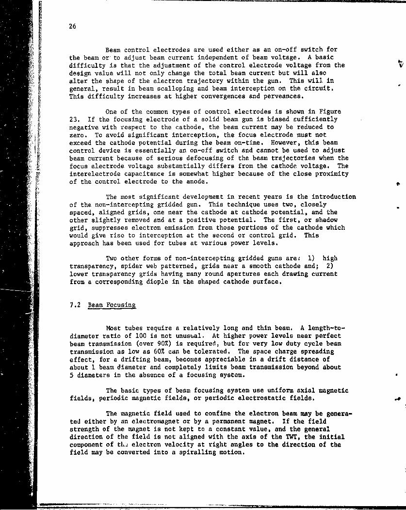
-F design value will not only change the total beam current but will alsoalter the shape of the electron trajectory within the gun. This will ingeneral, result in beam scalloping and beam interception on the circuit.This difficulty increases at higher convergences and perveances.
One of the common types of control electrodes is shown in Figure23. If the focusing electrode of a solid beam gun is biased Cufficientlynegative with respect to the cathode, the beam current may be reduced tozero. To avoid significant interception, the focus electrode must notexceed the cathode potential during the beam on-time. However, this beam
• Il ~control device is essentially an on-off switch and cannot be used to adjustbeam current because of serious defocusing of the beam trajectories when thefocus electrode voltage substantially differs from the cathode voltage. Theinterelectrode capacitance is somewhat higher because of the close proximityof the control electrode to the anode.
The most significant development in recent years is the introductionof the non-intercepting gridded gun. This technique uses two, closelyspaced, aligned grids, one near the cathode at cathode potential, and theother slightly removed and at a positive potential. The first, or shadowgrid, suppresses electron emission from those portions of the cathode whichwould give rise to interception at the second or control grid. Thisapproach has been used for tubes at various power levels.
Two other forms of non-intercepting gridded guns are4 1) high
transparency, spider web patterned, grids near a smooth cathode and; 2)lower transparency grids having many round apertures each drawing currentfrom a corresponding diople in the shaped cathode surface.
7.2 Beam Focusing
Most tubes require a relatively long and thin beam. A length-to-diameter ratio of 100 is not unusual. At higher power levels near perfectbeam transmission (over 90%) is required, but for very low duty cycle beamtransmission as low as 60% can be tolerated. The space charge spreadingeffect, for a drifting beam, becomes appreciable in a drift distance ofabout 1 beam diameter and completely limits beam transmission beyond about5 diameters in the absence of a focusing system.
The basic types of beam focusing system use uniform axial magneticfields, periodic magnetic fields, or periodic electrostatic fields.
The magnetic field used to confine the electron beam may be genera-ted either by an electromagnet or by a permanent magnet. If the fieldstrength of the magnet is not kept to a constant value, and the generaldirection of the field is not aligned with the axis of the TWT, the initialcomponent of th, electron velocity at right angles to the direction of thefield may be converted into a spiralling motion.
27
7.2.1 Uniform Magnetic Field
Ordinarily, the focusing magnetic field is derived from a longsolenoid which has iron shielding around the outside diameter and polepieces with small apertures for the beam at both sides. The magneticfield strength used is generally between 200 to 3000 gauss, but some-times as high as pole pieces magnetic materials will permit, such as,in the neighbourhood of 10,000 gauss for high frequency tubes. Wirewound solenoids are least expensive. Size, weight, and power requirementscan be reduced by increasing the packing factor of the conductors. Incases where weight and power savings are of extreme importance, such asin airborne applications, foil solenoids wound directly on the tubes havebeen used successfully.
One of the difficult tasks is to produce a distortion free (uniform)magnetic field. Two common problems are shuwn in Figure 24.
Unless the pole piece area is large compared with the spacing therewill be considerable bowing of the field lines. Unfortunately, large areapole pieces lead to high fluxes and very massive magnets.
Pole pieces may be made in appropriate shapes in order to minimize
bowing, as shown in the C-magnet, Figure 25.
pole A better arrangement is to employ a combination of solenoid andpole pieces Figure 26. The pole pieces act like magnetic mirrors, effectivelyextending the solenoid to infinity. However, even the highest-purity softiron is not a very good "reflector" and it is usually necessary to boost thecurrent at the ends of the solenoid to avoid field distortion.
Cooling must be provided for most electromagnets. For fields up to400 to 500 gauss forced air cooling is generally sufficient, but for higherfields, liquid cooling is usually necessary. Some foil-wound magnets,
, however, have been made to work with air cooling in the 1000 to 2000 gaussregion.
Many tubes requiring only a short interaction region may be focusedwith a permanent magnet. The end pole pieces of such tubes are joined byexternal permanent magnets. A cylindrical "pot" permanent magnet closed ateach end by soft iron plates may be used in some cases, as shown in Figure27.
For higher fields a barrel-shaped magnet with re-entrant pole"pieces can be designed. However, as the length of the magnetic material isincreased, the leakage flux rises and the cross-section has to be increased.However, the weight of the magnet will soon topple the advantage in fieldstrength obtained..
,Although the magnet power and cooling requirements have been
eliminated by using permanent magnets they are heavier than comparablesolenoids by at least a factor of 2. However, the advent of samariumcobalt will now permit a substantial reduction in the weight of thepermanent magnet.
28
7.2.2 Periodic Permanent Magnet (PPM) Focusing
PPM focusing is achieved by a series of magnetic lenses. The beamis focused within each lens and spreads from space charge repulsion betweenthe lenses. As the spacing of the lenses is increased from zero, thenecessary lens strength first rises and then falls. However, the fartherapart the lenses, the greater the variation in beam diameter.
The periodic magnetic field is usually obtained by stacking polepieces alternately with axially magnetized ring magnets as shown in Figure 28.The ring magnets are generally made of high coercive force magnetic material.An alternative configuration is the radial PPM structure, which employsradially magnetized sectors of rings at the outer diameter of the pole piecesand an iron outer sleeve to provide a magnetic flux return path. This designrequires magnets with a high flux-carrying capacity, and since the focallength of the lenses depends only on the magnitude of the field and not itsdirection field reversals are immaterial. On the other hand, reversing thefield greatly reduces the leakage field. Thus the magnets may be made muchsmaller in cross-section with a considerable saving of weight (sometimes morethan 10 times). It is this feature that gives PPM the advantage over non-PPMfocusing.
Converging magnetic lens focusing, Figure 29, was initially usedin helix TWTs and subsequently has found application in high power coupledcavity TWTs.
Recent improvements in magnetic materials have increased the easeof providing PPM focusing. The older Alnico (aluminium-nickel-cobalt alloy)and barium ferrite magnets have been superseded by Alnico 8 and Alnico 9 whichhave higher flux carrying capabilities, lower temperature coefficient, andhigher coercive forces. (Samarium cobalt has four times the magnetomotiveforce of Alinco 9, per unix length of magnetization.)
One drawback of PPM focusing is that the beam is not well focusedfor voltages below operating value. This may create tube body dissipationproblems in cathode-pulaed tubes during pulse rise and fall times.
7.2.3 Periodic Electrostatic Focusing (PEF)
Periodic focusing may also be produced by a series of electric lenses.I ~ A system of alternating positive and negative lenses of equal strength can
be used to focus the electron beam.
j •Some of the reasons why PEF has failed to find universal acceptanceare difficulty of analysis, fundamental limitations of capability to focus,and the relative complexity of tube construction. Unlike PPM focusing, thebeam is focused equally well at all beam voltages because electrostatic
* trajectories depend only upon the geometry of electrodes as long as all* j voltages are held in proportion.

29
SAn important limitation to achieve high power and high frequencyoperation is voltage breakdown between lens electrodes and the tube body.
7.3 Collectors
The collector is an electrode used to absorb the spent beam and theresidual energy of electrons. In low-power tubes the design of the collectorrarely presents any problem, but in high-power tubes it is essential to ensurethat the power dissipated over any area on the collector surface does not"exceed the safe limit for the material and the cooling system.
It is usual to remove the beam-confining magnetic field by passingthe electrons into the collector through a hole in a soft-iron pole piece.The beam after entering the collector entrance spreads, in the absence of amagnetic field, under the influence of its own space charge effect.
In beams having smooth flow at fields above Brillouiu the electronsacquire angular velocity upon leaving the confining field and suvsequentbeam spread will be faster. For this reason cylindrical pot collectors,shown in Figure 30, are designed to collect some of the beam current on theside walls.
The size of the collector is determined by both average and peakpower. Average dissipation density is normally limited to about i KW/Cm2 .Since beam interception in the collector is quite non-uniform, the surfacearea must be several times larger than that determined by average collectorpower. For pulsed tubes, the temperature rise during the pulse may becomea limiting factor. Two problems must be guarded against,-namely, surfacemelting during the pulse and cyclic stress in the material caused byexpansion and contraction during pulsing. These phenomena are particularlyimportant for tubes in the megrwatt range.
7.3.1 Depressed Potential Collectors
In order to increase overall tube efficiency, it is frequentlyadvantageous to collect the spent beam at a voltage below the interactionstructure voltage. Since electrons of various energy classes are present,this is done most efficiently by segmenting the collector and biasing eachportion at a different voltage. The amount of permissible voltage depressionis • termined by the velocity distribution in the spent beam, which differsfrom one device to another. The depressed collectors, Figure 30, aremosely used on TWTs which have a lower interaction efficiency (from 20 to30 percent). Typically, using a single-stage collector, 40 percent depressioncan be achieved in a high average power device, and 50 percent depressionat the lover power levels. Collector insulation, therefore, must besubstantial, The amount of depression is ultimately linked by thereturned electrons from the collector, which cause heating of the inter-action structure aod provides RF feedback.
4__••

30
These returning electrons (secondary current) may be suppressed byfitting a plate, with an aperture just large enough to pass the beam, acrossthe mouth of the collector as shown in Figure 31. A tilted plate is usedto collect the electrons that are turned back.
Finally it should be noted that the collector depression onlyallows the D.C. power input to a tube to be reduced. It does not allowthe RF output to be increased since to do this it would be necessary toincrease the beam power, and presumably this is limited by other considera-tions.
7.3.2 Methods of Cooling
For typical linear-beam tubes, from 50-80 percent of the D.C. inputpower is converted to heat. Substantial cooling of components must, there-fore, be provided if the average power is high. Although most of thecooling is required in the collector, some cooling is also necessary forthe interaction structure because of its heating by intercepted beam currentand RF losses.
Cooling is accomplished by convection, conduction, forced air,vapor phase and heat pipe, and forced-flow liquid, in the order of increasingdissipation density requirements.
Convection and conduction cooling are limited to devices of a fewhundred watts RF power output. Forced air, however, is used extensively upto several kilowatts level. Air cooled collectors are usually larger thanwater-cooled collectors because of the lover tolerable power density andlarger fans.
Forced-flow liquid cooling is by far the most commonly used systemfor high power linear-beam tubes. Although water is preferred as thecooling medium various concentrations of ethylene glycol solutions areused for low-temperature environments, and hydraulic fluids such as siliconeoils are used for airborne applications.
Vapour phase cooling takes advantage of the latent heat of waterevaporation by allowing it to boil at the collector surface. The steam isthen condensed in a heat exchanper and returned to the collector, forminga closed system. Vapour phase cooled collectors have found application Intubes up to the 50 KW output level.
"8.0 "AT.ENATICAL FORMUTION OF TWT
In order t~o obtain some theoretical understanding about thebehaviour of the TWT a number of assumptions are necessary to simplifythe analysis. Using small signal analysis the equations governing the

31
A 1 electron flow can be linearized by deleting certain quantities which arenegligible and a wave type solution can be achieved.
Some of the main simplifying assumptions used to arrive at asolution are:
a) Electrons in the electron flow are acted onby the same AC field when the diameter ofthe electron beam is small (constant axialfield).
b) Electrons are displaced in the axialdirection only, (no transverse motionof electrons).
c) The attenuation in the slow-wave structureand the effect of space charge are neglected,(lossless circuit).
If one considers that the signal current in the circuit is theresult of the distributed electron stream acting on the circuit and thedisturbances on the electron stream is the result of the fields of thecircuit acting on the electrons, the problem can then be divided intotwo parts.
i) The Circuit Problem - to Utn0 the field acting onthe beam in tercs of thedriving current supplied by
icrthe beam,
ii) _The_ Eletronic Prob.lem to find the current in thebeam in terts of. the fieldacting on the beam.
Overall behaviour of a IVT ay be obtained by combining thesolutions of these two parts.
The mathematical model for the small signal operation of a 1Wcan be developed from the work of Grittina and Pierce. In a travelling-wave tube both the voltage and the current converge to the eaae rate ofexponential grooth and reach a constant phase dlfferenceý This suggeststhat the travelling-vave amiplification can be expresed in teomt of awave equation of the form.
aep (wt - r z)
*here r is the coaplex propagation ,nstant,
The equivalent circuit used by J.R. Pierce has distributed series inductaaceL and shunt capacitance C with current I and voltage V, as shoun in Figure

32
32(a). Because the charge density in the electron beam at any point variesperiodically with time it induces a current J, in the capacitors given by,
J - O dZ (5)
where p is the AC component of the charge per unit length.
However, conservation of charge states that,
= -6z (6)
From (5) and (6)
j = -- dZ (7)
From Figure 32(b) and (c) we get
dv= _- JiLI (8)
z= -(jWCV + ) (9)
Since all quantities vary as exp (jwt - rz) equations (8) and (9)wnay be written as
rv = JWLiand FI = jwCV - rI
Eliminating I, we get
v - jrWLi (10)r! 2 +-wLC

33
Assuming that the electrons pass very close to the slow-wavestructure, the field E acting on the electrons is given by
EAV jriLi (11)77 S = 6Z r 2+Wi 2LC
The total convection current must be equal to the total chargedensity times the total velocity.
(I +i) =Po (P + p) + V(P + p) (12)0 0 0 0
* where p is the average beam velocity
p is the average charge per unit length
v is the AC component of the electronvelocity
p is the AC component of charge perunit length
1 is the DC beam current (negativeper electrons beam)
"Neglecting the product terms of AC quantities equation (12) reducesto
. p + VP° (13)
Since we are interested in small signal analysis we only want todeal with linear differential equations. Therefore, we can replace thedifferentiation with respect to time by multiplication by jw and differentia-tion with respect to distance by multiplication by -. Thus, the conservationequation (6) becomes.
jwp Iri
or P = (14)

34
Substituting equation (14) in equation (13)
i = p+j (15)
Electron velocity v is a function of electron mass m, and theelectron charge e.
The time rate of change of velocity is equal to the charge-to-massratio times the electron gradient.
d (p +v)0 e 6
dt xT
Under small signal conditions, the AC velocity v can be shown,
e
- a V (16)JW-Fjo
Substituting equation (16) in equation (15) we get
ji orv0
(7- 2Vo( -r)2 (17)
where 8p-• I V and o = 2 -V0 00 0 00
where V is the D.C. beam voltage.0
Equations (10) and (17) involve both V and i and, therefore,combining them we get the overall equation.
-- i:••(2°°(B r)2 ('2r,) 1 (18)8 0

35
where Z is the characteristic impedance
Sand r1 jw vTc, the natural propagation constant.
Equation (18) applies for any electron velocity, specified by • and any wavevelocity and attentuation, specified by the real and imaginary parts of the
F propagation constant r.
Equation (18) contains the fourth power of the propagation constant r and,
therefore, this suggests that the travelling-wave amplification may beexpressed by four waves.
A complete analysis of this fourth power equation will reveal:
t a) one wave which is increasing, travelling slowerthan the beam;
b) second one which is decreasing, travelling slowerthan the beam;
c) third one which is unattenuated, travelling fasterthan the beam;
d) the fourth one which is an unatcenuated wave,travelling backwards,
In the forward direction, there is a cumulative interaction betweenwaves and electrons because both are moving at about same speed and theincreasing wave becomes dominant. The wave travelling against the electronflow is less affected because the wave and electrons are moving in oppositedirections.
Two physically significant parameters are the power flow in thecircuit and the electron field associated with it which acts on the electronstream. In terms of the magnitude of the voltage the magnitude of field isgiven by, E = rV.
The power flow in the circuit is given, in terms of circuitvoltage, by
• .• P= 2T(19)
I' ~ 2Z0
S°I

36
Therefore, Z =E(2o 2r2P (20)
8.1 Travelling-wave Tube Gain
The most valid relationship between gain and power output is givenby Pierce. It can be seen that the process of calculation of gain is rathercomplex and involves large number of parameters.
For the case of a no-loss circuit and an electron velocity equal tocircuit phase velocity, the three forward waves are set up with equalvoltages, each given 1/3 of the applied voltage.
That is V V1 V V (21)1 2 3 (21)
Vand V V V (22)
1 2 3 3
where V is the total beam voltage at distance Z 0. If V is the voltageat distance Z, the gain can be expressed as
Vz
G 20 log V (23)V
Expanding this concept, Pl.erce suggested the fundamental equation for gain
G (A + BCN) dB (24)
where A is the loss in initiating the amplified wave (approx.10 db)
B is the factor depending mainly on the exactrelation of the beaw to the circuit velocities
C is the gain parameter
N is the number of active wavelengths in thetube.
The quantity C is related to the characteristic impedance, Zo andthe beam impedance by,
S',i:" !"!".'•'.,. •,.•: •. .,•i..:•_, •...... .......... .....-.-......-. -.. : • ••... ... .

37
C3 = o (25)o4V
0
Therefore, CS is the circuit impedance times • the beam impedance.
8.2 The Effect of Space Charge
In deriving the above equations one of the assumptions made wasthat the effect of space charge in the system was negligible. However, inpractice there is an additional force on the electrons due to their mutualrepulsion, and this can be accounted for in terms of a space charge field.Pierce suggested that the effect of space charge could be represented by acoupling capacitor between the beam and the circuit as shown in Figure 33.
The space charge field is IL where C, is a new parameter which has the
dimensions of capacity per unit length. If the current through this capacitoris - or ri; then the voltage dropped across the capacitor is 4U
The equivalent voltage acting on the beam, V = V - (26)
where V is the circuit voltage.
A.•!• ~ ~The total field acting on thte electron, E = "'
IN - (27)
Now equation (10) can be rewritten in terms of rl, and Zo, as
V 0- o (28)
Similarily equation 01) becomes
.. ,-Ar~r zS= - 0.- (29)
(r2-r =
. . . ..

38
Thus equivalent voltage, equation (26), and total field, equation (27),becomes.
rr zv1 0 [ 1 (3011
and
r2r zl (r2_-) (31)
Equation (18), the overall equation, may be modified as
SI F rFr zo o(32)
2V (j-W-)2 (F, 2-F 2 ) WC,0
Equation (30) may be simply written as
V1 =V-Vs
where V is the voltage due to the space charge. The terms in the bracketef equation (30) represent impedance. If tei wuavelengtn of the impressedcurrent is long or if the wave is faster than the natural phase velocityof the circuit, the inductance has a higher impedance 'than the shuntcapacitance to ground; the capacitire effect predominates and the circuitimpedance is capacitive.
8.3 The Helix as a Spiral Slot Transmission Line
As discussed earlier, the helL: can he regarded as a spiral slot
transmission line, around whb.ch the energy propagates at-approximately thevelocity of light. The lont-itudinal travelling field ou the axis is ofthe form,

"39
LZ
Esin W (t--) (33)
P
The phase velocity of the axial field is given by v c sin X*' where c is
the velocity of light and X is the helix pitch angle.
The radial propagation constant y is defined by
Y 2 a2 a3o2 (34)~A 1 0
where 8 = and 8 = from which,p
v 0 (35)
c
B is the phase constant of the wave travelling with the speed of
light, which would vary with distance in the z direction as exp (-Ji z).0
The actual phase constant, 8, varies with distance as exp (-JBz).
8.4 Phase Velocity and Group Velocity
The velocity of the axial field of a helix of pitch angle X isgi-ven by
v c sinx (36)p
On a w-B diagram (frequency-phase diagram) the phase velocity at any pointis the slope of the line joining that point to the origin, as
*This approximation is valid over the range around four turns per wave-length where helices are normally operated. It ceases to be valid whenthere are large number of tnrur per wavelength.
77~

40
¼pv (37)p
The electron beam can be represented by a straight line through the origin,whose slope is the beam velocity. Where this line cuts the frequency-phasecharacteristic, the beam and natural circuit wave velocities are equal andconditions are right for synchronous operation.
The slope of the frequency-phase characteristic is given as thegroup velocity, Vg
V =w (38)
Group velocity is the velocity at which the energy travels in the slow-wavestructure. It is the velocity with which the group of frequency components,making up the pulse, travel down the circuit. It is the propagation velocityof the energy stored in the electric and magnetic fields of the circuit.
Figure 34 shows a radio frequency pulse varying with time as f(t).The envelope varies with time as F(t), The pulse may be produced bymodulating a radio frequency source with F(t).
Mathematical analysis show, if a pulse envelope, as shown inFigure 34, is applied at the input, the output will be of the same shapeas the input, but arrives a time T later, where
go (39)dw
when k is the length
This implies that it travels with a velocity V , where,
V LW (40)vg dO
Since V = , the group velocity V may be derived as follows.
Rearranging-the equation for phase velocity, we get
W(41)Vp
..- |-

Differentiating
dV .a
p V
1 dV(42).i -*# E.)Vp VpiI
from (40),
- dV
V•(4P 3)
dV
p
For interaction of electrons with a wave to give gain in a TWT, the electronsmust have a velocity near the phase velocity V. Haence, for gain over a
pbroadband of frequencies, V must not change with frequency and if V does
dV p
not change with frequency then - 0 and V V$ P
8.5 Coupled-Cavity Structures - A Lumped Circuit Model
The general behaviour of €ouplad.cavity structures may be studiedby analysing its lumped circuit analogy. This approach is much easier than
"Ilk using FAxwellts equation which becoses very'difficult due to the complicatedboundary conditions imposed by the geomtry of the structures.
The Chodorow-Nalos stmcture, discussed earlier, may be representedby its lumped circuit shown in Figure 35. Bach cavity can be repreoented bya resonant circuit made up of a condencer C19, :an. -nIductance 4L1, thatthe resonant irequenty- w Is given by:
- -. t.' . .,

42
The coupling slots between adjacent cavities are represented by a parallelcircuit made up of C2 and L2 . Thus the slot resonant frequency a3
1
The circulating current in each cavity can be divided into threeparts, one which links the coupling slot to the previous cavity, anotherwhich links the coupling slot to the following cavity and the third onewith no linkage. This has been represented by splitting L, into the
2L 2I L where k is the fractionparallel structures of magnitude k w k i tefci
of the coupling current whic'ý. takes part in the coupling. These are shownin the lumped circuit model, Figure 35(a). This circuit may be reduced tothe basic cells shown in Figure 35(b).
The values of ZA, ZB and Z are shown below, where,•A BA - _
2jWLA k
-' i 2jwL
B 1 -k - 2 LICI
JwLand Z 2
1 - 2L2 C2
It ie suggested that the reader consult Gittine for a thoro '1discussion of this subject.
8.6 Hollow Beams
The physical size of the TWT tends to be inversely proportionalto the centre frequency. The use of hollow electron beams provides much'higher values of total perveance thereby offsetting the requiro-ment for alarger tube size. Typical hollow beams used in VHF tubes have perveances
Sof the order of 100 x 10-6 as compared with typical high frequency solid"beam tube perveance of the order of 1 x 10- The results of operation atthese high values of perveance is the possibility of using much lower beamvoltage for a given beam power that can be used An low perveance tubes.The gain of the TWT in dB is proportional to the number of wavelengths iuthe tube at the electron velocity and to gain per:Wavelength.Phoe gPtn
- ,

43
per wavelength is increased by increasing the beam perveance and the'wave-4length is decreased an the voltage is decreased, so both factors favour a
shorter tube when perveances are increased.
The bandwidth and the gain may be increased, as the frequency isincreased, if the thickness of the beam is increased. However, as the
- current in a thick hol3ow beam -a increased, the potential of the innnerelectrons is depressed in comparison with the potential of the outerelectrons, as r result of an increasing space charge in the beam.
* Under certain conditions hollow beamý- become unstable in that thebeam breaks up into separate beams. In the presence of the magnetic fieldthe excess charge preduces a displacement of the nearby electrons. As thebeam current is increased from a very low value the initially circulartrace departs from circular symmetry, both in shape and brightness.Further increase causes the beam L-. curve away in a number of places,eventually forming a separate beam. The number of beams depends on thecurrent density and the magnetic field.
Electrost.ýtic focusing methods may be used in order to completelyeliminate the magnetic field in the circuit region of the tube. This methodis uniform in contrast to the various periodic focusing systems and is
d I advantageoua Lor certain applications. See Figure 36 for gun designs,
The interactton impedance of a lossless helix is given by
. E2Z - --
0 2BP
wherq E is the electric field in the direction of beam velocity,
0 =V V being axial phase velocity of the waveV Pp
J0 a, c being the velocity of light
P = power transmitted for a field EY = o2 s-
For a hollow beam at a radius r (Figure 37), the Impedaace at r isegiven by o
p ill. : N. . *
-. . . .:•, , *,~ , , .*,,, '

44
30 3 -2y(a-rO)J 00% Iwhere 'a' is the radius of the helix.
For voltages, below 10 Yv, 0>0> and Y and 8 may be used interchangeably.A 0
30 e -2y(a-r )Thus Z 3 e o S• o
600
(,c_() 30 e 2yar-p Yro
9.0 CONCLUDING REMARKS
The TWT is a 'mnture device' and no major break-through in itstechnology is anticipated, However.: the•re is ample room for improvenUnt -practically in every aspect of TWT parameters.
-Because of the high power, and increased bandwidth requirements,- radar and electronic countermeasures are turning their attention moea and
-4.. wore to sWT,.. We1T have also penetrated deep into, Co~umications Satellite.4 Technology.
The use of the computer in simutlating and analysiog TW1 parameterswill be a key factor for futture improv•ments. A good exawple of this is thedevelopmeat of a large signal computer prograto to study the beam-circuitinteraction in the 200w TWT used for the Comuications Technology Satellite.
'•- As power level increase and high freque•cy bands bscome moreattractive1 , 114T& will rezain unchallenged in years to come.
• .: .... . . . . . .

45
REFERENCES
1. A. Staprans, E.W. M~cCune and J.A. vuetz "High Power Linear Beams Tubes".Proceedings of the 1 EEE, Vol. 61, No. 3, March 1973.
2. J.T. Mendel "Helix and Coupled-cavity Traveling-Wave Tubes". P oceedingsof the 1EEE; Vol. 61, No. 3, March 1973.
3. F.N.H. Robinson and R. Kompfner, "Noise in Traveling-Wave Tubes".Proceedings of the IRE, August, 1951.
S4. D.G. Dow, "Behavior of Traveling-Wave rubes Near Circuit Cut Off".IRE Transaction on Electron Devices, July 1960.
5. M. Chodorow and R.A. Craig, "Some New Circuits for High-Power Traveling-Wave Tubes". Proceedings of IRE, August 1957.
6. D.A. Dunn, "Traveling-Wave Amplifiers and Backward-wave Oscillators forVHF". IRE Transactions on Electron Devices, July 1957.
7. J.R. Pierce, "Instability of Hollow Beams". IRE Transactions on ElectronDevices. October 1956.
8. CB. Crumby, "A VHF Traveling-Wave Amplifier Tube Employing an Electro-static•lly Hollow Beam". IRE Transactions - Electron Devices, January1956.
9. H. Sobol and J.E. Rowe, "Theoritical Power Output and Bandwidth ofTraveling-Wave Amplifier's". IRE Transactions .on Electron Devices,April. 1960.
10. D.J. Conaolly and T.A. O'Malley, "A Contribution to Computer Analysisof Coupled-Cavity Traveling-Wave Tubes". 1EEE Transactions on ElectronDevices# Vol., ED. 24, No. I Jan. 1977.
i )). fA, Vatkins and D.G. Dow, "Strapped Dif iar for High-Peak-PowerTraveliug-Wave Tubes". IRE Transactions on Electron Devices,January 1959.
12. D.C. Buck, "Traveling-Wave Tube Interaction Circuit". Correspondence,IEEE Transactions on Electron Devices, October 1967.
13. S.E. Webber, "Calculation tf Wove Propagation on a Helix in theAttentuatiou Region". Presented at 1953 West Coast IPw-AIEE
*•-- Confereace on Electron Tube Research.
14. W.A. Watson and J.R. Miannery, "Study of a Plane Short on a Shielded2 Helix". IRE Transaction - Electron Devices, October 1955.
i, a

4-ý
15. R.W. Gould, "A Coupled Mode Description of the Backward-WaveOscillator and the Kompfner Dip Condition". IRE Transactions- Electron Devices, October 1955.
16. C.K. Birdsall and T.E. Everhart, "Modified Contra-Wound Helix Circuitsfor High Power Traveling-Wave Tubes". IRE Tranfaction on ElectronDevices, October 1956.
17. J.A. Lucken, "Some Aspects of Circuit Power Dissipation in High PowerC.W. Helix Traveling-Wave Tubes". Part I: General Theory, Part II:Scaling Laws, IEEE Transactions on Electron Devices, Vol. ED. 16,No. 9, September 1969.
18. W.G. Worcester, A.L. Weitzmann and R.J. Townley, "Light-weight AluminumFoil Solenoids for Traveling-Wave Tubes". IRE Transactions ElectronDevices, January 1956.
19. H.R. Johnson, T.E. Everhart and A.E. Siegman, "Wave Propagation onMultifilar Helices". IRE Transactions on Multifilar Helices". IRETransactions - Electron Devices, January 1950.
20. H.G. Kosmahl and P. Ramins, "Small-Size 81- to 83.5 Percent Efficient2- and 4 Stage Depressed Collectors for Octave-Bandwidth High-PerformanceTWT's". IEEE Transaction on Electron Devices. Vol. ED. 24, No. 1,January 1977.
21. M.J. Schindler, "An Improved Procedure for the Design of Periodic-Permanent-Magnet Assemblies for Traveling-Wave T'ibes". IEEE Transactionson Electron Devices, Vol. ED. 13, No. 12, December 1966.
22. M.S. Glass, "Straight-Field Permanent Magnets of Kinimui Weight forTWT Focusing-Design and Graphic Aids in Design". Proceedinga of theIRE, August 1957.
23. J.T. Mendel, "Magnetic Focusing of Electron Beams". Proceedings of the
IRE, March 1955,
d 24. C.C. Cutler and M.E. Hines, "Thermal Velocity Effects in Electron Gu&s".Proceedings of the IRE, March 1955.
25. A. Nordsieck, "Theory of the Large Signal Behavior of Traveling-WaveAmplifiers". Proceedings of the IRE, May 1953.
26. T. Kageyama, Y, Morizumi and E. Watanabe, "A Large-Sipjal Analysis ofBroad-Band Klyskrons with Design Applications". IEEE Tranksactioua 'Da
Electron Devices, Vol. ED. 24, No. 1, January 1977.
27. A. Kiel and P. Parzeu, "Non-linear Wave Propagation in Travoling-Wave• • •i•.Amplifiers". IYE Transactions - Electron Devices, October 1955.
28. S. Sensiper, "Electromagnetic Wave Propagation on Helical Structures".Proceedings of the IRE, February 1955,
• .-,

47
29. I.P. Kaminow, R. Kompfner and W.H. Louisell, "Improvements in LightModulators of the Traveling-Wave Type". IRE Transactions on MicrowaveTheory and Techniques, September 1962.
30. J.R. Pierce, "An Interesting Wave Amplifier". IRE Transactions onElectron Devices, April 1960.
31. A.R. Iverson, "High Average Power Dissipation in Helix Tubes". IRETransactions on Electron Devices, April 1960.
32. K. Miyauchi, "Traveling-Wave Tube Nanosecond Pulse Generator in 24- Gc Region". IEEE Transaction on Microwave Theory and Techniques,January 1963.
33. C. Loo, "Calculation of the Suppression of Signals and IntermodulationNoise when Multiple Unequal Carriers are Amplified by a TWT". Presentedat the Canadian Communications and Power Conference, Montreal 1976.
34. C. Loo, "Calculations of Intermodulation Noise Due to Hard and SoftLimiting of Multiple Carriers". Presented at the ICC, 1974.
35. L.M. Field, "Some Slow-Wave Structures for Traveling-Wave Tubes".Proceedings if the IRE, January 1949.
:36. M. Scotto and P. Par.:en, "The Electronic Theory of Tape-Helix Traveling-Wave Structures". IiE Transactions - Electron Devices. October 1955.
37. iE.R. Warneke, W. Kleen, A-. Lerbs, 0 Dohler and H. Huber, "The Magnetron-.Type Traveling-Wave Amplifier Tube". Proceedings of the IRE, May 1950.
386e W.H. tLouisell, "Approximate Analytic Expressions for TWT Propagaý.ion. "",Constat" IRE Transactions on Electron Devices, October 1958.
::.39. E.J- Nalos, "A Hybrid Type Traveling-Wave Tube fc.r high-Power Pulsed9... Amplificatlon". %IRE Trxnsaction9 oen Electron Devices, July 195.5.
40. 14. Meyer, T. Vati Duzer, "Trwing-ve Amplif.4•ati~n and Power Flowin.io.1uct.tn gallds". IEEE Transactions on EIL-ctron Degicas,.- March
-- '. .(, - .
" 41. R.W. GerchtIrg, K.B,.Niclas, "The Positively Taperad Trzveling-.Wave!t%. ube&. Correspondence,, IEEE trausaction. on Electron DWvicesi--September 1969.
42. X., lRoney and E.M.T.. Jonoes, "A Wide-Band UIF Traveling-tlava Variable,-,actance Amplifier IRE Transaction or Ricrowave Theory and. Tochniqueu,May 1960,
aae,''eeti So-ai4:! 43. R.H. r aetll, F.D. Coleu\n and 11.C. becker, "Dieectri Slow-Wave.•Structures for ttIa Ganoration of Power at Millimeter and Sub
S• "illi~eter Wavelengths", IRE Tranrsactions on Electooo Devices,July 1958.
4,

48
44. O.L. Hoch and D.A. Watkins, "A Gun and Focusing System for Crossed-field Traveling-Wave Tubes". IRE Transactions on Electron Devices,January 1959.
45. C.C. Cutler and D.J. Brangaccio, "Factors Affecting Traveling-WaveTube Power Capacity". IRE, Vol. ED. 3, June 1953.
46. D.A. Dunn, G.S. Kino and G.W.C.M.C. Mathers, "Traveling-Wave TubePropagation Constants for Finite Valuee of Gain per Wavelength",
IRE Transaction on Electron Devices, October 1958.
47. J.J. Caldwell Jr. and O.L. Hoch, "Large Signal Behavior of HighSPower Traveling-Wave Amplifiers". IRE Transactions - Electron
Devices, January 1956.
4.8. J.E. Rowe, "A Large Signal Analysis of the Travelling-WaveAmplifier: Theory and General Results". IRE Transaction- Electron Devices, January 1956.
49. P.K. Tien, L.K. Walker and V.M. Wolontis, "A Large Signal Theory ofTraveling-Wave Amplifiers". Proceedings of the IRE, March 1955.
50. L.J. Chu and J.D. Jackson, "Field Theory of Traveling-Wave Tubes".Proceedings of the IRE, July 1948.
51. J.R. Pierce and L.M. Field, "Traveling-Wave Tubes". Proceedings ofS..the IRE, February 1947.
•!iSj>i52. J.R. Pierce, "Theory of the Beam-Type Traveling-Wave Tube". Proceedingsof the IRE, February 1947.
!$ 53. PK. T -, "Traveling-Wave Tube Helix Impedance". Proceedings of theIRL, November 1953.
54. S. Millman, "A Spatial Harmonic Traveling-Wave Amplifier for SixMillimeters Wavelength". Proceedings of the IRE, September 1951.
55. J.A. Boyd, D.B. Harris, D.D. King and H.W. Welch, Jr., "ElectronicCounter Measures". Prepared by the Institute of Science and"Technology of the University of Michigan for the U.S. Army SignalCorps. Published in 1961.
56. H. Chodoeow, E.K. Ginzton and E.J. Nelos, "Debunching of Electron BeamsConstrained by Strong MNaetic Field". Proceedines of the IRE, August1953.
57. D.A. Watkins, "Low Noise Traveling-Wave Tubes for X-Band". Proceedingsof the IRE, December 1953.
58. F.K. Mullen, "Traveling-Wave Tubes with Ferrite Attenuators". IRETransactions on Electron Devices, July 1961.
,t

49
59. M.R. Currie and D.C. Forster, "The Gain and Bandwidth Characteristics7 of Backward-Wave Amplifiers". IRE Transactions on Electron Devices,
January 1957.
60. N.H. Pond and R.J. Twiggs, "Improvements of Traveling-Wave TubeEfficiency Through Period Tapering". IEEE Transactions on ElectronDevices, Vol. ED. 13, No. 12, December 1966.
61. S.A. Cohen, "Traveling-Wave Tube Gain Fluctuations with Frequency".IRE Transactions on Electron Devices, January 1957.
62. L.W. Holmboe and M. Ettenberg, "Development of a Medium Power L-Band Traveling-Wave Amplifier". IRE Transactions on Electron Devices,January 1957.
63. C.K. Birdsall and C.C. Johnson, "Traveling-Wave Efficiency DegradationDue to Power Absorbed in an Attenuator". IRE Transaction on ElectronDevices, January 1959.
64. A.G. Mungall, "Noise in Traveling-Wave Tubes". IRE Transactions -
Electron Devices, April 1955.
65. J.W. Sedin, "A Large Signal Analysis of Beam Type Crossed FieldTraveling-Wave Tubes". IRE Transactions on Electron Devices, January1962.
66. A.H. Iverson, "Precision Helix Winding and a Mechanism of Loss Variation",p.p. 205-206, IRE Transactions on Electron Devices, October 1956.
67. C.C. Cutler, "The Calculation of Traveling-Wavb Tube Gain". Proceedingsof the IRE, August 1951.
68. R. Kompfner, "The Traveling-Wave Tube as Amplifier at Microwaves".Proceedings of the IRE, February 1947.
69. S.E. Webber, "Electron Bunching and Energy Exchange in a Traveling-[Wave Tube". IRE Transactions on Electron Devices, January 1957.
70. W.E. Mathews, "Traveling-Wave Amplification by Means of CoupledTransmission Lines". Proceedings of the IRE, September 1951.
71. H.R. Johnson and J.R. Whinnery, "Traveling-Wave Tube Oscillators".IRE Transaction on ED., August 1954.
S72. C.K. Birdsall and G.R. Brewer, "Traveling-Wave Tube Characteristicsfor Finite Values of C". IRE Transaction on Electron Devices,Vol. E•-l, August 1934,
73, J.J. Caldwell, Jr., "High Power Traveling Wave Tube Gain and SaturationCharacteristics as a Function of Attenuator Configuration andResistivity". Trans. IRE, PGED, Vol. 4 December 1953.
V.I

50
74. A.W. Scott, "Why a Circuit Sever Affects Traveling-Wave TubeEfficiency". IRE Transactions on Electron Devices, January 1962.
75. J.F. Gittins, "Travelling-Wave Tubes", New York American ElsevierPub. Co., 1965.
76. J.R. Pierce, "Travelling-Wave Tubes", New York Van Nostrand, 1950.
77. King, S.E.R.L. Tech. J., Vol. 4, p. 9, 1954
78. Mathias and King, IRE Transaction on Electron Devices, Vol. ED. 4,p.28, 1957.
Mim
- - .,
.I
N

51
"-7
21i
II
£i?" i• i FIGURE, - PORTION OF THE TRAVELING-WAVE AMPLiPIER PERTAININGTO FLECTRONIC INTERACTION WITH RADIO-FREQUENCyFIELDS AND RADIO-.pREQURjCy GAIN
-I"
T
SINPUT COLLECTON
A W 'IG•• 2 - SCI!EMA1IC OF T118 M4VEL2WG-WAVjM P.•
..47No

52
SLOW-WAVE STRUCTURE
INPUT SECTION OUTPUT SECTION
0 N COLL CTOR
vvOUTPUT
ELECTRON BEAM
INPUT OUTPUT
SEVER LOADS
FTGURE 3 - TWO-SECTION SEVERED TRAVELLING-WAVE TUBE
INPUT OUTPUT
DIRECTION OF(0, POWER FLOW
GUNCOLLECTOR
BEAM OUTPUT INPUT
GUN DIRECTION OF '
k'IGURE 4 - DIAGRAM SPOWING DiRECTIONS OF ELECTRON AFID POWER FLOW
FOR: (a) NOElMAL TRAVELLING4IAVE TUBE (FORWARD WAVE.AKfPLIF'IER) , (b) BA CJWARD WAVE; ANZLIF.W?
TORI ____________OF
L'C4O FO

53
POLE PIECES
0E
ELECTRODE U ALLY A 8V EAM F.~ISLOW-WV CTURE) LCTRODE ($OLEIý
FIGi'N 5 -CROSSED-FJLD TWT
SLOW-WAVE STRUCTURES
UNIFORM STRUCTURE PER~ODIC STRUCTUREHELIX COUPLED CAVTIES
FIGURF 6 - SLOW WAVE STRUCTURES
A.,
"77. 77-77
. -- - -. .- -•s. ."

54
* A
FIGURE 8 -SHF4H NELX
*1 ?IGURMM8TAP" EU

FIGURE 10(a) - BIFILAR WIRE HELIX
FIGURE 10 (b) - BIFILAR TAPE HELIX
FIGURE 10(o) - STR4PE DI4 MW HIELIX::
IGORE 10(d), RING AU!) M4?C~R AUUN c
FI. . E 10 - •itI S2WUC.U• .
"*"" " "" I
"~ 7 7. .."Z7.: .":. • .:....7.:i)i

56
FIGURE 1 (a) - INTERDIGITAL LINE FIGURE 11(b) SLOTTED RIDGE WAVEGUIDE
FIOIRE 11 (0) -, INTERNAL HELICAL- FIGURE. 12(d) -DI$S-ON-ROD CIRCUITWAVEOUIDE 2IRUC!URE"
/0S..... . . . - . .... "
"PrWUR 1240). A" WTURED-DISK FGuI 2.. (f) -AI WASh.-, ."•. E•,uS ,IC. - UW CX.RCUX•(f A• -AaIZ::.• •. -
P•WR 11 , LW AE •CU

I FIGURE 12 -COUPLED CAVITY J5TRUCTURE ,f2roDoR~OW-NALos -zrRrCo./URE)
FIGURE 2 3 M TE .'HU (11ES STRUCTURE
IXUE4 TS

58
FIGUR 25 (a) - ECTANgGULAR S.TRUC2uRE FIGURS 36(b) -PAI gLtAJoGRAJSI TRU4CTUR
F rGUE 26 c) lOURGLA5S" S-TRUCTURE, FIGVR9 1 d) - "CLOVER LA- .JVT
FIGURES IS COUPLED-CAVITY STRUC2JRW
tocus,.eq 14E ME$14 owWDL AOTUSUALLY
ýjPIGURS-16 -- P2ER4 Go &

. - -. n j, . -- --.-. "
59
EJL2r
FOCW$NO
fa W AN= AP~ERTfL5 GI LENSES OF cowA. STRENTh."" " ' " W N IsVJRSD IN A .*V PARALLEL
(c) t&GLkaE SAE CHARG ASSUVEM
Y TRANSI TIME CENW4M ANOS tS HALF A CflOTRC?.......... ," ., . '
Pl:. /Rb. 17 - TWO AW.b . S-OMENA.. C
!LOW
kE" Et.rCTRON4 DIS1'$WBUT4 At tAAniS PLAtES
t - ~CATNC
A ~ ~PTOt/US Id - GO/ PASIGWE 3Y M4TUAS ACC'ORD/PIG, W~ Nt/LISP' PRThvathL"", ". • T
* 'i'i*-,.. " i.. *., , -.

60
N INTENSEODFFUSE" ;L- LOW
I 3 5 7 9BEAM ELECTRON DISTRIBUTION AT VARIOUS PLANES
FOCUSING POLE PIECEELECTRODE , .. A~ANODE
CATHODE BEAM PROFILE
SI i I I•: 3550
1 3-ii
FGUURE 19 - MATHIAS AND KING'S HIGH-VOLTAGE VERSION OF MULLER-TYPE GUN
END VIEW SIDE VIEW
4 FIGURE 20 - PERSPECTIVE VIEW SHOWING PATHS OF OUTER EL.,rTRONS

* 61
ANODE
CATHODE
•i-- -_ -Z - - - - - _
GUN MAGNETIC FIELD)
•:IRO POLE PIECE
FOCUSING ELECTRODEFIGURE~ 21 -A PRACTlICAL ARRANGEMENT FOR LAUNCHING BRILLOUIN FLow
FOCUSING ELECTROOE IRON POLE PIECE
CATHODE
-------------- MAGNETICFIELD LINES
LARGE HOLE INANODE POLE PIECE
BUCKING COIL
UIG0 22 - A PPARCTICAr, ARRANGEME-NT FOR LAUNCHIVG SMOOTH FLOW ATFIELDS ABOVE BRILLOUIN
,' . .
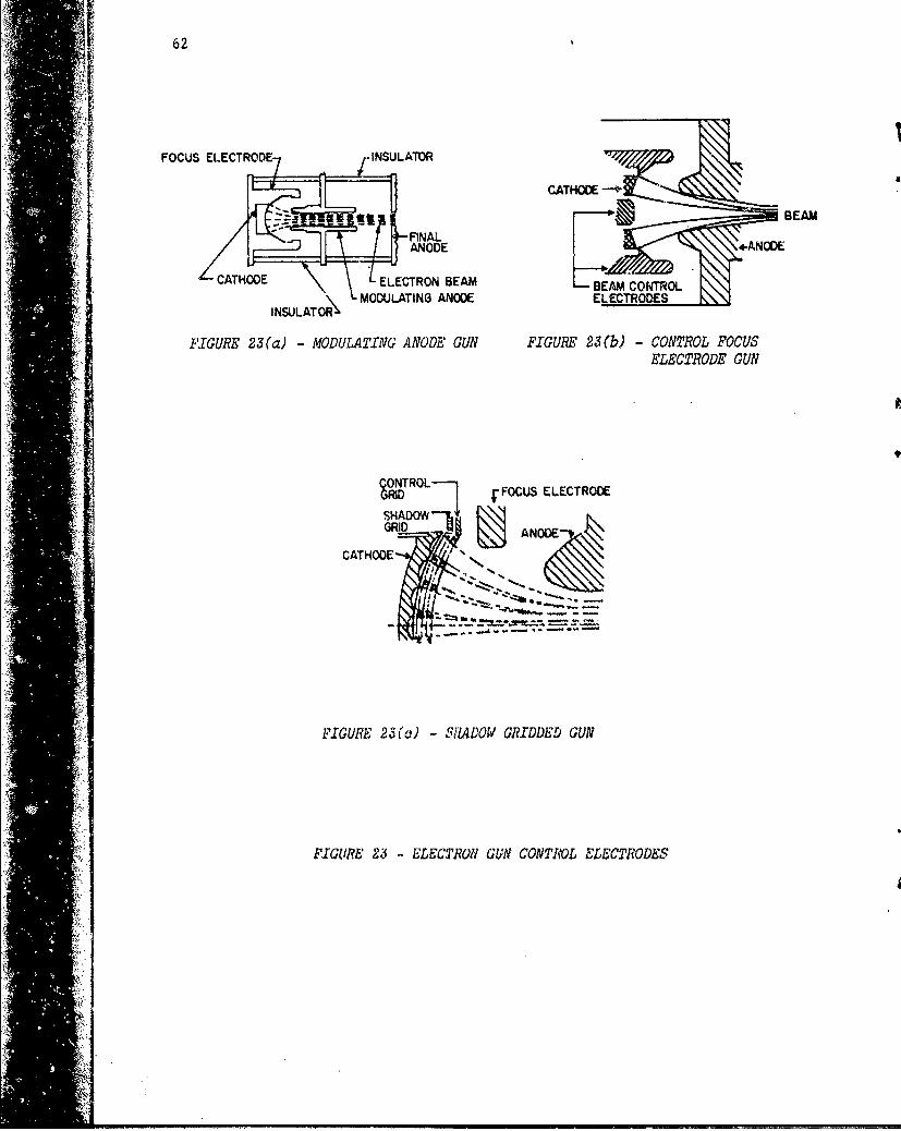
62
FOCUS ELECTRODE -NUAO
CATHODE-'
BEAM
ANODE ANODE
CATHODE ELECTRON BEAM BEAM CONTROLINSULATOR MODULATING ANODE ELECTRODES
FIGURE 23(a) - MODULATING ANODE GUN FIGURE 23(b) - CONTROL FOCUSELECTRODE GUN
FI'GURE S3c HADOW GRIDDED GUN
FIGURE 23 -ELECNTRON GN CONTROL ELE CTDODES

~ 63
I ~ kLdLLLLL•- SOLENOIDI •. Field distortion chacteristic of finite pole pieces.
Field diskfviior, choracterislic of finite solenoids.
FIGURE 24 - BOWING OF FIELD LINESPOLE PIECE
IRON CORE COILFIGUIJC 25 - C-.MAGNET
BARS GIVING RETURNPATH FOR FLUX
SOLENOIDEND PLATES(SOFT IRON)
'. ... .. ..
g•'s SPACE FOR •2 T.W.T. POLE•, RF. FEEDS ETC-SPAC FOR' PIECES
FIGURE .6 - SOLENOID WITII ZEPARAMT COILS AND IRON END PLATES
'A

64
MANETIC MATERIAL
S~~~~~T.WT. POLE =•m*•=zS~~PIECES •-
•ýMAGNETIC POLE:PIECES
FIGURE 27 - CYLINDRICAL POT PEPW4NENT MAGNET
POLEPIECE
PERMANE, pMAGNET
FIGURE 28 - PPN-FOCUSING STRUCTURE EPMPLOYXWG AXIALLY 4AG4NETIZED ROOGSELECTRON BEAM SOFT IRON POLE PIECES
PCRMNL.NT MANETS
FIGURE .9 - PERIODIC FOCUSING BY CONVERGING MAGNAEIC LES$ES

GUN SLOW-WAVE $TRUCTU-RE(CATHODE) (ANODE) t.OLLECTOP
IFIGURE 30 -DEFRESSED COLLECTOR T.W.T.
ELECYRON ANGW1D ENDO M~LECTV4RSEM PLATE WlYW~ (WE 4 mi )N
HE6W 1 DW EL$D C0=LLECfTOR 01011 SUPPA M-86 Sb'X4.WARU? CthW.T
iGU .3 VR

66
SLdz~T TIIcdzT
C Dk.- dz -
FIGURE 32(a) -EQUIVALENT TRANSMISSION LINE USED BY PIERCEIN SbI4LL-SIGNAL ZWIE THEORY
dV. -z
FIGURE 32(b) - DtStRIBUTED INVUCXANCS.E CAND =J-AIN4JI
A, bbZ
FXgJR 32(04 - CiUMNRS ZW1L Ar tlN&=0 A
FXGW* 32 s V21C4Lmy CxiCxuzs

jT.,,.•67
FIGUR 3 SPACE CMRb'S SMETc
px.ql- .1.. .
I
. . .ICW . .M .)
. -- -. ,
.A. .I

1 68
FIGURE 36(a). - CIRCUIT IN MWCROWAVE FORM
Xbt~R v~b -A MSIC v
PIGURE 35 MQUVALENT ZkWM4 CRCL/W8 MW 2E tASO-CAVYIYP

69
j ~CAITHOC
-A -A.
CATO
1; ... ..
. FIGURE 36- HOLLOW DEAN GUNS
.4
SI
-"." "
Rri
• . . ,1 .
.. .

.NjLASU PI•TfRDi/b .41s)j/ 2, Classifcation
DOCUMENT CONTROL DATA - R & 0(Security classlifiction of title. body of abstract and indexing annotatiQn must be entered when the overall locument is classified)
1. ORIGINATING ACTIVITY 2a. DOCUMENT SECURIT,. CLASSIFICATION
Defence Research Establishment Ottawa,National Defence Headquarters, [b. GROUP
3. DOCUMENT TITLE
A Co••PRE SIVE REVIEW OF TRAVELLING-WAVE TUBE TECNOUMOG (U)
4. DESCRIPTIVE NOTES (Type of repOrt and inclusive dates)
TECHNICAL NOTE # 80415. AUTHORIS) (Last naome, first name. middle init)il)
LUIZ, Robert
6. DOCUMENT DATE 7a. TOTAL NO, OF PAGES 7b. NO. OF REPSSNOVEMBER 1979 ____...__.
&i8. PROJECT OR GRANT NO. Il,. ORIGINATORiS DOCUMENT NUMBER($)
SDREO 31BOO DREO TNr80-1
-- •"i8b. CONTRACT NO. ft, OTHER DOCUMENT N0361(Ai |ty of, h nw' nun.rthai mye~i z
auWigi thi~s document
1M, DISTRIDUTION S1ATEMENT
QUALIFIED) 0 SQERS MY OBTAIN COIPS OF THlIS DOCUET XaoHT•EIR •EVENCE DOCIUMEITArION CENTRE
I II. SU.PPLMNTARY NOTE S, S112, ORING ACTIVITY
DND/CRAI,
13, AW$RAC) ( L . .
* A review ofk TW technology is prsted compar±ng Ilcct~4 aapect .
a end detign proced"Cal relative to application,"
* The 8smeral theory-of operation of varlouo typ. of WT destalgaio diacsued.! togtetr with a rgevie of pV3n0i•lea of t r ;onzt utio"""d tra"e --offs.
'Ki
, . . .,

t1WCiJSSIFIESecurlty. Classification
KEY WORDS
"" BACWRD WAVE AMPLIFIER, COUPLED CAVITY TWT,
DIELECTRIC LOADING, FOLDED TRANSMISSION LINES,
FORBIDDEN ZONES, HELIX, PERVEANCE, SLOW WAVE
STRUCTURES, TRAVELLING-WAVE TUBE
INSTRUCTIONS
1. ORIGINATING ACTIVITY' E1nter IN as" *M&.mSS oi the W OTHER QOCU•I•NT NUMBERISI: Il the dccurni has tbeoeGRhOUwn .is,-IN the ocunwnw, alwgin any . thi"c d Vc. urwn"etiut 4t01ha by the Msawt
Zo. OOCUMUNT SECuU1$' CLASS IFICATION Enh soonwI." ttV 0umwv 431*tltucatio4I tilia docult uwh144Wc441v kww Ankn 10, OISTHIUTVION STAT6mENY eniw any t40itelm oobvS ift ghatWil tulthqt dialetn.mt4110f of I"e siCumqfll. gbet than those Imocaw
20, .GRPEntr wYitV Wowi ) i*fJb, theftg'oup 4to geie ~'A~titwav W the o v QAO &#cumy Rcgu'aiioen. Ill 'Tha.-litwd 'OQuetttfd may W401) copie at this
U'SNT Ti"l 1w omp.te cJxtwtm 04 1" 44!ce~e tsten.T11s il fli tf~u~I ncrv~'eoI( ) '4Ajni*' cti djwrmoatbn of thist4ocvasat'
gfltwhty.t tk1Crlpllv* svit wusoei k w~mes t'mutuot tclank now OitIKO'i1ti vdifwl wot cO e0yo4e team5ef~n 4lov Iile 1 itttw~oi th thp Uuaul 0Nflqa'Uftjt4Itl ignln CIIV
•tt~eI Os'w" i... "-... . .ENTA.Y VOTE. . d'W,--d s•1- Wi..
wechawct tSiOLtechtiti tntto IAJvlntce ltwitt. it Ojyopw.Ate, inset itwo tj* of Uoftwflflso, ig. 'wnm, tw44'nt 1UC)SQ. N A FIVT Vw cIf* ofA#0 the (kvw~yvianwi
weiiciiCI~~ eit scove'a. t"0 b. (n 0".
'kn Ut.i sftA~#ttowo Enic tiI4"(04.t, first ewini, tnkift~dtw oi. wss'v otb 0004W401r. Ovv$t klbvou it *wn IwSkot'9 "M414v. kst* woi. t#~iWC 1 1'.iwof0 i$1MptL4041w it akV~4cl itk w-~ v 01 114, dkusm4t itesl. tin 4'egtt&1ka4utot ti"w';mn~jt i@0Mib¶Wtfl *Fu4btoIe vtoe te*shti ofcwt*W(d deruntent, we wctaw~
led tch ofgvl 01'he ebiaCt 0.0f en voth eft
1141uevnt 4WPOvtA16 04L-e14 Og#fl Cf th d"WOwltmNI wh the ul'b*9'k$i 4 ~cse k141 '4 uMSMMwied
Y* Y* OTAL NU!41f-f OF PAGES vt4 ug~i -4 Uivntl otcwwfo4~w q~cn~I ~t sf40 I5K~hen v. ~sw ~ ssovs str~e i of~ IN1 eheftic Iihoutd be l.titled to) W 'S~tM
* lb. *SlM u i4 cW"Efr~filekts Etrim uw wwu minmw of 14. %EY WO910- iv vrim woft e Ieitzmavlty maxrjhj twineot0I&Alest Cisco in the dkcomnwi. *~to~w Mt CwiCIwjJ* a detvAWeni .1zti oldi be N*elgg
803 csvorq the detumjestlf. 4tin acjti's ,Nuid I* ~e41detL P$1JECY OR wiRANT NflwMf if A wovooeuie etme 1"h (10s "Wo M %1"wfly lita*i IcnuiflsI e~~tes.~t1 M491 at
* kao*e lkaevCN id cSNSOwitw~l sw 001t or 901inwti -wowlf ttiteteTW4sgr.. litad. est * mittlaty olhaec co~i
OM CO#4flACI #i4JIO4"t it A0060wtop. *A*e the axlkeabe
9L ORIGIN OO CI!MCNT NUW..RISI -r I. , ,icW .&, ...... ... m W*A i 4s.t-e doumeol .ol bejP idanil'eJ lost Coiioietis bit .thte UxIeiv YN.
be to Im iowlwt