Embed Size (px)
Citation preview
CHARACTERIZATION OF THE CMOS FINFET STRUCTURE ON
SINGLE-EVENT EFFECTS – BASIC CHARGE COLLECTION MECHANISMS
AND SOFT ERROR MODES
By
Patrick Nsengiyumva
Dissertation
Submitted to the Faculty of the
Graduate School of Vanderbilt University
in partial fulfillment of the requirements
for the degree of
DOCTOR OF PHILOSOPHY
in
Electrical Engineering
May 11, 2018
Nashville, Tennessee
Approved:
Lloyd W. Massengill, Ph.D.
Michael L. Alles, Ph.D.
Bharat B. Bhuva, Ph.D.
W. Timothy Holman, Ph.D.
Alexander M. Powell, Ph.D.

© Copyright by Patrick Nsengiyumva 2018
All Rights Reserved
DEDICATION
In loving memory of my parents (Boniface Bimuwiha and Anne-Marie Mwavita),
my uncle (Dr. Faustin Nubaha), and my grandmother (Verediana Bikamenshi).
iii

ACKNOWLEDGEMENTS
This dissertation work would not have been possible without the support and
help of many people. First of all, I would like to express my deepest appreciation
and thanks to my advisor Dr. Lloyd Massengill for his continual support, wisdom,
and mentoring throughout my graduate program at Vanderbilt University. He has
pushed me to look critically at my work and become a better research scholar. I
would also like to thank Dr. Michael Alles and Dr. Bharat Bhuva, who have helped
me identify new paths in my research and have been a constant source of ideas. I am
also very grateful to Dr. W. T. Holman and Dr. Alexander Powell for serving on my
committee and for their constructive comments.
Special thanks go to Dr. Jeff Kauppila, Jeff Maharrey, Rachel Harrington, and
Tim Haeffner for their support with test IC designs and experiments. I would also
like to thank Dennis Ball (Scooter) for his tremendous help with TCAD models.
Additionally, I am thankful to the faculty members, staff, and fellow students of
the Vanderbilt University Radiation Effects and Reliability (RER) Group for their
enthusiastic support and helpful discussions. Special recognition also goes to the
following RER faculty members: Drs. Ronald Schrimpf, Robert Reed, Daniel
Fleetwood, and Kenneth Galloway – thank you for your encouragement and your
wise words of advice throughout my graduate journey at Vanderbilt University.
Thanks also go to Synopsys Inc. and Cadence Design Systems Inc., for the
educational use of the Sentaurus TCAD tool suite and Cadence Spectre tool suite,
respectively. Furthermore, I would like to thank The Boeing Company for the
internship/work experience. My work at Boeing has enhanced my understanding
iv

of the industries′ perspective on radiation effects on terrestrial, defense and space
electronics. The support of the managers and engineers at Boeing is deeply
appreciated. I would also like to acknowledge the financial support from the
Vanderbilt University Graduate School and other external sponsors for my graduate
research program. In particular, this work has been financially supported in part by
the Defense Threat Reduction Agency (DTRA) and the Soft Error Consortium.
Finally, I would like to thank my entire family, my host family (Gary and
Naomi Lawrence), and my friends (who are too many to list here) for their support,
encouragement, and understanding. Most importantly, I would like to express my
thanks and appreciation to Dr. Lea Nyiranshuti for her love and encouragement.
v
TABLE OF CONTENTS
Page
DEDICATION . . . . . . . . . . . . . . . . . . . . . . . . . . . . . . . . . . . iii
ACKNOWLEDGEMENTS . . . . . . . . . . . . . . . . . . . . . . . . . . . . iv
LIST OF TABLES . . . . . . . . . . . . . . . . . . . . . . . . . . . . . . . . . ix
LIST OF FIGURES . . . . . . . . . . . . . . . . . . . . . . . . . . . . . . . . x
Chapter
I. INTRODUCTION . . . . . . . . . . . . . . . . . . . . . . . . . . . . . 1
Dissertation Organization . . . . . . . . . . . . . . . . . . . . . . 5
II. RADIATION EFFECTS BACKGROUND . . . . . . . . . . . . . . . . 7
Radiation Environments . . . . . . . . . . . . . . . . . . . . . . . 7Trapped Radiation Environment . . . . . . . . . . . . . . . 8Cosmic Rays . . . . . . . . . . . . . . . . . . . . . . . . . . 11Solar Particle Events . . . . . . . . . . . . . . . . . . . . . 12
Basic Single-Event Mechanisms . . . . . . . . . . . . . . . . . . . 12Charge Generation and Charge Deposition . . . . . . . . . 14Charge Collection . . . . . . . . . . . . . . . . . . . . . . . 15
SEE Modeling and Simulation Tools . . . . . . . . . . . . . . . . 17Conclusions . . . . . . . . . . . . . . . . . . . . . . . . . . . . . . 17
III. SPATIAL AND TEMPORAL CONSIDERATIONS FOR ANALYSISOF SINGLE-EVENT MECHANISMS IN FINFET TECHNOLOGIES . 19
TCAD SEE Simulations and Device Sensitive Area Trends . . . . 19Effects of Ion Track Structure on SE Response . . . . . . . . . . . 22Characteristic Switching Time Trends . . . . . . . . . . . . . . . 233D TCAD Models and Simulation Setup . . . . . . . . . . . . . . 243D TCAD SEE Simulation Results . . . . . . . . . . . . . . . . . 26
Impact of Ion Track Parameter Choice on Simulated SEResponse Predictions . . . . . . . . . . . . . . . . . . . . . 26Impact of Track Radius on Inverter SET Simulation Results 27Impact of Temporal Parameter on 14/16nm Bulk FinFETSimulated SET . . . . . . . . . . . . . . . . . . . . . . . . 27Evolution of Radiation-Generated Charge . . . . . . . . . . 29
vi

Impact of Spatial Track Parameter on 14nm SOI FinFETSRAM Upset Response . . . . . . . . . . . . . . . . . . . . 31Impact of Spatial Track Parameter on 14/16nm Bulk Fin-FET Latch Upsets . . . . . . . . . . . . . . . . . . . . . . 32
Experimental Validation . . . . . . . . . . . . . . . . . . . . . . . 32Considerations for SE Simulations of Future Technology Nodes . . 35Conclusions . . . . . . . . . . . . . . . . . . . . . . . . . . . . . . 35
IV. SEU RESPONSE TRENDS OF ADVANCED TECHNOLOGIES . . . 40
Introduction . . . . . . . . . . . . . . . . . . . . . . . . . . . . . . 40Experiments . . . . . . . . . . . . . . . . . . . . . . . . . . . . . . 41
Test Circuit Description and Experimental Setup . . . . . 41Measured SEU Cross Section Trends . . . . . . . . . . . . 44
3D TCAD Simulations . . . . . . . . . . . . . . . . . . . . . . . . 463D TCAD Simulation Results . . . . . . . . . . . . . . . . 49
Discussion . . . . . . . . . . . . . . . . . . . . . . . . . . . . . . . 52Conclusions . . . . . . . . . . . . . . . . . . . . . . . . . . . . . . 53
V. ANALYSIS OF BULK FINFET STRUCTURAL EFFECTS ON SINGLE-EVENT CROSS SECTIONS . . . . . . . . . . . . . . . . . . . . . . . . 55
Introduction . . . . . . . . . . . . . . . . . . . . . . . . . . . . . . 55Background . . . . . . . . . . . . . . . . . . . . . . . . . . . . . . 57Effect of Bulk FinFET Structure on Simulated SET Response . . 57Simulation Setup and Analyses . . . . . . . . . . . . . . . . . . . 59Single-Event Upset Criteria . . . . . . . . . . . . . . . . . . . . . 62Simulation Results . . . . . . . . . . . . . . . . . . . . . . . . . . 66
Simulated Inverter SE Cross Section . . . . . . . . . . . . 66Simulated Inverter SET Pulse Widths . . . . . . . . . . . . 67
Calculated and Measured SE Cross Sections . . . . . . . . . . . . 69Conclusions . . . . . . . . . . . . . . . . . . . . . . . . . . . . . . 73
VI. ANGULAR EFFECTS ON SINGLE-EVENT MECHANISMS IN BULKFINFETS . . . . . . . . . . . . . . . . . . . . . . . . . . . . . . . . . . 75
Introduction . . . . . . . . . . . . . . . . . . . . . . . . . . . . . . 75Angular SE Mechanisms in Bulk FinFETs . . . . . . . . . . . . . 77Analysis of 0◦ Roll Angular SE Mechanisms . . . . . . . . . . . . 79
Mechanism (1): 0◦ ≤ θ ≤ θ1 (Fin/sub-fin Qdep) . . . . . . 81Mechanism (2): θ1 ≤ θ ≤ θ2 (Reduced fin/sub-fin Qdep) . . 82Mechanism (3): θ2 ≤ θ ≤ θ3 (2-fin Qdep & further reducedsub-fin Qdep) . . . . . . . . . . . . . . . . . . . . . . . . . . 82Mechanism (4): θ ≥ θ3 (2-fin Qdep, but no sub-fin Qdep) . . 83
Analysis of 90◦ Roll Angular SE Mechanism . . . . . . . . . . . . 84Analyses of Angled SEE Using TCAD Simulations . . . . . . . . 85
vii

Experimental Details . . . . . . . . . . . . . . . . . . . . . . . . . 87Experimental Results and Discussions . . . . . . . . . . . . . . . 88
0◦ Roll FF SEU Cross Sections . . . . . . . . . . . . . . . 8890◦ Roll FF SEU Cross Sections . . . . . . . . . . . . . . . 91
Impact of Supply Voltage on Angular SEU Cross Sections . . . . 97Conclusions . . . . . . . . . . . . . . . . . . . . . . . . . . . . . . 99
VII. CONCLUSIONS AND COMMUNITY IMPACT . . . . . . . . . . . . . 100
REFERENCES . . . . . . . . . . . . . . . . . . . . . . . . . . . . . . . . . . . 104
viii
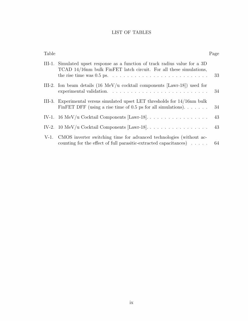
LIST OF TABLES
Table Page
III-1. Simulated upset response as a function of track radius value for a 3DTCAD 14/16nm bulk FinFET latch circuit. For all these simulations,the rise time was 0.5 ps. . . . . . . . . . . . . . . . . . . . . . . . . . . 33
III-2. Ion beam details (16 MeV/u cocktail components [Lawr-18]) used forexperimental validation. . . . . . . . . . . . . . . . . . . . . . . . . . . 34
III-3. Experimental versus simulated upset LET thresholds for 14/16nm bulkFinFET DFF (using a rise time of 0.5 ps for all simulations). . . . . . . 34
IV-1. 16 MeV/u Cocktail Components [Lawr-18]. . . . . . . . . . . . . . . . . 43
IV-2. 10 MeV/u Cocktail Components [Lawr-18]. . . . . . . . . . . . . . . . . 43
V-1. CMOS inverter switching time for advanced technologies (without ac-counting for the effect of full parasitic-extracted capacitances) . . . . . 64
ix

LIST OF FIGURES
Figure Page
I-1. Intel 22nm tri-gate transistors [Auth-12, Seif-12]. As shown in this figure,the metal gate extends upwards from the substrate and wraps aroundthe channel region. In addition, the channel region connects the sourceand drain fins of the FinFET. . . . . . . . . . . . . . . . . . . . . . . . 3
I-2. (a) A comparison of planar and tri-gate transistors. As shown in thisfigure, the FinFET includes a substrate (i.e., silicon wafer) and a metalgate, which extends upwards from the substrate. The metal gate alsowraps around a channel region, which connects the source and drain finsof the FinFET. Shallow trench isolation (STI) regions are formed on orin the substrate on either side of the metal gate. (b) Intel's FinFETtechnology scaling from 22nm tri-gate to 14nm tri-gate transistor. As itcan be seen in this figure, the change from planar transistor structure to3D tri-gate transistor structure impacts the sensitive charge collectionvolume of tri-gate devices [Seif-15b]. . . . . . . . . . . . . . . . . . . . . 4
II-1. Motion of trapped charged particles in the Earth's magnetosphere [Stas-88]. . . . . . . . . . . . . . . . . . . . . . . . . . . . . . . . . . . . . . . 8
II-2. A depiction of Earth's Van Allen radiation belts. Normally only two VanAllen belts (enhancements of charged particles as in the upper panel) aretrapped in Earth's magnetosphere. However, in September 2012, sensorsaboard NASA spacecraft also recorded a third belt (shown in the lowerpanel of this figure) [Beat-13]. . . . . . . . . . . . . . . . . . . . . . . . 9
II-3. Proton and electron domains and boundaries within the two primaryVan Allen belts [Stas-88]. . . . . . . . . . . . . . . . . . . . . . . . . . . 10
II-4. Contour plot of proton fluxes > 10 MeV in the SAA at a 500 km altitudeduring solar maximum [Xaps-06]. . . . . . . . . . . . . . . . . . . . . . 11
II-5. The largest solar flare ever recorded in the radiation effects history ascaptured by the SOHO satellite [Nasa-18]. . . . . . . . . . . . . . . . . 13
II-6. Example curve for LET as a function of depth for a 210-MeV chlorineion in silicon. As shown in this figure, ion LET decreases drasticallyafter the Bragg peak [Dodd-99]. . . . . . . . . . . . . . . . . . . . . . . 15
II-7. (a) – (c) Charge generation and collection processes in a reverse biasedp-n junction and (d) typical shape of the resultant SET/SEU currentrecorded at the junction. The total collected charge corresponds to thearea under the current curve [Mess-82, Baum-05]. . . . . . . . . . . . . 16
x
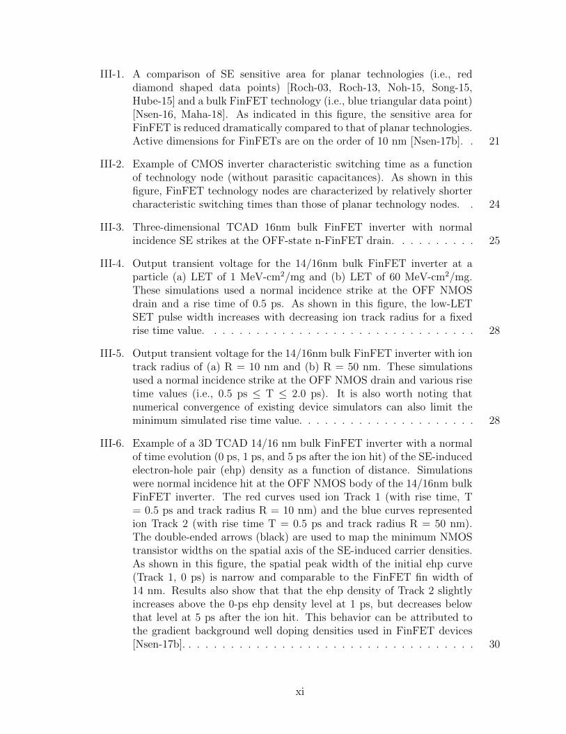
III-1. A comparison of SE sensitive area for planar technologies (i.e., reddiamond shaped data points) [Roch-03, Roch-13, Noh-15, Song-15,Hube-15] and a bulk FinFET technology (i.e., blue triangular data point)[Nsen-16, Maha-18]. As indicated in this figure, the sensitive area forFinFET is reduced dramatically compared to that of planar technologies.Active dimensions for FinFETs are on the order of 10 nm [Nsen-17b]. . 21
III-2. Example of CMOS inverter characteristic switching time as a functionof technology node (without parasitic capacitances). As shown in thisfigure, FinFET technology nodes are characterized by relatively shortercharacteristic switching times than those of planar technology nodes. . 24
III-3. Three-dimensional TCAD 16nm bulk FinFET inverter with normalincidence SE strikes at the OFF-state n-FinFET drain. . . . . . . . . . 25
III-4. Output transient voltage for the 14/16nm bulk FinFET inverter at aparticle (a) LET of 1 MeV-cm2/mg and (b) LET of 60 MeV-cm2/mg.These simulations used a normal incidence strike at the OFF NMOSdrain and a rise time of 0.5 ps. As shown in this figure, the low-LETSET pulse width increases with decreasing ion track radius for a fixedrise time value. . . . . . . . . . . . . . . . . . . . . . . . . . . . . . . . 28
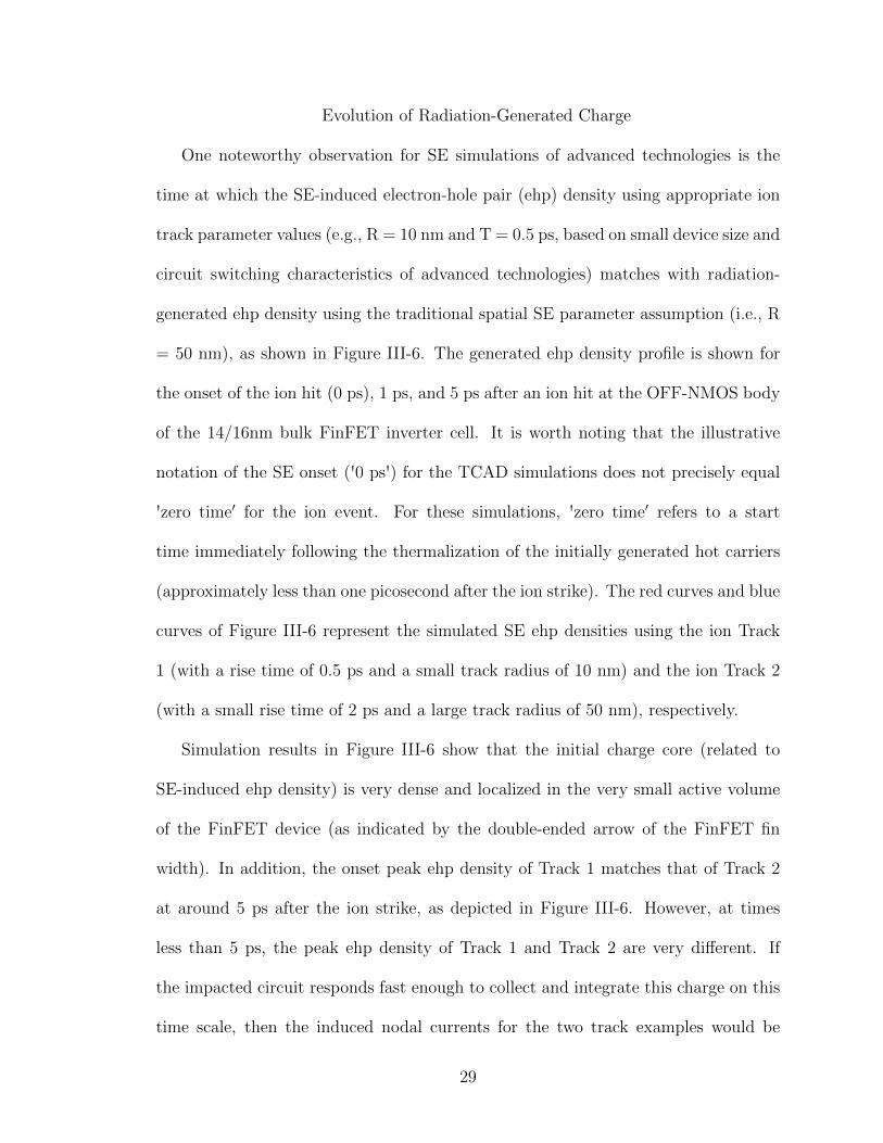
III-5. Output transient voltage for the 14/16nm bulk FinFET inverter with iontrack radius of (a) R = 10 nm and (b) R = 50 nm. These simulationsused a normal incidence strike at the OFF NMOS drain and various risetime values (i.e., 0.5 ps ≤ T ≤ 2.0 ps). It is also worth noting thatnumerical convergence of existing device simulators can also limit theminimum simulated rise time value. . . . . . . . . . . . . . . . . . . . . 28
III-6. Example of a 3D TCAD 14/16 nm bulk FinFET inverter with a normalof time evolution (0 ps, 1 ps, and 5 ps after the ion hit) of the SE-inducedelectron-hole pair (ehp) density as a function of distance. Simulationswere normal incidence hit at the OFF NMOS body of the 14/16nm bulkFinFET inverter. The red curves used ion Track 1 (with rise time, T= 0.5 ps and track radius R = 10 nm) and the blue curves representedion Track 2 (with rise time T = 0.5 ps and track radius R = 50 nm).The double-ended arrows (black) are used to map the minimum NMOStransistor widths on the spatial axis of the SE-induced carrier densities.As shown in this figure, the spatial peak width of the initial ehp curve(Track 1, 0 ps) is narrow and comparable to the FinFET fin width of14 nm. Results also show that that the ehp density of Track 2 slightlyincreases above the 0-ps ehp density level at 1 ps, but decreases belowthat level at 5 ps after the ion hit. This behavior can be attributed tothe gradient background well doping densities used in FinFET devices[Nsen-17b]. . . . . . . . . . . . . . . . . . . . . . . . . . . . . . . . . . . 30
xi
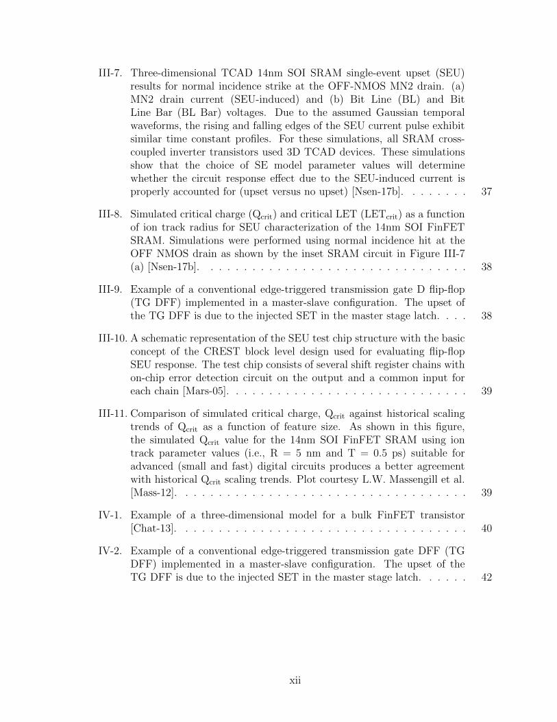
III-7. Three-dimensional TCAD 14nm SOI SRAM single-event upset (SEU)results for normal incidence strike at the OFF-NMOS MN2 drain. (a)MN2 drain current (SEU-induced) and (b) Bit Line (BL) and BitLine Bar (BL Bar) voltages. Due to the assumed Gaussian temporalwaveforms, the rising and falling edges of the SEU current pulse exhibitsimilar time constant profiles. For these simulations, all SRAM cross-coupled inverter transistors used 3D TCAD devices. These simulationsshow that the choice of SE model parameter values will determinewhether the circuit response effect due to the SEU-induced current isproperly accounted for (upset versus no upset) [Nsen-17b]. . . . . . . . 37
III-8. Simulated critical charge (Qcrit) and critical LET (LETcrit) as a functionof ion track radius for SEU characterization of the 14nm SOI FinFETSRAM. Simulations were performed using normal incidence hit at theOFF NMOS drain as shown by the inset SRAM circuit in Figure III-7(a) [Nsen-17b]. . . . . . . . . . . . . . . . . . . . . . . . . . . . . . . . 38
III-9. Example of a conventional edge-triggered transmission gate D flip-flop(TG DFF) implemented in a master-slave configuration. The upset ofthe TG DFF is due to the injected SET in the master stage latch. . . . 38
III-10. A schematic representation of the SEU test chip structure with the basicconcept of the CREST block level design used for evaluating flip-flopSEU response. The test chip consists of several shift register chains withon-chip error detection circuit on the output and a common input foreach chain [Mars-05]. . . . . . . . . . . . . . . . . . . . . . . . . . . . . 39
III-11. Comparison of simulated critical charge, Qcrit against historical scalingtrends of Qcrit as a function of feature size. As shown in this figure,the simulated Qcrit value for the 14nm SOI FinFET SRAM using iontrack parameter values (i.e., R = 5 nm and T = 0.5 ps) suitable foradvanced (small and fast) digital circuits produces a better agreementwith historical Qcrit scaling trends. Plot courtesy L.W. Massengill et al.[Mass-12]. . . . . . . . . . . . . . . . . . . . . . . . . . . . . . . . . . . 39
IV-1. Example of a three-dimensional model for a bulk FinFET transistor[Chat-13]. . . . . . . . . . . . . . . . . . . . . . . . . . . . . . . . . . . 40
IV-2. Example of a conventional edge-triggered transmission gate DFF (TGDFF) implemented in a master-slave configuration. The upset of theTG DFF is due to the injected SET in the master stage latch. . . . . . 42
xii
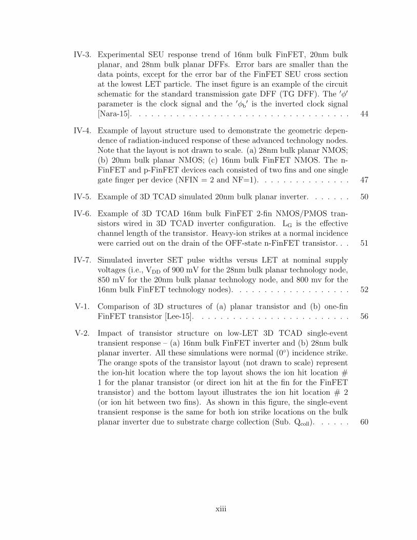
IV-3. Experimental SEU response trend of 16nm bulk FinFET, 20nm bulkplanar, and 28nm bulk planar DFFs. Error bars are smaller than thedata points, except for the error bar of the FinFET SEU cross sectionat the lowest LET particle. The inset figure is an example of the circuitschematic for the standard transmission gate DFF (TG DFF). The ′φ′
parameter is the clock signal and the ′φb′ is the inverted clock signal
[Nara-15]. . . . . . . . . . . . . . . . . . . . . . . . . . . . . . . . . . . 44
IV-4. Example of layout structure used to demonstrate the geometric depen-dence of radiation-induced response of these advanced technology nodes.Note that the layout is not drawn to scale. (a) 28nm bulk planar NMOS;(b) 20nm bulk planar NMOS; (c) 16nm bulk FinFET NMOS. The n-FinFET and p-FinFET devices each consisted of two fins and one singlegate finger per device (NFIN = 2 and NF=1). . . . . . . . . . . . . . . 47
IV-5. Example of 3D TCAD simulated 20nm bulk planar inverter. . . . . . . 50
IV-6. Example of 3D TCAD 16nm bulk FinFET 2-fin NMOS/PMOS tran-sistors wired in 3D TCAD inverter configuration. LG is the effectivechannel length of the transistor. Heavy-ion strikes at a normal incidencewere carried out on the drain of the OFF-state n-FinFET transistor. . . 51
IV-7. Simulated inverter SET pulse widths versus LET at nominal supplyvoltages (i.e., VDD of 900 mV for the 28nm bulk planar technology node,850 mV for the 20nm bulk planar technology node, and 800 mv for the16nm bulk FinFET technology nodes). . . . . . . . . . . . . . . . . . . 52
V-1. Comparison of 3D structures of (a) planar transistor and (b) one-finFinFET transistor [Lee-15]. . . . . . . . . . . . . . . . . . . . . . . . . 56
V-2. Impact of transistor structure on low-LET 3D TCAD single-eventtransient response – (a) 16nm bulk FinFET inverter and (b) 28nm bulkplanar inverter. All these simulations were normal (0◦) incidence strike.The orange spots of the transistor layout (not drawn to scale) representthe ion-hit location where the top layout shows the ion hit location #1 for the planar transistor (or direct ion hit at the fin for the FinFETtransistor) and the bottom layout illustrates the ion hit location # 2(or ion hit between two fins). As shown in this figure, the single-eventtransient response is the same for both ion strike locations on the bulkplanar inverter due to substrate charge collection (Sub. Qcoll). . . . . . 60
xiii
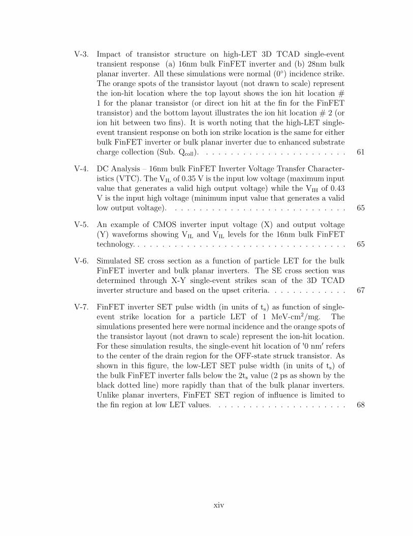
V-3. Impact of transistor structure on high-LET 3D TCAD single-eventtransient response (a) 16nm bulk FinFET inverter and (b) 28nm bulkplanar inverter. All these simulations were normal (0◦) incidence strike.The orange spots of the transistor layout (not drawn to scale) representthe ion-hit location where the top layout shows the ion hit location #1 for the planar transistor (or direct ion hit at the fin for the FinFETtransistor) and the bottom layout illustrates the ion hit location # 2 (orion hit between two fins). It is worth noting that the high-LET single-event transient response on both ion strike location is the same for eitherbulk FinFET inverter or bulk planar inverter due to enhanced substratecharge collection (Sub. Qcoll). . . . . . . . . . . . . . . . . . . . . . . . 61
V-4. DC Analysis – 16nm bulk FinFET Inverter Voltage Transfer Character-istics (VTC). The VIL of 0.35 V is the input low voltage (maximum inputvalue that generates a valid high output voltage) while the VIH of 0.43V is the input high voltage (minimum input value that generates a validlow output voltage). . . . . . . . . . . . . . . . . . . . . . . . . . . . . 65
V-5. An example of CMOS inverter input voltage (X) and output voltage(Y) waveforms showing VIL and VIL levels for the 16nm bulk FinFETtechnology. . . . . . . . . . . . . . . . . . . . . . . . . . . . . . . . . . . 65
V-6. Simulated SE cross section as a function of particle LET for the bulkFinFET inverter and bulk planar inverters. The SE cross section wasdetermined through X-Y single-event strikes scan of the 3D TCADinverter structure and based on the upset criteria. . . . . . . . . . . . . 67
V-7. FinFET inverter SET pulse width (in units of ts) as function of single-event strike location for a particle LET of 1 MeV-cm2/mg. Thesimulations presented here were normal incidence and the orange spots ofthe transistor layout (not drawn to scale) represent the ion-hit location.For these simulation results, the single-event hit location of '0 nm′ refersto the center of the drain region for the OFF-state struck transistor. Asshown in this figure, the low-LET SET pulse width (in units of ts) ofthe bulk FinFET inverter falls below the 2ts value (2 ps as shown by theblack dotted line) more rapidly than that of the bulk planar inverters.Unlike planar inverters, FinFET SET region of influence is limited tothe fin region at low LET values. . . . . . . . . . . . . . . . . . . . . . 68
xiv
V-8. FinFET inverter SET pulse width (in units of ts) as function of single-event strike location for a particle LET of 60 MeV-cm2/mg. Thesimulations presented here were normal incidence and the orange spots ofthe transistor layout (not drawn to scale) represent the ion-hit location.For these simulation results, the single-event hit location of '0 nm′ refersto the center of the drain region for the OFF-state struck transistor. Asshown in this figure, the high-LET SET pulse width (in units of ts) ofthe bulk FinFET inverter crosses the 2ts (2 ps as shown by the blackdotted line) approximately the same way as the SET pulse width (inunits of ts) of the bulk planar inverters. These results show that high-LET SET region of influence is larger than the drawn active region forboth FinFET and planar technologies. . . . . . . . . . . . . . . . . . . 70
V-9. A comparison of (a) calculated flip-flop SE cross sections and (b)experimental SE cross sections for advanced planar and FinFET D flip-flops [Nsen-16]. The calculated SE cross section was computed usingthe simulated SE cross section per inverter (normalized to the drawndrain area of the minimum size NMOS transistor) and the technologylogic area scaling of 0.49 per technology. As shown in this figure, low-LET FinFET SE cross section shows a divergence from simple geometricscaling (Moore's Law) predictions indicated by the black solid curve. . 72
VI-1. (a) Diagram of tilt and roll strikes on a 2-fin bulk FinFET. For a roll angleincidence of 90◦, the ion tilt direction is parallel to the fins while the iontilt direction is perpendicular to the fins for a roll angle of 0◦. (b) Angularupset measurements on 14/16nm bulk FinFET DFFs show SEU crosssection as a function of tilt angle at a 90◦ roll and at 0◦ roll angle. Thisplot demonstrates the strong geometrical and orientation effects, due tothe structure of bulk FinFET devices, on SEU cross-section response.This work elucidates and explains the mechanisms involved in this SEUresponse. . . . . . . . . . . . . . . . . . . . . . . . . . . . . . . . . . . . 78
VI-2. (a) Example of 3D view and (b) 2D cross section view for a 2-fin bulkFinFET structure. Tfin is the top fin width and TS is the bottom finwidth. Hfin is the fin height, Xf the spacing between the nearest edges ofthe two fins, and XS is the spacing between the nearest edges of the twosub-fin structures. . . . . . . . . . . . . . . . . . . . . . . . . . . . . . . 80
xv
VI-3. Geometric analyses of charge deposition mechanisms as a function of tiltangle in 14/16nm bulk FinFETs at a fixed 0◦ roll angle. Four differentcharge deposition mechanisms are at play for this 0◦ roll angle – (a)Mechanism (1): Fin/sub-fin Qdep; (b) Mechanism (2): Reduced fin/sub-fin Qdep. The angle β is an intermediate angle used to calculate θ2;(c) Mechanism (3): 2-fin Qdep and further reduced sub-fin Qdep. Theangle α is an intermediate angle used to calculate θ3; (d) Mechanism(4): 2-fin Qdep, but no sub-fin Qdep. The angular distributions for thesemechanisms are (a) Mechanism (1): 0◦ ≤ θ ≤ 20◦; (b) Mechanism (2):20◦ ≤ θ ≤ 50◦; (c) Mechanism (3): 50◦ ≤ θ ≤ 65◦; and (d) Mechanism(4): θ ≥ 65◦. . . . . . . . . . . . . . . . . . . . . . . . . . . . . . . . . . 83
VI-4. (a) 3D view of a bulk FinFET showing the cut line. (b) 2D cross sectionview of the bulk FinFET. Charge deposition mechanisms for 90◦ rollangle. The 90◦ roll charge chord length continuously increases with tiltangle. . . . . . . . . . . . . . . . . . . . . . . . . . . . . . . . . . . . . 84
VI-5. Simulated SEU results for angled strikes on a full 3D TCAD 14/16nmbulk FinFET (2-fin) latch at a fixed 0◦ roll angle and VDD of 0.65 V. Theblue-colored doping concentration of the 2D Qdep profiles corresponds tothe intrinsic doping concentration of the simulated bulk FinFET. Asshown in this figure, simulated angular upset responses correlate withangular SE mechanisms elucidated by the developed geometric analysis[Nsen-18]. . . . . . . . . . . . . . . . . . . . . . . . . . . . . . . . . . . 86
VI-6. The IC test structure used for angular irradiations. (a) The IC testprinted circuit board (PCB) showing no obstructions to beam path, forhigh tilt angles of incidence from the top and left edges of the PCB. TheTeensy 3.2 microcontroller board is visible on the right edge of the PCB.(b) A picture of the test chip elevated on gold spacers with bond wires ononly two sides of the die. The DUT was packaged on gold plate spacers,which placed the DUT above the edge of the package cavity, providingan unobstructed path on two sides for the ion beam at high tilt anglesof incidence [Kaup-18]. . . . . . . . . . . . . . . . . . . . . . . . . . . . 88
VI-7. High-LET 0◦ roll SEU cross section per FF as a function of tilt angle.As shown in this figure, the upset cross section as a function of incidenttilt angle does not change significantly from normal incidence up to 80◦.The slight decrease in upset cross section from around 60◦ is attributedto coupled mechanisms (3) & (4). At around 85◦, the distance throughthe metallization overlayers is on the order of the ions penetration rangelimiting the number of ions reaching the active silicon, which results ina reduced SEU cross section measured at the 85◦ tilt angle. . . . . . . . 89
xvi

VI-8. Low-LET 0◦ roll SEU cross section per FF as a function of tilt angleand a fixed 0◦ roll angle at VDD = 0.65 V and a particle LET of 1 MeV-cm2/mg. The SEU cross section is the highest at normal incidence andstarts to decrease at around 20◦ due to mechanism (2). However, ataround 50◦, the SEU cross section starts to increase again due to strikeon two fins according to mechanism (3). At around 65◦, the SEU crosssection decreases due to mechanism (4), which is characterized by chargedeposition in two fins, but no charge deposition in the sub-fin region. . 92
VI-9. Normalized charge chord length as a function of tilt angle (with a fixed0◦ roll angle) for the 14/16nm bulk FinFET in the angular region (3).Calculated chord lengths in this figure are normalized to the chord lengthvalue at 65◦ tilt angle. . . . . . . . . . . . . . . . . . . . . . . . . . . . 93
VI-10. Inverter FWHM SET pulse width as a function of tilt angle and a fixed0◦ roll angle for the angular region (3). These SET results were obtainedfrom 3D TCAD simulations of the 14/16nm bulk FinFET inverter for aparticle LET of 1 MeV-cm2/mg. For these SET results, VDD was 0.65V and the ion hit occurred at the drain of the OFF NMOS transistor ofthe simulated full 3D inverter structure. . . . . . . . . . . . . . . . . . 94
VI-11. High-LET 90◦ roll SEU cross section per FF as a function of tilt angle.As shown in this figure, the high-LET SEU cross section does notchange significantly across tilt angles, consistent with the observationand mechanisms discussed in the fixed 0◦ roll angle case, shown in FigureVI-7. . . . . . . . . . . . . . . . . . . . . . . . . . . . . . . . . . . . . . 95
VI-12. Low-LET 90◦ roll SEU cross section per FF as a function of tilt angle. Asshown in this figure, low-LET 90◦ roll angle upset cross section increaseswith tilt angle due to an increase in charge chord length in the active Siregion of the bulk FinFET. . . . . . . . . . . . . . . . . . . . . . . . . . 96
VI-13. Impact of bias on angular alpha FF upset cross sections as function oftilt angle. (a) Effect of bias on 0◦ roll FF SEU cross section. (b) Effectof bias on 90◦ roll FF SEU cross section. As shown in both figures (a) &(b), SEU cross section dependence on tilt angle decreases with reducedvoltage supply due to reduced critical charge, Qcrit. In addition, SEUcross section at one tilt angle of incidence increases with reduced supplyvoltage. This increase in SEU cross section per FF is attributed to anincrease in SET pulse width at a reduced supply voltage [Nsen-16]. . . 98
xvii

CHAPTER I
INTRODUCTION
Since the prediction of space-system upsets from ionizing particles by Wallmark
and Marcus [Wall-62] and the first report of experimentally observed upsets in
communication satellites by Binder et al. in 1975 [Bind-75], single-event effects (SEE)
have been an increasing concern for the reliable operation of space, military, and
ground-based electronic applications. The SEE occurrence is a random and localized
phenomenon due to the interaction of a highly energetic ionizing particle with circuit
materials. Generally, the result of a single event (SE) on the impacted circuit ranges
from the generation of a transient photocurrent/voltage pulse to the corruption of
data stored in struck memory elements. The SE-induced transient signal is typically
referred to as a single-event transient (SET) if it affects a combinational logic circuit,
whereas a single-event upset (SEU) occurs within a memory circuit element. However,
if a SET is latched by a memory element (e.g., D latch, flip-flop, register files, etc.),
then it is also treated as an upset (i.e., SEU) to the memory circuit.
For advanced integrated circuits (ICs), the increased susceptibility to SEE is
primarily attributed to factors associated with device scaling trends [John-98, Nsen-
16]. For example, some of these scaling factors include reduced transistor feature sizes,
higher packing densities, increased operating frequencies, and the change from planar
transistor structure to three-dimensional (3D) multi-gate transistor structure (e.g., fin
field-effect transistor or FinFET) [Seif-12, Seif-15b, Nsen-16, Zhan-17]. A depiction
of the 3D tri-gate transistors (FinFETs) is shown in Figure I-1 [Auth-12, Seif-12]
1
and Figure I-2 [Seif-15b]. It is also worth mentioning that the change from planar
transistor structure to FinFET structure was motivated by the enhanced electrostatic
control from multiple gates and reduction in short-channel effects (SCEs) of FinFETs
compared to planar transistors.
However, while SE-induced mechanisms in planar complementary metal-oxide
semiconductor (CMOS) technologies are well understood, the structural modifications
associated with moving from planar transistors to FinFETs introduce new considera-
tions in terms of charge collection processes and SE sensitive area of FinFET circuits.
Thus, it is important to investigate the impact of FinFET transistor structure on SEE
response/mechanisms of FinFET based memory circuits used in both space-deployed
and terrestrial electronics applications.
The objective of this work is to fully characterize and quantify the impact of the
CMOS FinFET structure on physical SEU mechanisms and experimentally observed
SEU responses of bulk FinFET technologies. Both 3D technology computer-aided
design (TCAD) device simulations and experimental testing are used to study SE
failure mechanisms and upset error signatures in advanced bulk planar circuits and
bulk FinFET circuits. In order to fully understand the mechanisms that affect SE
responses in bulk FinFET technologies, this work examines a wide range of advanced
technologies, ranging from 28nm bulk planar technology node down to 16/14nm bulk
FinFET technology nodes.
In addition to experimental testing, circuit simulations also play an important role
in the SE characterization of any given technology node [Rain-14, Hazu-00, Lin-14,
Mars-05]. With technology scaling below 22 nm and circuit response times below 10
ps, the spatial and temporal model parameter values assumed when simulating device-
2
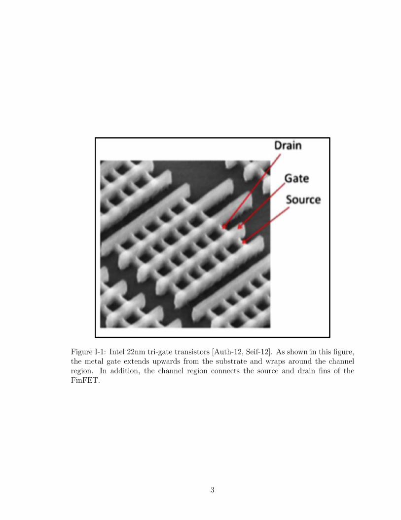
Figure I-1: Intel 22nm tri-gate transistors [Auth-12, Seif-12]. As shown in this figure,the metal gate extends upwards from the substrate and wraps around the channelregion. In addition, the channel region connects the source and drain fins of theFinFET.
3
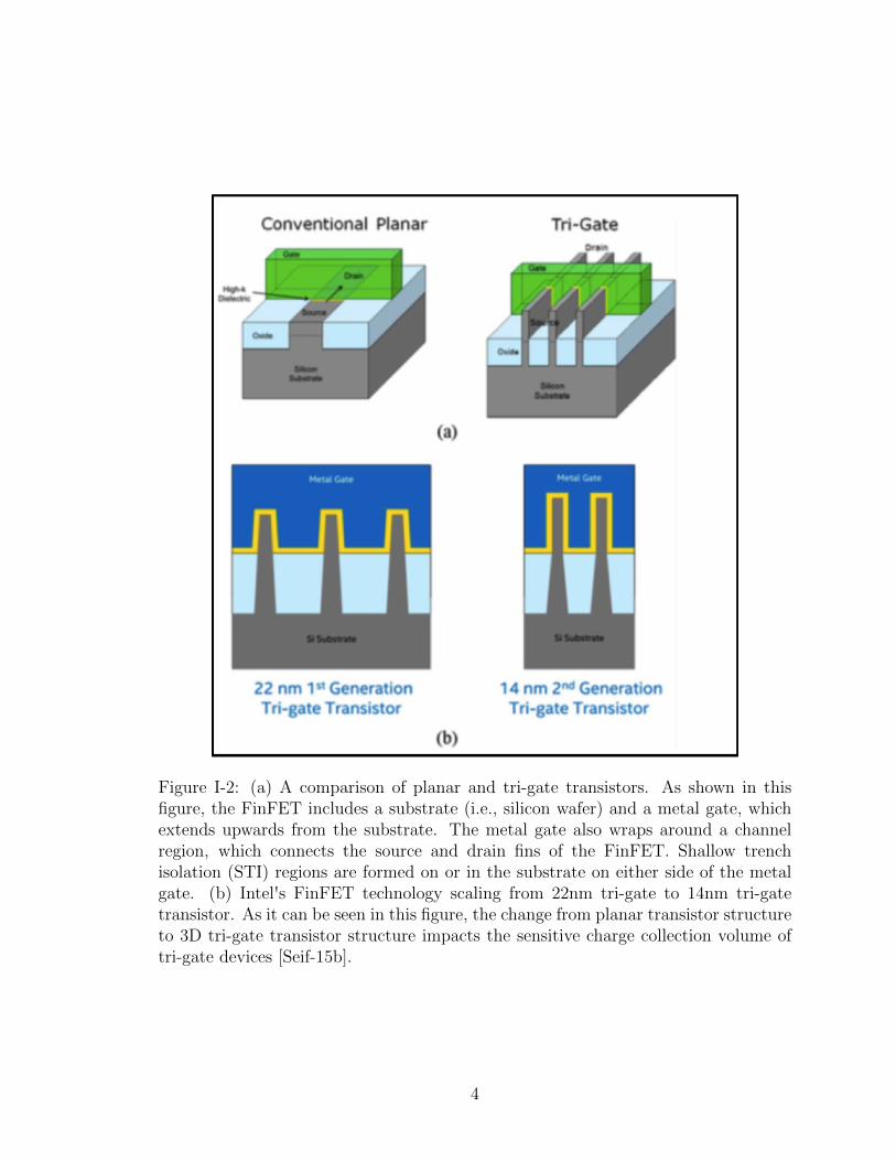
Figure I-2: (a) A comparison of planar and tri-gate transistors. As shown in thisfigure, the FinFET includes a substrate (i.e., silicon wafer) and a metal gate, whichextends upwards from the substrate. The metal gate also wraps around a channelregion, which connects the source and drain fins of the FinFET. Shallow trenchisolation (STI) regions are formed on or in the substrate on either side of the metalgate. (b) Intel's FinFET technology scaling from 22nm tri-gate to 14nm tri-gatetransistor. As it can be seen in this figure, the change from planar transistor structureto 3D tri-gate transistor structure impacts the sensitive charge collection volume oftri-gate devices [Seif-15b].
4
and circuit-level SE response using 3D TCAD simulations also show a significant
impact on the simulation results. Therefore, this work also investigates the sensitivity
of the simulation results to the choice of model parameter values, and appropriately
reflects the physics of the ion-induced charge-generation process in the choice of
parameters.
Additionally, novel SE analysis techniques and upset criteria for effectively
bridging transistor-level SE response to circuit-level upset cross section response
of advanced technologies are also developed. Moreover, angular effects (e.g., low-
and high-angle ion incidences) on FinFET SE mechanisms and SE responses are
characterized. Angular SE analyses are of utmost importance for these small-volume
geometry technologies (i.e., FinFETs) in order to (1) account for the effect of the
omnidirectional radiation space environment, (2) provide the basis for worst-case test
conditions, and (3) accurately predict soft error rates (SER) of bulk FinFET designs.
Dissertation Organization
The research work presented in this dissertation is organized as follows:
1) Chapter I introduces the motivation and organization of this work.
2) Chapter II provides a background on radiation effects including radiation
environments and single-event effects on digital electronic circuits. Charge generation
and charge collection mechanisms for SE responses are also discussed.
3) Chapter III presents new spatial and temporal considerations for analysis of
SE responses/mechanisms in sub-22nm technologies. This work is an expansion of
the study presented in [Nsen-17b]. In this work, sensitivity studies are carried out in
order to understand the sensitivity of the simulation results to the choice of model
5
parameter values, and to appropriately reflect the physics of the ion-induced charge-
generation process in the choice of parameters.
4) Chapter IV presents a comparative study of SEU cross section response trends
of advanced bulk planar and bulk FinFET technologies. This work describes and
extends the research study in [Nsen-16].
5) Chapter V investigates and quantifies bulk FinFET structural effects on SE
cross sections. This work is an expansion of the study in [Nsen-17a].
6) Chapter VI characterizes angular effects on SE mechanisms in bulk FinFET
technologies. This work is an expansion of the research in [Nsen-18]. Through
a thorough characterization of unique geometric and orientation SEE dependences
of discrete FinFET structure, novel angular upset mechanisms are also discovered
and discussed in this work. The analysis of these failure mechanisms enables risk
reduction in radiation hardened by design (RHBD) design and allows accurate error
rate calculations of terrestrial and defense/space applications.
7) Chapter VII provides some concluding remarks regarding the presented
research. The impact of this work on the radiation effects community is also presented.
6
CHAPTER II
RADIATION EFFECTS BACKGROUND
Electronic circuits are exposed to various radiation environments on earth and in
space. The exposure of electronics to radiation can lead to temporary perturbations
or permanent damage of semiconductor devices. Examples of radiation effects on
electronics include total-ionizing dose (TID), prompt dose (dose rate), displacement
damage (DD), and single-event effects (SEE). This chapter provides an overview
of radiation environments and the study of radiation effects on electronics circuits,
especially those of particular pertinence to the research presented in this work (i.e.,
SEE).
Radiation Environments
Both natural space and terrestrial radiation environments pose a reliability
concern for electronics ICs. The atmospheric radiation environment consists of non-
ionizing particles (e.g., neutrons) and ionizing particles (e.g., protons, heavy ions,
muons, etc.). The natural space radiation environment is most complex and dynamic
and will be the focus of this section. The space environment consists of a variety of
energetic particles with energies ranging from KeV to GeV and beyond. The main
contributors to space radiation environments are trapped particles, cosmic rays, and
solar flares.
7

Trapped Radiation Environment
This radiation environment consists of a broad spectrum of energetic particles
that are trapped by the Earth's magnetic field. The charged particles in this
field follow relatively reliable trajectories and move in a spiral fashion around the
magnetic field lines, tightening as they approach the magnetic poles where the field
strength increases. Eventually the field strength becomes sufficient to compel the
particle to reverse direction, as shown in Figure II-1. In addition, the Earth's
trapping phenomenon leads to an accumulation of particles in specific areas of the
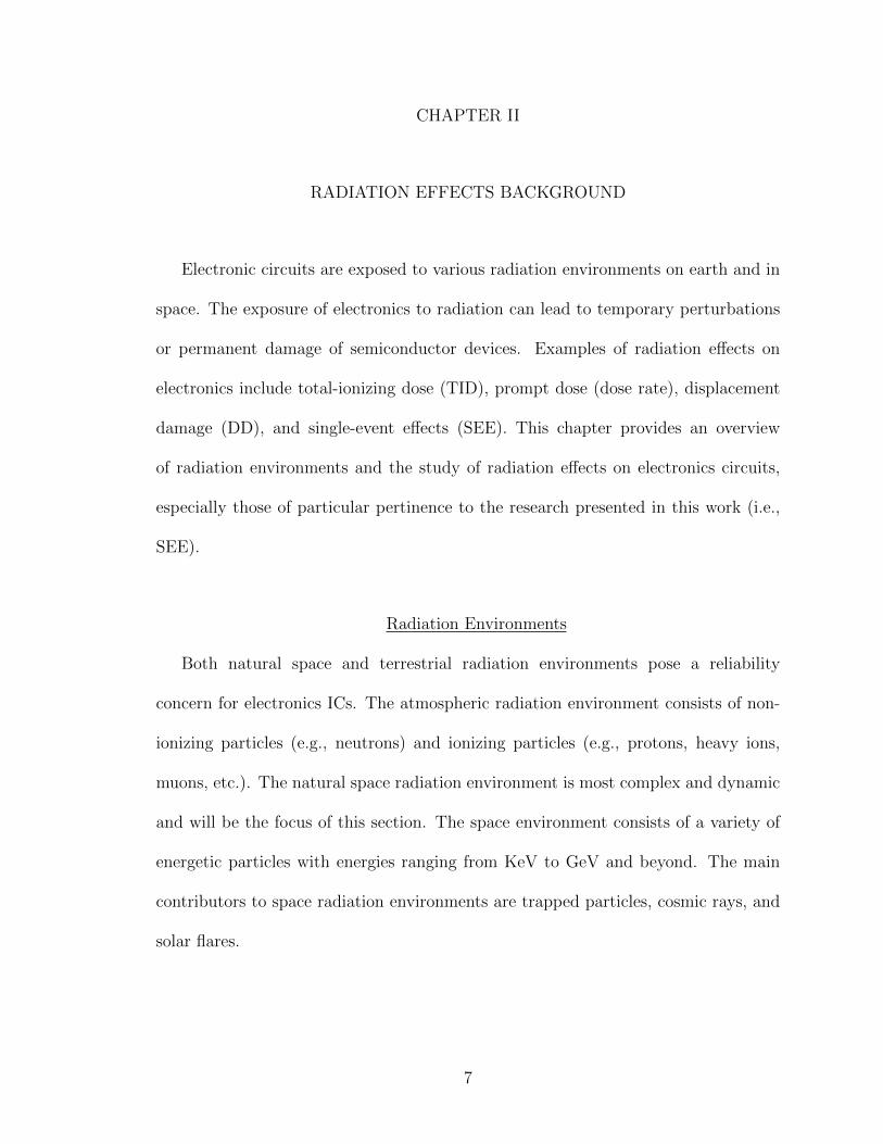
magnetosphere termed the Van Allen radiation belts [Alle-59]. The Van Allen belts
consist of two permanent belts, as shown in Figure II-2 and Figure II-3: (1) an
outer zone centered at approximately 6 Earth radii and (2) an inner zone centered
at approximately 2.5 Earth radii. The outer zone primarily consists of electrons and
some protons trapped from solar flare events, whereas the inner zone is comprised of
protons and some trapped electrons [Stas-88]. Electrons contribute to most radiation
events in the outer zone, whereas protons contribute to the majority of events in the
inner belt [Mazu-02].
Figure II-1: Motion of trapped charged particles in the Earth's magnetosphere [Stas-88].
8

Figure II-2: A depiction of Earth's Van Allen radiation belts. Normally only two VanAllen belts (enhancements of charged particles as in the upper panel) are trappedin Earth's magnetosphere. However, in September 2012, sensors aboard NASAspacecraft also recorded a third belt (shown in the lower panel of this figure) [Beat-13].
9
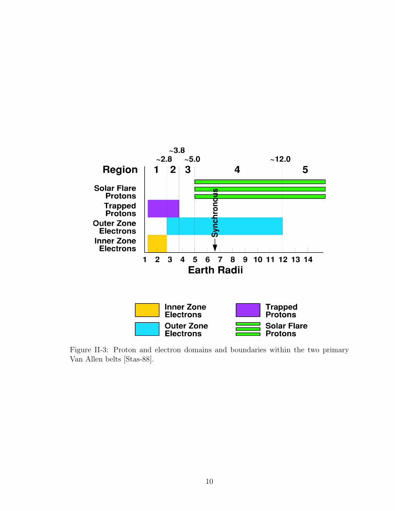
Figure II-3: Proton and electron domains and boundaries within the two primaryVan Allen belts [Stas-88].
10
Coupled with the proton belt is the South Atlantic Anomaly (SAA), shown in
Figure II-4. This anomaly results from the tilt of the Earth's magnetic pole from the
geographic pole and the displacement of the magnetic field from the center, causing
a dip in the Earth's magnetic field over the South Atlantic Ocean. This dip creates
a bulge at the underside of the inner belt [Bart-03], allowing cosmic rays and other
charged particles to reach lower into the atmosphere. The SAA is located off the
coast of South America and displays a large increase in proton flux (> 30 MeV) at
altitudes less than 1000–2000 km [Baze-97], and can cause significant SEE issues for
satellites, aircrafts, and space shuttles operating in the region.
Figure II-4: Contour plot of proton fluxes > 10 MeV in the SAA at a 500 km altitudeduring solar maximum [Xaps-06].
Cosmic Rays
There exist three main sources of cosmic rays: galactic cosmic rays (GCR), solar
cosmic rays (SCR), and terrestrial cosmic rays (TCR). While the exact source of
11
GCRs is still unknown, they are believed to originate somewhere outside of our solar
system and are postulated to be remnants from supernovae (exploding stars). These
GCRs are comprised of most elements of the periodic table with energies ranging
from 109 eV up to 1020 eV [Bird-95]. The composition of these GCRs is estimated
to be 85% protons (hydrogen nuclei), 14% alpha particles (helium nuclei), and 1%
heavy ions.
Solar Particle Events
An additional source of space irradiation is the Sun. Sporadic and rapid bursts
of radiation called solar flares are emitted by the Sun. The largest solar flare ever
recorded occurred on April 2, 2001 and was captured by the Solar and Heliospheric
Observatory (SOHO) satellite, as shown in Figure II-5. The Sun's solar cycle averages
a span of 11 years with 7 years of high activity and 4 years of relative inactivity within
the 11-year solar cycle.
Basic Single-Event Mechanisms
Radiation-induced effects can lead to a variety of device- and circuit-level responses
such as displacement damage (DD), total-ionizing dose (TID), prompt dose (dose
rate), and single-event effects (SEE). This section focuses on basic SEE mechanisms
since they are the most dominant SE failure modes in modern digital circuits (e.g.,
FinFETs) [Seif-15b, Nsen-16].
12
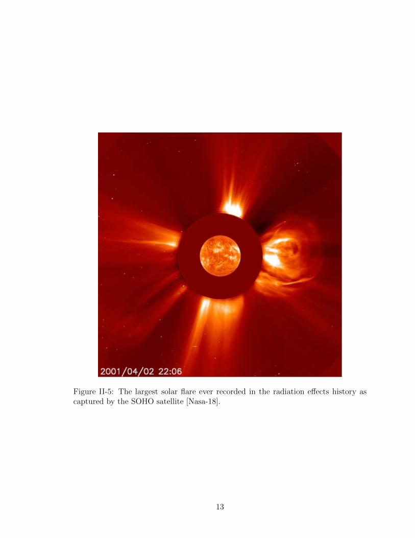
Figure II-5: The largest solar flare ever recorded in the radiation effects history ascaptured by the SOHO satellite [Nasa-18].
13
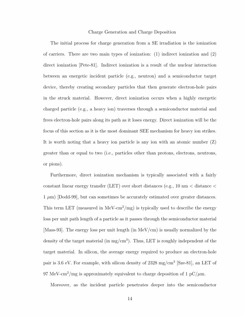
Charge Generation and Charge Deposition
The initial process for charge generation from a SE irradiation is the ionization
of carriers. There are two main types of ionization: (1) indirect ionization and (2)
direct ionization [Pete-81]. Indirect ionization is a result of the nuclear interaction
between an energetic incident particle (e.g., neutron) and a semiconductor target
device, thereby creating secondary particles that then generate electron-hole pairs
in the struck material. However, direct ionization occurs when a highly energetic
charged particle (e.g., a heavy ion) traverses through a semiconductor material and
frees electron-hole pairs along its path as it loses energy. Direct ionization will be the
focus of this section as it is the most dominant SEE mechanism for heavy ion strikes.
It is worth noting that a heavy ion particle is any ion with an atomic number (Z)
greater than or equal to two (i.e., particles other than protons, electrons, neutrons,
or pions).
Furthermore, direct ionization mechanism is typically associated with a fairly
constant linear energy transfer (LET) over short distances (e.g., 10 nm < distance <
1 µm) [Dodd-99], but can sometimes be accurately estimated over greater distances.
This term LET (measured in MeV-cm2/mg) is typically used to describe the energy
loss per unit path length of a particle as it passes through the semiconductor material
[Mass-93]. The energy loss per unit length (in MeV/cm) is usually normalized by the
density of the target material (in mg/cm3). Thus, LET is roughly independent of the
target material. In silicon, the average energy required to produce an electron-hole
pair is 3.6 eV. For example, with silicon density of 2328 mg/cm3 [Sze-81], an LET of
97 MeV-cm2/mg is approximately equivalent to charge deposition of 1 pC/µm.
Moreover, as the incident particle penetrates deeper into the semiconductor
14
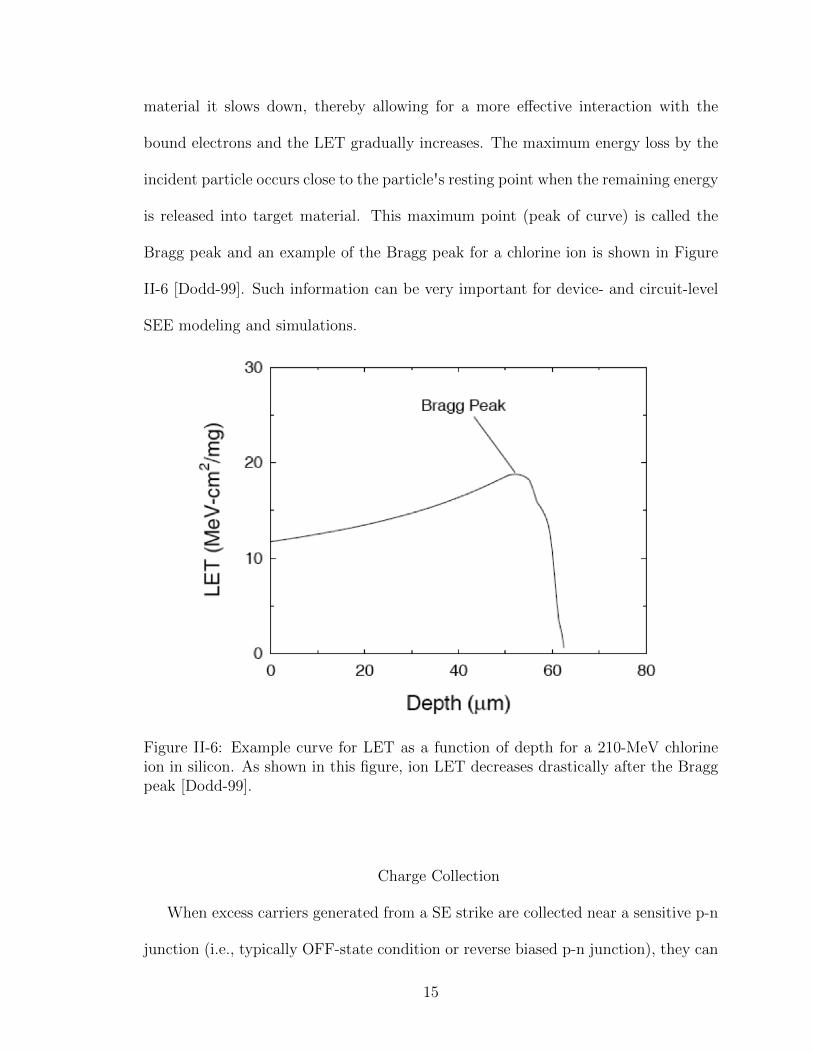
material it slows down, thereby allowing for a more effective interaction with the
bound electrons and the LET gradually increases. The maximum energy loss by the
incident particle occurs close to the particle's resting point when the remaining energy
is released into target material. This maximum point (peak of curve) is called the
Bragg peak and an example of the Bragg peak for a chlorine ion is shown in Figure
II-6 [Dodd-99]. Such information can be very important for device- and circuit-level
SEE modeling and simulations.
Figure II-6: Example curve for LET as a function of depth for a 210-MeV chlorineion in silicon. As shown in this figure, ion LET decreases drastically after the Braggpeak [Dodd-99].
Charge Collection
When excess carriers generated from a SE strike are collected near a sensitive p-n
junction (i.e., typically OFF-state condition or reverse biased p-n junction), they can
15

cause a change in state for the struck circuit. Shown in Figure II-7 are the three main
mechanisms governing the charge collection process: (1) drift – is the charge transport
in response to an applied or a built-in electric field in the device junction depletion
region; (2) diffusion – is the charge transport due to carrier concentration gradients
within the device; and/or (3) recombination – corresponds to the annihilation of two
oppositely charged carriers by recombining with each other.
Figure II-7: (a) – (c) Charge generation and collection processes in a reverse biasedp-n junction and (d) typical shape of the resultant SET/SEU current recorded at thejunction. The total collected charge corresponds to the area under the current curve[Mess-82, Baum-05].
The shape of the radiation-induced current pulse can be related to the dynamics
16
of charge collection (Qcoll) and the resulting current can be expressed as
I(t) =dQcoll
dt(II-1)
where I(t) is the radiation-induced current, Qcoll is the collected charge, and t is the
elapsed time after the onset of the ion hit. It is worth noting that the collected
charge is less than a femtocoulomb for modern technologies [Seif-15b, Nsen-16], and
the drift current can be limited by the saturation velocity of the carriers (e.g., Vsat
107 cm2/s for electrons in silicon). As a result, the resulting transient current in
advanced circuits is typically on the order of picoseconds.
SEE Modeling and Simulation Tools
Device- and circuit-level SE modeling and simulation can provide important
insights into physical upset mechanisms in struck circuits. Typical tools used for SE
modeling and simulation analyses include TCAD (e.g., Synopsys Sentaurus TCAD
tools [Syno-18], Silvaco TCAD tools [Silv-18]), Monte Carlo simulation tools [Tylk-
97, Well-09, Well-10, Rain-11b, Mend-12, Reed-13, Adam-18, Gean-18], and circuit
simulators (e.g., Cadence Virtuoso tools [Cade-18]). It is worth mentioning that
circuit simulators are typically used to simulate more complex circuit designs such
as D flip-flops as TCAD simulations of such complex circuits may require huge
computation resources and extremely long time periods.
Conclusions
This chapter presents an overview of radiation environments that are of par-
ticular concern for SEE analysis of advanced digital circuits. Charge generation
17

and collection mechanisms after an ion hit on a semiconductor material are also
discussed. Existing simulation tools needed for device- and circuit-level SE modeling
for digital circuits are also discussed. The understanding of radiation environments,
charge generation/collection mechanisms, and accurate prediction of error rates is
very important to the mission success of space-deployed and terrestrial electronics
systems.
18
CHAPTER III
SPATIAL AND TEMPORAL CONSIDERATIONS FOR ANALYSIS OF
SINGLE-EVENT MECHANISMS IN FINFET TECHNOLOGIES
The spatial and temporal model parameter values assumed when simulating
device- and circuit-level single-event effects using 3D TCAD have a significant impact
on the simulation results. Characteristic active-region dimensions of modern CMOS
devices are now ≤ 20 nm, and circuit-switching times are below 10 ps. It is important
to understand the sensitivity of the simulation results to the choice of model parameter
values, and to appropriately reflect the physics of the ion-induced charge-generation
process in the choice of parameters.
TCAD SEE Simulations and Device Sensitive Area Trends
As a highly energetic charged particle penetrates through the semiconductor
materials, it produces a large density of electron-hole pairs near the particle trajectory.
The electron-hole pairs created by the incident particle can be collected via drift and
diffusion processes and cause the occurrence of a soft error.
TCAD simulation tools are used to simulate the transient response of electronic
devices to energy (converted to charge) deposited by an ionizing particle in the
semiconductor material regions [Duss-93, Muss-98, Benn-12, Nsen-16]. Typical
models used in TCAD tools to represent the charge generated by an ion are based
upon Gaussian spatial and temporal representations. The Gaussian model and basis
for model parameter values such as the spatial radius of the assumed Gaussian charge
19
track, and the temporal time profile have generally been based upon the assumption
that the charge-generation time (based on the velocity of the ion traversing a sensitive
region) is very short compared to the response time of the devices being studied
[Duss-93, Muss-98]. Depending on the mass and energy of the specific ions, these
assumptions tend to produce very dense initial charge cores along with some number
of secondary electrons having larger ranges [Weed-14]. These fast electrons are the
agents by which the energy of the primary ions is distributed locally around the track
[Koba-04]. It is worth noting that the track evolution process starts much earlier (in
the femtosecond range) as observed in the study of Schiewietz et al. [Schi-04].
The assumed Gaussian spatial distribution for the charge generated by a single
particle can also be thought of as averaging a large number of individual events at
some time after the initial impulse function of the ion strike. This representation
neglects nuclear and secondary-electron events, which can result in discrete reactions
at relatively large distances. Historically, a value of 50 nm has often been assumed
for the characteristic length of the spatial parameter, and a number on the order
of picoseconds for the temporal (rise time) parameter in the single-event charge
generating models used in 3D TCAD simulations [Benn-13, Ferl-05, Arto-10, Hoot-
13]. With technology dimensions well below 50 nm (as shown in Figure III-1), and
circuit response times reduced to well below 10 ps [Nsen-17a], these assumptions
invite re-evaluation. Results in Figure III-1 demonstrate that the relevant region
of influence for sub-22nm devices (i.e., the sensitive area) is much smaller than the
spatial extent of an ion interaction.
In addition, the metrics for characterizing single-event sensitivity of specific digital
circuits include critical charge, Qcrit (the minimum charge required to cause a bit flip
20
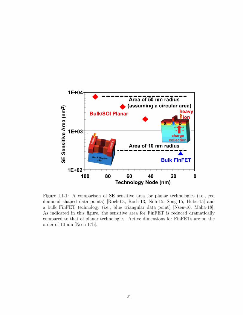
Figure III-1: A comparison of SE sensitive area for planar technologies (i.e., reddiamond shaped data points) [Roch-03, Roch-13, Noh-15, Song-15, Hube-15] anda bulk FinFET technology (i.e., blue triangular data point) [Nsen-16, Maha-18].As indicated in this figure, the sensitive area for FinFET is reduced dramaticallycompared to that of planar technologies. Active dimensions for FinFETs are on theorder of 10 nm [Nsen-17b].
21

in a memory circuit) and SET pulse widths [Mass-93, Baum-05b, Nara-07, Gadl-10].
These values are compared to the perturbations induced by a given ion under given
conditions (bias, strike location, angle of strike, etc.), which are characterized by
collected charge, Qcoll at a node (for which some integration time must be chosen) or
the voltage transient observed at a node. Often, 3D TCAD simulations are performed
on fixed-biased transistors in order to determine the collected charge or the transient
pulse width [Gadl-10, Baum-05a, Baum-05b]. However, with circuit response times
comparable to the charge deposition and collection times, and the spatial extent of
the induced perturbations capable to impact multiple devices simultaneously, it has
become challenging to connect a simulated single-device SE response to circuit upset
response. The dynamic transient loads must also be included in transient simulations.
Increased computational capabilities, along with the use of combined TCAD and
compact-model approaches, have been adopted to address these issues. One of the
key considerations, however, in such simulations is the appropriate representation
of the initial stimulus in the context of sub-22nm device dimensions with sub 10-ps
switching times.
Effects of Ion Track Structure on SE Response
Previous studies have examined the effects of ion track structure on SE response
using different track structure formulations [Kobe-68, Duss-93, Fage-94, Akke-05],
and Monte Carlo simulations [Akke-05, Mura-08, Rain-11a, Rain-12, Weed-14, Rain-
14]. However, these references mainly focus on planar Silicon-On-Insulator (SOI)
technologies (from 1 µm to 24 nm technology nodes [Rain-14]) and SOI FinFET
technologies (e.g., 20nm SOI nanowire FinFET [Rain-14] and 14nm SOI FinFET
22
[Weed-14]). Recent studies of bulk FinFETs indicate that charge deposition/collec-
tion processes, sensitive area (Adiff), and the resulting upset rate of advanced bulk
technologies exhibit a strong dependence on bulk FinFET structure [Nsen-17a]. This
observation is very important as soft error rate (SER) for a given technology depends
exponentially on the ratio of the critical charge (Qcrit) to collected charge (Qcoll)
[Hazu-00]:
SER ∼ Adiff · exp(−Qcrit
Qcoll
) (III-1)
Thus, it is necessary to examine the sensitivity of radiation-generated charge-track
model parameters to transistor structure for highly scaled CMOS technologies.
Characteristic Switching Time Trends
Figure III-2 shows a comparison of CMOS inverter characteristic switching time
values as a function of technology node. The inverter characteristic switching time
is the time required for a valid input signal to propagate through the inverter
gate until it has become a valid output signal (i.e., the time to switch a logic
'0′ to a logic '1′ or vice-versa). These switching time results were obtained using
Cadence SPICE inverter simulations with minimum size transistors designed using
the indicated process nodes (from 130nm planar technology node down to 14/16nm
FinFET technology nodes). As indicated in Figure III-2, the 14/16nm FinFET
technology nodes exhibit relatively shorter characteristic switching times than those
of planar technology nodes. These simulations demonstrate that modern circuit
response times can undercut a conventional ion charge generation Gaussian profile
used in simulation. The important impact of this temporal characteristic parameter
23
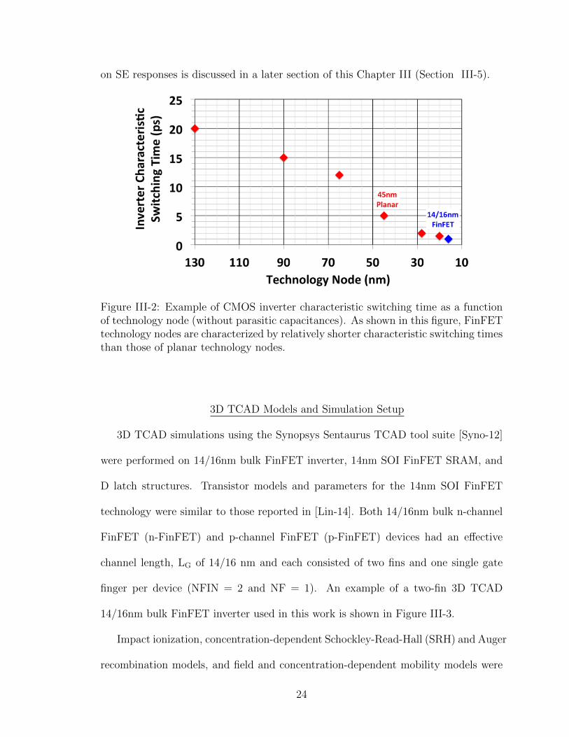
on SE responses is discussed in a later section of this Chapter III (Section III-5).
Figure III-2: Example of CMOS inverter characteristic switching time as a functionof technology node (without parasitic capacitances). As shown in this figure, FinFETtechnology nodes are characterized by relatively shorter characteristic switching timesthan those of planar technology nodes.
3D TCAD Models and Simulation Setup
3D TCAD simulations using the Synopsys Sentaurus TCAD tool suite [Syno-12]
were performed on 14/16nm bulk FinFET inverter, 14nm SOI FinFET SRAM, and
D latch structures. Transistor models and parameters for the 14nm SOI FinFET
technology were similar to those reported in [Lin-14]. Both 14/16nm bulk n-channel
FinFET (n-FinFET) and p-channel FinFET (p-FinFET) devices had an effective
channel length, LG of 14/16 nm and each consisted of two fins and one single gate
finger per device (NFIN = 2 and NF = 1). An example of a two-fin 3D TCAD
14/16nm bulk FinFET inverter used in this work is shown in Figure III-3.
Impact ionization, concentration-dependent Schockley-Read-Hall (SRH) and Auger
recombination models, and field and concentration-dependent mobility models were
24
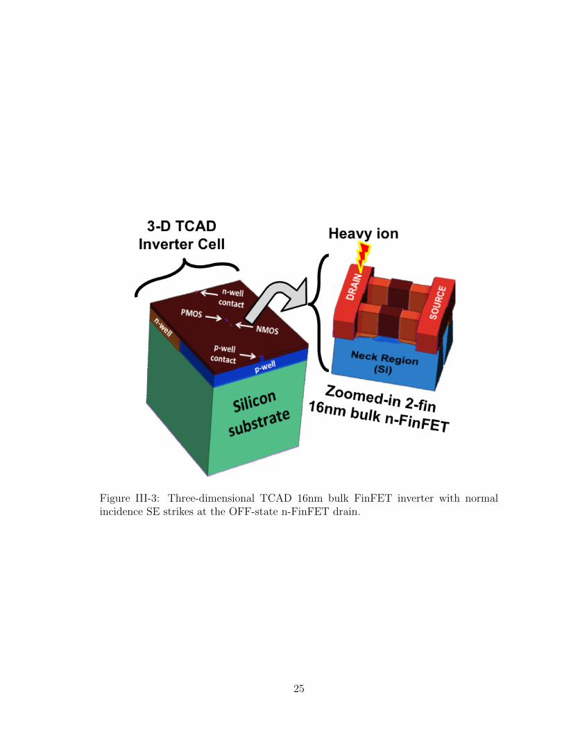
Figure III-3: Three-dimensional TCAD 16nm bulk FinFET inverter with normalincidence SE strikes at the OFF-state n-FinFET drain.
25
also utilized in all simulations. Electrical parameters such as drain current-gate
voltage (ID-VG) drain current-drain-source voltage (ID-VDS) curves for the 16nm
bulk FinFET transistors were calibrated using the Arizona State University (ASU)
14/16nm bulk FinFET Predictive Technology Models (PTM) [Ariz-18]. The particle
LET was converted into SE charge deposition in terms of pC/µm. This conversion
from pC/µm to LET accounts for both the ionization energy and the density of
the material traversed by the particle [Mass-93]. Photogenerated carriers were also
distributed according to a Gaussian function of radius, R. All simulated heavy ion
strikes were at normal incidence and the hit transistor was in the OFF-state condition,
as this is the single-event sensitive state of the device.
3D TCAD SEE Simulation Results
Impact of Ion Track Parameter Choice on Simulated SE Response Predictions
An extensive sensitivity simulation study was carried out using 14/16m bulk
FinFET inverters, 14nm SOI FinFET SRAM, and 14/16nm conventional unhardened
D latch [Ball-18] in order to investigate the sensitivity of SE simulation results to the
choice of SE model parameter values, and to appropriately reflect the physics of
the ion-induced charge-generation process in the choice of parameters. The nominal
supply voltage (i.e., VDD = 800 mV) was used and the assumed Gaussian ion track
radius (denoted, R) values ranged from 5 nm up to 80 nm for all reported simulations
of this work. The rise time (denoted, T) for the Gaussian heavy ion model was varied
between 0.5 ps and 2 ps.
26
Impact of Track Radius on Inverter SET Simulation Results
Shown in Figure III-4 (a) are low-LET simulated SET responses for various track
radius values. The SET pulse width of the 14/16nm bulk FinFET inverter increases
with the decreasing ion track radius for low-LET particle strikes (e.g., LET of 1 MeV-
cm2/mg). These SET pulse widths have a significant dependence on the ion spatial
parameter choices. These simulated SET results show that the impact of track radius
is most evident at low-LET particles and are very important for estimating upset
LET threshold of FinFET memory circuits.
However, the high-LET SET pulse widths (e.g., LET of 60 MeV-cm2/mg) as shown
in Figure III-4 (b), are approximately similar regardless of the track radius value,
due to the enhanced FinFET substrate charge collection [Nsen-17b]. These high-
LET SET pulse widths are wide compared to the feedback loop delay of advanced
memory circuits (e.g., unhardened DFF [Nsen-16]) and will likely cause observable
soft errors at the output of the memory circuit. These results are also consistent
with experimental and simulated FinFET SE response trends reported in [Nsen-17a,
Nsen-17b, Nsen-18, Ball-18].
Impact of Temporal Parameter on 14/16nm Bulk FinFET Simulated SET
The impact of the SE temporal parameter (i.e., rise time, T) on simulated SET
response of 14/16nm bulk FinFET inverter is shown for both R = 10 nm and R =
50 nm in Figure III-5. These simulations are for normal incidence strikes at the OFF
NMOS drain with a rise time of 0.5 ps. Simulated results show minimal difference in
simulated inverter SET pulse width at nominal supply voltage of 0.8 V for 0.5 ps ≤ T
≤ 2 ps. Although these results do not indicate drastic effects due to temporal track
27
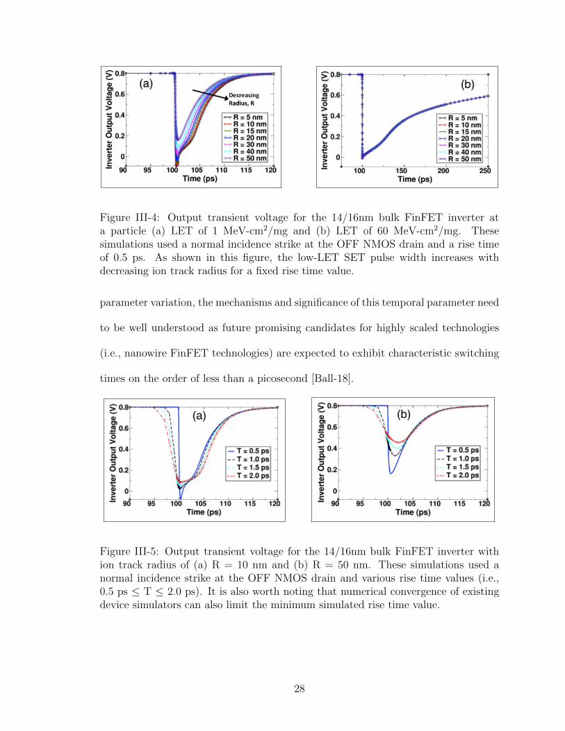
Figure III-4: Output transient voltage for the 14/16nm bulk FinFET inverter ata particle (a) LET of 1 MeV-cm2/mg and (b) LET of 60 MeV-cm2/mg. Thesesimulations used a normal incidence strike at the OFF NMOS drain and a rise timeof 0.5 ps. As shown in this figure, the low-LET SET pulse width increases withdecreasing ion track radius for a fixed rise time value.
parameter variation, the mechanisms and significance of this temporal parameter need
to be well understood as future promising candidates for highly scaled technologies
(i.e., nanowire FinFET technologies) are expected to exhibit characteristic switching
times on the order of less than a picosecond [Ball-18].
Figure III-5: Output transient voltage for the 14/16nm bulk FinFET inverter withion track radius of (a) R = 10 nm and (b) R = 50 nm. These simulations used anormal incidence strike at the OFF NMOS drain and various rise time values (i.e.,0.5 ps ≤ T ≤ 2.0 ps). It is also worth noting that numerical convergence of existingdevice simulators can also limit the minimum simulated rise time value.
28
Evolution of Radiation-Generated Charge
One noteworthy observation for SE simulations of advanced technologies is the
time at which the SE-induced electron-hole pair (ehp) density using appropriate ion
track parameter values (e.g., R = 10 nm and T = 0.5 ps, based on small device size and
circuit switching characteristics of advanced technologies) matches with radiation-
generated ehp density using the traditional spatial SE parameter assumption (i.e., R
= 50 nm), as shown in Figure III-6. The generated ehp density profile is shown for
the onset of the ion hit (0 ps), 1 ps, and 5 ps after an ion hit at the OFF-NMOS body
of the 14/16nm bulk FinFET inverter cell. It is worth noting that the illustrative
notation of the SE onset ('0 ps') for the TCAD simulations does not precisely equal
'zero time′ for the ion event. For these simulations, 'zero time′ refers to a start
time immediately following the thermalization of the initially generated hot carriers
(approximately less than one picosecond after the ion strike). The red curves and blue
curves of Figure III-6 represent the simulated SE ehp densities using the ion Track
1 (with a rise time of 0.5 ps and a small track radius of 10 nm) and the ion Track 2
(with a small rise time of 2 ps and a large track radius of 50 nm), respectively.
Simulation results in Figure III-6 show that the initial charge core (related to
SE-induced ehp density) is very dense and localized in the very small active volume
of the FinFET device (as indicated by the double-ended arrow of the FinFET fin
width). In addition, the onset peak ehp density of Track 1 matches that of Track 2
at around 5 ps after the ion strike, as depicted in Figure III-6. However, at times
less than 5 ps, the peak ehp density of Track 1 and Track 2 are very different. If
the impacted circuit responds fast enough to collect and integrate this charge on this
time scale, then the induced nodal currents for the two track examples would be
29
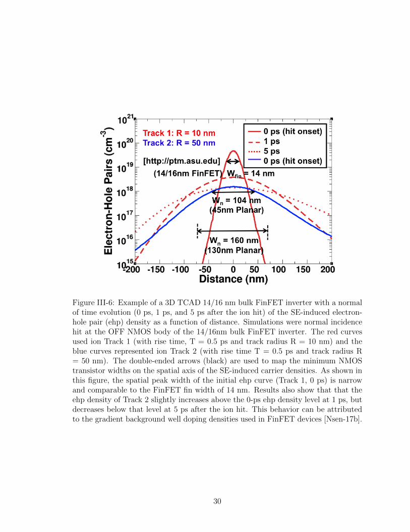
Figure III-6: Example of a 3D TCAD 14/16 nm bulk FinFET inverter with a normalof time evolution (0 ps, 1 ps, and 5 ps after the ion hit) of the SE-induced electron-hole pair (ehp) density as a function of distance. Simulations were normal incidencehit at the OFF NMOS body of the 14/16nm bulk FinFET inverter. The red curvesused ion Track 1 (with rise time, T = 0.5 ps and track radius R = 10 nm) and theblue curves represented ion Track 2 (with rise time T = 0.5 ps and track radius R= 50 nm). The double-ended arrows (black) are used to map the minimum NMOStransistor widths on the spatial axis of the SE-induced carrier densities. As shown inthis figure, the spatial peak width of the initial ehp curve (Track 1, 0 ps) is narrowand comparable to the FinFET fin width of 14 nm. Results also show that that theehp density of Track 2 slightly increases above the 0-ps ehp density level at 1 ps, butdecreases below that level at 5 ps after the ion hit. This behavior can be attributedto the gradient background well doping densities used in FinFET devices [Nsen-17b].
30
very different. As a result, latch-type circuit response perhaps even upset versus no
upset – in each case would be distinct. This observation is very important for SE
simulations of advanced FinFET technology nodes, which are characterized by small
sensitive volumes and fast switching characteristic times (i.e., one picosecond for a
14/16nm FinFET inverters). These simulation results also demonstrate that for sub-
22nm devices, the relevant region of influence - the volume where energy deposition
impacts a node is much smaller than the spatial extent of an ion interaction.
Impact of Spatial Track Parameter on 14nm SOI FinFET SRAM Upset Response
3D TCAD simulation results of the 14nm SOI FinFET SRAM show that the
appropriate temporal track parameter (rise time, T) for FinFET technologies is less
than two picoseconds and the spatial track parameter (radius, R) is ∼ 5 - 10 nm, as
shown in Figure III-7. For example, SE simulations using an ion track rise time, T of
0.5 ps with a radius, R of 5 - 10 nm result in the critical SEU current necessary to
upset the 14nm SOI FinFET SRAM cell at a particle LET of 1 MeV-cm2/mg. This
SEU current for R = 5 nm is more than twice than that of R = 80 nm for the same
particle LET of 1 MeV-cm2/mg, as shown in Figure III-7.
The use of a wide track radius of 80 nm and a rise time of 0.5 ps also overestimates
the radiation hardness of the 14nm SOI SRAM cell since the SEU current model
upsets the SRAM cell at a very high critical LET (LETcrit) of ∼ 17 MeV-cm2/mg (or
at a very high critical charge, Qcrit of ∼ 4.25 fC), as shown in Figure 8. However, with
appropriate SEU current model parameter values (i.e., the same T value of 0.5 ps,
but with any R in the range of 5–10 nm) that are consistent with the switching time
31
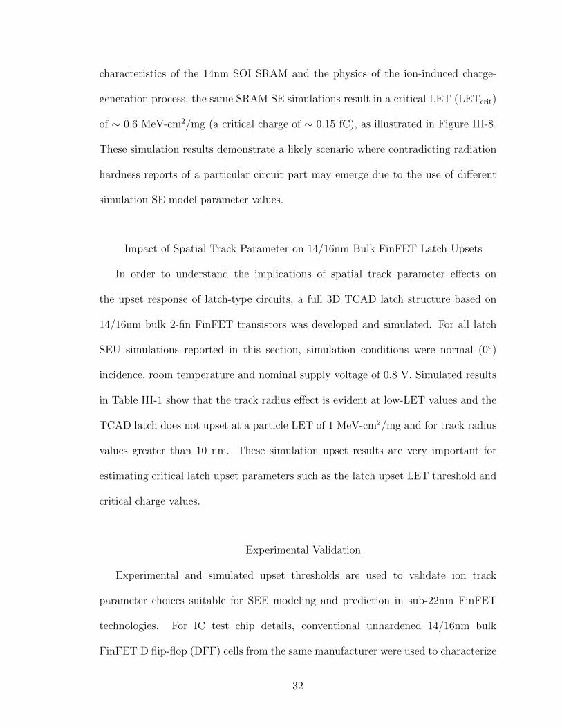
characteristics of the 14nm SOI SRAM and the physics of the ion-induced charge-
generation process, the same SRAM SE simulations result in a critical LET (LETcrit)
of ∼ 0.6 MeV-cm2/mg (a critical charge of ∼ 0.15 fC), as illustrated in Figure III-8.
These simulation results demonstrate a likely scenario where contradicting radiation
hardness reports of a particular circuit part may emerge due to the use of different
simulation SE model parameter values.
Impact of Spatial Track Parameter on 14/16nm Bulk FinFET Latch Upsets
In order to understand the implications of spatial track parameter effects on
the upset response of latch-type circuits, a full 3D TCAD latch structure based on
14/16nm bulk 2-fin FinFET transistors was developed and simulated. For all latch
SEU simulations reported in this section, simulation conditions were normal (0◦)
incidence, room temperature and nominal supply voltage of 0.8 V. Simulated results
in Table III-1 show that the track radius effect is evident at low-LET values and the
TCAD latch does not upset at a particle LET of 1 MeV-cm2/mg and for track radius
values greater than 10 nm. These simulation upset results are very important for
estimating critical latch upset parameters such as the latch upset LET threshold and
critical charge values.
Experimental Validation
Experimental and simulated upset thresholds are used to validate ion track
parameter choices suitable for SEE modeling and prediction in sub-22nm FinFET
technologies. For IC test chip details, conventional unhardened 14/16nm bulk
FinFET D flip-flop (DFF) cells from the same manufacturer were used to characterize
32
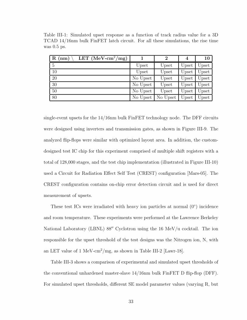
Table III-1: Simulated upset response as a function of track radius value for a 3DTCAD 14/16nm bulk FinFET latch circuit. For all these simulations, the rise timewas 0.5 ps.
R (nm) \ LET (MeV-cm2/mg) 1 2 4 10
5 Upset Upset Upset Upset
10 Upset Upset Upset Upset
20 No Upset Upset Upset Upset
30 No Upset Upset Upset Upset
50 No Upset Upset Upset Upset
80 No Upset No Upset Upset Upset
single-event upsets for the 14/16nm bulk FinFET technology node. The DFF circuits
were designed using inverters and transmission gates, as shown in Figure III-9. The
analyzed flip-flops were similar with optimized layout area. In addition, the custom-
designed test IC chip for this experiment comprised of multiple shift registers with a
total of 128,000 stages, and the test chip implementation (illustrated in Figure III-10)
used a Circuit for Radiation Effect Self Test (CREST) configuration [Mars-05]. The
CREST configuration contains on-chip error detection circuit and is used for direct
measurement of upsets.
These test ICs were irradiated with heavy ion particles at normal (0◦) incidence
and room temperature. These experiments were performed at the Lawrence Berkeley
National Laboratory (LBNL) 88′′ Cyclotron using the 16 MeV/u cocktail. The ion
responsible for the upset threshold of the test designs was the Nitrogen ion, N, with
an LET value of 1 MeV-cm2/mg, as shown in Table III-2 [Lawr-18].
Table III-3 shows a comparison of experimental and simulated upset thresholds of
the conventional unhardened master-slave 14/16nm bulk FinFET D flip-flop (DFF).
For simulated upset thresholds, different SE model parameter values (varying R, but
33

Table III-2: Ion beam details (16 MeV/u cocktail components [Lawr-18]) used forexperimental validation.
Ion Energy LET Rangefinal
(MeV) (MeV-cm2/mg (µm)14N+5 234 1 508
the same Gaussian rise time of 0.5 ps) were used. Results show that the use of a wide
ion track radius, R (i.e., the conventional 3D TCAD assumption of R = 50 nm for
single-event simulations) overestimates the simulated upset threshold (i.e., 3.4 MeV-
cm2/mg) compared to the experimental upset LET threshold of 1.16 MeV-cm2/mg,
as shown in Table III-3. However, the use of a small ion track radius (i.e., R ≤ 20
nm) resulted in upset LET thresholds that are approximately the same as that of
experimental data [Nsen-16].
Table III-3: Experimental versus simulated upset LET thresholds for 14/16nm bulkFinFET DFF (using a rise time of 0.5 ps for all simulations).
Type of results Upset LET threshold(MeV-cm2/mg)
Experimental data [Nsen-16] 1.16
Simulated w/R = 5 nm 1.10
Simulated w/R = 10 nm 1.16
Simulated w/R = 20 nm 1.40
Simulated w/R = 30 nm 3.10
Simulated w/R = 50 nm 3.40
Moreover, unlike simulated Qcrit based on a large R value (i.e., R = 80 nm), the
14nm SOI FinFET SRAM SE simulations using a small ion track radius of 5 nm
indicate a critical charge, Qcrit of 0.15 fC that is in a better agreement with historical
SRAM Qcrit scaling trends, as demonstrated in Figure III-11. These results show that
34
inaccurate choices of simulated SE ion track spatial and temporal parameter values
can yield misleading SE characterization information (for advanced circuits) that is
far different from experimental data.
Considerations for SE Simulations of Future Technology Nodes
3D TCAD simulations have generally assumed that the starting point of SE-
induced mechanisms (that are critical to the switching and performance of digital
circuits) occur after thermalization of the carriers (i.e., the carrier energies relax to
the values determined by the equilibrium distribution function). This thermalization
of initially generated carriers in a semiconductor device by a highly energetic ion is a
relatively fast process and only lasts for a very short time (on the order of less than one
picosecond) after the ion strike. So far, for technology nodes down to 14/16nm, the
judicious use of existing SE simulation models has been able to match experimentally
measured SE responses, indicating that the processes that occur on the thermalization
time scale are not of first-order significance. However, as semiconductor devices
continue to get smaller and achieve faster circuit switching speeds, the sensitivity
of simulation results to spatial and temporal parameters will be important and will
have to be accounted for (in simulation tools and SEE analyses) in order to accurately
calculate error rates of terrestrial and space electronic systems.
Conclusions
With technology scaling below 22nm, and circuit response times below 10 ps, the
spatial and temporal model parameter values assumed when simulating device- and
circuit-level single-event effects using 3D TCAD simulations show a significant impact
35

on the simulated SE results. Thorough SE sensitivity study cases using 14nm SOI
FinFET SRAM cells, 14/16nm bulk FinFET inverter, and 14/16nm bulk FinFET D
latch/flip-flop circuits showed that the use of a small ion track radius (R ≤ 20 nm)
and a short rise time (T < 2 ps) is necessary to produce simulation results that are
in agreement with historical critical charge scaling trends and measured upset LET
thresholds. For example, the use of a track radius, R, on the order of R ≥ 50 nm (a
historically used value) predicts an upset LET threshold of 17 MeV-cm2/mg (a critical
charge of over 4 fC), which would make the SRAM cell difficult to write electrically.
The use of R = 5 nm results in a predicted upset LET threshold of 0.6 MeV-cm2/mg
(∼ 0.15 fC) a value much more consistent with the expectation based on well-known
technology scaling trends. The suggested SE model parameter values are consistent
with the physics of ion-induced charge-generation processes, focusing on the dense
charge tracks that are created at early times (on the order of < 1 ps). The dimension
of the dense tracks are on the order of key dimensions of the active devices (channel
lengths and fin widths), and the time frame is on the order of switching time of
advanced digital circuits. The findings of this work can be useful to device/circuit
designers and the radiation-induced effects community in general, for accurate error
rate calculations of bulk FinFET-based digital circuits used in terrestrial and space
applications.
36
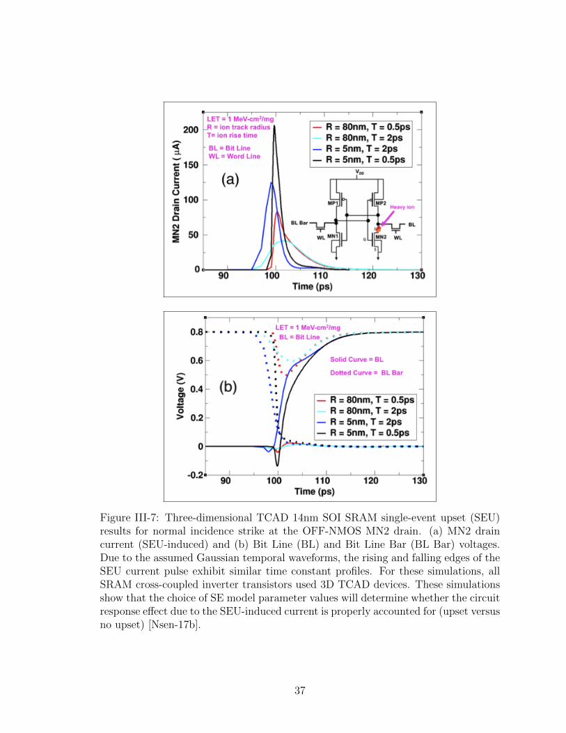
Figure III-7: Three-dimensional TCAD 14nm SOI SRAM single-event upset (SEU)results for normal incidence strike at the OFF-NMOS MN2 drain. (a) MN2 draincurrent (SEU-induced) and (b) Bit Line (BL) and Bit Line Bar (BL Bar) voltages.Due to the assumed Gaussian temporal waveforms, the rising and falling edges of theSEU current pulse exhibit similar time constant profiles. For these simulations, allSRAM cross-coupled inverter transistors used 3D TCAD devices. These simulationsshow that the choice of SE model parameter values will determine whether the circuitresponse effect due to the SEU-induced current is properly accounted for (upset versusno upset) [Nsen-17b].
37

Figure III-8: Simulated critical charge (Qcrit) and critical LET (LETcrit) as a functionof ion track radius for SEU characterization of the 14nm SOI FinFET SRAM.Simulations were performed using normal incidence hit at the OFF NMOS drainas shown by the inset SRAM circuit in Figure III-7 (a) [Nsen-17b].
Figure III-9: Example of a conventional edge-triggered transmission gate D flip-flop(TG DFF) implemented in a master-slave configuration. The upset of the TG DFFis due to the injected SET in the master stage latch.
38

Figure III-10: A schematic representation of the SEU test chip structure with thebasic concept of the CREST block level design used for evaluating flip-flop SEUresponse. The test chip consists of several shift register chains with on-chip errordetection circuit on the output and a common input for each chain [Mars-05].
Figure III-11: Comparison of simulated critical charge, Qcrit against historical scalingtrends of Qcrit as a function of feature size. As shown in this figure, the simulatedQcrit value for the 14nm SOI FinFET SRAM using ion track parameter values (i.e.,R = 5 nm and T = 0.5 ps) suitable for advanced (small and fast) digital circuitsproduces a better agreement with historical Qcrit scaling trends. Plot courtesy L.W.Massengill et al. [Mass-12].
39
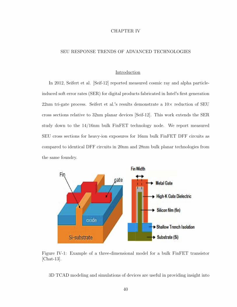
CHAPTER IV
SEU RESPONSE TRENDS OF ADVANCED TECHNOLOGIES
Introduction
In 2012, Seifert et al. [Seif-12] reported measured cosmic ray and alpha particle-
induced soft error rates (SER) for digital products fabricated in Intel's first generation
22nm tri-gate process. Seifert et al.'s results demonstrate a 10× reduction of SEU
cross sections relative to 32nm planar devices [Seif-12]. This work extends the SER
study down to the 14/16nm bulk FinFET technology node. We report measured
SEU cross sections for heavy-ion exposures for 16nm bulk FinFET DFF circuits as
compared to identical DFF circuits in 20nm and 28nm bulk planar technologies from
the same foundry.
Figure IV-1: Example of a three-dimensional model for a bulk FinFET transistor[Chat-13].
3D TCAD modeling and simulations of devices are useful in providing insight into
40
physical mechanisms and failure modes due to single-event effects [Akti-11, Chen-
12]. In this work, 3D TCAD simulations were used to investigate charge collection
mechanisms and SET pulse widths at the advanced nanoscale fabrication nodes
analyzed in this Chapter IV. Given the smaller size and higher drive current of the
16nm bulk FinFETs compared to planar nodes, it can be hypothesized that SET pulse
widths for the 16nm bulk FinFET for low LET particles will be relatively shorter
than those of their planar counterparts. For high LET particles, however, both bulk
FinFET and bulk planar advanced technology nodes are expected to exhibit similar
radiation-induced transients due to the increased substrate charge collection [El-Ma-
11b]. In addition, the effect of well debiasing on the p-FinFET could also be a
major factor, where the well/substrate junction plays an important role in the charge
collection mechanisms of bulk FinFETs.
Experiments
Test Circuit Description and Experimental Setup
Conventional DFFs at three different advanced technology nodes, but from the
same manufacturer, were designed using inverters and transmission gates as shown
in Figure IV-2. All the analyzed D flip-flops were similar with optimized layout area.
The flip-flop cells were used in a shift register. For 28nm and 20nm test ICs, the shift
register was 8K stages long. For the 16nm test IC, one shift register with a total of
128,000 stages was used.
These flip-flops were irradiated with heavy-ion particles at normal (0◦) incidence
and room temperature in order to investigate the SEU response. The test IC chips
41

Figure IV-2: Example of a conventional edge-triggered transmission gate DFF (TGDFF) implemented in a master-slave configuration. The upset of the TG DFF is dueto the injected SET in the master stage latch.
were operated at the nominal supply voltages (i.e., VDD of 900 mV for the 28nm
bulk planar technology node, 850 mV for the 20nm bulk planar technology node, and
800 mv for the 16nm bulk FinFET technology nodes). Experiments for the 16nm
bulk FinFET circuits were performed at the Lawrence Berkeley National Laboratory
(LBNL) 88′′ Cyclotron using the 16 MeV/u cocktail with seven different ions (N, Ne,
Si, Ar, Cu, Kr, and Xe) and a range of particle LETs of 1 to 49 MeV-cm2/mg, as
shown in Table IV-1 [Lawr-18]. The 20nm and 28nm bulk planar circuits were also
tested at the LBNL 88′′ Cyclotron using the 10 MeV/u cocktail beam with eight
different ions (B, O, Ne, Ar, V, Cu, Kr, and Xe) as indicated in Table IV-2. It is
worth noting that the effect of the ion energy difference on SEU cross sections was
not significant and did not affect the comparison presented in this work.
42
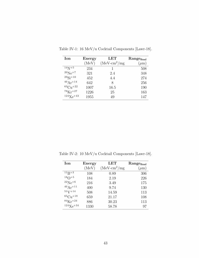
Table IV-1: 16 MeV/u Cocktail Components [Lawr-18].
Ion Energy LET Rangefinal
(MeV) (MeV-cm2/mg (µm)14N+5 234 1 50820Ne+7 321 2.4 34829Si+10 452 4.4 27440Ar+14 642 8 25663Cu+22 1007 16.5 19078Kr+27 1226 25 163124Xe+43 1955 49 147
Table IV-2: 10 MeV/u Cocktail Components [Lawr-18].
Ion Energy LET Rangefinal
(MeV) (MeV-cm2/mg (µm)11B+3 108 0.89 30618O+5 184 2.19 22622Ne+6 216 3.49 17540Ar+11 400 9.74 13051V+14 508 14.59 11365Cu+18 659 21.17 10884Kr+24 886 30.23 113124Xe+34 1330 58.78 97
43

Measured SEU Cross Section Trends
Experimental heavy-ion data for both 28/20nm bulk planar and 16nm bulk
FinFET flip-flops are reported. In all depicted data plots, error bars were calculated
using the standard error, and are smaller than the data symbols. Heavy-ion
experimental measurements are shown in Figure IV-3. These measurements show
that the SEU cross sections per FF decrease with technology scaling, as expected.
A similar trend of decreasing SEU cross sections with technology scaling has been
reported in [Gasp-13]. The improvement in SEU cross section between 28nm and
20nm was not significant. The 20nm planar DFF exhibited cross section values
approximately 2× lower than those of the 28nm planar DFFs across all LET values
as illustrated in Figure IV-3.
Figure IV-3: Experimental SEU response trend of 16nm bulk FinFET, 20nm bulkplanar, and 28nm bulk planar DFFs. Error bars are smaller than the data points,except for the error bar of the FinFET SEU cross section at the lowest LET particle.The inset figure is an example of the circuit schematic for the standard transmissiongate DFF (TG DFF). The ′φ′ parameter is the clock signal and the ′φb
′ is the invertedclock signal [Nara-15].
44

The improvement between the 20nm planar technology node and the 16nm
FinFET node was more pronounced, especially for low LET particles. For particles
with very low LET, around 1 MeV-cm2/mg, the improvement in SEU cross section is
orders of magnitude better for 16nm FinFET node over 20nm planar node, while only
2× SEU improvement is observed between 28nm planar and 20nm planar technology
nodes. The observed improvement of the 16nm bulk FinFET over planar technologies
can be explained by the highly scaled feature sizes of the 16nm FinFET technology
node. Only direct hits to the drain node by low LET particles can cause an upset
in 16nm FinFET technology node. These results clearly demonstrate the superior
performance of FinFET technology node for low-LET particles. For the terrestrial
environment where low-LET particles dominate the soft error rates (SER), such an
improvement will significantly lower the overall SE error rates for FinFET circuits.
However, for the particles with high LET values, above 20 MeV-cm2/mg, the
advantage of FinFET technology disappears. Between 28nm planar node and 20nm
planar node, the difference in cross section for high LET particles is not significant.
Unexpectedly, the same is seen between the 20nm planar node and 16nm FinFET
technology node.
These results clearly demonstrate the advantage of fin structure against charge
collection after an ion hit. The thin drain region and the narrow connection to the
substrate reduce the total volume that is sensitive to an ion hit as shown in Figure
IV-4. For low LET particles, only those particles that directly hit a drain region
can cause an upset. The probability of a direct hit on a drain region is much lower
for FinFET than that for a planar transistor drain region, resulting in significant
reduction in cross section for low LET particles.
45
For high LET particles, there is significant charge collection from the bulk/sub-
strate region [Tam-15]. As a result, the heavy-ion cross section of the 16nm DFF for a
high LET particle is very similar to those for 20nm and 28nm DFFs. This observation
is important for the potential application of FinFET technologies in space deployment.
3D TCAD Simulations
3D TCAD SE simulations were performed for all three analyzed technologies. In
all TCAD analyses, Synopsys Sentaurus tools [Syno-12] were used in the modeling
and simulations of SEE. The dimensions and transistor feature sizes of the simulated
devices were informed based on data from commercial process design kits (PDKs),
the International Technology Roadmap for Semiconductors (ITRS) [ITRS-15], and the
Predictive Technology Model (PTM) from Arizona State University (ASU) [Ariz-18].
The ASU PTM provides predictive model files for future transistor and interconnect
technologies that are compatible with industry standard circuit simulator, such as
SPICE, and are scalable with a wide range of process variations.
3D TCAD simulations of the struck inverter (shown Figure IV-5 and Figure IV-6)
were used to explore charge collection mechanisms and SET pulse widths. Although
the entire DFF was not simulated due to the unavailability of the 16nm bulk FinFET
PDK, 3D TCAD devices developed for this study are capable of yielding accurate
results for predictive analysis. The simulated inverter shown in Figure IV-5 and
Figure IV-6 constitutes the basic building block of the tested TG DFF circuit and is
part of the sensitive feedback loop of the same flip-flop as shown in Figure IV-2.
The simulated 16nm bulk n-FinFET and p-FinFET devices had an effective
channel length LG of 16nm as depicted in Figure IV-6. Moreover, both 16nm bulk
46
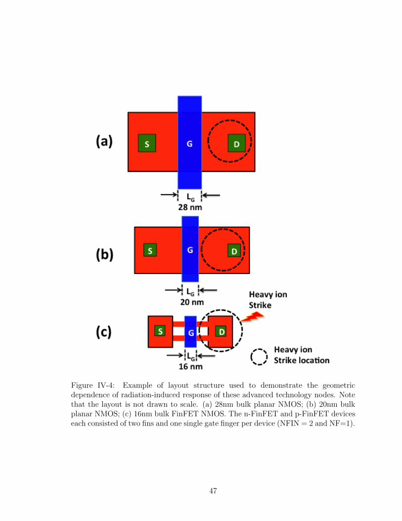
Figure IV-4: Example of layout structure used to demonstrate the geometricdependence of radiation-induced response of these advanced technology nodes. Notethat the layout is not drawn to scale. (a) 28nm bulk planar NMOS; (b) 20nm bulkplanar NMOS; (c) 16nm bulk FinFET NMOS. The n-FinFET and p-FinFET deviceseach consisted of two fins and one single gate finger per device (NFIN = 2 and NF=1).
47
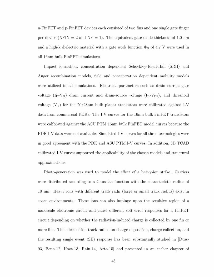
n-FinFET and p-FinFET devices each consisted of two fins and one single gate finger
per device (NFIN = 2 and NF = 1). The equivalent gate oxide thickness of 1.0 nm
and a high-k dielectric material with a gate work function ΦG of 4.7 V were used in
all 16nm bulk FinFET simulations.
Impact ionization, concentration dependent Schockley-Read-Hall (SRH) and
Auger recombination models, field and concentration dependent mobility models
were utilized in all simulations. Electrical parameters such as drain current-gate
voltage (ID-VG) drain current and drain-source voltage (ID-VDS), and threshold
voltage (VT) for the 20/28nm bulk planar transistors were calibrated against I-V
data from commercial PDKs. The I-V curves for the 16nm bulk FinFET transistors
were calibrated against the ASU PTM 16nm bulk FinFET model curves because the
PDK I-V data were not available. Simulated I-V curves for all three technologies were
in good agreement with the PDK and ASU PTM I-V curves. In addition, 3D TCAD
calibrated I-V curves supported the applicability of the chosen models and structural
approximations.
Photo-generation was used to model the effect of a heavy-ion strike. Carriers
were distributed according to a Gaussian function with the characteristic radius of
10 nm. Heavy ions with different track radii (large or small track radius) exist in
space environments. These ions can also impinge upon the sensitive region of a
nanoscale electronic circuit and cause different soft error responses for a FinFET
circuit depending on whether the radiation-induced charge is collected by one fin or
more fins. The effect of ion track radius on charge deposition, charge collection, and
the resulting single event (SE) response has been substantially studied in [Duss-
93, Benn-12, Hoot-13, Rain-14, Arto-15] and presented in an earlier chapter of
48

this dissertation (i.e., Chapter III). The choice of the track radius has become
an important step in the modeling process of single event hits in current nanoscale
technologies because the radial energy deposition distribution is of the same order as
the size of the struck device [Rain-14, Arto-15].
Moreover, photo-carrier generation was modeled only in the drain region of a p-
type or n-type Metal-Oxide-Semiconductor Field-Effect Transistor (MOSFET). For
all simulated heavy-ion strikes presented in this Chapter IV, only normal incidence
strikes were carried out and the hit transistor was in the OFF-state condition as this
is the single-event sensitive state of the device.
Figure IV-5 shows an example of a 3D TCAD simulated 20nm bulk planar inverter
used in this study. The 3D TCAD simulation approach for the 28nm bulk planar
technology node is analogous to that of the 20nm bulk planar inverter. Similarly,
Figure IV-6 depicts a 3D TCAD model for the simulated 16nm two-fin bulk FinFET
inverter used in this chapter. In all reported inverter simulations, both the n-channel
and p-channel transistors were full 3D TCAD transistors.
3D TCAD Simulation Results
To investigate charge collection mechanisms and SET pulse width trends for the
16nm bulk FinFET compared to SETs in 20/28nm bulk planar technologies, 3D
TCAD simulations were conducted and simulation results are discussed in this section.
Figure IV-7 shows 3D TCAD heavy-ion SET pulse widths as a function of LET value
for the 16nm bulk FinFET and 20/28nm planar technology nodes. The 16nm bulk
FinFET resulted in shorter SET pulse widths as opposed to longer SET pulse widths
for the 20/28nm planar technologies when heavy-ion particle LET was varied from 1
49
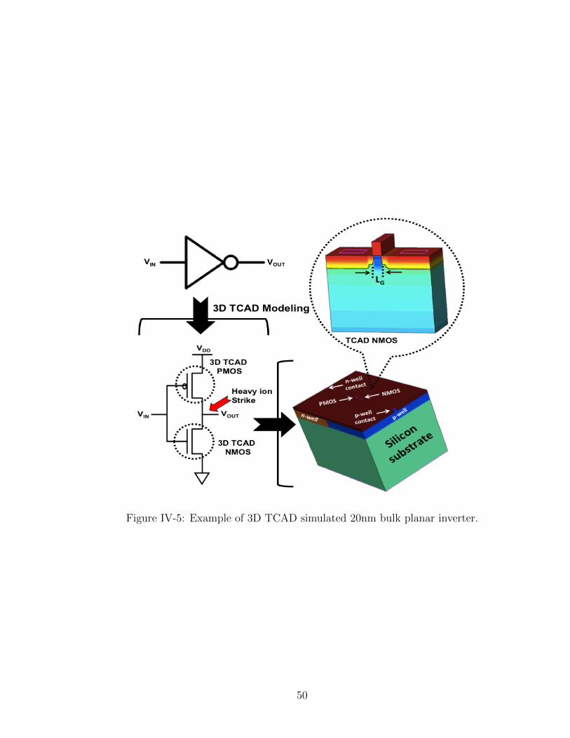
Figure IV-5: Example of 3D TCAD simulated 20nm bulk planar inverter.
50
Figure IV-6: Example of 3D TCAD 16nm bulk FinFET 2-fin NMOS/PMOStransistors wired in 3D TCAD inverter configuration. LG is the effective channellength of the transistor. Heavy-ion strikes at a normal incidence were carried out onthe drain of the OFF-state n-FinFET transistor.
51
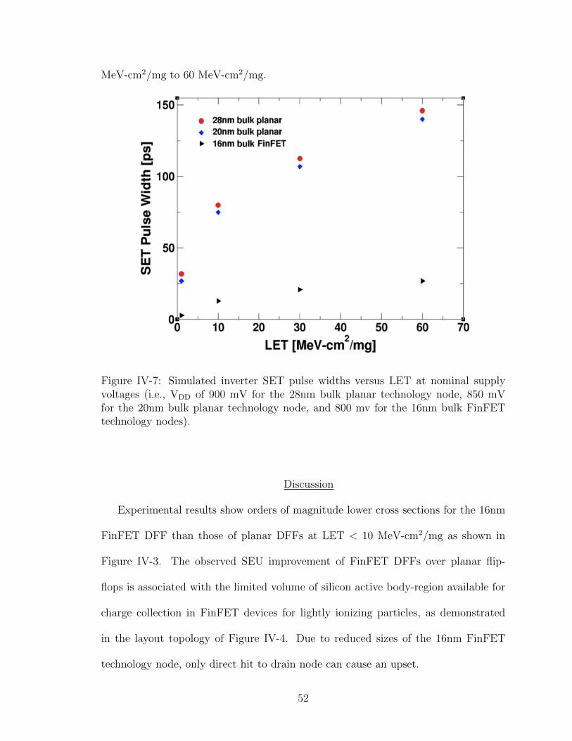
MeV-cm2/mg to 60 MeV-cm2/mg.
Figure IV-7: Simulated inverter SET pulse widths versus LET at nominal supplyvoltages (i.e., VDD of 900 mV for the 28nm bulk planar technology node, 850 mVfor the 20nm bulk planar technology node, and 800 mv for the 16nm bulk FinFETtechnology nodes).
Discussion
Experimental results show orders of magnitude lower cross sections for the 16nm
FinFET DFF than those of planar DFFs at LET < 10 MeV-cm2/mg as shown in
Figure IV-3. The observed SEU improvement of FinFET DFFs over planar flip-
flops is associated with the limited volume of silicon active body-region available for
charge collection in FinFET devices for lightly ionizing particles, as demonstrated
in the layout topology of Figure IV-4. Due to reduced sizes of the 16nm FinFET
technology node, only direct hit to drain node can cause an upset.
52
Simulated SET pulse widths for the 16nm bulk FinFET and 20/28nm bulk
planar technologies increase with LET value for nominal supply voltages of 900
mV as shown Figure IV-7. The 16nm bulk FinFET technology has shorter SET
pulse widths (3 ps – 27 ps) compared to longer SET pulse widths for the 20/28nm
planar technologies which range from 27 ps to 146 ps when the particle LET was
varied from 1 MeV-cm2/mg to 60 MeV-cm2/mg. Such an observation confirms the
improved SET response for the 16nm bulk FinFET, mostly below the threshold LET.
However, FinFET SET improvement vanishes for LET ≥ 10 MeV-cm2/mg because
the enhanced substrate charge collection at high-LET values.
Conclusions
This chapter presents a comparison of SEU response trends among 16nm bulk
FinFET, 20nm bulk planar, and 28nm bulk planar D flip-flops. Results show that
SEU cross sections do not reduce significantly with scaling for high-LET values. SEU
cross sections for the 16nm bulk FinFET flip-flops at a particle LET ≥ 10 MeV-
cm2/mg show only a 2× improvement compared to 20/28nm planar technologies. The
relatively small difference between FinFET SEU cross sections and those of planar
technology nodes for high LET values presents a radiation-induced SEE concern for
bulk FinFET circuits used in space and defense digital systems. In light of these
observations, it is recommended that radiation-hardening techniques be taken into
consideration for bulk FinFET-based circuits used in space and defense applications.
However, experimental data show orders of magnitude lower cross sections for the
16nm bulk FinFET D flip-flops than those of bulk planar D flip-flops at LET < 10
53
MeV-cm2/mg. For example, the SEU cross section for the 16nm bulk FinFET D flip-
flops is two orders of magnitude lower than that of 20nm bulk planar D flip-flops at
a particle LET of 1 MeV-cm2/mg. 3D TCAD simulations of the 16nm bulk FinFET
inverter also showed shorter SET pulse widths and lower collected charge compared
to SETs of 20/28nm planar inverters for LET below 10 MeV-cm2/mg. The observed
single-event improvement for low-LET particles is related to the threshold LET and
the relatively smaller hit drain area for the 16nm bulk FinFET technology node.
This observation is important for designers of modern electronic circuits intended to
perform in terrestrial environment where low LET particles dominate the single-event
error rates. Such an improvement will significantly lower the overall single-event error
rates for bulk FinFET designs.
Moreover, the insights of this work suggest that circuits exhibiting a low-LET
threshold (i.e., bulk FinFET circuits) are possibly sensitive to direct ionization
from singly-charged particles such as muons and protons. Recent studies of muon-
induced effects in bulk FinFET SRAM memory cells [Seif-15a, Infa-17] show that
the introduction of 3D tri-gate transistors reduced the susceptibility to muons by
approximately two orders of magnitude relative to the SEU cross section response
of a 32nm planar design [Seif-15a]. However, a thorough characterization of the
sensitivity of bulk FinFET logic devices (e.g., flip-flops, latches, and register files)
to protons is also recommended because of the abundance of these particles in both
terrestrial and space radiation environments.
54
CHAPTER V
ANALYSIS OF BULK FINFET STRUCTURAL EFFECTS ON SINGLE-EVENT
CROSS SECTIONS
Introduction
For a given storage cell design, the area over which critical charge (or more)
is collected at a circuit node is defined as the sensitive area for that node [Mavi-
07, Mass-93, Baum-05a, Baum-05b]. Charge collection processes and the resulting
sensitive area for individual transistors are integral to SEE modeling and predictive
analysis for advanced digital circuits.
A depiction of planar transistor structure versus FinFET structure is shown in
Figure V-1. Measured FF SEU cross-section data comparing similar FF cells at 28nm
bulk planar, 20nm bulk planar, and 16nm bulk FinFET technologies were presented
in Figure IV-3 (i.e., Chapter IV). The supporting simulation analyses in Chapter IV
demonstrated that the trends of the simulated SET pulse widths as function of particle
LET were consistent with the observed measured SE cross section data. However,
the analysis in Chapter IV did not produce a more quantitative agreement with
the measured FF SEU cross section data, and the key question of upset criteria to
bridge transistor-level SE response to circuit-level SE cross-section values remained.
For example, what is the proper integration time of the collected charge? Is the full
width at half maximum (FWHM) SET pulse width the appropriate upset criteria for
advanced (small and fast) digital circuits?
55
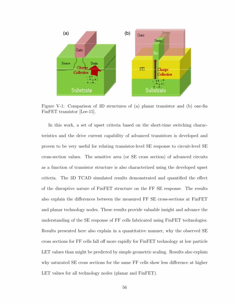
Figure V-1: Comparison of 3D structures of (a) planar transistor and (b) one-finFinFET transistor [Lee-15].
In this work, a set of upset criteria based on the short-time switching charac-
teristics and the drive current capability of advanced transistors is developed and
proven to be very useful for relating transistor-level SE response to circuit-level SE
cross-section values. The sensitive area (or SE cross section) of advanced circuits
as a function of transistor structure is also characterized using the developed upset
criteria. The 3D TCAD simulated results demonstrated and quantified the effect
of the disruptive nature of FinFET structure on the FF SE response. The results
also explain the differences between the measured FF SE cross-sections at FinFET
and planar technology nodes. These results provide valuable insight and advance the
understanding of the SE response of FF cells fabricated using FinFET technologies.
Results presented here also explain in a quantitative manner, why the observed SE
cross sections for FF cells fall off more rapidly for FinFET technology at low particle
LET values than might be predicted by simple geometric scaling. Results also explain
why saturated SE cross sections for the same FF cells show less difference at higher
LET values for all technology nodes (planar and FinFET).
56
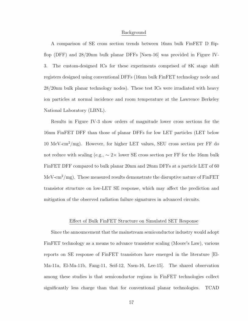
Background
A comparison of SE cross section trends between 16nm bulk FinFET D flip-
flop (DFF) and 28/20nm bulk planar DFFs [Nsen-16] was provided in Figure IV-
3. The custom-designed ICs for these experiments comprised of 8K stage shift
registers designed using conventional DFFs (16nm bulk FinFET technology node and
28/20nm bulk planar technology nodes). These test ICs were irradiated with heavy
ion particles at normal incidence and room temperature at the Lawrence Berkeley
National Laboratory (LBNL).
Results in Figure IV-3 show orders of magnitude lower cross sections for the
16nm FinFET DFF than those of planar DFFs for low LET particles (LET below
10 MeV-cm2/mg). However, for higher LET values, SEU cross section per FF do
not reduce with scaling (e.g., ∼ 2× lower SE cross section per FF for the 16nm bulk
FinFET DFF compared to bulk planar 20nm and 28nm DFFs at a particle LET of 60
MeV-cm2/mg). These measured results demonstrate the disruptive nature of FinFET
transistor structure on low-LET SE response, which may affect the prediction and
mitigation of the observed radiation failure signatures in advanced circuits.
Effect of Bulk FinFET Structure on Simulated SET Response
Since the announcement that the mainstream semiconductor industry would adopt
FinFET technology as a means to advance transistor scaling (Moore's Law), various
reports on SE response of FinFET transistors have emerged in the literature [El-
Ma-11a, El-Ma-11b, Fang-11, Seif-12, Nsen-16, Lee-15]. The shared observation
among these studies is that semiconductor regions in FinFET technologies collect
significantly less charge than that for conventional planar technologies. TCAD
57
simulations are used to indicate that the charge collection for semiconductor regions
in FinFET technologies is approximately reduced by 70% compared to that of planar
technologies [Fang-11]. Others investigated charge collection for FinFET technology
using laser and heavy ion irradiation tests, and demonstrated that the FinFET
sensitive area is mostly dominated by the drain diffusion area [El-Ma-11a, El-Ma-
11b].
It seems clear from these prior works that the reduced FinFET charge collection
efficiency can be explained by the FinFET transistor structure. This work also reveals
that the fin body area is the most sensitive region for SEE and the SE vulnerability
diminishes quickly as the ion particle strike location moves outside the active fin
region. As a result, a thorough analysis of the SE response due to the FinFET
transistor structural effect on charge collection processes is necessary.
Figure V-2 and Figure V-3 show a comparison of the SET response of an inverter
cell for 16nm bulk FinFET and 28nm bulk planar technologies using 3D TCAD
simulations for a normally incident particle. For low-LET particle strike (i.e., LET
of 1 MeV-cm2/mg), the SET response of the bulk FinFET inverter has a very strong
dependence on the ion strike location as shown in Figure V-2 (a). Results show that a
direct ion strike at the fin produces an observable single-event transient while an ion
strike between two fins results in a very small voltage perturbation. Unlike FinFET
technologies, the SE response of planar inverter shows little or no dependence on
strike location for low LET particles. For example, the ion strikes within the drain
region or in the vicinity of the drain region for the 28nm bulk planar MOSFET result
in the same SET response for a particle with LET of 1 MeV-cm2/mg. These effects
are attributable to the enhanced substrate charge collection of planar transistors
58
[Fang-11].
For strikes by particles with high-LET values, the FinFET SE response depen-
dence on the strike location diminishes due to the enhanced substrate (diffusion)
charge collection [Fang-11, El-Ma-11a]. Consequently, both direct hit at the fin and
hit between two fins result in the same SET response for particles with high-LET
values (i.e., LET of 60 MeV-cm2/mg), as shown in Figure V-3 (a).
The 28nm planar inverter also shows similar response to strikes by a high-LET
particle for all strike locations, as shown in Figure V-3 (b). These results provide
valuable insight and advance the understanding of SE response for FinFET technology
across a wide range of particle LET values. Results presented here also explain why
the observed SE cross sections of FinFET FF circuits decrease more quickly at low-
LET values than might be predicted by simple geometric scaling. These results also
illustrate why the saturated (or high-LET) SE cross sections of the same FF circuits
are consistent with simple area scaling across planar and FinFET technologies.
Simulation Setup and Analyses
Circuit-level simulations (using Cadence tool suite [Cade-18] and the SEE bias-
dependent model [Kaup-09]) and 3D TCAD simulations (using Synopsys Sentaurus
TCAD tools [Syno-12]) were performed for SE characterization and comparison of
16nm bulk FinFET technology node and 28/20nm bulk planar 28/20nm technology
nodes. The analyzed circuits consist of full 3D TCAD inverter structure and
conventional unhardened DFFs. Device drain current – gate voltage (ID–VG) curves
for both bulk planar transistors and bulk FinFET transistors were calibrated against
the I–V data from commercial PDKs and the Arizona State University Predictive
59
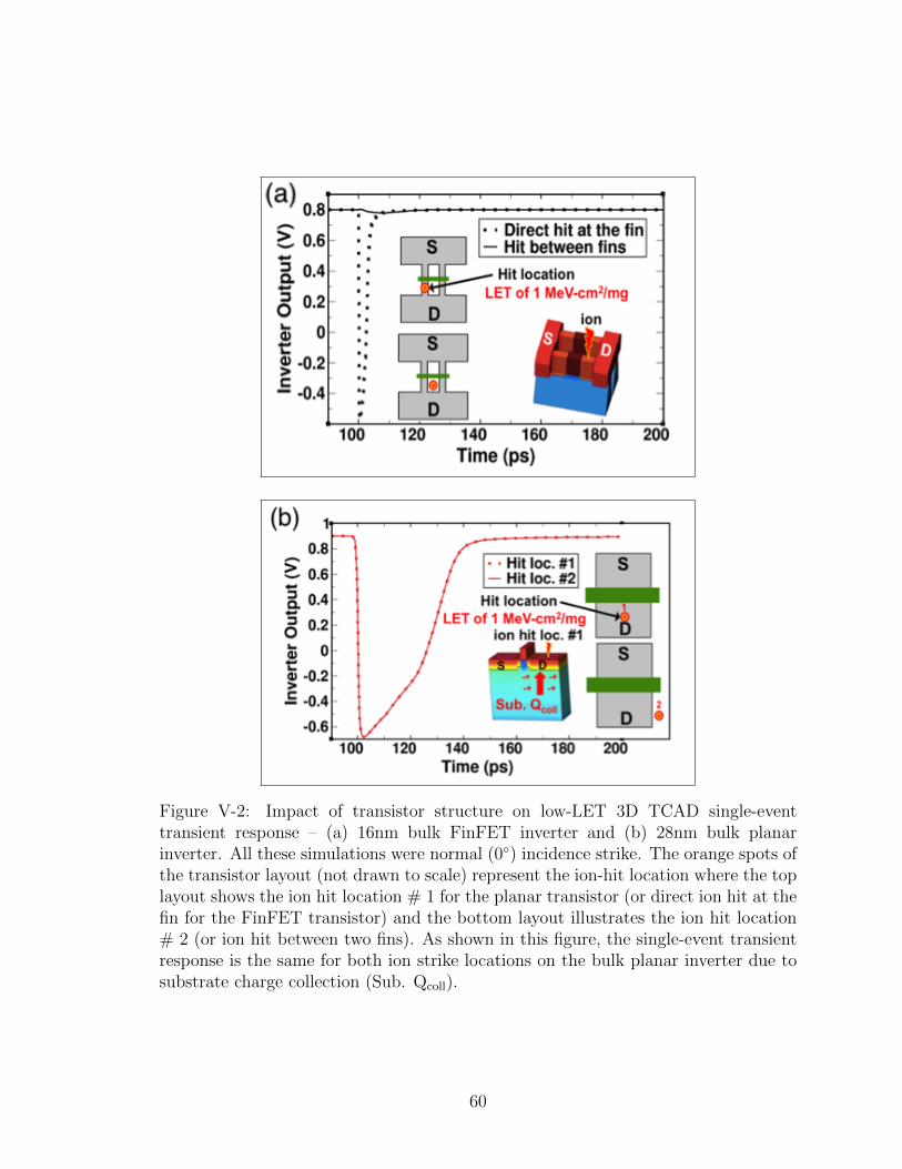
Figure V-2: Impact of transistor structure on low-LET 3D TCAD single-eventtransient response – (a) 16nm bulk FinFET inverter and (b) 28nm bulk planarinverter. All these simulations were normal (0◦) incidence strike. The orange spots ofthe transistor layout (not drawn to scale) represent the ion-hit location where the toplayout shows the ion hit location # 1 for the planar transistor (or direct ion hit at thefin for the FinFET transistor) and the bottom layout illustrates the ion hit location# 2 (or ion hit between two fins). As shown in this figure, the single-event transientresponse is the same for both ion strike locations on the bulk planar inverter due tosubstrate charge collection (Sub. Qcoll).
60

Figure V-3: Impact of transistor structure on high-LET 3D TCAD single-eventtransient response (a) 16nm bulk FinFET inverter and (b) 28nm bulk planar inverter.All these simulations were normal (0◦) incidence strike. The orange spots of thetransistor layout (not drawn to scale) represent the ion-hit location where the toplayout shows the ion hit location # 1 for the planar transistor (or direct ion hit at thefin for the FinFET transistor) and the bottom layout illustrates the ion hit location# 2 (or ion hit between two fins). It is worth noting that the high-LET single-eventtransient response on both ion strike location is the same for either bulk FinFETinverter or bulk planar inverter due to enhanced substrate charge collection (Sub.Qcoll).
61
Technology Model (PTM) [Ariz-18], respectively.
Moreover, the transistor width ratio (Wp/Wn) of 1.5 was used to obtain a matched
drive current for both planar PMOS and planar NMOS transistors. For the 16nm
bulk FinFET, the n-channel FinFET (n-FinFET) and p-channel FinFET (p-FinFET)
devices each consisted of two fins and one single gate finger per device (NFIN = 2 and
NF = 1). These n-FinFET and p-FinFET transistors were not drive-matched, but
were designed as minimum size transistors according to the design rules of the 16nm
bulk FinFET technology node. The 3D TCAD heavy ion model used in this work is
similar to the one discussed in [Nsen-16]. In addition, all of the reported simulations
here are for normal incidence and nominal supply voltages (VDD of 800 mV for the
16nm bulk FinFET technology node, 850 mV for the 20 nm bulk planar technology
node, and 900 mV for the 28 nm bulk planar technology node). The parameter
values of the charge track generated by a heavy ion model were a Gaussian charge
distribution with a track radius of 10 nm and a short rise time of 0.5 ps for all 3D
TCAD simulations. It should be noted that the appropriate choice of these spatial and
temporal model parameter values is important because they can significantly affect
the simulated results as discussed in Chapter III of this dissertation and [Nsen-17b].
Single-Event Upset Criteria
One of the fundamental logic building blocks in typical memory circuits (for
example, the TG DFF shown in Figure IV-2) is a CMOS inverter structure. The
switching behavior and the drive current capability of this basic logic gate (inverter)
play an important role in the SE response of digital memory circuits. Figure V-4
shows an example of the CMOS inverter voltage transfer characteristics (VTC) curve
62
for the 16nm bulk FinFET technology node. The VTC curve indicates the inverter
critical voltages, such as the input low voltage, VIL and the input high voltage, VIH.
The VIL voltage of an inverter is the maximum input value that generates a valid
high output voltage while the VIH voltage is the minimum input value that generates
a valid low output voltage. VIL and VIH voltages were estimated on the inverter
VTC curve where the slope of the inverter VTC curve is -1, as shown in Figure V-
4. These critical voltages were also verified using appropriate technology parameter
values (i.e., transistor transconductance value) by solving analytical expressions, as
stated in most digital circuit design texts [Uyem-02].
The voltage difference between VIH and VIL constitutes the transition width of
the CMOS inverter. An important parameter is the switching time (denoted here as
'ts′ of the CMOS inverter. The ts value is essentially the time difference of VIH and
VIL (i.e., ts = ∆Time (VIH, VIL)) in response to a step input. Figure V-5 shows an
example of the inverter waveforms with annotations of VIL, VIH, and ts values for the
16nm bulk FinFET inverter. The ts values for 20nm bulk planar inverter and 28nm
bulk planar inverter were extracted using SPICE simulation curves that are similar
to Figure V-5. In addition, Table V-1 shows the ts values for all three analyzed
technology nodes (i.e., 1 ps for the 16nm bulk FinFET node, 1.5 ps for the 20nm
bulk planar technology node, and 2 ps for the 28nm bulk planar technology node).
These results demonstrate that modern digital circuits are relatively very fast (where
the characteristic switching time, ts, is on the order of 1–2 ps) and their response
times are becoming comparable to the SE-induced charge deposition and collection
times [Nsen-17b]. The important impact of this temporal characteristic on simulated
SE results was discussed in Chapter III of this dissertation.
63
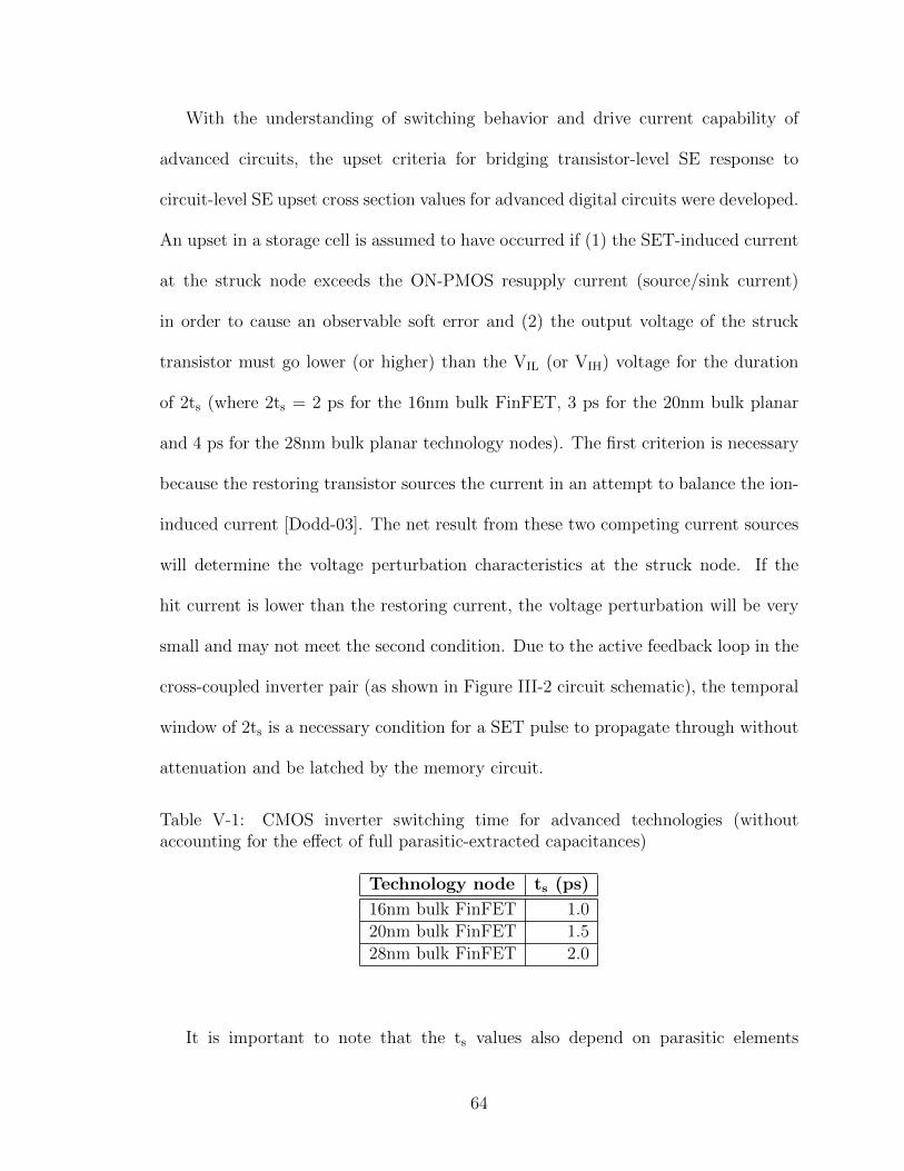
With the understanding of switching behavior and drive current capability of
advanced circuits, the upset criteria for bridging transistor-level SE response to
circuit-level SE upset cross section values for advanced digital circuits were developed.
An upset in a storage cell is assumed to have occurred if (1) the SET-induced current
at the struck node exceeds the ON-PMOS resupply current (source/sink current)
in order to cause an observable soft error and (2) the output voltage of the struck
transistor must go lower (or higher) than the VIL (or VIH) voltage for the duration
of 2ts (where 2ts = 2 ps for the 16nm bulk FinFET, 3 ps for the 20nm bulk planar
and 4 ps for the 28nm bulk planar technology nodes). The first criterion is necessary
because the restoring transistor sources the current in an attempt to balance the ion-
induced current [Dodd-03]. The net result from these two competing current sources
will determine the voltage perturbation characteristics at the struck node. If the
hit current is lower than the restoring current, the voltage perturbation will be very
small and may not meet the second condition. Due to the active feedback loop in the
cross-coupled inverter pair (as shown in Figure III-2 circuit schematic), the temporal
window of 2ts is a necessary condition for a SET pulse to propagate through without
attenuation and be latched by the memory circuit.
Table V-1: CMOS inverter switching time for advanced technologies (withoutaccounting for the effect of full parasitic-extracted capacitances)
Technology node ts (ps)
16nm bulk FinFET 1.0
20nm bulk FinFET 1.5
28nm bulk FinFET 2.0
It is important to note that the ts values also depend on parasitic elements
64
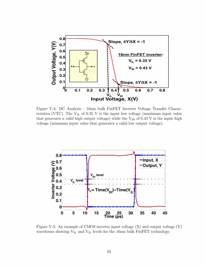
Figure V-4: DC Analysis – 16nm bulk FinFET Inverter Voltage Transfer Charac-teristics (VTC). The VIL of 0.35 V is the input low voltage (maximum input valuethat generates a valid high output voltage) while the VIH of 0.43 V is the input highvoltage (minimum input value that generates a valid low output voltage).
Figure V-5: An example of CMOS inverter input voltage (X) and output voltage (Y)waveforms showing VIL and VIL levels for the 16nm bulk FinFET technology.
65
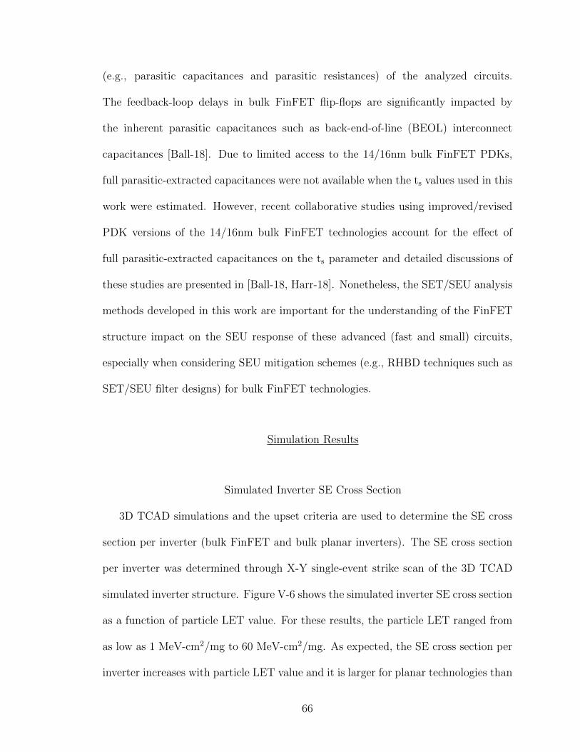
(e.g., parasitic capacitances and parasitic resistances) of the analyzed circuits.
The feedback-loop delays in bulk FinFET flip-flops are significantly impacted by
the inherent parasitic capacitances such as back-end-of-line (BEOL) interconnect
capacitances [Ball-18]. Due to limited access to the 14/16nm bulk FinFET PDKs,
full parasitic-extracted capacitances were not available when the ts values used in this
work were estimated. However, recent collaborative studies using improved/revised
PDK versions of the 14/16nm bulk FinFET technologies account for the effect of
full parasitic-extracted capacitances on the ts parameter and detailed discussions of
these studies are presented in [Ball-18, Harr-18]. Nonetheless, the SET/SEU analysis
methods developed in this work are important for the understanding of the FinFET
structure impact on the SEU response of these advanced (fast and small) circuits,
especially when considering SEU mitigation schemes (e.g., RHBD techniques such as
SET/SEU filter designs) for bulk FinFET technologies.
Simulation Results
Simulated Inverter SE Cross Section
3D TCAD simulations and the upset criteria are used to determine the SE cross
section per inverter (bulk FinFET and bulk planar inverters). The SE cross section
per inverter was determined through X-Y single-event strike scan of the 3D TCAD
simulated inverter structure. Figure V-6 shows the simulated inverter SE cross section
as a function of particle LET value. For these results, the particle LET ranged from
as low as 1 MeV-cm2/mg to 60 MeV-cm2/mg. As expected, the SE cross section per
inverter increases with particle LET value and it is larger for planar technologies than
66
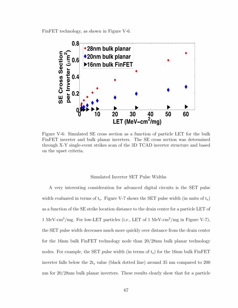
FinFET technology, as shown in Figure V-6.
Figure V-6: Simulated SE cross section as a function of particle LET for the bulkFinFET inverter and bulk planar inverters. The SE cross section was determinedthrough X-Y single-event strikes scan of the 3D TCAD inverter structure and basedon the upset criteria.
Simulated Inverter SET Pulse Widths
A very interesting consideration for advanced digital circuits is the SET pulse
width evaluated in terms of ts. Figure V-7 shows the SET pulse width (in units of ts)
as a function of the SE strike location distance to the drain center for a particle LET of
1 MeV-cm2/mg. For low-LET particles (i.e., LET of 1 MeV-cm2/mg in Figure V-7),
the SET pulse width decreases much more quickly over distance from the drain center
for the 16nm bulk FinFET technology node than 20/28nm bulk planar technology
nodes. For example, the SET pulse width (in terms of ts) for the 16nm bulk FinFET
inverter falls below the 2ts value (black dotted line) around 35 nm compared to 200
nm for 20/28nm bulk planar inverters. These results clearly show that for a particle
67
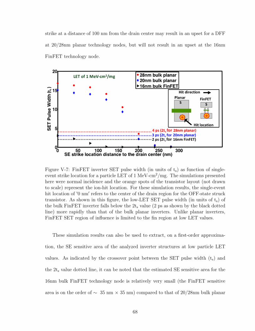
strike at a distance of 100 nm from the drain center may result in an upset for a DFF
at 20/28nm planar technology nodes, but will not result in an upset at the 16nm
FinFET technology node.
Figure V-7: FinFET inverter SET pulse width (in units of ts) as function of single-event strike location for a particle LET of 1 MeV-cm2/mg. The simulations presentedhere were normal incidence and the orange spots of the transistor layout (not drawnto scale) represent the ion-hit location. For these simulation results, the single-eventhit location of '0 nm′ refers to the center of the drain region for the OFF-state strucktransistor. As shown in this figure, the low-LET SET pulse width (in units of ts) ofthe bulk FinFET inverter falls below the 2ts value (2 ps as shown by the black dottedline) more rapidly than that of the bulk planar inverters. Unlike planar inverters,FinFET SET region of influence is limited to the fin region at low LET values.
These simulation results can also be used to extract, on a first-order approxima-
tion, the SE sensitive area of the analyzed inverter structures at low particle LET
values. As indicated by the crossover point between the SET pulse width (ts) and
the 2ts value dotted line, it can be noted that the estimated SE sensitive area for the
16nm bulk FinFET technology node is relatively very small (the FinFET sensitive
area is on the order of ∼ 35 nm × 35 nm) compared to that of 20/28nm bulk planar
68

technology nodes (which is on the order of ∼ 200 nm × 200 nm) for a particle LET
of 1 MeV-cm2/mg.
For high-LET particles, however, both planar and FinFET technologies exhibit
the same SE spatial sensitivity. For example, both planar and FinFET SET pulse
widths (ts) approach their respective 2ts values approximately at the same hit location
distance from the drain center (where a value of ∼ 240 nm is the estimated
intersection point of the SET pulse width curve and the 2ts dotted line), as shown
in Figure V-8. These high-LET simulation results show that the extracted inverter
SE sensitive area is on the order of ∼ 200 nm × 200 nm for all these advanced
technology nodes. The SE response behavior of planar and FinFET circuits at high
LET values is attributed to the increased charge collection (Qcoll) from the substrate.
The results shown here demonstrate why the observed SE cross sections for low-LET
particles for FinFET technology fall off more rapidly than might be predicted by
simple geometric scaling and why high-LET (saturated) FinFET single-event cross
sections are consistent with simple geometric area scaling (Moore's Law).
Calculated and Measured SE Cross Sections
The upset criteria and simulation results are used to relate transistor-level
SE response to circuit-level SEU cross section values. A comparative analysis of
calculated and measured SE cross sections per flip-flop for both FinFET and planar
technologies is also provided. For all of these simulations, the particle LET was
changed from as low as 1 MeV-cm2/mg to 60 MeV-cm2/mg and normal incidence
particle strikes were performed. The SE hit location was incrementally moved from
the center of the drain region ('0 nm′ location) to outside of the drain region of the
69
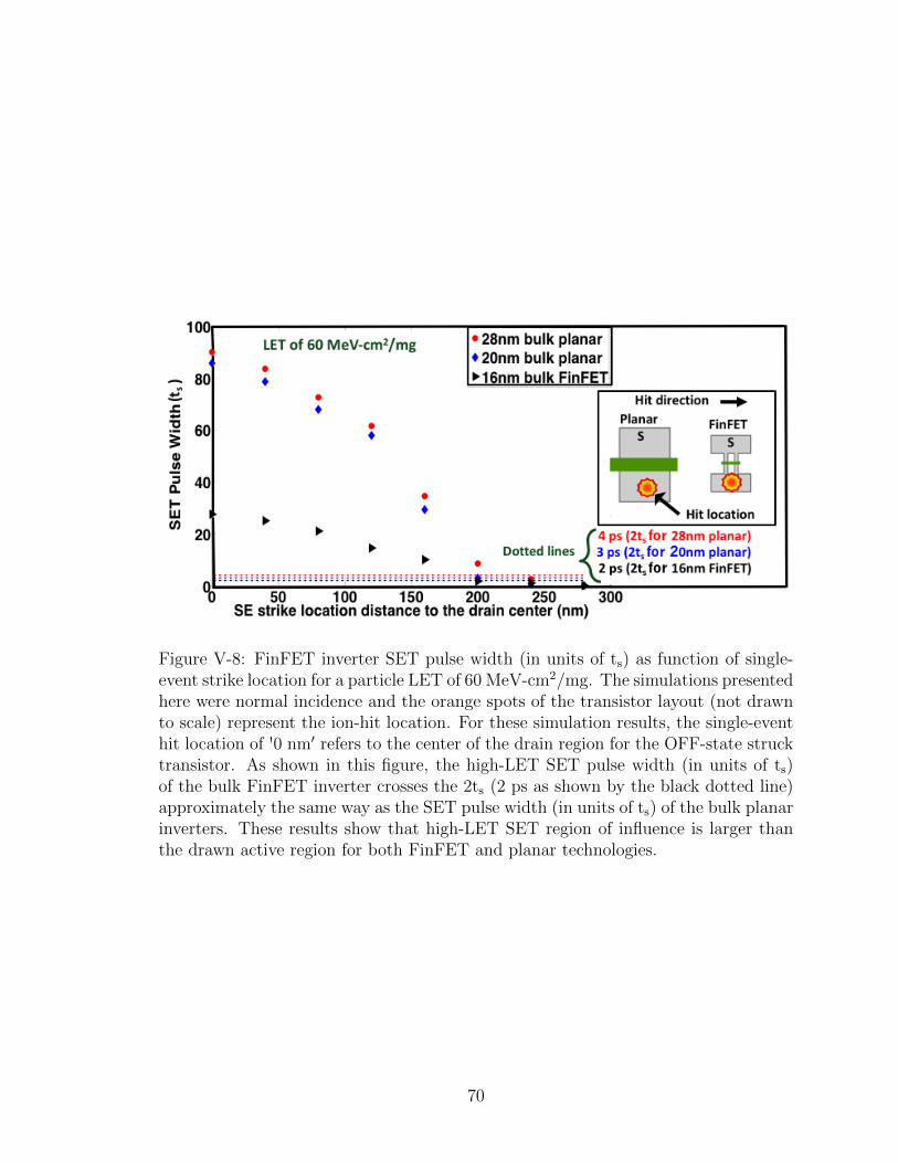
Figure V-8: FinFET inverter SET pulse width (in units of ts) as function of single-event strike location for a particle LET of 60 MeV-cm2/mg. The simulations presentedhere were normal incidence and the orange spots of the transistor layout (not drawnto scale) represent the ion-hit location. For these simulation results, the single-eventhit location of '0 nm′ refers to the center of the drain region for the OFF-state strucktransistor. As shown in this figure, the high-LET SET pulse width (in units of ts)of the bulk FinFET inverter crosses the 2ts (2 ps as shown by the black dotted line)approximately the same way as the SET pulse width (in units of ts) of the bulk planarinverters. These results show that high-LET SET region of influence is larger thanthe drawn active region for both FinFET and planar technologies.
70
OFF-state struck transistor until the SET-induced pulse width (in units of ts) and
the ion hit current value were reduced below the threshold values predefined by the
upset criteria (i.e., the 2ts value and the restoring transistor drive current).
In order to compare 3D TCAD simulation results and experimental data (i.e.,
SE cross section values per FF), the calculated SE cross section of the analyzed FF
circuits are estimated using the inverter sensitive area and the technology area-scaling
factor. Typically, the logic circuit area-scaling factor has been ∼ 0.53 per generation
[Bohr-18]. However, due to the constraints imposed by BEOL scaling (for example,
the metal interconnect scaling of ∼ 0.7 per technology), and the size of I/O pads,
which typically do not scale [Bohr-18, Hoen-15], an area-scaling factor of ∼ 0.49 per
technology node (that is, the area-scaling factor of 0.7 × 0.7 = 0.49 per technology
node) is used in this work. Figure V-9 shows the calculated SE cross sections and
measured SE cross sections for conventional unhardened D flip-flops. The calculated
SE cross section per FF was normalized to the drawn drain area of the minimum size
NMOS transistor. Calculated SE cross sections in Figure V-9 (a) show trends that are
consistent with experimental data in Figure V-9 (b). As a result, the upset criteria
and simulation approaches used here can be helpful to designers and single-event
researchers for the prediction and analysis of SEU cross sections of both advanced
planar and FinFET memory circuits used in space or terrestrial electronics systems.
These SE cross section results also indicate potential charge collection from the
neck region (i.e., sub-fin region) of the FinFET, and even some reduced charge
collection from the silicon substrate region at particle LET between 2.4 MeV-
cm2/mg and LET of 10 MeV-cm2/mg. This charge collection response mechanism
differentiates bulk and SOI FinFET technologies [Ball-10, Roch-13, Ball-18].
71
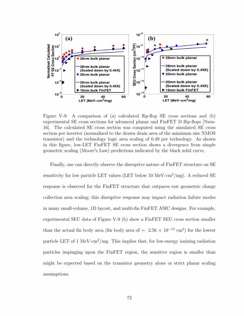
Figure V-9: A comparison of (a) calculated flip-flop SE cross sections and (b)experimental SE cross sections for advanced planar and FinFET D flip-flops [Nsen-16]. The calculated SE cross section was computed using the simulated SE crosssection per inverter (normalized to the drawn drain area of the minimum size NMOStransistor) and the technology logic area scaling of 0.49 per technology. As shownin this figure, low-LET FinFET SE cross section shows a divergence from simplegeometric scaling (Moore's Law) predictions indicated by the black solid curve.
Finally, one can directly observe the disruptive nature of FinFET structure on SE
sensitivity for low particle LET values (LET below 10 MeV-cm2/mg). A reduced SE
response is observed for the FinFET structure that outpaces raw geometric charge
collection area scaling; this disruptive response may impact radiation failure modes
in many small-volume, 1D layout, and multi-fin FinFET ASIC designs. For example,
experimental SEU data of Figure V-9 (b) show a FinFET SEU cross section smaller
than the actual fin body area (fin body area of ∼ 2.56 × 10⁻¹² cm2) for the lowest
particle LET of 1 MeV-cm2/mg. This implies that, for low-energy ionizing radiation
particles impinging upon the FinFET region, the sensitive region is smaller than
might be expected based on the transistor geometry alone or strict planar scaling
assumptions.
72

Conclusions
Upset criteria based on the intrinsic switching behavior of inverter circuits have
been developed in this work. Using these upset criteria and simulated inverter SE
cross section results, experimentally observed trends for SEU cross sections have been
explained and quantified for FF designs fabricated at advanced technology nodes.
This work also quantified the manifestation of the disruptive nature of FinFET
transistor structure on SE sensitivity for low LET values (LET below 10 MeV-
cm2/mg).
In this work, 3D TCAD simulations show a significant reduction of low-LET
FinFET inverter SE cross section (i.e., the inverter SE cross section is on the order of
∼ 35 nm × 35 nm) relative to the SE cross section of a comparable planar inverter
(i.e., the inverter SE cross section is on the order of ∼ 200 nm × 200 nm); explaining
observed experimental data in 16nm FinFET DFF testing. Further, for higher LET
values, the simulated results in this work also explain a lack of reduction of SEU
cross sections with scaling (e.g., ∼ 2× lower SE cross section per FF for the 16nm
bulk FinFET technology compared to bulk planar 20nm and 28nm technologies at a
particle LET of 60 MeV-cm2/mg).
The understanding of the mechanisms leading to a precipitous fall-off of observed
SEU cross-sections for bulk FinFET geometries at low particle LET from that
predicted by simple Moore's Law geometric scaling is particularly important for
accurate prediction of error rates, since circuit error rates are often governed by the
distribution of low LET particles that dominate the space environment. Furthermore,
the upset criteria and analysis methods developed in this work can provide IC
designers with new insights to quickly assess the sensitivity of bulk FinFET circuits
73
to radiation-induced effects and ultimately design better radiation-hardened circuits.
74

CHAPTER VI
ANGULAR EFFECTS ON SINGLE-EVENT MECHANISMS IN BULK FINFETS
Introduction
The discrete structure of FinFETs introduces unique geometric and orientation
dependences for angular single-event mechanisms and single-event upset responses of
FinFET circuits. While SEE-induced failure mechanisms (including both normal
incidence and angular effects) in planar technologies are well understood [Reed-
02, Buch-04, Schw-06, Amus-07, Baze-08, Tipt-08a, Tipt-08b, Amus-09, Nsen-16,
Nsen-17a, Zhan-17], the structure of FinFETs introduces unique geometric and
orientation dependences for angular SE mechanisms and SE responses of FinFET
circuits. Previous work on 14/16nm bulk FinFET designs has shown that the SE
response of bulk FinFET circuits at normal (0◦) incidence strongly depends on the
FinFET structure [Seif-12, Nsen-16, Nsen-17a, Zhan-17]. A detailed discussion of the
impact of FinFET structure on normal incidence SE response of 14/16 bulk FinFETs
is also provided in Chapter V. In addition, Zhang et al. explored the effect of low-tilt-
angle heavy ion incidences on 16nm bulk FinFET D flip-flops (DFFs) [Zhan-17]. The
supporting analysis of [Zhan-17] indicates that angular single-event upset (SEU) cross
section as a function of incident tilt angle (for particle incidences parallel to the fins)
for the 16nm bulk FinFET DFFs follows a similar trend as that of planar technologies.
This SEU response behavior for angled incidences parallel to the fins is attributed
to the increased SE charge chord length in the active Si region as the ion tilt angle
increases [Zhan-17]. However, the understanding and quantification of angular effects
75
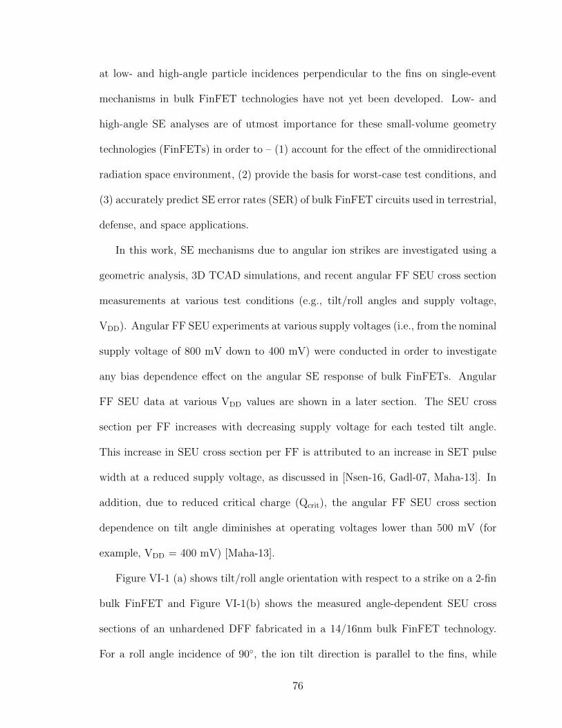
at low- and high-angle particle incidences perpendicular to the fins on single-event
mechanisms in bulk FinFET technologies have not yet been developed. Low- and
high-angle SE analyses are of utmost importance for these small-volume geometry
technologies (FinFETs) in order to – (1) account for the effect of the omnidirectional
radiation space environment, (2) provide the basis for worst-case test conditions, and
(3) accurately predict SE error rates (SER) of bulk FinFET circuits used in terrestrial,
defense, and space applications.
In this work, SE mechanisms due to angular ion strikes are investigated using a
geometric analysis, 3D TCAD simulations, and recent angular FF SEU cross section
measurements at various test conditions (e.g., tilt/roll angles and supply voltage,
VDD). Angular FF SEU experiments at various supply voltages (i.e., from the nominal
supply voltage of 800 mV down to 400 mV) were conducted in order to investigate
any bias dependence effect on the angular SE response of bulk FinFETs. Angular
FF SEU data at various VDD values are shown in a later section. The SEU cross
section per FF increases with decreasing supply voltage for each tested tilt angle.
This increase in SEU cross section per FF is attributed to an increase in SET pulse
width at a reduced supply voltage, as discussed in [Nsen-16, Gadl-07, Maha-13]. In
addition, due to reduced critical charge (Qcrit), the angular FF SEU cross section
dependence on tilt angle diminishes at operating voltages lower than 500 mV (for
example, VDD = 400 mV) [Maha-13].
Figure VI-1 (a) shows tilt/roll angle orientation with respect to a strike on a 2-fin
bulk FinFET and Figure VI-1(b) shows the measured angle-dependent SEU cross
sections of an unhardened DFF fabricated in a 14/16nm bulk FinFET technology.
For a roll angle incidence of 90◦, the ion tilt direction is parallel to the fins, while
76

a roll angle of 0◦ provides an ion tilt direction that is perpendicular to the fins, as
indicated in Figure VI-1(a). The 90◦ roll upset cross section, as a function of tilt
angle, agrees with the supporting analysis provided in [Zhan-17]. The 90◦ roll upset
response behaves like that of planar technologies, where the 90◦ roll cross section
increases with tilt angle due to increased charge chord length in the active silicon
regions.
However, the upset data at a roll angle of 0◦, as shown by the experimentally
observed SEU cross section response in Figure VI-1 (b), clearly shows that there are
different geometrical SE mechanisms at play. This work elucidates these geometric
effects on angular SE mechanisms in bulk FinFET circuits. The geometric effects dis-
cussed in this work are attributed to distinctive structural characteristics of the bulk
FinFET device that can lead to angular dependence in charge deposition/collection
processes and the resulting SEU cross-section responses.
It is also worth noting that this SE angular behavior parallels earlier observations
in bulk silicon germanium (SiGe) heterojunction bipolar transistors (HBTs) [Mars-
00]. While the technology and mechanisms differ, Marshall et al.'s investigations of
bulk SiGe HBTs also show the same type of SE angular asymmetry [Mars-00, Mars-
05]. This observation of the angular SE response is important because of its impact
on error rates [Pete-93, Conn-95, Mars-00, Mars-05].
Angular SE Mechanisms in Bulk FinFETs
A geometric analysis of angular SE mechanisms has been developed and is
demonstrated using a 2-fin bulk FinFET structure. While a 2-fin bulk FinFET
structure, shown in Figure VI-1 (a), is used to illustrate the underlying angular
77
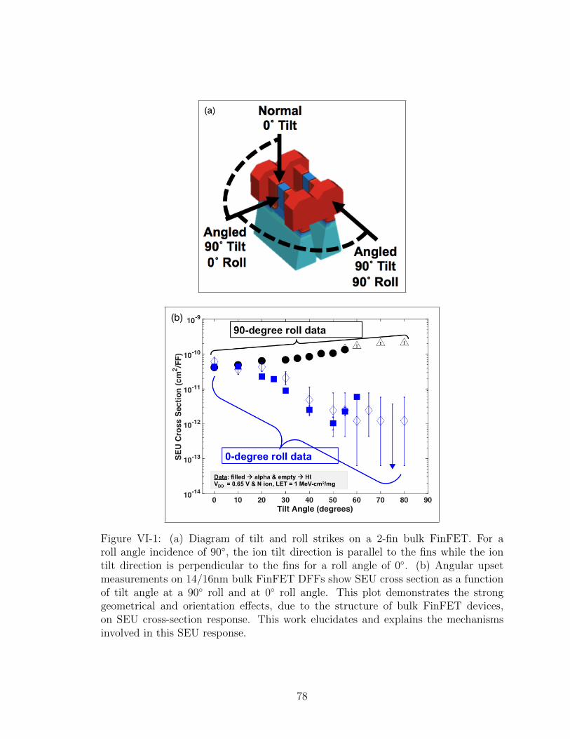
Figure VI-1: (a) Diagram of tilt and roll strikes on a 2-fin bulk FinFET. For aroll angle incidence of 90◦, the ion tilt direction is parallel to the fins while the iontilt direction is perpendicular to the fins for a roll angle of 0◦. (b) Angular upsetmeasurements on 14/16nm bulk FinFET DFFs show SEU cross section as a functionof tilt angle at a 90◦ roll and at 0◦ roll angle. This plot demonstrates the stronggeometrical and orientation effects, due to the structure of bulk FinFET devices,on SEU cross-section response. This work elucidates and explains the mechanismsinvolved in this SEU response.
78
mechanisms, extension to a bulk FinFET structure with more than two fins is straight-
forward. In this analysis, the 2-fin bulk FinFET structure is appropriate because the
integrated circuit (IC) designs used to corroborate these angular mechanisms utilize
2-fin FinFET devices. Figure VI-2 (a) depicts a 3D view of the 2-fin bulk FinFET.
A two-dimensional (2D) cut from the top fin surface down to the substrate of the
transistor results in the 2D transistor cross-section view shown in Figure VI-2 (b).
Some of the critical FinFET dimensions required for the geometric analysis are shown
on the 2D cut view in Figure VI-2 (b).
The parameter, Tfin is the top fin width, TS is the bottom fin width (i.e., the
silicon interface of the fin body with the sub-fin bulk structure), respectively. For a
rectangular shaped fin, Tfin ≈ TS. However, if a nonrectangular fin (e.g., a trapezoidal
fin or tri-gate [Seif-12]) is considered, top and bottom fin width dimensions are
unequal and usually, Tfin < TS. The fin height (Hfin), the spacing between the nearest
edges of the two fins (Xf), as well as the spacing between the nearest edges of the
two sub-fin structures (XS) are also shown in Figure VI-2 (b). Reasonable estimates
of these dimensions can be obtained from the Arizona State University predictive
technology model [Ariz-18].
Analysis of 0◦ Roll Angular SE Mechanisms
When an energetic ionizing particle penetrates any semiconductor material, it
liberates an ionizing trail of free electron-hole pairs in the target material. Under
certain conditions (i.e., bias, strike location, angle of incidence, etc.), the extraneous
SE-induced charge can lead to the disturbance of the normal IC operation and cause a
soft error. Whether a particle deposits enough charge to cause an upset is dependent
79
Figure VI-2: (a) Example of 3D view and (b) 2D cross section view for a 2-fin bulkFinFET structure. Tfin is the top fin width and TS is the bottom fin width. Hfin isthe fin height, Xf the spacing between the nearest edges of the two fins, and XS is thespacing between the nearest edges of the two sub-fin structures.
80

on both linear energy transfer (LET) of the particle and its particular path length
(i.e., SE charge chord length) through the sensitive volume [Mass-93]. In this work,
SE-induced deposited charge (or the SE charge chord length) in the active Si regions
of the bulk FinFETs is used to explain and compare SE mechanisms for angular
effects in bulk FinFETs. A geometric analysis utilizing the amount of deposited
charge, Qdep in the fin structure and/or sub-fin structure, as a critical parameter,
elucidates four separate charge deposition mechanisms, as illustrated in Figure VI-3.
The angle θi (with i, being an integer 1 ≤ i ≤ 4) represents the upper-bound angle
or the tilt angle for transitioning from one Qdep region to another. The angles α and
β are intermediate angles used to calculate θi. While the upper-bound angle (θi) is
fairly well defined by the incident particle, the intermediate angles can move quite a
bit depending on the vertical entry location of the incident particle. As a result, only
values of θi are shown in Figure VI-3.
Mechanism (1): 0◦ ≤ θ ≤ θ1 (Fin/sub-fin Qdep)
This is the most straightforward case for angular SE mechanisms in bulk FinFETs
and is characterized by combined charge deposition in both fin structure and sub-fin
structures. The maximum charge deposition in both fin and sub-fin regions occurs
at normal (0◦) incidence, where the particle charge chord length equals the sum of
the fin height and the sub-fin height. Figure VI-3 (a) highlights this mechanism (1).
Additionally, this mechanism corresponds to very low tilt angles of incidence (from 0◦
incidence up to a tilt angle, θ1). The angle θ1 is the upper-bound angle or the tilt angle
at which the deposited charge in the fin and sub-fin regions starts to decrease due
to a reduction in particle chord length inside the active Si. Utilizing the previously
81

discussed geometrical parameters, θ1 has been calculated to be approximately 20◦.
Mechanism (1) implies that the angular SEU cross-section response of bulk FinFETs is
the highest at normal incidence and starts to decrease at a tilt angle of approximately
20◦.
Mechanism (2): θ1 ≤ θ ≤ θ2 (Reduced fin/sub-fin Qdep)
The chord length inside the fin structure and the sub-fin structure reduces as the
tilt angle of incidence increases beyond θ1. With a reduction in chord length, Qdep is
also reduced in this region. The upper-bound angle for this mechanism, θ2, is defined
as the angle where the ion passes through the maximum distance in one fin but does
not pass through the second fin. This angle has been calculated to be approximately
50◦, as shown in Figure VI-3 (b). The reduction of Qdep in this mechanism (2)
elucidates the reduction in SEU cross section observed over this tilt angle range, as
seen in Figure VI-1 (b).
Mechanism (3): θ2 ≤ θ ≤ θ3 (2-fin Qdep & further reduced sub-fin Qdep)
Contrary to mechanism (2), the angular range of mechanism (3) is associated
with an increase in Qdep. While the sub-fin Qdep is further reduced, this reduction
is compensated by the charge deposition in the second fin, as shown in Figure VI-3
(c). In this region the SEU cross section shows gradual increase with tilt angle. The
upper-bound angle for this mechanism, θ3, has been calculated to be approximately
65◦.
82

Mechanism (4): θ ≥ θ3 (2-fin Qdep, but no sub-fin Qdep)
This mechanism corresponds to a very high tilt angle of incidence, which is
characterized by Qdep in both fins, but the ion path no longer traverses the sub-fin
region. This mechanism is characterized by charge deposition only in the fin structure.
If the deposited charge is greater than the critical charge of the circuit under test, an
upset will occur. However, for ions with a low LET value it is conceivable that the
charge deposited in the fins only is too small to cause an upset.
Figure VI-3: Geometric analyses of charge deposition mechanisms as a function oftilt angle in 14/16nm bulk FinFETs at a fixed 0◦ roll angle. Four different chargedeposition mechanisms are at play for this 0◦ roll angle – (a) Mechanism (1): Fin/sub-fin Qdep; (b) Mechanism (2): Reduced fin/sub-fin Qdep. The angle β is an intermediateangle used to calculate θ2; (c) Mechanism (3): 2-fin Qdep and further reduced sub-finQdep. The angle α is an intermediate angle used to calculate θ3; (d) Mechanism (4):2-fin Qdep, but no sub-fin Qdep. The angular distributions for these mechanisms are(a) Mechanism (1): 0◦ ≤ θ ≤ 20◦; (b) Mechanism (2): 20◦ ≤ θ ≤ 50◦; (c) Mechanism(3): 50◦ ≤ θ ≤ 65◦; and (d) Mechanism (4): θ ≥ 65◦.
83

Analysis of 90◦ Roll Angular SE Mechanism
The 90◦ roll angle (i.e., ion trajectory is parallel to the fins for non-normal angles
of incidence) follows a similar charge deposition mechanism as observed in planar
technologies, where the deposited charge increases with tilt angle of incidence. This
implies that the 90◦ roll charge chord length continuously increases with tilt angle
(with the limitation that the tilt angle induced ion path remains within the fin/sub-fin
regions), as shown in Figure VI-4. This 90◦ roll mechanism will result in an increase
in angular upset cross section data for bulk FinFET designs irradiated at a 90◦ roll
angle.
Figure VI-4: (a) 3D view of a bulk FinFET showing the cut line. (b) 2D cross sectionview of the bulk FinFET. Charge deposition mechanisms for 90◦ roll angle. The 90◦
roll charge chord length continuously increases with tilt angle.
84
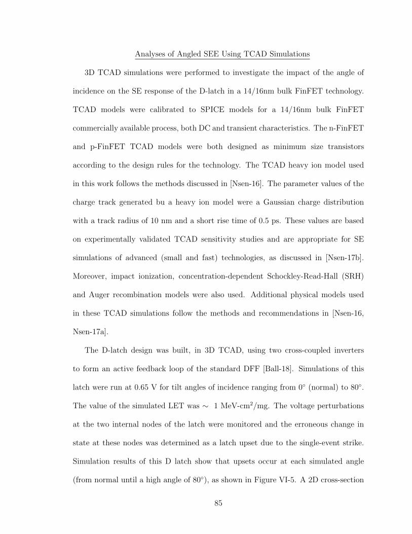
Analyses of Angled SEE Using TCAD Simulations
3D TCAD simulations were performed to investigate the impact of the angle of
incidence on the SE response of the D-latch in a 14/16nm bulk FinFET technology.
TCAD models were calibrated to SPICE models for a 14/16nm bulk FinFET
commercially available process, both DC and transient characteristics. The n-FinFET
and p-FinFET TCAD models were both designed as minimum size transistors
according to the design rules for the technology. The TCAD heavy ion model used
in this work follows the methods discussed in [Nsen-16]. The parameter values of the
charge track generated bu a heavy ion model were a Gaussian charge distribution
with a track radius of 10 nm and a short rise time of 0.5 ps. These values are based
on experimentally validated TCAD sensitivity studies and are appropriate for SE
simulations of advanced (small and fast) technologies, as discussed in [Nsen-17b].
Moreover, impact ionization, concentration-dependent Schockley-Read-Hall (SRH)
and Auger recombination models were also used. Additional physical models used
in these TCAD simulations follow the methods and recommendations in [Nsen-16,
Nsen-17a].
The D-latch design was built, in 3D TCAD, using two cross-coupled inverters
to form an active feedback loop of the standard DFF [Ball-18]. Simulations of this
latch were run at 0.65 V for tilt angles of incidence ranging from 0◦ (normal) to 80◦.
The value of the simulated LET was ∼ 1 MeV-cm2/mg. The voltage perturbations
at the two internal nodes of the latch were monitored and the erroneous change in
state at these nodes was determined as a latch upset due to the single-event strike.
Simulation results of this D latch show that upsets occur at each simulated angle
(from normal until a high angle of 80◦), as shown in Figure VI-5. A 2D cross-section
85
plot of carrier distribution, after the single event, clearly highlights the effect of a
singly angled ion as it passes through one fin to another fin/neck (sub-fin) region,
depositing charge only in the active silicon region. The geometric analysis described
in this chapter shows good agreement with the results of the TCAD simulations. The
simulated charge chord length (i.e., the SE-induced chord length indicated by the
carrier distribution region other than the blue-colored intrinsic doping concentration
in Figure VI-5) correlates with the Qdep regions predicted by the geometrical analysis
in earlier section of this work. Moreover, TCAD simulations of the D latch circuit
resulted in an upset response at simulated tilt angles (i.e., 0◦, 30◦, and 60◦), except
at a tilt angle of 80◦. For the 80◦ tilt angle, the charge deposited in the fins only is
too small to cause an upset. However, for TCAD simulation analyses, the ion entry
location can be varied vertically in order to explore the minimum Qdep required to
cause an upset at very high tilt angles.
Figure VI-5: Simulated SEU results for angled strikes on a full 3D TCAD 14/16nmbulk FinFET (2-fin) latch at a fixed 0◦ roll angle and VDD of 0.65 V. The blue-colored doping concentration of the 2D Qdep profiles corresponds to the intrinsicdoping concentration of the simulated bulk FinFET. As shown in this figure, simulatedangular upset responses correlate with angular SE mechanisms elucidated by thedeveloped geometric analysis [Nsen-18].
86
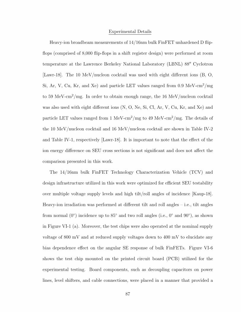
Experimental Details
Heavy-ion broadbeam measurements of 14/16nm bulk FinFET unhardened D flip-
flops (comprised of 8,000 flip-flops in a shift register design) were performed at room
temperature at the Lawrence Berkeley National Laboratory (LBNL) 88′′ Cyclotron
[Lawr-18]. The 10 MeV/nucleon cocktail was used with eight different ions (B, O,
Si, Ar, V, Cu, Kr, and Xe) and particle LET values ranged from 0.9 MeV-cm2/mg
to 59 MeV-cm2/mg. In order to obtain enough range, the 16 MeV/nucleon cocktail
was also used with eight different ions (N, O, Ne, Si, Cl, Ar, V, Cu, Kr, and Xe) and
particle LET values ranged from 1 MeV-cm2/mg to 49 MeV-cm2/mg. The details of
the 10 MeV/nucleon cocktail and 16 MeV/nucleon cocktail are shown in Table IV-2
and Table IV-1, respectively [Lawr-18]. It is important to note that the effect of the
ion energy difference on SEU cross sections is not significant and does not affect the
comparison presented in this work.
The 14/16nm bulk FinFET Technology Characterization Vehicle (TCV) and
design infrastructure utilized in this work were optimized for efficient SEU testability
over multiple voltage supply levels and high tilt/roll angles of incidence [Kaup-18].
Heavy-ion irradiation was performed at different tilt and roll angles – i.e., tilt angles
from normal (0◦) incidence up to 85◦ and two roll angles (i.e., 0◦ and 90◦), as shown
in Figure VI-1 (a). Moreover, the test chips were also operated at the nominal supply
voltage of 800 mV and at reduced supply voltages down to 400 mV to elucidate any
bias dependence effect on the angular SE response of bulk FinFETs. Figure VI-6
shows the test chip mounted on the printed circuit board (PCB) utilized for the
experimental testing. Board components, such as decoupling capacitors on power
lines, level shifters, and cable connections, were placed in a manner that provided a
87
clear beam path at high angles of incidence, corresponding to the clear paths on the
TCV [Kaup-18].
Figure VI-6: The IC test structure used for angular irradiations. (a) The IC testprinted circuit board (PCB) showing no obstructions to beam path, for high tilt anglesof incidence from the top and left edges of the PCB. The Teensy 3.2 microcontrollerboard is visible on the right edge of the PCB. (b) A picture of the test chip elevatedon gold spacers with bond wires on only two sides of the die. The DUT was packagedon gold plate spacers, which placed the DUT above the edge of the package cavity,providing an unobstructed path on two sides for the ion beam at high tilt angles ofincidence [Kaup-18].
Experimental Results and Discussions
0◦ Roll FF SEU Cross Sections
The analysis of 0◦ roll SEU cross section shows that high-LET (i.e., Cu ion with
LET of 21 MeV-cm2/mg) SEU cross section as a function of incident tilt angle does
not change significantly, as shown in Figure VI-7. This upset cross section behavior at
88
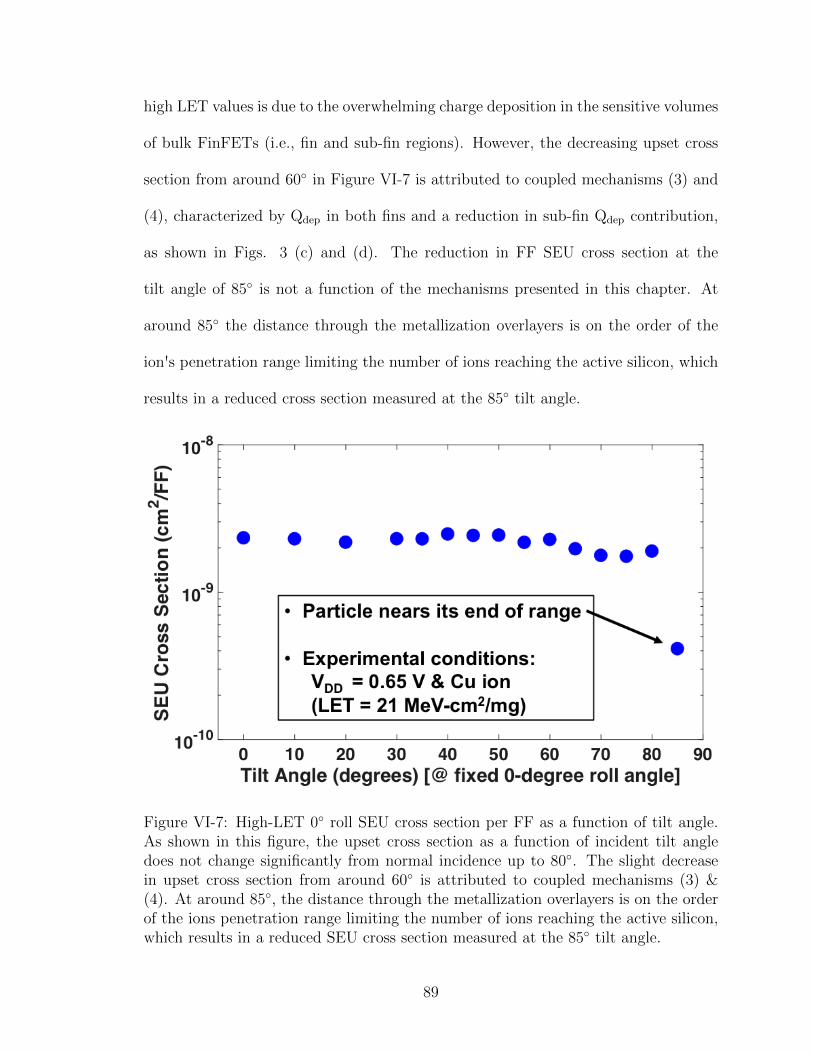
high LET values is due to the overwhelming charge deposition in the sensitive volumes
of bulk FinFETs (i.e., fin and sub-fin regions). However, the decreasing upset cross
section from around 60◦ in Figure VI-7 is attributed to coupled mechanisms (3) and
(4), characterized by Qdep in both fins and a reduction in sub-fin Qdep contribution,
as shown in Figs. 3 (c) and (d). The reduction in FF SEU cross section at the
tilt angle of 85◦ is not a function of the mechanisms presented in this chapter. At
around 85◦ the distance through the metallization overlayers is on the order of the
ion's penetration range limiting the number of ions reaching the active silicon, which
results in a reduced cross section measured at the 85◦ tilt angle.
Figure VI-7: High-LET 0◦ roll SEU cross section per FF as a function of tilt angle.As shown in this figure, the upset cross section as a function of incident tilt angledoes not change significantly from normal incidence up to 80◦. The slight decreasein upset cross section from around 60◦ is attributed to coupled mechanisms (3) &(4). At around 85◦, the distance through the metallization overlayers is on the orderof the ions penetration range limiting the number of ions reaching the active silicon,which results in a reduced SEU cross section measured at the 85◦ tilt angle.
89

The low-LET SEU cross sections, as a function of tilt angle and a fixed 0◦ roll
angle for a particle LET of 1 MeV-cm2/mg (i.e., N ion), are shown in Figure VI-
8. In addition to the SEU cross section curve, the geometrical representations and
transition angles from the geometric analysis are provided for reference. The low-LET
SEU cross section, as a function of tilt angle and a fixed 0◦ roll angle, demonstrate the
proposed strong dependence on the FinFET geometry. In Figure VI-8, it is evident
that the upset cross section per FF is the highest at normal incidence and starts to
decrease at around 20◦ due to mechanism (2), which is characterized by a reduction
in fin/sub-fin Qdep.
At around 50◦ tilt angle, the alpha particle SEU cross section starts to increase
again due to mechanism (3), which is characterized by the ion charge chord length
through two fins of the bulk FinFET device and some charge deposition in the sub-
fin/bulk region. No alpha particle upsets were observed at a tilt angle greater than 60◦
because the alpha particle nears its end of range at around 60◦ tilt angle. However, for
heavy ion SEU measurements, the change in SEU cross section for this angular region
(3) is within the error bars. It is worth noting that the plotted error bars in Figure
VI-8 represent 95% Poisson confidence interval of the recorded SEU measurements
[Gehr-86]. The disparity between alpha particle SEU cross section and heavy ion
SEU cross section trends as a function of tilt angle is attributed to poor statistics of
heavy ion SEU measurements as indicated by the long heavy ion error bars in this
angular region (3). Further analysis and additional heavy ion SEU test data with
better statistics are recommended in order to fully understand the SEU cross section
behavior in this angular region (3). Nonetheless, the geometric analysis in Figure VI-
3 (c) and calculated charge chord length values in Figure VI-9 show that the charge
90
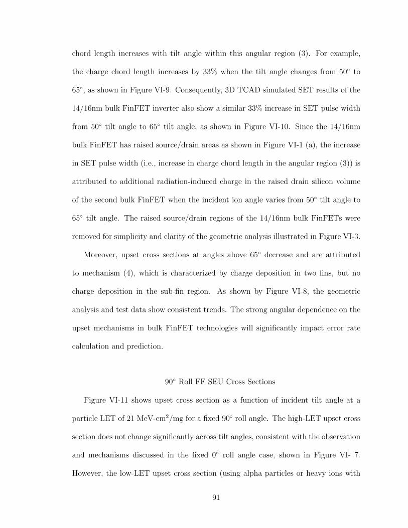
chord length increases with tilt angle within this angular region (3). For example,
the charge chord length increases by 33% when the tilt angle changes from 50◦ to
65◦, as shown in Figure VI-9. Consequently, 3D TCAD simulated SET results of the
14/16nm bulk FinFET inverter also show a similar 33% increase in SET pulse width
from 50◦ tilt angle to 65◦ tilt angle, as shown in Figure VI-10. Since the 14/16nm
bulk FinFET has raised source/drain areas as shown in Figure VI-1 (a), the increase
in SET pulse width (i.e., increase in charge chord length in the angular region (3)) is
attributed to additional radiation-induced charge in the raised drain silicon volume
of the second bulk FinFET when the incident ion angle varies from 50◦ tilt angle to
65◦ tilt angle. The raised source/drain regions of the 14/16nm bulk FinFETs were
removed for simplicity and clarity of the geometric analysis illustrated in Figure VI-3.
Moreover, upset cross sections at angles above 65◦ decrease and are attributed
to mechanism (4), which is characterized by charge deposition in two fins, but no
charge deposition in the sub-fin region. As shown by Figure VI-8, the geometric
analysis and test data show consistent trends. The strong angular dependence on the
upset mechanisms in bulk FinFET technologies will significantly impact error rate
calculation and prediction.
90◦ Roll FF SEU Cross Sections
Figure VI-11 shows upset cross section as a function of incident tilt angle at a
particle LET of 21 MeV-cm2/mg for a fixed 90◦ roll angle. The high-LET upset cross
section does not change significantly across tilt angles, consistent with the observation
and mechanisms discussed in the fixed 0◦ roll angle case, shown in Figure VI- 7.
However, the low-LET upset cross section (using alpha particles or heavy ions with
91
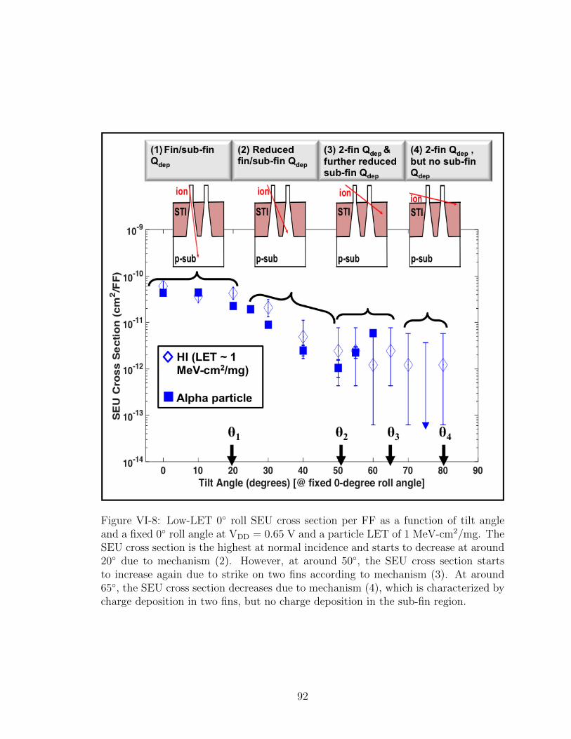
Figure VI-8: Low-LET 0◦ roll SEU cross section per FF as a function of tilt angleand a fixed 0◦ roll angle at VDD = 0.65 V and a particle LET of 1 MeV-cm2/mg. TheSEU cross section is the highest at normal incidence and starts to decrease at around20◦ due to mechanism (2). However, at around 50◦, the SEU cross section startsto increase again due to strike on two fins according to mechanism (3). At around65◦, the SEU cross section decreases due to mechanism (4), which is characterized bycharge deposition in two fins, but no charge deposition in the sub-fin region.
92
Figure VI-9: Normalized charge chord length as a function of tilt angle (with a fixed0◦ roll angle) for the 14/16nm bulk FinFET in the angular region (3). Calculatedchord lengths in this figure are normalized to the chord length value at 65◦ tilt angle.
an LET of approximately 1 MeV-cm2/mg) at a 90◦ roll angle increases with tilt angle,
as shown in Figure VI-12. The increase in upset cross section is due to an increase
in the distance traversed by the ion, and therefore the deposited charge, when the
particle hits the bulk FinFET at an angle parallel to the fins, as explained in Figure
VI-4. The 90◦ roll angle upset cross section behavior is similar to that of planar
technologies, as discussed in [Zhan-17].
93
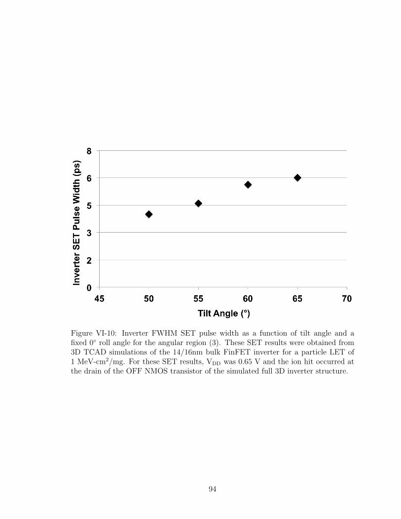
Figure VI-10: Inverter FWHM SET pulse width as a function of tilt angle and afixed 0◦ roll angle for the angular region (3). These SET results were obtained from3D TCAD simulations of the 14/16nm bulk FinFET inverter for a particle LET of1 MeV-cm2/mg. For these SET results, VDD was 0.65 V and the ion hit occurred atthe drain of the OFF NMOS transistor of the simulated full 3D inverter structure.
94
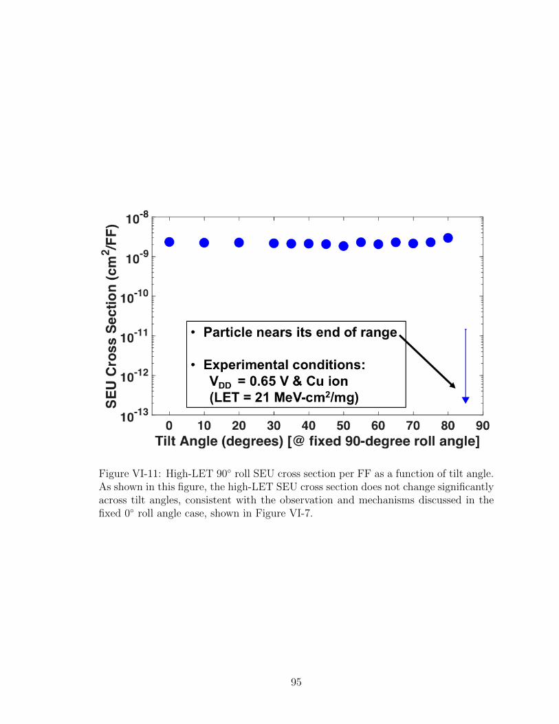
Figure VI-11: High-LET 90◦ roll SEU cross section per FF as a function of tilt angle.As shown in this figure, the high-LET SEU cross section does not change significantlyacross tilt angles, consistent with the observation and mechanisms discussed in thefixed 0◦ roll angle case, shown in Figure VI-7.
95

Figure VI-12: Low-LET 90◦ roll SEU cross section per FF as a function of tilt angle.As shown in this figure, low-LET 90◦ roll angle upset cross section increases with tiltangle due to an increase in charge chord length in the active Si region of the bulkFinFET.
96
Impact of Supply Voltage on Angular SEU Cross Sections
As device dimensions and operating voltage for modern technologies are reduced,
the sensitivity to SE radiation can increase dramatically [Maha-13]. Therefore, it is
important to investigate the effect of supply voltage on the angular effects of FF upset
cross section. Figure VI-13 (a) shows alpha SEU cross section for a fixed 0◦ roll angle
and Figure VI-13 (b) shows alpha SEU cross section for a fixed 90◦ roll angle, over
a range of tilt angles, from 0◦ to 70◦. For both roll angle conditions, four different
supply voltages (i.e., 0.4 V, 0.5 V, 0.65 V, and nominal voltage or 0.8 V) were applied
to examine the impact of supply voltage on the angular response. As shown in Figure
VI-13 (a) and (b), the SEU cross section dependence on tilt angle decreases with
reduced voltage supply due to reduced critical charge, Qcrit [Maha-13]. In addition,
SEU cross section at one tilt angle of incidence increases with reduced supply voltage,
as shown in Figure VI-13. For example, the upset cross section at the lower supply
voltage (i.e., VDD = 0.4 V) shows a SEU cross-section increase of more than one order
of magnitude compared to the upset cross section at the nominal supply voltage of
0.8 V. This increase in SEU cross section per FF is due to an increase in SET pulse
width at a reduced supply voltage [Gadl-07, Maha-13, Nsen-16, Nsen-18].
97
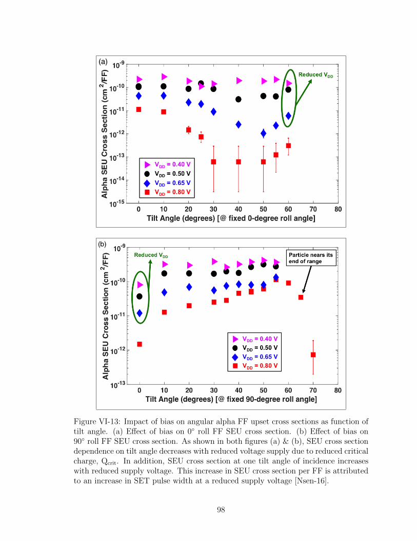
Figure VI-13: Impact of bias on angular alpha FF upset cross sections as function oftilt angle. (a) Effect of bias on 0◦ roll FF SEU cross section. (b) Effect of bias on90◦ roll FF SEU cross section. As shown in both figures (a) & (b), SEU cross sectiondependence on tilt angle decreases with reduced voltage supply due to reduced criticalcharge, Qcrit. In addition, SEU cross section at one tilt angle of incidence increaseswith reduced supply voltage. This increase in SEU cross section per FF is attributedto an increase in SET pulse width at a reduced supply voltage [Nsen-16].
98
Conclusions
Angular SEU testing of 14/16nm bulk FinFET D-flip-flops exhibits strong geomet-
ric and orientation dependences, with normal incident strikes being the worst case.
Geometric analyses and 3D TCAD simulation results of bulk FinFETs effectively
explain upset mechanisms behind experimentally observed angular upset cross-section
responses, and the difference in response for 0◦ and 90◦ roll angles, for conventional
unhardened DFFs. The results show that angular upset cross section characteristics
can be attributed to different charge deposition regions in the fin and the sub-fin bulk
structures. Insights of this study advance the understanding of the overall angular
upset behavior of bulk FinFETs and accounting for these angular effects is critical
when calculating/predicting error rates of bulk FinFETs circuits.
99
CHAPTER VII
CONCLUSIONS AND COMMUNITY IMPACT
The change from planar transistor structure to FinFET structure has introduced
new considerations in terms of radiation-induced charge collection processes and
the resulting single-event response of modern circuits. This work characterized the
impact of bulk CMOS FinFET structure on physical SEU mechanisms and effectively
explained experimentally observed SEU responses of bulk FinFET circuits. 3D TCAD
simulations and experimental data were used to analyze SE failure mechanisms and
soft error modes of advanced bulk planar circuits and bulk FinFET circuits.
The use of 3D TCAD tools for single-event simulation analyses of advanced bulk
CMOS technologies has been re-examined. The dimension of the dense tracks are on
the order of key feature sizes of the active devices (channel lengths and fin widths),
and the time frame is on the order of switching time of advanced digital circuits. This
work demonstrated the sensitivity of simulation results to spatial and temporal model
parameters. Simulated upset thresholds using single-event model parameter values
suitable for 14/16nm bulk FinFETs produced a good agreement with experimental
upset thresholds. For example, a thorough SE sensitivity study case using 3D TCAD
14/16nm bulk FinFET inverter and 14/16nm bulk FinFET D latch circuit showed
that the use of a small ion track radius (i.e., the spatial parameter, R) on the order of
R ≤ 20 nm and a short rise time (i.e., the temporal parameter, T) on the order of T
< 2 ps is crucial to resulted in simulation results that are in agreement with historical
critical charge scaling trends and measured upset LET thresholds. The insights of this
100
work will allow RHBD design engineers to quickly assess the single-event sensitivity
of their designs to spatial and temporal model parameters in order to make better
SEE mitigation decisions and accurately calculate error rates.
Moreover, the SEU cross section response of advanced bulk planar technologies
(e.g., 20nm and 28nm technology nodes) and 14/16nm bulk FinFET technologies
have been compared in this work. Simulation analyses and heavy-ion broadbeam
measurements indicate minimal difference in SEU cross sections between 14/16nm
bulk FinFET flip-flops and 20/28nm planar flip-flops for high LET particles. However,
the SEU cross section improvement of bulk FinFET technologies is most evident at
low LET values. Results show that 14/16nm bulk FinFET flip-flops have considerably
lower SEU cross sections than their sub-32nm planar counterparts for particle LET
values less than 10 MeV-cm2/mg. The understanding of this divergence of low-LET
FinFET cross sections from simple geometric scaling predictions is very important for
accurate determination of the contribution of low-LET particles to the overall error
rate of bulk FinFET designs.
A set of upset criteria based on circuit characteristic switching time frame was
also developed and used to bridge transistor-level TCAD simulations to circuit-level
single-event upset cross sections of advanced digital circuits. Interpretation of the
measured and calculated SEU cross section responses of bulk planar circuits and
bulk FinFET circuits using the developed upset criteria quantitatively explained the
observed divergence of low-LET FinFET cross sections from simple geometric scaling
predictions. Comparisons of measured single-event cross sections and computed
single-event cross section responses at normal incidence showed excellent agreement.
Furthermore, angular effects on single-event mechanisms in 14/16nm bulk FinFET
101
technologies have been characterized. Geometric analyses and 3D TCAD simulation
results of bulk FinFETs effectively explain upset mechanisms behind experimentally
observed angular upset cross-section responses, and the difference in response for
0◦ and 90◦ roll angles, for conventional unhardened flip-flops. The results show
that angular upset cross section characteristics can be attributed to different charge
deposition regions in the fin and the sub-fin bulk structures. Insights of this study
advance the understanding of the overall angular upset behavior of bulk FinFETs
and accounting for these angular effects is critical when calculating/predicting error
rates of bulk FinFETs circuits.
The following are important contributions provided by this dissertation:
1) New spatial and temporal considerations for analysis of SE mechanisms in bulk
FinFET technologies have been identified. Physically based arguments and sensitivity
study analyses were presented for justification of appropriate model parameter
choices.
2) The SEU responses of advanced bulk planar and bulk FinFET technologies
have been compared. The manifestation of the disruptive nature of FinFET transistor
structure on SE sensitivity for low LET values (LET below 10 MeV-cm2/mg) has also
been quantified.
3) Bulk FinFET structural effects on SE cross sections for normal incident particles
have been investigated and quantified.
4) A set of upset criteria, which bridge transistor-level SE response to circuit-level
upset cross section response has been developed. The upset criteria and 3D TCAD
simulations methods were utilized to explain SE response of bulk FinFET compared
to bulk planar technologies.
102
5) Angular dependence (up to 90◦ roll angle and up to 85◦ tilt angle) of SEU re-
sponses of 14/16nm bulk FinFETs have been characterized and analyzed. The unique
geometric and orientation dependence of angular single-event mechanisms/single-
event responses of bulk FinFETs have also been analyzed and quantified.
The research presented in this dissertation directly impacts SEE circuit qual-
ification and analysis techniques for advanced technologies. The findings of this
work can be useful to device/circuit designers and the radiation-induced community
in general, for accurate SE characterization and prediction of bulk FinFET digital
circuits intended to perform in terrestrial and space radiation environments. Insights
of this study are applicable to other advanced technologies characterized by discrete
structural features (e.g., 32nm PDSOI, 22nm FDSOI, 7nm bulk FinFETs, nanowires,
etc.). The understanding of these soft error modes and mechanisms discussed in this
dissertation also enables risk reduction in RHBD design and allows accurate error
rate calculations of terrestrial and defense/pace applications.
103
REFERENCES
[Adam-18] J. H. Adams, Jr., A. F. Barghouty, M. H. Mendenhall, R. A. Reed, B. D.Sierawski, K. M. Warren, J. W. Watts, and R. A. Weller, “CREME.” Accessed:Jan. 5, 2018. Available: [Online]. Available: https://creme.isde.vanderbilt.edu.
[Agos-03] S. Agostinelli, et al., “Geant4-a simulation toolkit,” Nucl. Instrum.Methods Phys. Res. A, vol. A506, no. 3, pp. 250–303, Mar. 2003.
[Akke-05] A. Akkerman, J. Barak, and D. Emfietzoglou, “Ion and electron track-structure and its effects in silicon: Model and calculations,” Nucl. Instrum.Meth. Phys. Res. B, vol. 227, no. 3, pp. 319–336, Jan. 2005.
[Allen-59] J. A. Van Allen, C. E. McIlwain, and G. H. Ludwig, “Radiationobservations with satellite 1958 EX,” J. Geophys. Res., vol. 64, no. 3, pp.271–286, Mar. 1959.
[Amus-07] O. A. Amusan, L. W. Massengill, M. P. Baze, B. L. Bhuva, A. F. Witulski,S. DasGupta, A. L. Sternberg, P. R. Fleming, C. C. Heath, and M. L. Alles.,“Directional sensitivity of single event upsets in 90 nm CMOS due to chargesharing,” IEEE Trans. Nucl. Sci., vol. 54, no. 6, pp. 2584–2589, Dec. 2007.
[Amus-09] O. A. Amusan, L. W. Massengill, M. P. Baze, B. L. Bhuva, A. F. Witulski,J. D. Black, A. Balasubramanian, M. C. Casey, D. A. Black, J. R. Ahlbin, R.A. Reed, and M. W. McCurdy, “Mitigation techniques for single-event-inducedcharge sharing in a 90-nm bulk CMOS process,” IEEE Trans. on Device andMater. Rel., vol. 9, pp. 311–317, Jun. 2009.
[Ariz-18] Arizona State University (ASU) Predictive Technology Model (PTM),Accessed: Jan. 5, 2018. [Online]. Available: http://ptm.asu.edu.
[Arto-10] L. Artola, G. Hubert, S. Duzellier, and F. Bezerra, “Collected chargeanalysis for a new transient model by TCAD simulations in 90 nm technology,”IEEE Trans. Nucl. Sci., vol. 57, no. 4, pp. 1869–1875, Aug. 2010.
[Arto-15] L. Artola, M. Gaillardin, G. Hubert, M. Raine, and P. Paillet, “Modelingsingle-event transients in advanced devices and ICs,” IEEE Trans. Nucl. Sci.,vol. 62, no. 4, pp. 1528–1539, Aug. 2015.
[Atki-11] N. M. Atkinson, J. R. Ahlbin, A. F. Witulski, et al. “Effect of transistordensity and charge sharing on single-event transients in 90-nm bulk CMOS,”IEEE Trans. Nucl. Sci., vol. 58, no. 6, pp. 2578–2584, Dec. 2011.
[Auth-12] C. Auth et al., “A 22 nm high performance and low-power CMOStechnology featuring fully-depleted tri-gate transistors, self-aligned contacts andhigh density MIM capacitors,” in Proc. VLSI Technol. Symp. Dig. Tech.Papers, pp. 131–132, Jun. 2012.
104
[Ball-10] D. R. Ball, M. L. Alles, R. D. Schrimpf, and S. Cristoloveanu, “Comparingsingle event upset sensitivity of bulk vs. SOI based FinFET SRAM cellsusing TCAD simulations,” in Proc. IEEE SOI Conf., Oct. 2010, doi:10.1109/SOI.2010.5641058.
[Ball-18] D. R. Ball, M. L. Alles, J. S. Kauppila, R. C. Quinn, J. A. Maharrey,P. Nsengiyumva, T. D. Haeffner, J. D. Rowe, A. L. Sternberg, E. X. Zhang,B. L. Bhuva, and L. W. Massengill, “The impact of charge collection volumeand parasitic capacitance on SEU in SOI and bulk FinFET D flip-flops,” IEEETrans. on Nucl. Sci., vol. 65, no. 1, pp. 326–330, Jan. 2018.
[Bart-03] J. L. Barth, C. S. Dyer, and E. G. Stassinopoulos, “Space, atmospheric,and terrestrial radiation environments,” IEEE Trans. Nucl. Sci., vol. 50, no.3, pp. 466–482, Jun. 2003.
[Baum-05a] R.C. Baumann, “Single-event effects in advanced CMOS technology,”in Proc. IEEE NSREC Short Course, pp. 1–59, Jul. 2005.
[Baum-05b] R.C. Baumann, “Radiation-induced soft errors in advanced semicon-ductor technologies,” IEEE Trans. Device and Mater. Rel., vol. 5, no. 3, pp.305–316, Sept. 2005.
[Baze-08] M. P. Baze, B. W. Hughlock, J. L. Wert, J. Tostenrude, L. W. Massengill,O. A. Amusan, R. C. Lacoe, K. Lilja, and M. B. Johnson, “Angular dependenceof single event sensitivity in hardened flip/flop designs,” IEEE Trans. Nucl. Sci.,vol. 55, no. 6, pp. 3295–3301, Dec. 2008.
[Baze-97] M. P. Baze and S. P. Buchner, “Attenuation of single event induced pulsesin CMOS combinational logic,” IEEE Trans. Nucl. Sci., vol. 44, no. 6, pp.2217–2222, Dec. 1997.
[Beat-13] K. Beatty, “Earth briefly gains third radiation belt,” Sky and Telescope.Accessed: Jan. 5, 2018. [Online]. Available: http://www.skyandtelescope.com/astronomy-news/observing-news/earthbriefly-gains-third-radiation-belt/
[Benn-12] W. G. Bennett, R. D. Schrimpf, N. C. Hooten, R. A. Reed, J. S. Kauppila,R. A. Weller, K. M. Warren, and M. H. Mendenhall, “Efficient method forestimating the characteristics of radiation-induced current transients,” IEEETrans. Nucl. Sci., vol. 59, no. 6, pp. 2704–2709, Dec. 2012.
[Benn-13] W.G. Bennett, N.C. Hooten, R.D. Schrimpf, R.A. Reed, R.A. Weller, M.H.Mendenhall, A.F. Witulski, and D.M. Wilkes, “Experimental characterizationof radiation-induced charge sharing,” IEEE Trans. Nucl. Sci., vol. 60. no. 6,pp. 4159–4165, Dec. 2013.
[Bind-75] D. Binder, E. Smith, and A. Holman, “Satellite anomalies from galacticcosmic rays,” IEEE Trans. Nucl. Sci., vol. 22, no. 6, pp. 2675–2680, Dec 1975.
105
[Bird-95] D. J. Bird, et al., “Detection of a cosmic ray with measured energy wellbeyond the expected spectral cutoff due to cosmic microwave radiation,” Journalof Astrophys., vol. 441, pp. 144–150, Mar. 1995.
[Bohr-18] M. Bohr, “14 nm process technology: opening new horizons. IntelIDF14, San Francisco.” Accessed: Jan. 5, 2018. [Online]. Available:http://www.intel.com/content/dam/www/public/us/en/documents/pdf/foundry/mark-bohr-2014-idf-presentation.pdf
[Buch-04] S. Buchner, A. Campbell, R. Reed, B. Fodness, and S. Kuboyama,“Angular dependence of multiple-bit upsets induced by protons in a 16 mbitDRAM,” IEEE Trans. Nucl. Sci., vol. 51, no. 6, pp. 3270–3277, Dec. 2004.
[Cade-18] Cadence. Accessed: Jan. 5, 2018. [Online]. Available: https://www.cadence.com
[Chat-13] I. Chatterjee, E. X. Zhang, and B. L. Bhuva et al., “Length and fin numberdependence of ionizing radiation-induced degradation in bulk FinFETs,” inProc. IEEE Int. Rel. Phys. Symp., Apr. 2013, pp. SE.8.1–SE.8.6.
[Chen-12] J. J. Chen, S. M. Chen, Y. B. He, et al. “Novel layout technique for N-hitsingle-event transient mitigation via source-extension,” IEEE Trans. Nucl. Sci.,59: 2859–2866, 2012.
[Choi-01] Y. K. Choi, N. Lindert, P. Xuan, S. Tang, D. Ha, E. Anderson, T.-J.King, J. Bokor, and C. Hu, “Sub-20 nm CMOS FinFET technologies,” in Proc.IEDM, Dec. 2001, pp. 19.1.1–19.1.4.
[Conn-95] L. W. Connell, P. J. McDaniel, A. K. Prinja, and F. W. Sexton, “Modelingthe heavy ion upset cross section,” IEEE Trans. Nucl. Sci., vol. 42, no. 2, pp.73–82, Apr. 1995.
[Dodd-03] P. E. Dodd and L. W. Massengill, “Basic mechanisms and modeling ofsingle-event upset in digital microelectronics,” IEEE Trans. Nucl. Sci., vol. 50,no. 3, pp. 583–602, Jun. 2003.
[Dodd-99] P. E. Dodd, “Basic Mechanisms for Single-Event Effects,” in IEEENSREC Short Course, 1999, pp. II-1–II-85.
[Duss-93] H. Dussault, J. W. Howard, Jr., R. C. Block, M. R. Pinto, W. J. Stapor,and A. R. Knudson, “The effects of ion track structure in simulating single eventphenomena,” in Proc. RADECS, pp. 509–516, Sept. 1993.
[El-Ma-11a] F. El-Mamouni, E. X. Zhang, R. D. Schrimpf, R. A. Reed, K. F.Galloway, D. McMorrow, E. Simoen, C. Claeys, S. Cristoloveanu, and W.Xiong, “Pulsed laser-induced transient currents in bulk and silicon-on-insulatorFinFETs,” in Proc. IEEE Int. Rel. Phys. Symp., Apr. 2011, pp. SE.4.1–SE.4.4.
106
[El-Ma-11b] F. El-Mamouni, E. X. Zhang, N. D. Pate, R. D. Schrimpf, R. A. Reed,K. F. Galloway, D. McMorrow, J. Warner, E. Simoen, C. Claeys, A. Griffoni,D. Linten, and G. Vizkelethy, “Laser– and heavy ion-induced charge collectionin bulk FinFETs,” IEEE Trans. Nucl. Sci., vol. 58, no. 6, pp. 2563–2569, Dec.2011.
[Fage-94] O. Fageeha, J. Howard, and R. C. Block, “Distribution of radial energydeposition around the track of energetic particles in silicon,” J. Appl. Phys.,vol. 75, pp. 2317–2321, Mar. 1994.
[Fang-11] Y. P. Fang and A. S. Oates, “Neutron-induced charge collection simulationof bulk FinFET SRAMs compared with conventional planar SRAMs,” IEEETrans. Device Mater. Rel., vol. 11, no. 4, pp. 551–554, Dec. 2011.
[Ferl-05] V. Ferlet-Cavrois et al., “Direct measurement of transient pulses inducedby laser and heavy ion irradiation in deca-nanometer devices,” IEEE Trans.Nucl. Sci., vol. 52, no. 6, pp. 2104–2113, Dec. 2005.
[Gadl-07] M. J. Gadlage, R. D. Schrimpf, B. Narasimham, B. L. Bhuva, P. H. Eaton,and J. M. Benedetto, “Effect of voltage fluctuations on the single event transientresponse of deep submicron digital circuits,” IEEE Trans. on Nucl. Sci., vol.54, no. 6, pp. 2495–2499, Dec. 2007.
[Gadl-10] M. J. Gadlage et al., “Increased single-event transient pulse widths in a 90-nm bulk CMOS technology operating at elevated temperatures,” IEEE Trans.on Device and Mater. Rel., vol. 10, no. 1, pp. 157–163, Mar. 2010.
[Gasp-13] N. J. Gaspard, S. Jagannathan, Z. J. Diggins, M. P. King, S-W Wen, R.Wong, T. D. Loveless, K. Lilja, M. Bounasser, T. Reece, A. F. Witulski, W. T.Holman, B. L. Bhuva, and L. W. Massengill, “Technology scaling comparisonof flip-flop heavy-ion single-event upset cross sections,” IEEE Trans. Nucl. Sci.,vol. 60, no. 6, pp. 4368–4373, Dec. 2013.
[Gean-18] Geant4. “Geant4, A toolkit for the simulation of the passage of particlesthrough matter.” Accessed: Jan. 5, 2018. Available: [Online]. Available:http://geant4.web.cern.ch/geant4/
[Gehr-86] N. Gehrels, “Confidence limits for small numbers of events in astrophysicaldata,” Astrophysical Journal, vol. 303, pp. 336-346, Apr. 1986.
[Harr-18] R. Harrington et al., “Analysis of combined SET and SEU data to extendtransient pulse detection below the logic capture threshold,” submitted to IEEENSREC, Feb. 2018.
[Hazu-00] P. Hazucha, C. Svensson, “Impact of CMOS technology scaling on theatmospheric neutron soft-error rate,” IEEE Trans. Nucl. Sci., vol. 47, no. 6,pp. 2586–2594, Dec. 2000.
107
[Hoen-15] J. Hoentschel and A. Wei, “From the present to the future: scaling ofplanar VLSI-CMOS devices towards 3D FinFETs and beyond 10nm CMOStechnologies; manufacturing challenges and future technology concepts,” inProc. China Semiconductor Technology International Conf. (CSTIC), Mar.2015, paper I–48.
[Hoot-13] N. C. Hooten, W. G. Bennett, L. D. Edmonds, J. A. Kozub, R. A. Reed,R. D. Schrimpf, and R. A. Weller, “The impact of depletion region potentialmodulation on ion-induced current transient response,” IEEE Trans. Nucl. Sci.,vol. 60, no. 6, pp. 4150–4158, Dec. 2013.
[Hube-15] G. Hubert, L. Artola, and D. Regis, “Impact of scaling on the softerror sensitivity of bulk, FDSOI and FinFET technologies due to atmosphericradiation,” VLSI, vol. 50, pp. 39–47, Jun. 2015.
[Infa-17] A. Infantino, R. G. Alia, and M. Brugger, “Monte carlo evaluation ofsingle event effects in a deep-submicron bulk technology: comparison betweenatmospheric and accelerator environment,” IEEE Trans. Nucl. Sci., vol. 64,no. 1, pp. 596-604, Jan. 2017.
[Itrs-15] ITRS, International Technology Roadmap for Semiconductors executivesummaries, 2003-2013 editions. Accessed: Jul. 1, 2015. [Online]. Available:http://www.itrs.net/reports.html
[John-98] A. H. Johnston, “Radiation effects in advanced microelectronics technolo-gies,” IEEE Trans. Nucl. Sci., vol. 45, no. 3, pp. 1339–1354, Jun. 1998.
[Kaup-09] J. S. Kauppila, A. L. Sternberg, M. L. Alles, A. M. Francis, J. Holmes,O. A. Amusan, and L. W. Massengill, “A bias-dependent single-event compactmodel implemented into BSIM4 and a 90 nm CMOS process design kit,” IEEETrans. Nucl. Sci., vol. 56, no. 6, pp. 3152–3157, Dec. 2009.
[Kaup-18] J. S. Kauppila, J. A. Maharrey, R. C. Quinn, T. D. Haeffner, P.Nsengiyumva, D. R. Ball, M. L. Alles, A. L. Sternberg, E. X. Zhang, B.L. Bhuva, and L. W. Massengill, “Exploiting parallelism and heterogeneityin a radiation effects test vehicle for efficient single-event characterization ofnanoscale circuits,” IEEE Trans. on Nucl. Sci., vol. 65, no. 1, pp. 486–494,Jan. 2018.
[Khak-12] A. Khakifirooz et al., “Strain engineered extremely thin SOI (ETSOI)for high-performance CMOS,” in Proc. Symp. VLSI Technol., Jun. 2012, pp.117–118.
[Koba-04] A. S. Kobayashi, A.L. Sternberg, L.W. Massengill, R.D. Schrimpf, andR.A. Weller, “Spatial and temporal characteristics of energy deposition byprotons and alpha particles in silicon,” IEEE Trans. Nucl. Sci., vol. 51, no. 6,pp. 3312–3317, Dec. 2004.
108
[Kobe-68] E. J. Kobetich and R. Katz, “Energy deposition by electron beams anddelta rays,” Phys. Rev., vol. 170, no. 2, pp. 391–396, Jun. 1968.
[Lawr-18] Lawrence Berkeley National Laboratory 88-Inch Cyclotron. Accessed:Jan. 5, 2018. [Online]. Available: http://cyclotron.lbl.gov/base-rad- effects/heavy-ions/cocktails-and-ions
[Lee-15] S. Lee, I. Kim, S. Ha, C. Yu, S. Pae, and J. Park, “Radiation-induced softerror rate analyses for 14 nm FinFET SRAM devices,” in Proc. IEEE Int. Rel.Phys. Symp., Apr. 2015, pp. 4B.1.1–4B.1.4.
[Lin-14] C.H. Lin et al., “High performance 14 nm SOI FinFET CMOS technologywith 0.0174 m2 embedded DRAM and 15 levels of Cu metallization,” in IEDMTech. Dig., pp. 3.8.1–3.8.3, 2014.
[Lind-01] N. Lindert, L. Chang, Y. K. Choi, E. Anderson, W.C. Lee, T.-J. King,J. Bokor, and C. Hu, “Sub-60 nm quasi-planar FinFETs fabricated using asimplified process,” IEEE Electron Device Lett., vol. 22, no. 10, pp. 487–489,Oct. 2001.
[Maha-13] N. N. Mahatme, N. J. Gaspard, S. Jagannathan, T. D. Loveless, B. L.Bhuva, W. H. Robinson, L. W. Massengill, S.−J. Wen, and R. Wong, “Impactof supply voltage and frequency on the soft error rate of logic circuits,” IEEETrans. Nucl. Sci., vol. 60, no. 6, pp. 4200–4206, Dec. 2013.
[Maha-18] J. A. Maharrey, J. S. Kauppila, R. C. Quinn, P. Nsengiyumva, D. R.Ball, T. D. Haeffner, E. X. Zhang, B. L. Bhuva, W. T. Holman, and L. W.Massengill, “Impact of single-event transient duration and electrical delay atreduced supply voltages on SET mitigation techniques,” IEEE Trans. on Nucl.Sci., vol. 65, no. 1, pp. 362–368, Jan. 2018.
[Mars-00] P. W. Marshall, M. A. Carts, A. Campbell, D. McMorrow, S. Buchner, R.Stewart, B. Randall, B. Gilbert, and R. A. Reed, “Single event effects in circuit-hardened SiGe HBT logic at gigabit per second data rates,” IEEE Trans. Nucl.Sci., vol. 47, no. 6, pp. 2669–2674, Dec. 2000.
[Mars-05] P. Marshall, M. Carts, S. Currie, R. Reed, B. Randall, K. Fritz, K.Kennedy, M. Berg, R. Krithivasan, C. Siedleck, R. Ladbury, C. Marshall, J.Cressler, G. Niu, K. LaBel, and B. Gilbert, “Autonomous bit error rate testingat multi-gbit/s rates implemented in a 5AM SiGe circuit for radiation effectsself test (CREST),” IEEE Trans. Nucl. Sci., vol. 52, no. 6, pp. 2446–2454,Dec. 2005.
[Mass-12] L. W. Massengill, B. L. Bhuva, W. T. Holman, and M. L. Alles,“Technology scaling and soft error reliability,” in Proc. IEEE Int. Rel. Phys.Symp, Apr. 2012, pp. 3C.1.1–3C.1.7.
109
[Mass-93] L. W. Massengill, “SEU modeling and prediction techniques,” in IEEENSREC Short Course, 1993, pp. III-1–III-93.
[Mavi-07] D. G. Mavis and P. H. Eaton, “SEU and SET modeling and mitigationin deep submicron technologies,” in Proc. IEEE Int. Rel. Phys. Symp., Apr.2007, pp. 293–305.
[Mazu-02] J. Mazur, “The Radiation Environment Outside and Inside a Spacecraft,”in IEEE NSREC Short Course, 2002, pp. II-1–II-69.
[Mend-12] M. H. Mendenhall and R. A. Weller, “A probability-conserving cross-section biasing mechanism for variance reduction in Monte Carlo particletransport calculations,” Nucl. Inst. & Meth. A, vol. 667, pp. 38–43, Mar.2012.
[Mess-82] G. C. Messenger, “Collection of charge on junction nodes from ion tracks,”IEEE Trans. Nucl. Sci., vol. NS-29, no. 6, pp. 2024–2031, Dec. 1982.
[Mura-08] M. Murat, A. Akkerman, and J. Barak, “Electron and ion tracks in silicon:Spatial and temporal evolution,” IEEE Trans. Nucl. Sci., vol. 55, no. 6, pp.3046–3054, Dec. 2008.
[Muss-98] O. Musseau, V. Ferlet-Cavrois, A. B. Campbell, A. R. Knudson, S.Buchner, B. Fisher, and M. Schlogl, “Technique to measure an ion track profile,”IEEE Trans. Nucl. Sci., vol. 45, no. 6, pp. 2563–2570, Dec. 1998.
[Nara-07] B. Narasimham et al., “Effects of guard bands and well contacts inmitigating long SETs in advanced CMOS processes,” in Proc. IEEE RadiationEffects on Components and Systems (RADECS), Sept. 2007, pp. 1–6.
[Nara-15] B. Narasimham, S. Hatami, A. Anvar, D. M. Harris, A. Lin, J. K. Wang,I. Chatterjee, K. Ni, B. L. Bhuva, R. D. Schrimpf, R. A. Reed, and M. W.McCurdy, “Bias dependence of single-event upsets in 16 nm FinFET D-flip-flops,” IEEE Trans. Nucl. Sci., vol. 62, no. 6, pp. 2578–2584, Dec. 2015.
[Nasa-18] National Aeronautics and Space Administration’s Goddard Space FlightCenter, Solar & Heliospheric Observatory (SOHO) Project, 2001. Accessed:Jan. 5, 2018. [Online]. Available: https://sohowww.nascom.nasa.gov/hotshots/X17/
[Noh-15] J. Noh,V. Correas, S. Lee, J. Jeon, I. Nofal, J. Cerba, H. Belhaddad, D.Alexandrescu, Y. Lee, and S. Kwon, “Study of neutron soft error rate (SER)sensitivity: Investigation of upset mechanisms by comparative simulation ofFinFET and planar MOSFET SRAMs,” IEEE Trans. Nucl. Sci., vol. 62, no.4, pp. 1642–1649, Aug. 2015.
[Nsen-16] P. Nsengiyumva, D. R. Ball, J. S. Kauppila, N. Tam, M. McCurdy, W.T. Holman, M. L. Alles, B. L. Bhuva, L. W. Massengill, “A comparison of
110

the SEU response of planar and FinFET D flip-flops at advanced technologynodes,” IEEE Trans. Nucl. Sci., vol. 63, no. 1, pp. 266–272, Feb. 2016.
[Nsen-17a] P. Nsengiyumva, L. W. Massengill, M. L. Alles, B. L. Bhuva, D. R. Ball,J. S. Kauppila, T. D. Haeffner, W. T. Holman, and R. A. Reed, “Analysis ofbulk FinFET structural effects on single-event cross sections,” IEEE Trans. onNucl. Sci., vol. 64, no. 1, pp. 441–448, Jan. 2017.
[Nsen-17b] P. Nsengiyumva, L. W. Massengill, M. L. Alles, D. R. Ball, J. S. Kauppila,R. D. Schrimpf, R. A. Reed, B. L. Bhuva, and W. T. Holman, “Spatialand temporal considerations for analysis of single-event mechanisms in sub-22nm FinFET technologies,” in Proc. Government Microcircuit Applications& Critical Technology (GOMACTech) Conference, Mar. 2017, pp. 202–205.
[Nsen-18] P. Nsengiyumva, L. W. Massengill, J. S. Kauppila, J. A. Maharrey, R. C.Quinn, T. D. Haeffner, D. R. Ball, M. L. Alles, B. L. Bhuva, W. T. Holman,E. X. Zhang, J. D. Rowe, and A. L. Sternberg, “Angular effects on single-eventmechanisms in bulk FinFET technologies,” IEEE Trans. on Nucl. Sci., vol. 65,no. 1, pp. 223–230, Jan. 2018.
[Pete-81] E. Petersen, “Soft errors due to protons in the radiation belt,” IEEE Trans.Nucl. Sci., vol. 28, no. 6, pp. 3981–3986, Dec. 1981.
[Pete-93] E. L. Petersen, J. C. Pickel, E. C. Smith, P. J. Rudeck, and J.R. Letaw,“Geometrical factors in SEE rate calculations,” IEEE Trans. Nucl. Sci., vol.40, no. 6, pp. 1888–1909, Dec. 1993.
[Rain-11a] M. Raine, G. Hubert, M. Gaillardin, L. Artola, P. Paillet, S. Girard,J.-E. Sauvestre, and A. Bournel, “Impact of the radial ionization profile onSEE prediction for SOI transistors and SRAMs beyond the 32 nm technologicalnode,” IEEE Trans. Nucl. Sci., vol. 58, no. 3, pp. 840–847, Jun. 2011.
[Rain-11b] M. Raine, G. Hubert, M. Gaillardin, P. Paillet, and A. Bournel, “MonteCarlo prediction of heavy ion induced MBU sensitivity for SOI SRAMs usingradial ionization profile,” IEEE Trans. Nucl. Sci., vol. 58, no. 6, pp. 2607–2613, Dec. 2011.
[Rain-12] M. Raine, G. Hubert, M. Gaillardin, P. Paillet, and A. Bournel, “Imple-menting realistic heavy ion tracks in a SEE prediction tool: comparison betweendifferent approaches,” IEEE Trans. Nucl. Sci., vol. 59, no. 4, pp. 950–957,Aug. 2012.
[Rain-14] M. Raine, M. Gaillardin, P. Paillet, and O. Duhamel, “Towards a genericrepresentation of heavy ion tracks to be used in engineering SEE simulationtools,” IEEE Trans. Nucl. Sci., vol. 61, no. 4, pp. 1791–1798, Aug. 2014.
[Reed-02] R. A. Reed, P. W. Marshall, H. S. Kim, P. J. McNulty, B. Fodness, T.A. Jordan, R. Reedy, C. Tabbert, M. S. T. Liu, W. Heikkila, S. Buchner, R.
111
Ladbury, and K. A. LaBel, “Evidence for angular effects in proton-inducedsingle-event upsets,” IEEE Trans. Nucl. Sci., vol. 49, no. 6, pp. 3038–3044,Dec. 2002.
[Reed-13] R. A. Reed, R. A. Weller, A. Akkerman, J. Barak, W. Culpepper, S.Duzellier, C. Foster, M. Gaillardin, G. Hubert, T. Jordan, I. Jun, S. Koontz,F. Lei, P. McNulty, M. H. Mendenhall, M. Murat, P. Nieminen, P. ONeill,M. Raine, B. Reddell, F. Saigne, G. Santin, L. Sihver, H. H. K. Tang, P. R.Truscott, and F. Wrobel, “Anthology of the development of radiation transporttools as applied to single event effects,” IEEE Trans. Nucl. Sci., vol. 60, no. 3,pp. 1876–1911, Jun. 2013.
[Roch-03] P. Roche, G. Gasiot, K. Forbes, V. OSullivan, and V. Ferlet, “Comparisonsof soft error rate for SRAMs in commercial SOI and bulk below the 130-nmtechnology node,” IEEE Trans. Nucl. Sci., vol. 50, no. 6, pp. 2046–2054, Dec.2003.
[Roch-13] P. Roche, J. L. Autran, G. Gasiot, and D. Munteanu, “Technologydownscaling worsening radiation effects in bulk: SOI to the rescue,” in Proc.Int. Electron Device Meeting (IEDM), Dec. 2013, pp. 31.1.1–31.1.4.
[Schi-04] G. Schiwietz, K. Czerski, M. Roth, F. Staufenbiel, and P.L. Grande,“Femptosecond dynamics–Snapshots of the early ion-track evolution,” Nucl.Instr. Meth. B, vol. 226, pp. 683–704, Aug. 2004.
[Schw-06] J. R. Schwank, M. R. Shaneyfelt, J. Baggio, P. E. Dodd, J. A. Felix, V.Ferlet-Cavrois, P. Paillet, G. K. Lum, S. Girard, and E. Blackmore, “Effects ofangle of incidence on proton and neutron-induced single-event latchup,” IEEETrans. Nucl. Sci., vol. 53, no. 6, pp. 3122–3131, Dec. 2006.
[Seif-06] N. Seifert, P. Slankard, M. Kirsch, B. Narasimham, V. Zia, C. Brookreson,A. Vo, S. Mitra, B. Gill, and J. Maiz, “Radiation-induced soft error rates ofadvanced CMOS bulk devices,” in Proc. IEEE Int. Rel. Phys. Symp., Mar.2006, pp. 217–225.
[Seif-12] N. Seifert, B. Gill, S. Jahinuzzaman, J. Basile, V. Ambrose, Q. Shi, R.Allmon, and A. Bramnik, “Soft error susceptibilities of 22 nm tri-gate devices,”IEEE Trans. Nucl. Sci., vol. 59, no. 6, pp. 2666–2673, Dec. 2012.
[Seif-15a] N. Seifert, S. Jahinuzzaman, J. Velamala, and N. Patel, “Susceptibility ofplanar and 3D tri-gate technologies to muon-induced single event upsets,” inProc. IEEE Int. Rel. Phys. Symp. (IRPS), Apr. 2015, pp. 2C.1.1–2C.1.6.
[Seif-15b] N. Seifert, S. Jahinuzzaman, J. Velamala, R. Ascazubi, N. Patel, B. Gill,J. Basile, and J. Hicks, “Soft error rate improvements in 14-nm technologyfeaturing second–generation 3D tri–gate transistors,” IEEE Trans. Nucl. Sci.,vol. 62, no. 6, pp. 2570–2577, Dec. 2015.
112
[Silv-18] Silvaco. Accessed: Jan. 5, 2018. [Online]. Available: https://www.silvaco.com/products/tcad.html
[Song-15] T. Song et al., “A 14 nm FinFET 128 Mb SRAM with VMIN enhancementtechniques for low-power applications,” IEEE J. Solid-State Circuits, vol. 50,no. 1, pp. 158–169, Jan. 2015.
[Stas-88] E. G. Stassinopoulos and J. P. Raymond, “The space radiation environmentfor electronics,” Proc. of the IEEE, vol. 76, no. 11, pp. 1423–1442, Nov. 1988.
[Syno-12] Synopsys Inc., “Radiation Models,” Sentaurus Device User Guide, versionG-2012.06, pp. 575, Jun. 2012.
[Syno-18] Synopsys. Accessed: Jan. 5, 2018. [Online]. Available: https://www.synopsys.com
[Sze-81] S. M. Sze, Physics of Semiconductor Devices. 2nd ed., Murray Hill, NJ:John Wiley and Sons, 1981, pp. 74–81.
[Tam-15] N. Tam, B. L. Bhuva, L. W. Massengill, D. R. Ball, M. McCurdy, M. L.Alles, and I. Chatterjee, “Multi-cell soft errors at the 16-nm FinFET technologynode,” in Proc. IEEE Int. Rel. Physics Symp., Apr. 2015, pp. 4B.3.1–4B.3.5.
[Tipt-08a] A. D. Tipton, X. Zhu, H. Weng, J. A. Pellish, P. R. Fleming, R. D.Schrimpf, R. A. Reed, R. A. Weller, and M. Mendenhall, “Increased rate ofmultiple-bit upset from neutrons at large angles of incidence,” IEEE Trans.Device and Mater. Rel., vol. 8, no. 3, pp. 565–570, Sep. 2008.
[Tipt-08b] A. D. Tipton, J. A. Pellish, J. M. Hutson, R. Baumann, X. Deng, A.Marshall, M. A. Xapsos, H. S. Kim, M. R. Friendlich, M. J. Campola, C. M.Seidleck, K. A. LaBel, M. H. Mendenhall, R. A. Reed, R. D. Schrimpf, R. A.Weller, and J. D. Black, “Device-orientation effects on multiple-bit upset in 65nm SRAMs,” IEEE Trans. Nucl. Sci., vol. 55, no. 6, pp. 2880–2885, Dec.2008.
[Tylk-97] A. J. Tylka, J. H. Adams, Jr., P. R. Boberg, B. Brownstein, W. F. Dietrich,E. O. Flueckiger, E. L. Petersen, M. A. Shea, D. F. Smart, and E. C. Smith,“CREME96: a revision of the cosmic ray effects on micro-electronics code,”IEEE Trans. Nucl. Sci., vol. 44, no. 6, pp. 2150–2160, Dec. 1997.
[Uyem-02] J. P. Uyemura, CMOS Logic Circuit Design. Norwell, MA: Kluwer, 2002,pp. 134–136.
[Wall-62] J. T. Wallmark and S. M. Marcus, “Minimum size and maximum packingdensity of nonredundant semiconductor devices,” in Proc. of the IRE, vol. 50,no. 3, pp. 286–298, Mar. 1962.
[Weed-14] S. L. Weeden-Wright, “Resistive RAM for space applications and theimpact of scaling access circuitry,” Ph.D. dissertation, Vanderbilt, Dec. 2014.
113
[Well-09] R. A. Weller, R. A. Reed, K. M. Warren, M. H. Mendenhall, B. D.Sierawski, R. D. Schrimpf, and L. W. Massengill, “General framework for singleevent effects rate prediction in microelectronics,” IEEE Trans. Nucl. Sci., vol.56, no. 6, pp. 3098–3108, Dec. 2009.
[Well-10] R.A. Weller, M. H. Mendenhall, R. A. Reed, R. D. Schrimpf, K. M. Warren,B. D. Sierawski, and L. W. Massengill, “Monte carlo simulation of single eventeffects,” IEEE Trans. Nucl. Sci., vol. 57, no. 4, pp. 1726–1746, Aug. 2010.
[Xaps-06] M. Xapsos, “Modeling the Space Radiation Environment,” in IEEENSREC Short Course, 2006, pp. II-1–II-62.
[Zhan-17] H. Zhang, H. Jiang, T. R. Assis, D. R. Ball, B. Narasimham, A. Anvar, L.W. Massengill, and B. L. Bhuva, “Angular effects of heavy-ion strikes on single-event upset response of flip-flop designs in 16-nm bulk FinFET technology,”IEEE Trans. Nucl. Sci., vol. 64, no. 1, pp. 491–496, Jan. 2017.
114


![Error HandlingPHPMay-2007 : [#] PHP Error Handling](https://img.pdfslide.net/doc/110x75/5515d289550346dd6f8b46d1/error-handlingphpmay-2007-php-error-handling.jpg)