Embed Size (px)
Citation preview

Hindawi Publishing CorporationInternational Journal of Reconfigurable ComputingVolume 2011, Article ID 342532, 10 pagesdoi:10.1155/2011/342532
Research Article
A New High-Performance Digital FM Modulatorand Demodulator for Software-Defined Radio and ItsFPGA Implementation
Indranil Hatai and Indrajit Chakrabarti
Electronics and Electrical Communication Engineering, Indian Institute of Technology, Kharagpur 721302, India
Correspondence should be addressed to Indranil Hatai, [email protected]
Received 31 March 2011; Accepted 8 September 2011
Academic Editor: Scott Hauck
Copyright © 2011 I. Hatai and I. Chakrabarti. This is an open access article distributed under the Creative Commons AttributionLicense, which permits unrestricted use, distribution, and reproduction in any medium, provided the original work is properlycited.
This paper deals with an FPGA implementation of a high performance FM modulator and demodulator for software definedradio (SDR) system. The individual component of proposed FM modulator and demodulator has been optimized in such a waythat the overall design consists of a high-speed, area optimized and low-power features. The modulator and demodulator containan optimized direct digital frequency synthesizer (DDFS) based on quarter-wave symmetry technique for generating the carrierfrequency with spurious free dynamic range (SFDR) of more than 64 dB. The FM modulator uses pipelined version of the DDFS tosupport the up conversion in the digital domain. The proposed FM modulator and demodulator has been implemented and testedusing XC2VP30-7ff896 FPGA as a target device and can operate at a maximum frequency of 334.5 MHz and 131 MHz involvingaround 1.93 K and 6.4 K equivalent gates for FM modulator and FM demodulator respectively. After applying a 10 KHz triangularwave input and by setting the system clock frequency to 100 MHz using Xpower the power has been calculated. The FM modulatorconsumes 107.67 mW power while FM demodulator consumes 108.67 mW power for the same input running at same data rate.
1. Introduction
In the prevalent audio broadcasting applications like pri-vate mobile radio (PMR) and digital audio broadcasting-terrestrial (DAB-T) standards, excellent clarity along withthe source stability is required for the voice transmission.Frequency modulation (FM) scheme is used in most ofthese standards. Traditionally, FM signal generation wasperformed using some analog components to support theaudio broadcasting standards. But difficulties arose in analogFM modulation scheme due to the use of the voltage-controlled oscillator (VCO). Using the VCO, it is verydifficult to obtain a good clarity as well as source stability inFM-modulated or demodulated signal as VCO suffers fromlack of linearity over the desired frequency range. Therefore,digital implementation of FM modulation scheme hasevolved to replace the traditional analog counterpart. Nowa-days, to get superior performance and good voice clarity inany audio broadcasting system, digital FM modulation and
demodulation technique is widely used. To ensure linearityover the entire frequency range, designers choose to replacethe VCO by a DDFS, sometimes referred to as a numericallycontrolled oscillator (NCO). Considerable research has beenperformed on different digital FM modulator architecture.Some of these have laid stress on reducing the distortioneffects of quantization noise, which occurs due to the bitresolution at the input and output of the DDFS [1]. Someof them have discussed the area optimization and low-powerconsumption [2–4] as main objective. In the present work,one high-speed, low-power, and reduced-area digital FMmodulator has been implemented in the FPGA device tosupport the audio broadcasting system in software-definedradio (SDR) system.
There exist various architectures [5–14] for implement-ing digital FM demodulator into a single chip, althoughtheir performance has mostly been limited by analog signalprocessing accuracy. The basic fundamentals behind FMdemodulation are how to discriminate accurately a small
2 International Journal of Reconfigurable Computing
frequency deviation of the FM-modulated signal from itscenter frequency. PLL method is one of the popular tech-niques for FM demodulation. It can be easily implementedin integrated forms, but sudden departure from its linearityproperty of the VCO in some portions of the frequencyrange degrades the overall system performance. Digital PLLsprovide a better possible solution to overcome some ofthe bottlenecks of analog PLLs [15]. Due to this, in thepresent FM demodulators, the digital phase-locked loop(DPLL) is mostly used for accomplishing the frequencydiscrimination. The DPLL tracks the variations in thereceived signal phase and frequency. There are also someother techniques by which the frequency can be computedfrom the ratio of the in-phase (I) and the quadrature(Q) components. Modern communication revolves aroundhigh-speed, high data rate transmission and reception.DPLL-based implementation of FM demodulators in DSPoften does not meet such demanding requirements of awireless communication system. An alternative solution is toimplement it in FPGA due to its flexibility and modularity.A reduced-area, low-power, and high-speed linear digitalFM demodulator using the DPLL technique [5, 6] has beenimplemented towards the development of an SDR system.Componentwise improvements have been carried out in thiswork to get compact architecture, a faster system clock,and achieve a less power consumption while compared withexisting implementations of digital FM demodulator. In SDRapplication less-area and low-power consumption with highdata rate support is the key concern. Targeting to the nextgeneration SDR-based wireless communication transceiver,in this work all the basic components of DPLL-based FMdemodulator are fully optimized without losing the systemoutput behavior in comparison with the previous DPLL-based FM demodulator implementations.
The present paper is as follows. Section 2 describes theprinciple and architecture of FM modulator and DPLL-based FM demodulator along with the architecture ofindividual component of FM modulator and DPLL-basedFM demodulator, and in Section 3, FPGA implementationresults in terms of synthesis results, simulation results, on-chip-verified results, and comparison results are mentioned.Conclusions are summarized in Section 4.
2. Architecture of Digital FM Modulator andDPLL-Based FM Demodulator
2.1. FM Modulator. In the FM modulation technique, whichis a kind of angle modulation methods, the instantaneousfrequency of the carrier signal varies linearly with thebaseband-modulated message signal m(t) as follows:
SFM(t) = Ac cos[2πFct + θ(t)]
= Ac cos
[2πFct + 2πKf
∫ t
0m(n)dn
],
(1)
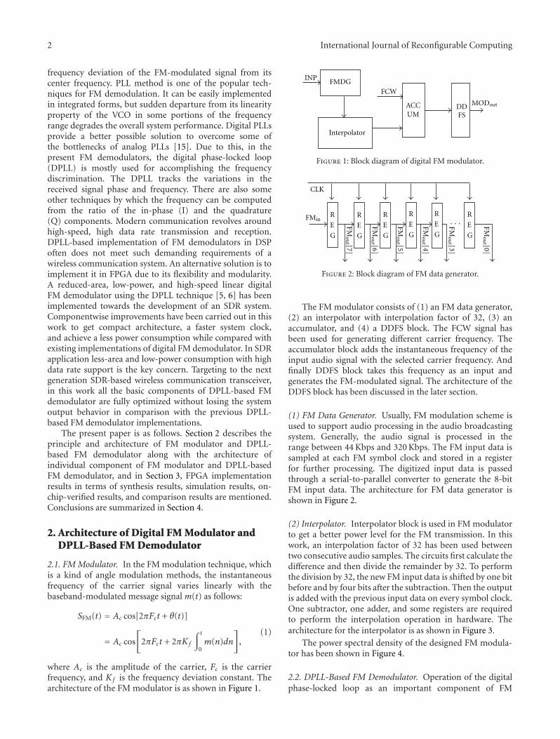
where Ac is the amplitude of the carrier, Fc is the carrierfrequency, and Kf is the frequency deviation constant. Thearchitecture of the FM modulator is as shown in Figure 1.
Interpolator
ACCUM
DDFS
FCW
INPFMDG
MODout
Figure 1: Block diagram of digital FM modulator.
R
E
G
R
E
G
R
E
G
R
E
G
R
E
G
R
E
G
CLK
· · ·FMin
FMou
t [0]
FMou
t [3]
FMou
t [4]
FMou
t [5]
FMou
t [6]
FMou
t [7]
Figure 2: Block diagram of FM data generator.
The FM modulator consists of (1) an FM data generator,(2) an interpolator with interpolation factor of 32, (3) anaccumulator, and (4) a DDFS block. The FCW signal hasbeen used for generating different carrier frequency. Theaccumulator block adds the instantaneous frequency of theinput audio signal with the selected carrier frequency. Andfinally DDFS block takes this frequency as an input andgenerates the FM-modulated signal. The architecture of theDDFS block has been discussed in the later section.
(1) FM Data Generator. Usually, FM modulation scheme isused to support audio processing in the audio broadcastingsystem. Generally, the audio signal is processed in therange between 44 Kbps and 320 Kbps. The FM input data issampled at each FM symbol clock and stored in a registerfor further processing. The digitized input data is passedthrough a serial-to-parallel converter to generate the 8-bitFM input data. The architecture for FM data generator isshown in Figure 2.
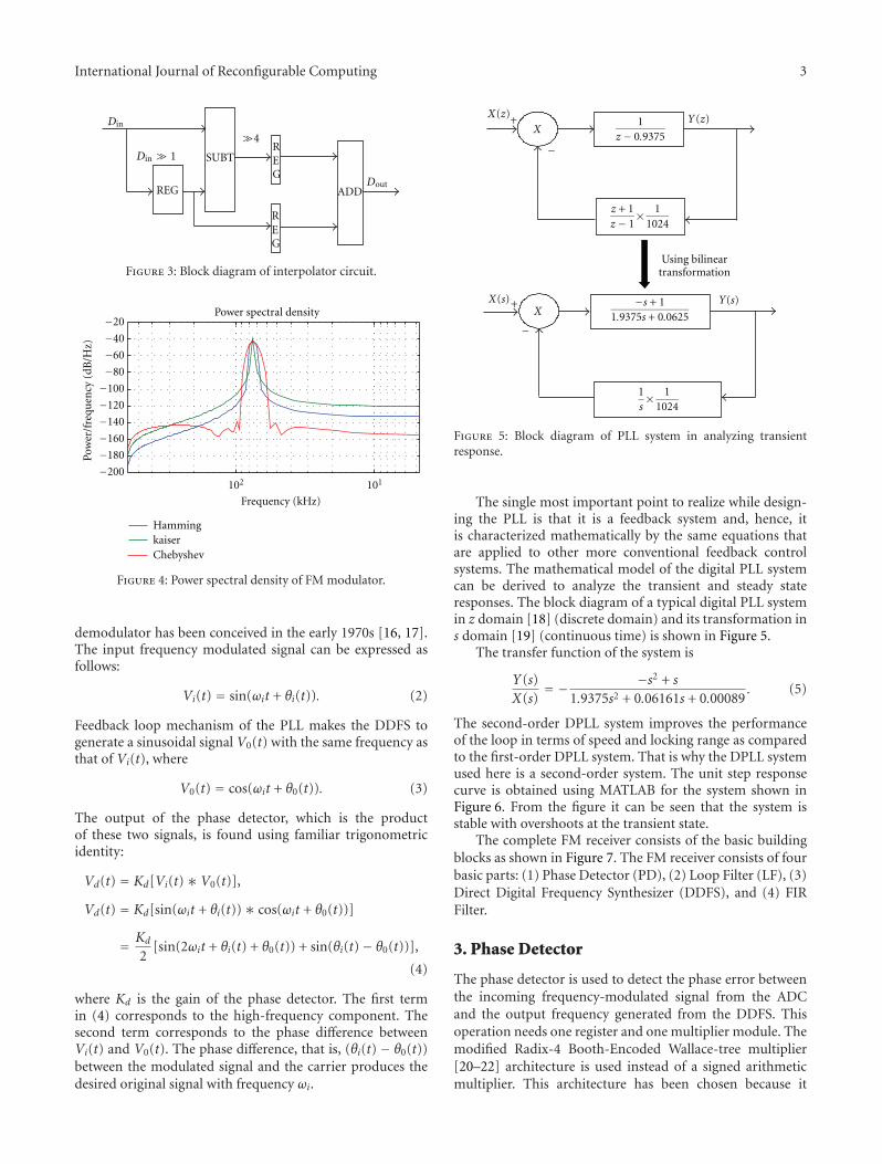
(2) Interpolator. Interpolator block is used in FM modulatorto get a better power level for the FM transmission. In thiswork, an interpolation factor of 32 has been used betweentwo consecutive audio samples. The circuits first calculate thedifference and then divide the remainder by 32. To performthe division by 32, the new FM input data is shifted by one bitbefore and by four bits after the subtraction. Then the outputis added with the previous input data on every symbol clock.One subtractor, one adder, and some registers are requiredto perform the interpolation operation in hardware. Thearchitecture for the interpolator is as shown in Figure 3.
The power spectral density of the designed FM modula-tor has been shown in Figure 4.
2.2. DPLL-Based FM Demodulator. Operation of the digitalphase-locked loop as an important component of FM
International Journal of Reconfigurable Computing 3
SUBT
REG ADD
REG
REG
Dout
Din
Din ≫ 1
≫4
Figure 3: Block diagram of interpolator circuit.
102 101−200
−180
−160
−140
−120
−100
−80
−60
−40
−20
Frequency (kHz)
Pow
er/f
requ
ency
(dB
/Hz)
Power spectral density
HammingkaiserChebyshev
Figure 4: Power spectral density of FM modulator.
demodulator has been conceived in the early 1970s [16, 17].The input frequency modulated signal can be expressed asfollows:
Vi(t) = sin(ωit + θi(t)). (2)
Feedback loop mechanism of the PLL makes the DDFS togenerate a sinusoidal signal V0(t) with the same frequency asthat of Vi(t), where
V0(t) = cos(ωit + θ0(t)). (3)
The output of the phase detector, which is the productof these two signals, is found using familiar trigonometricidentity:
Vd(t) = Kd[Vi(t)∗V0(t)],
Vd(t) = Kd[sin(ωit + θi(t))∗ cos(ωit + θ0(t))]
= Kd
2[sin(2ωit + θi(t) + θ0(t)) + sin(θi(t)− θ0(t))],
(4)
where Kd is the gain of the phase detector. The first termin (4) corresponds to the high-frequency component. Thesecond term corresponds to the phase difference betweenVi(t) and V0(t). The phase difference, that is, (θi(t) − θ0(t))between the modulated signal and the carrier produces thedesired original signal with frequency ωi.
1z − 0.9375
+
+
−
−
z + 1z − 1
× 11024
Using bilineartransformation
1s× 1
1024
−s + 11.9375s + 0.0625
Y(s)
X
X
X(z) Y(z)
X(s)
Figure 5: Block diagram of PLL system in analyzing transientresponse.
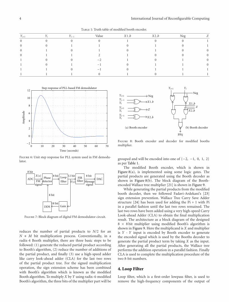
The single most important point to realize while design-ing the PLL is that it is a feedback system and, hence, itis characterized mathematically by the same equations thatare applied to other more conventional feedback controlsystems. The mathematical model of the digital PLL systemcan be derived to analyze the transient and steady stateresponses. The block diagram of a typical digital PLL systemin z domain [18] (discrete domain) and its transformation ins domain [19] (continuous time) is shown in Figure 5.
The transfer function of the system is
Y(s)X(s)
= − −s2 + s
1.9375s2 + 0.06161s + 0.00089. (5)
The second-order DPLL system improves the performanceof the loop in terms of speed and locking range as comparedto the first-order DPLL system. That is why the DPLL systemused here is a second-order system. The unit step responsecurve is obtained using MATLAB for the system shown inFigure 6. From the figure it can be seen that the system isstable with overshoots at the transient state.
The complete FM receiver consists of the basic buildingblocks as shown in Figure 7. The FM receiver consists of fourbasic parts: (1) Phase Detector (PD), (2) Loop Filter (LF), (3)Direct Digital Frequency Synthesizer (DDFS), and (4) FIRFilter.
3. Phase Detector
The phase detector is used to detect the phase error betweenthe incoming frequency-modulated signal from the ADCand the output frequency generated from the DDFS. Thisoperation needs one register and one multiplier module. Themodified Radix-4 Booth-Encoded Wallace-tree multiplier[20–22] architecture is used instead of a signed arithmeticmultiplier. This architecture has been chosen because it
4 International Journal of Reconfigurable Computing
Table 1: Truth table of modified booth encoder.
Yi+1 Yi Yi−1 Value X1 b X2 b Neg Z
0 0 0 0 1 0 0 1
0 0 1 1 0 1 0 1
0 1 0 1 0 1 0 0
0 1 1 2 1 0 0 0
1 0 0 −2 1 0 1 0
1 0 1 −1 0 1 1 0
1 1 0 −1 0 1 1 1
1 1 1 0 1 0 1 1
0 10 20 30 40 50 60 70−2
0
2
4
6
8
10
12
Time (seconds)
Am
plit
ude
Step response of PLL-based FM demodulator
Figure 6: Unit step response for PLL system used in FM demodu-lator.
ADCLoop FIR DAC
DDS
8 bit8 bit12 bit
18 bit
8 bit
FMsignal
Messagesignal
Phasedetector filter
Gain
8 bit
filterY(s)
X(s)
Figure 7: Block diagram of digital FM demodulator circuit.
reduces the number of partial products to N/2 for anN ∗ M bit multiplication process. Conventionally, in aradix-4 Booth multiplier, there are three basic steps to befollowed: (1) generate the reduced partial product accordingto Booth’s algorithm, (2) reduce the number of additions ofthe partial product, and finally (3) use a high-speed adderlike carry look-ahead adder (CLA) for the last two rowsof the partial product tree. For the signed multiplicationoperation, the sign extension scheme has been combinedwith Booth’s algorithm which is known as the modifiedBooth algorithm. To multiply X by Y using radix-4-modifiedBooth’s algorithm, the three bits of the multiplier part will be
Neg
(a) Booth encoder
Neg
PPij
(b) Booth decoder
Yi+1
Yi−1Yi
Yi+1 ZX2 bYi
Yi−1Yi
Yi+1 Yi
X2 b
Z
X1 bX1 b
Figure 8: Booth encoder and decoder for modified boothsmultiplier.
grouped and will be encoded into one of {−2, −1, 0, 1, 2}as per Table 1.
The modified Booth encoder, which is shown inFigure 8(a), is implemented using some logic gates. Thepartial products are generated using the Booth decoder asshown in Figure 8(b). The block diagram of the Booth-encoded Wallace tree multiplier [21] is shown in Figure 9.
While generating the partial products from the modifiedbooth decoder, then we followed Fadavi-Ardekani’s [23]sign extension prevention. Wallace Tree Carry Save Adderstructure [24] has been used for adding the Pi + 1 with Piin a parallel fashion until the last two rows remained. Thelast two rows have been added using a very high-speed CarryLook-ahead Adder (CLA) to obtain the final multiplicationresult. The architecture as a block diagram of the designed8 × 8 bit multiplier using modified Booth’s algorithm isshown in Figure 9. Here the multiplicand is X and multiplieris Y · Y input is encoded by Booth encoder to generatethe encoded signal which is used by the Booths decoder togenerate the partial product term by taking X as the input.After generating all the partial products, the Wallace treeperforms the addition operation in a parallel fashion. FinallyCLA is used to complete the multiplication procedure of thetwo 8-bit numbers.
4. Loop Filter
Loop filter, which is a first-order lowpass filter, is used toremove the high-frequency components of the output of

International Journal of Reconfigurable Computing 5
Partialproduct
generator
Wallacetree
Modified boothencoder/decoder
Singextension
8 bits
8 bits
16 bits
CLA
X
Y X ∗ Y
Figure 9: Block diagram of booth-encoded Wallace tree multiplier.
+
Gain(α)
8 bits
12 bits
Z−1
α = 1− 116
dtempPD OUT
LOOP OUT
Figure 10: Block diagram of first order loop filter.
the phase detector given by (4). Figure 10 shows the blockdiagram of the first-order loop filter used in the DPLL-basedFM demodulator system. The transfer function of the loopfilter is given by
H(z) = 1z − α
. (6)
Equation (6) can be implemented in hardware by theaddition of the output signal from the phase detector(PD OUT) and the register output multiplied by a coefficientα = (1− 1/16) = 15/16 = .09375, which is chosen to ensurethe system stability. Multiplication by a factor of 1/16 hasbeen implemented by 4-bit right shift instead of a multiplier.
5. Direct Digital Frequency Synthesizer
DDFS finds wide use as a component in modern com-munication system, radio detector, electronic warfare, highprecision measurement system, and high precision biomed-ical applications. DDFS accepts arbitrary frequency as itsreference frequency depending on the frequency controlword and generates one or more frequencies. The DDFSarchitecture was first given in [25]. The arithmetic operationsrequired to build a DDFS are a phase accumulator whichgenerates the phase for generating the cosine waveform anda phase to amplitude converter. Various researches have
been performed to design a high-performance circuit forphase-to-amplitude conversion as summarized in [26–28].The quarter-wave symmetry ROM technique is very usefulwhere a very low phase resolution has been used [29].Many ROM compression techniques have been proposed,but for low-resolution bit, these techniques are not suitableas they maximize the error. This DDFS has been designedfor waveform synthesis in DPLL-based FM demodulator. TheROM-based DDFS has been designed for use in the DPLL-based FM demodulator. In DPLL-based FM demodulator,the quadrature output from the DDFS is not required.Due to this fact, the ROM-based architecture (LUT) isconsidered to be superior to the CORDIC-based architecture[30] for the phase-to-amplitude conversion. To overcomethe disadvantages of ROM-based DDFS, namely, high-powerconsumption and low speed, a pipelined ROM-based DDFSapproach has been considered in the present work. Pipelinetechnique will help reduce the power consumption and alsomaximize the operating frequency. In the present work, thedesigned pipelined look-up table-based DDFS architecture isused as shown in Figure 11.
6. Fir Filter
The DDFS consists of a phase accumulator, a ROM look-up table, two 1’s complementers, a pipelined register, and anXOR gate. The designed DDFS has a free running frequencyof 1 MHz and requires 1024 sample values to define onecycle of a cosine signal. The DDFS generates the cosinesignal waveform by addressing the cosine ROM LUT at afrequency set by an 18-bit control word. If the referencesystem clock (Fclk) is set to 100 MHz, then the frequencyresolution will be 381.468 Hz. According to the accumulationrate in phase accumulator set by the FCW, the ROM producesthe cosine waveform at that programmed frequency. In thisimplementation, the frequency control word (FCW) and theoutput bits have been chosen to be 18 bits and 8 bits, whichprovides spurious free dynamic range (SFDR) of 64.3 dB. Asthe design is pipelined, the frequency switching will sufferfrom 2-clock cycle latency.
MATLAB 7.4.0 version is used for the performanceanalysis of the designed two DDFS blocks. The floatingpoint cosine wave generated using the MATLAB in-builtfunction and cosine wave generated by proposed pipelinedROM-based DDFS has been analyzed. The results areshown in Figure 12. Hence the FLTPNT COSINE is theMATLAB-generated cosine wave and FXDPOINT COSINEis the cosine wave generated by our proposed ROM-basedDDFS. The error between these two signals in the firstquadrant has been shown in Figure 13 (as quarter wavesymmetry property has been adopted). The minimum erroris −0.0088 and maximum error is 0.0089 which is nothingbut the quantization error (as 8 bits of amplitude has beenconsidered in proposed design).
At the last stage of the receiver, a lowpass Finite ImpulseResponse (FIR) filter is used to perform the signal shaping.Here a 16-tap transposed FIR filter architecture [31] is used,as shown in Figure 14. This filter is essentially an averaging
6 International Journal of Reconfigurable Computing
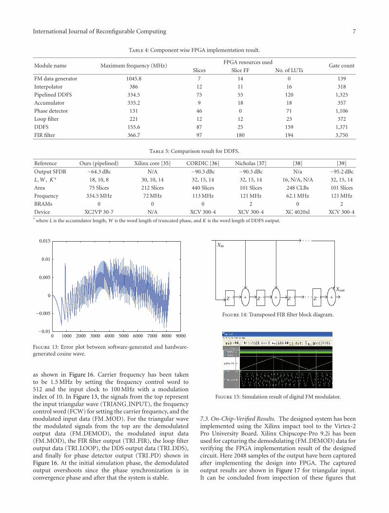
Table 2: Timing, Area, and Power results for 2vp30-7ff896.
AreaTiming (MHz) Power (mW)
No. of slice No. of FF No. of LUT Gate count
FM modulator 96 90 148 1,931 334.5 107.67
FM demodulator 233 240 436 6,400 131 108.67
REG
REG
Accumulator
Cosrom MUXMUX
nter
18 bit
Add IN
10 bit
8 bit
8 bit
8 bit
8 bit
8 bit
Quadrant selection
DDS
MSB1
MSB0
REG
OUT
LUT
Compleme-nterCompleme-
-
Figure 11: Block diagram of a pipelined ROM-based direct digital synthesizer.
0 0.5 1 1.5 2 2.5 3 3.5×10⁴
−1−0.8−0.6−0.4−0.2
00.20.40.60.8
1
No of sample
Cos
ine
valu
e
Fixed point ve floating point cosine wave plotrsus
.
Figure 12: Plot of software-generated versus hardware-generated(using proposed ROM-based DDFS) cosine wave.
filter since its output is equal to the average value of itsinput values over the last n-tap samples where n is thenumber of taps used. As in direct form digital FIR filterthe total propagation delay of the circuit increases moredue to the addition of the 16 data samples, a transposedFIR filter architecture is chosen [32–34] in the presentimplementation. Here the coefficients are the same 1/16, andin reality 1/16 can be implemented by just 4-bit right shiftoperation. Hence no multiplier is required.
7. FPGA Implementation Details
7.1. Synthesis Results. The proposed FM demodulator hasbeen described using the Verilog hardware description
Table 3: Detailed power analysis results for 2vp30-7ff896.
FM modulator FM demodulator
Clock power 1.72 mW 1.72 mW
Input power 0.73 mW 0.33 mW
Logic power 0.03 mW 1.83 mW
Output power 2.81 mW 11 mW
Signal power 0.04 mW 3.23 mW
Total power 107.67 mW 108.67 mW
language and Xilinx ISE 9.2i is used for synthesis andFPGA implementation. Xilinx XCV2vp30-7FF896 device hasbeen used as the target device for FPGA implementation,XST has been used as a synthesis tool, and XPower hasbeen used for power calculation. The power is beingcalculated by simulation-based switching activities of allthe signals. The synthesis results for the FM modulatorand demodulator have been listed in Table 2. Table 3 listedthe detailed dynamic power analysis result by applying a100 Mbps data rate to the FM modulator and demodu-lator. Table 4 shows the componentwise implementationreports.
7.2. Simulation Results. For the post place and route simu-lation in FPGA, the Modelsim-Xe 6.3c Starter version fromMentor Graphics is used as a logic simulator. The modulatedresponse of a 10 KHz triangular wave is shown in Figure 15.The demodulated response of the FM-modulated signal is
International Journal of Reconfigurable Computing 7
Table 4: Component wise FPGA implementation result.
Module name Maximum frequency (MHz)FPGA resources used
Gate countSlices Slice FF No. of LUTs
FM data generator 1045.8 7 14 0 139
Interpolator 386 12 11 16 318
Pipelined DDFS 334.5 75 55 120 1,325
Accumulator 335.2 9 18 18 357
Phase detector 131 46 0 71 1,106
Loop filter 221 12 12 23 372
DDFS 155.6 87 25 159 1,371
FIR filter 366.7 97 180 194 3,750
Table 5: Comparison result for DDFS.
Reference Ours (pipelined) Xilinx core [35] CORDIC [36] Nicholas [37] [38] [39]
Output SFDR −64.3 dBc N/A −90.3 dBc −90.3 dBc N/a −95.2 dBc
L,W , K∗ 18, 10, 8 30, 10, 14 32, 15, 14 32, 15, 14 16, N/A, N/A 32, 15, 14
Area 75 Slices 212 Slices 440 Slices 101 Slices 248 CLBs 101 Slices
Frequency 334.5 MHz 72 MHz 113 MHz 121 MHz 62.1 MHz 121 MHz
BRAMs 0 0 0 2 0 2
Device XC2VP 30-7 N/A XCV 300-4 XCV 300-4 XC 4020xl XCV 300-4∗
where L is the accumulator length, W is the word length of truncated phase, and K is the word length of DDFS output.
0 1000 2000 3000 4000 5000 6000 7000 8000 9000−0.01
−0.005
0
0.005
0.01
0.015
Figure 13: Error plot between software-generated and hardware-generated cosine wave.
as shown in Figure 16. Carrier frequency has been takento be 1.5 MHz by setting the frequency control word to512 and the input clock to 100 MHz with a modulationindex of 10. In Figure 13, the signals from the top representthe input triangular wave (TRIANG INPUT), the frequencycontrol word (FCW) for setting the carrier frequency, and themodulated input data (FM MOD). For the triangular wavethe modulated signals from the top are the demodulatedoutput data (FM DEMOD), the modulated input data(FM MOD), the FIR filter output (TRI FIR), the loop filteroutput data (TRI LOOP), the DDS output data (TRI DDS),and finally for phase detector output (TRI PD) shown inFigure 16. At the initial simulation phase, the demodulatedoutput overshoots since the phase synchronization is inconvergence phase and after that the system is stable.
Z−1 Z−1 Z−1 Z−1+ + +
· · ·
· · ·
Xin
Xout
Figure 14: Transposed FIR filter block diagram.
Figure 15: Simulation result of digital FM modulator.
7.3. On-Chip-Verified Results. The designed system has beenimplemented using the Xilinx impact tool to the Virtex-2Pro University Board. Xilinx Chipscope-Pro 9.2i has beenused for capturing the demodulating (FM DEMOD) data forverifying the FPGA implementation result of the designedcircuit. Here 2048 samples of the output have been capturedafter implementing the design into FPGA. The capturedoutput results are shown in Figure 17 for triangular input.It can be concluded from inspection of these figures that

8 International Journal of Reconfigurable Computing
Table 6: FPGA resource usage comparison result with other FM demodulators.
Architecture using Xilinx Spartan3 3S200FT256-4Time Area
Delay (ns) Frequency (MHz) Slices Slices FF LUT
PLL (optimized) [7] 9.725 102.828 491 548 721
Sigma Delta Arch. [11] 2427 out of 3071 slices in Xilinx Virtex2 XC2V500 device
Proposed implementation12.948 77.3 237 244 437
234 out of 3072 slices in Xilinx Virtex2 XC2V500 device
Table 7: Area utilization comparison with other FM demodulator implementations [5, 6].
Without optimization/no. of gate With optimization/no. of gate
Proposed design Existing architecture Proposed design Existing architecture
Phase detector: 389 Phase detector: 422 Phase detector: 413 Phase detector: 616
Loop filter: 202 Loop filter: 200 Loop filter: 277 Loop filter: 297
FIR filter: 3213 FIR filter: 2367 FIR filter: 3696 FIR filter: 3511
DDS/NCO: 608 DDS/NCO: 1534 DDS/NCO: 828 DDS/NCO: 1833
Total FM: 4844 Total FM: 10545 Total FM: 6052 Total FM: 14314
Table 8: Timing analysis comparison with other FM demodulator implementation [5, 6].
Without optimization With optimization
Proposed design Existing architecture Proposed design Existing architecture
Operating frequency 149.4 MHz Operating frequency 143.7 MHz Operating frequency 158.1 MHz Operating frequency 155.8 MHz
the designed circuit can effectively demodulate the FM inputsignal back to its original form.
7.4. Comparison Results. By optimizing the basic compo-nents of the FM demodulator, the reduction of the hardwareusage and improvement in the performance has been done.Table 5 has summarized the comparison result with otherROM compression techniques while implementing a directdigital synthesis. In this context, Table 6 shows the compari-son result with other existing FPGA implementations of FMdemodulator [7, 11].
The proposed circuit has been synthesized using theLeonardo Spectrum 2005b.24 Level 3 from Mentor Graphicsusing the TSMC 350 nm (typical) as a target technologylibrary. During the synthesis, speed has been considered asthe main constraint for the designed circuit. Another FMreceiver circuit has also been designed and synthesized usingthe Leonardo Spectrum 2004a.63 from Mentor Graphics andTSMC 350 nm (Fast) as a target technology library. FromTables 7 and 8, it is observed that the FM demodulatordesigned in this chapter is better in performance comparedto the available DPLL-based FM demodulator [5, 6].
8. Conclusions
A new high-performance digital FM modulator and adigital phase-locked loop-based FM demodulator have beenproposed in this paper. The FM modulator and demodulatorare designed to satisfy the constraint for the application inpersonal wireless communication and digital audio broad-casting. Individual componentwise optimization has made
Figure 16: Simulation result of FM demodulator for Triangularwave modulated input.
Figure 17: On-chip-verified result of the FM demodulator outputfor the triangular wave-modulated input.
the overall design superior than other implementations.FPGA implementation of the proposed design has beencarried out for quick prototyping of the digital FM modu-lator and demodulator chip. The simulation and synthesisresult of FM modulator shows that the digital up conversionis very much possible as it can achieve maximum clockfrequency of 334.5 MHz. From the on-chip-verified result it
International Journal of Reconfigurable Computing 9
can be clearly seen that the proposed FM demodulator candemodulate the signal back in its original form by consumingonly 6.4 K equivalent gate count. The comparison results forboth FPGA and ASIC implementations have shown that theproposed design is superior to the existing digital FM chips.Hence it is concluded that the designed high-performanceFM modulator and demodulator can be easily fitted intothe next generation software-defined radio-based handsetwhere low power and minimum hardware utilization withthe maximum clock frequency are desired features.
References
[1] S. Twelves and C. J. Kikkert, “Investigation into the effects ofquantisation noise on a digital FM modulator,” in Proceedingsof the IEEE TENCON Digital Signal Processing Applications(TENCON ’96), vol. 1, pp. 317–322, November 1996.
[2] J. Lahti and M. Niemisto, “A digital frequency modulatorcircuit for a dual-mode cellular telephone,” in Proceedingsof the IEEE International Symposium on Circuits and Systems(ISCAS ’98), pp. 405–408, June 1998.
[3] R. Unsikartano, J. Niittyahti, and M. Renfors, “Area-optimizedFPGA implementation of a digital FM modulator,” in Pro-ceedings of the IEEE International Symposium on Circuits andSystems (ISCAS ’99), vol. 4, pp. 360–362, July 1999.
[4] S. Twelves and C. J. Kikkert, “Performance of a digitalstereo FM modulator with reduced output resolution,” IEEETransactions on Broadcasting, vol. 43, no. 1, pp. 104–113, 1997.
[5] J. P. M. Brito and S. Bampi, “Design of a digital FM de-modulator based on a 2nd order all-digital phase-lockedloop,” in Proceedings of the 20th Symposium on IntegratedCircuits and System Design (SBCCI ’07), Session: Circuits forCommunications—Part 3, pp. 137–141, 2007.
[6] J. P. M. Brito and S. Bampi, “Design of a digital FM de-modulator based on a 2nd-order all-digital phase-lockedloop,” Analog Integrated Circuits and Signal Processing, vol. 57,no. 1-2, pp. 97–105, 2008.
[7] http://www.opencores.org/?do=project&who=simple fmreceiver.
[8] E. B. Ronald, Phase Locked Loop, Theory, Design, and Applica-tions, McGraw-Hill, New York, NY, USA, 2003.
[9] http://www.altera.com/literature/cp/fpga-cores-for-sdr.pdf.[10] C. Zhang, C. R. Anderson, and P. M. Athanas, “All digital
FPGA based FM radio receiver,” in Proceedings of the SDRForum Technical Conference, 2007.
[11] F. Yu, “FPGA implementation of a fully digital FM demodu-lator,” in Proceedings of the 9th IEEE Singapore InternationalConference on Communication Systems (ICCS ’04), pp. 446–450, September 2004.
[12] J. K. Holmes and C. R. Tegnelia, “A second-order all-digitalphase-locked loop,” IEEE Transactions on Communications,vol. 22, no. 1, pp. 62–68, 1974.
[13] B. S. Song and I. S. Lee, “Digital FM demodulator for FM,TV, and wireless,” IEEE Transactions on Circuits and Systems II:Analog and Digital Signal Processing, vol. 42, no. 12, pp. 821–825, 1995.
[14] N. Boutin, “An arctangent type wideband PM/FM demod-ulator with improved performance,” IEEE Transactions onConsumer Electronics, vol. 38, no. 1, pp. 5–9, 1992.
[15] G. Pasternack and R. L. Whalin, “Analysis and synthesis of adigital phase-locked loop for FM demodulation,” Bell SystemTechnical Journal, vol. 47, pp. 2207–2237, 1968.
[16] C. Kelly and S. Gupta, “The digital phase-locked loop asa near-optimum FM demodulator communications,” IEEETransactions Communications, vol. 20, no. 3, pp. 406–411,1972.
[17] D. R. Stephens, Phase-Locked Loops for Wireless Communi-cations Digital, Analog and Optical Implementations, KluwerAcademic Publishers, 2nd edition, 1998.
[18] J. G. Proakis and D. G. Manolakis, Digital Signal Proessing,Prentice Hall, Upper Saddle River, NJ, USA, 4th edition, 1996.
[19] K. Ogata, Modern Control Engineering, Prentice Hall, UpperSaddle River, NJ, USA, 3rd edition, 1997.
[20] K.-S. Cho, J.-O. Park, J.-S. Hong, and G.-S. Choi, “54×54-bit radix-4 multiplier based on modified booth algorithm,” inProceedings of the 13th ACM Great Lakes Symposium on VLSI,pp. 233–236, 2003.
[21] H. L. Lin, R. C. Chang, and M. T. Chan, “Design of a novelradix-4 Booth multiplier,” in Proceedings of the IEEE Asia-Pacific Conference on Circuits and Systems (APCCAS ’04), vol.2, pp. 837–840, December 2004.
[22] R. Hussin, A. Y. M. Shakaff, N. Idris, Z. Sauli, R. C. Ismail,and A. Kamarudin, “An efficient modified booth multiplierarchitecture,” in Proceedings of the International Conference onElectronic Design (ICED ’08), pp. 1–4, December 2008.
[23] J. Fadavi-Ardekani, “M × N booth encoded multiplier gener-ator using optimized Wallace trees,” IEEE Transactions on VeryLarge Scale Integration (VLSI) Systems, vol. 1, no. 2, pp. 164–167, 1993.
[24] S. Kumar, K. Forward, and M. Palaniswami, “A fast-multipliergenerator for FPGAs,” in Proceedings of the 8th InternationalConference on VLSI Design, pp. 53–56, January 1995.
[25] J. Tierney, C. Rader, and B. Gold, “A digital frequencysynthesizer,” IEEE Transaction on Audio and Electroacoustics,vol. 19, no. 1, pp. 48–57, 1971.
[26] D. A. Sunderland, R. A. Strauch, S. S. Wharfield, H. T.Peterson, and C. R. Cole, “CMOS/SOS frequency synthesizerLSI circuit for spread spectrum communications,” IEEEJournal of Solid-State Circuits, vol. 19, no. 4, pp. 497–506, 1984.
[27] H. T. Nicholas III and H. Samueli, “A 150-MHz directdigital frequency synthesizer in 1.25-μm CMOS with -90-dBcspurious performance,” IEEE Journal of Solid-State Circuits,vol. 26, no. 12, pp. 1959–1969, 1991.
[28] K. A. Essenwanger, V. S. Reinhardt, and A. Zarowin, “Sineoutput DDSs a survey of the state of the art,” in Proceedings ofthe IEEE International Frequency Control Symposium, pp. 370–378, May 1998.
[29] A. Bellaouar, M. S. O’brecht, A. M. Fahim, and M. I. Elmasry,“Low-power direct digital frequency synthesis for wirelesscommunications,” IEEE Journal of Solid-State Circuits, vol. 35,no. 3, pp. 385–390, 2000.
[30] S. Nahm, K. Han, and W. Sung, “A CORDIC-based digitalquadrature mixer: comparison with a ROM-based architec-ture,” in Proceedings of the IEEE International Symposium onCircuits and Systems (ISCAS ’98), vol. 4, pp. 385–388, June1998.
[31] A. T. Erdogan and T. Arslan, “Low power multiplicationscheme for FIR filter implementation on single multiplierCMOS DSP processors,” Electronics Letters, vol. 32, no. 21, pp.1959–1960, 1996.
[32] M. Mehendale, S. D. Sherlekar, and G. Venkatesh, “Techniquesfor low power realization of FIR filters,” in Proceedings of theAsia and South Pacific Design Automation Conference (ASP-DAC ’95), vol. 3, pp. 404–416, September 1995.
[33] “An introduction to digital filters,” an9603, Application note,Intersil, 1999.
10 International Journal of Reconfigurable Computing
[34] C. Nagendra, M. J. Irwin, and R. M. Owens, “Area-time-powertradeoffs in parallel adders,” IEEE Transactions on Circuits andSystems II: Analog and Digital Signal Processing, vol. 43, no. 10,pp. 689–702, 1996.
[35] Xilinx Core Generator System, http://www.xilinx.com/pro-ducts/intellectual-property/index.htm.
[36] J. Vankka, “Methods of mapping from phase to sine amplitudein direct digital synthesis,” in Proceedings of the 50th IEEEInternational Frequency Control Symposium, pp. 942–950, June1996.
[37] H. T. Nicholas and H. Samueli, “An analysis of output spec-trum of direct digital frequency synthesizers in the presenceof phase-accumulator truncation,” in Proceedings of the 41stAnnual Frequency Control Symposium,, pp. 495–502, 1987.
[38] F. Cardells-Tormo and J. Valls-Coquillat, “Optimized FPGA-implementation of quadrature DDS,” in Proceedings of theIEEE International Symposium on Circuits and Systems (ISCAS’02), pp. V/369–V/372, May 2002.
[39] M. Park, K. Kim, and J. A. Lee, “CORDIC-based directdigital frequency synthesizer: comparison with a ROM-basedarchitecture in FPGA implementation,” IEICE Transactions onFundamentals of Electronics, Communications and ComputerSciences, vol. 83, no. 6, pp. 1282–1285, 2000.

International Journal of
AerospaceEngineeringHindawi Publishing Corporationhttp://www.hindawi.com Volume 2010
RoboticsJournal of
Hindawi Publishing Corporationhttp://www.hindawi.com Volume 2014
Hindawi Publishing Corporationhttp://www.hindawi.com Volume 2014
Active and Passive Electronic Components
Control Scienceand Engineering
Journal of
Hindawi Publishing Corporationhttp://www.hindawi.com Volume 2014
International Journal of
RotatingMachinery
Hindawi Publishing Corporationhttp://www.hindawi.com Volume 2014
Hindawi Publishing Corporation http://www.hindawi.com
Journal ofEngineeringVolume 2014
Submit your manuscripts athttp://www.hindawi.com
VLSI Design
Hindawi Publishing Corporationhttp://www.hindawi.com Volume 2014
Hindawi Publishing Corporationhttp://www.hindawi.com Volume 2014
Shock and Vibration
Hindawi Publishing Corporationhttp://www.hindawi.com Volume 2014
Civil EngineeringAdvances in
Acoustics and VibrationAdvances in
Hindawi Publishing Corporationhttp://www.hindawi.com Volume 2014
Hindawi Publishing Corporationhttp://www.hindawi.com Volume 2014
Electrical and Computer Engineering
Journal of
Advances inOptoElectronics
Hindawi Publishing Corporation http://www.hindawi.com
Volume 2014
The Scientific World JournalHindawi Publishing Corporation http://www.hindawi.com Volume 2014
SensorsJournal of
Hindawi Publishing Corporationhttp://www.hindawi.com Volume 2014
Modelling & Simulation in EngineeringHindawi Publishing Corporation http://www.hindawi.com Volume 2014
Hindawi Publishing Corporationhttp://www.hindawi.com Volume 2014
Chemical EngineeringInternational Journal of Antennas and
Propagation
International Journal of
Hindawi Publishing Corporationhttp://www.hindawi.com Volume 2014
Hindawi Publishing Corporationhttp://www.hindawi.com Volume 2014
Navigation and Observation
International Journal of
Hindawi Publishing Corporationhttp://www.hindawi.com Volume 2014
DistributedSensor Networks
International Journal of