Embed Size (px)
Citation preview
Nanophotonics 2018; 7(1): 269–276
Research article Open Access
Frederik Wallaa, Matthias M. Wiechaa, Nicolas Mecklenbeck, Sabri Beldi, Fritz Keilmann, Mark D. Thomson and Hartmut G. Roskos*
Anisotropic excitation of surface plasmon polaritons on a metal film by a scattering-type scanning near-field microscope with a non-rotationally-symmetric probe tipDOI 10.1515/nanoph-2017-0042Received April 9, 2017; revised May 25, 2017; accepted May 25, 2017
Abstract: We investigated the excitation of surface plas-mon polaritons on gold films with the metallized probe tip of a scattering-type scanning near-field optical micro-scope (s-SNOM). The emission of the polaritons from the tip, illuminated by near-infrared laser radiation, was found to be anisotropic and not circularly symmetric as expected on the basis of literature data. We furthermore identified an additional excitation channel via light that was reflected off the tip and excited the plasmon polari-tons at the edge of the metal film. Our results, while obtained for a non-rotationally-symmetric type of probe tip and thus specific for this situation, indicate that when an s-SNOM is employed for the investigation of plasmonic structures, the unintentional excitation of surface waves and anisotropic surface wave propagation must be consid-ered in order to correctly interpret the signatures of plas-mon polariton generation and propagation.
Keywords: surface plasmon polaritons; surface waves; near-field microscopy; s-SNOM.
1 IntroductionA scattering-type scanning near-field optical microscope (s-SNOM) permits spectroscopy on surfaces from the visible to microwaves with a spatial resolution down to several tens of nanometers [1]. Based on an atomic-force microscope (AFM), the tip of the cantilever is illuminated with laser radiation, which is scattered at the apex of the tip to provide the near-field spectroscopic response. In the case of metallic tips, it was shown in the literature that the tip can also excite surface plasmon polaritons (SPPs) and surface phonon polaritons [2–6].
SPPs on conductive surfaces have usually been excited by illumination of edges, trenches, and other surface disruptions with electromagnetic radiation, which has a component of the electrical radiation field perpendicular to the respective boundary [7–10]. The polaritons can be detected by a variety of techniques, among them holographic recording [11], observation of SPP-induced stray light with a camera [7], two-photon photo-emission electron microscopy [8, 12], and SNOM [9, 10]. Recently, the s-SNOM technique [1, 13, 14] was also employed, in this case to investigate SPPs on a gold film with a nano-trench etched into it. A beam of visible laser radiation both excited SPPs at the trench and illu-minated the s-SNOM tip, leading to the observation of signal modulation fringes due to the coherent interfer-ence between the SPPs and the probe light [2]. Our exper-iments follow the same route with the exception that we replace the nano-trench with a 10 × 10 μm2 square hole, which allows us to simultaneously explore SPP edge
aFrederik Walla and Matthias M. Wiecha: These authors contributed equally to this work.*Corresponding author: Hartmut G. Roskos, Physikalisches Institut, Johann Wolfgang Goethe-Universität, Max-von-Laue-Strasse 1, 60438 Frankfurt am Main, Germany, e-mail: [email protected]. http://orcid.org/0000-0003-3980-0964Frederik Walla: Department of Electronics Technology, Universidad Carlos III de Madrid, Leganes, Madrid 28911, SpainMatthias M. Wiecha, Nicolas Mecklenbeck and Mark D. Thomson: Physikalisches Institut, Johann Wolfgang Goethe-Universität, Max-von-Laue-Strasse 1, 60438 Frankfurt am Main, GermanySabri Beldi: Centre de Recherche en Microélectronique et Nanotechnologie, Technopôle de Sousse, Sahloul, TunisiaFritz Keilmann: Soft Condensed Matter Group and Center for NanoScience, Ludwig-Maximilians-Universität, Geschwister-Scholl-Platz 1, D-80539 München, Germany
©2017, Hartmut G. Roskos et al., published by De Gruyter. This work is licensed under the Creative Commons Attribution-NonCommercial-NoDerivatives 3.0 License. Unangemeldet
Heruntergeladen am | 25.10.19 11:14

270 F. Walla et al.: Anisotropic excitation of surface plasmon polaritons
generation with four different relative orientations of the tip, edge, and incoming beam. As will be shown, these results expose a clear signature for additional SPP excitation channels associated with the influence of the s-SNOM tip.
That the tip – at least if it is metallic or coated with a metal – can also generate surface waves became promi-nently known by experiments in the infrared spectral range on plasmons on graphene, reported by Fei et al. [3]. Even before that publication, Chang et al. [4] described s-SNOM measurements in the visible spectral range (wave-length: 532 nm) devoted to the study of SPPs on patterned silver, which can only be interpreted in the way that the tip contributed to SPP excitation. Later, other types of surface waves were also generated in that way, e.g. surface phonon polaritons on boron nitride [5, 6]. A striking feature of the standing-wave images reproduced in these papers is that they all point toward an isotropic excitation of the surface waves by the tips. The surprising aspect is that neither the illumination of the tips nor their shapes were rotationally symmetric. The isotropic generation can be illustrated, for example, on the basis of the data of Figure 1d of Ref. [3], which displays the same standing-wave pattern all around an imperfection of the graphene film studied. Such images are recorded with a fixed direction of the illumination and a fixed orientation of the cantilever. An anisotropic, at least partially directed excitation of surface waves by the tip would have led to a variation of the intensity of the stand-ing-wave pattern around the imperfection. Rotationally symmetric generation implies that the enhanced electric field at the apex of the tip is the source of the excited SPP, the strong localization of the field under the tip making the excitation process essentially isotropic.
Contrasting these findings, we present data for the case of SPP excitation on gold in the visible spectral range, which demonstrate preferentially directed SPP generation by the probe tip. While our observations have been made with one type of commercially available probe tips (for another commonly used one, see Supplemental B), the data show that SPP generation by the probe tip is by no means universally isotropic as one may assume based on such literature reports as those mentioned above.
2 Experimental detailsThe s-SNOM apparatus employed here is a refurbished system whose original version was built at the Max-Planck-Institut für Biochemie, Martinsried, Germany, and used
for the experiments reported in Refs. [15, 16], as well as for the first demonstration of a time-domain THz s-SNOM [17]. A scheme of the set-up is shown in Figure 1A. The AFM employs a laser diode (wavelength: 635 nm) and a position-sensitive detector for sample-tip distance control (with a typical cantilever oscillation frequency of Ω/2π ~120 kHz). The control electronics and data acquisition are based on software/hardware from Anfatec Instruments AG (Oelsnitz, Germany). The AFM probe tips are fully plat-inum-coated commercial tips HQ:NSC14/pt, Mikromasch, NanoAndMore (Watsonville, CA, USA) made from single-crystalline Si (cantilever and tip). The sample consists of a 100-nm-thick film of Au on 5 nm of Cr deposited by thermal respective e-beam evaporation onto an ITO-on-fused-silica substrate (ITO: indium tin oxide). The square window in the gold film is realized by optical lithography prior to Au/Cr deposition and subsequent lift-off process-ing. The window contains either the bare ITO layer (in the case of the measurements shown in Supplemental B) or an array of nano-rings (image in Figure 1B). Surface waves on the sample are excited and probed by illumination of the tip and its vicinity with 1.5–2 mW of power from a continuous-wave laser (LION, Sacher Lasertechnik GmbH, Marburg, Germany) operating at a wavelength of 850 nm. The light is focused onto the probe tip with a paraboloi-dal mirror with a focal length of 10 mm. The p-polarized light (i.e. polarized in the plane of incidence and hence with maximal projection along the tip) impinges roughly at an angle of 60° relative to the surface normal along the axis of the cantilever. The focal spot size of the radiation is 4–5 μm. The spot remains fixed in position relative to the tip, while the sample underneath is scanned by an XY-piezo-flexure stage. The scattered light from the tip is detected retroreflected along the same axis as the incom-ing beam. A beam splitter is used to separate a fraction of the scattered light toward an Si photodiode, whose signal is demodulated at either 2Ω or 3Ω. Both signal harmonics result in a similar resolution and modulation depth for the observed SPP interference fringes.
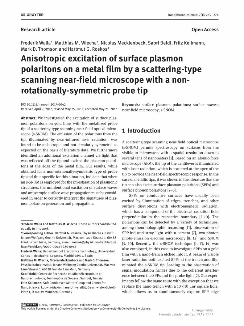
3 Experimental results and analysisFigure 1B displays a raster image of the scattered radia-tion signal, upon lateral translation of the sample under the illuminated tip, where the moderately focused, inci-dent laser beam is indicated by the blue arrow .k
We
observe periodic spatial signal modulations at all four edges (labeled 1–4), with the intensity peaks and valleys running parallel to the edges. One observes an addi-tional modulation – most clearly visible in regions 2 and
UnangemeldetHeruntergeladen am | 25.10.19 11:14
F. Walla et al.: Anisotropic excitation of surface plasmon polaritons 271
AFMLaser
Lock-inAmplifier
6
0 1 2 3 4 5–90
15
10
5
Edge
K (
µm–1
)
0
1
24
3
90
Fit (Eq. 2)
Exp.
φ (°)
φ1 = –80.3°, θ = 59.4°
180 270
450
600
750
1000
Λ (
nm)
2000
6000
β
θ
φkk||
k y
z E
Au
x
kSPP
4
8
12
16
20
Profile 4
Profile 2
Profile 1
6
8
10
Profile 3
x (µm)
7
8
9
10
8
10
12
14
Detector
2
3
0
3
6
9
12
s-S
NO
M s
igna
l (2Ω
)
15
18
21 µV
2 µm
M1
M2
A B
C D
E
ε
PSD
y 1
x1k
1
ITOsubstrate
4
s-SN
OM
Laser
L1
BS
λ/2
Au filmAu film
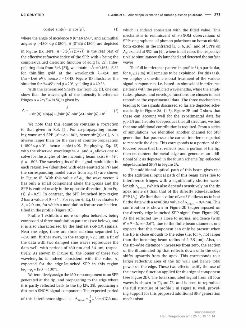
Figure 1: s-SNOM set-up and measurements at a square hole in a gold film on ITO substrate.(A) Set-up with PSD: position-sensitive detector; L1: lens for the position-sensing laser light; M2: paraboloidal mirror with a focal length of 10 mm; λ/2: half-wave plate for the control of the polarization of the light impinging onto the probe tip; BS: beam-splitter for out-coupling of the laser radiation returning from the probe tip. (B) Raster-scan image of the s-SNOM signal taken by translation of the sample under the illuminated tip, which is kept at a fixed position (signal demodulated at 2Ω). The red frame indicates the square hole in the gold film, with its boundaries being determined by simultaneous AFM topography recording (not shown). Also included are the x- and y-axis for region 1. The reduced signal strength in the lower part of the image is the result of a surface contamination picked up by the tip during a line scan in the middle of the scanned area. (C) s-SNOM signal profiles extracted along the white lines in B for each region 1–4 vs. distance y from their corresponding edges. The positions of the lines are chosen such that disturbances by defects on the surface are avoided. Note that the spatial decay lengths of the signal modulation do not represent that of the SPPs alone, as they are excited by the incoming beam that stays fixed to the tip while the sample is scanned. The dotted fit curves yield the oscillation periods mentioned in the text. (D) Schematic wave vectors and angles appearing in Eqs. (1) and (2).
k and
SPPk denote the wave vectors of the incoming beam and the SPP launched at the
edge, respectively, while = −
SPPK k k denotes the expected wave vector of the observed s-SNOM interference signals. (E) Wavelengths Λ of
the SPP interference fringes vs. respective azimuthal angle φ and model curve using Eq. (2).
UnangemeldetHeruntergeladen am | 25.10.19 11:14
272 F. Walla et al.: Anisotropic excitation of surface plasmon polaritons
4 – which is parallel to the wave front of the incoming laser radiation. This is a measurement artifact discussed in Supplemental C in connection with Supplemental Figure 3 shown there. The modulations inside the Au window are modes of the nano-ring meta-material not addressed further here.
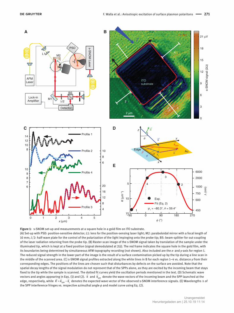
The signal profiles along the lines in Figure 1B are dis-played in Figure 1C. Along line 1, the signal corresponds to a damped sine wave (superposed on a constant offset) with a spatial period of Λ1 = 460 nm; similarly along line 2, only with a period of Λ2 = 1200 nm. Along line 3, i.e. in the down-stream direction with respect to the incoming laser beam, the signal is more complex, as discussed below in connection with Figure 2. Note that these features were reproduced with many other samples, both in the 2Ω- and 3Ω-demodulated signals (see examples in Supplemental Figure 2).
In the following, we focus on the identification of the origin of the spatial modulations. They arise from the inter-ference of waves – SPPs and free-space radiation – which need to be determined. Characteristic features help us narrow down the options and avoid consideration of all reflected/scattered waves reaching the photodiode (for theoretical aspects of a full-wave approach, especially also for the application of the reciprocity theory, see Refs. [18–21]; for a consideration of the role of light that is scattered
at the edges but does not convert to SPPs, see comments in Supplemental D). The modulations must arise from SPPs generated at or reflected from the edges to form intensity peaks/valleys parallel to them. They propagate to the tip and interfere there with the incoming radiation. As we will see, we need SPPs generated in different ways to fully explain the modulations that we have set out to identify.
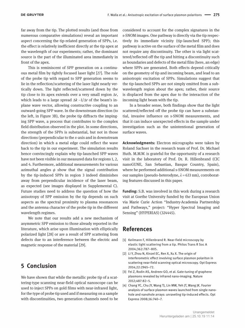
A first scenario involves the directly edge-excited SPPs, schematically shown in Figure 2A, sketch 2, which interfere at the probe tip with the incident light wave (see sketch 1 in Figure 2A). The light wave and the SPP arrive at the probe tip with wave vectors k
and SPP ,k
respectively,
resulting in a spatial modulation of the total s-SNOM intensity with wave vector SPPK k k= −
(where k
is the
projection of k in the surface plane; see Figure 1D). Note
that while the focused incoming beam is indeed composed of a distribution of wave vectors (with a full cone angle of Δθ ~ 12° for the beam used here), we assume that the total interaction averages essentially to that of a quasi-plane wave where k
is along the beam axis. The SPP propa-
gation direction SPPk
is dictated by the phase-matching condition along the edge, i.e. kSPP,x = kx, which results in interference fringes that are always parallel to the respec-tive edge [2] (as Kx = 0), and corresponds to a generalized Snell’s (Ibn Sahl’s) law:
All four waves
AB
C
D
E
k
kn
k
1. Incomingwave
k
z
x y
θ
α α
α α
θ
θ′
2. Edge-launchedSPP
kSPP
3. Tip-launchedSPP
4. Tip-reflectededge-launched SPP
0 1 2 3 4
Distance from edge y3 (µm)
5 6
2
1
0
2
1
2
1
2
1
kSPP kSPP
Sca
ttere
d si
gnal
(ar
b. u
.)
(1) + (2)+ tip-reflected
edge-launched SPP (4)
(1) + (2)+ tip-launched SPP (3)
Incoming wave (1)+ edge-launched SPP (2)
Figure 2: Numerical simulation of the s-SNOM signal along line 3 in Figure 1.(A) Sketch of four coherent s-SNOM signal contributions: (1) incoming beam; (2) SPP generated at the metal edge; (3) SPP launched at the s-SNOM tip, propagating to the edge of the metal film, reflected there and returning to the tip; (4) incoming beam reflected from the tip shaft onto the metal edge, generating an SPP there that propagates to the tip. (B–E) Calculated s-SNOM signals (time-averaged absolute square of the sum of the fields) at the location of the tip a distance y3 from the metal edge for various combinations of the four signal contributions in A. In D and E, the tip-reflected edge-launched SPP contribution (4) is modeled with an envelope that initially grows from y3 = 0 and then decays to zero for y3 > 1.8 μm (dashed line in D), as discussed in the text.
UnangemeldetHeruntergeladen am | 25.10.19 11:14
F. Walla et al.: Anisotropic excitation of surface plasmon polaritons 273
cos( ) sin( ) cos( ),nφ θ β⋅ = ⋅ (1)
where the angle of incidence θ (0° ≤ θ ≤ 90°) and azimuthal angles φ (−180° < φ ≤ 180°), β (0° ≤ β ≤ 180°) are depicted
in Figure 1D. Here, ( /(1 ))n = ℜ +ε ε is the real part of the effective refractive index of the SPP, with ε being the complex-valued dielectric function of gold [9, 22]. Inter-polating data from Ref. [23], we obtain 0.165 i5.32= +ε for thin-film gold at the wavelength l = 850 nm (ħω = 1.46 eV), hence n = 1.018. Figure 1D illustrates the situation for θ = 45° and φ = 20°, yielding β = 49.3°.
With the generalized Snell’s law from Eq. (1), one can show that the wavelength of the intensity interference fringes Λ = 2π/K = 2π/Ky is given by
2 2 2 2
.sin( ) sin( ) sin ( ) sin ( ) sin ( ) n
λΛ
θ φ θ φ θ=
− ⋅ + ⋅ − + (2)
We note that this equation contains a correction to that given in Ref. [2]. For co-propagating incom-ing wave and SPP [0° ≤ φ ≤ 180°, hence sin(φ) ≥ 0], Λ is always larger than for the case of counter-propagation (−180° < φ < 0°, hence sin(φ) < 0). Employing Eq. (2) with the observed wavelengths Λ1 and Λ2 allows one to solve for the angles of the incoming beam axis: θ = 59°, φ1 = − 80°. The wavelengths of the signal modulation in each region 1–4 (identified with edge-emitted SPPs) and the corresponding model curve from Eq. (2) are shown in Figure 1E. With this value of φ1, the wave vector k
has only a small component along the x1-axis and the SPP is emitted nearly in the opposite direction [from Eq. (1), β = 82°]. In contrast, the SPP launched into region 2 has a value of β = 34°. For region 4, Eq. (2) evaluates to Λ4 = 2.0 μm, for which a modulation feature can be iden-tified in the profile (Figure 1C).
Profile 3 exhibits a more complex behavior, being composed of three modulation patterns (see below), and it is also characterized by the highest s-SNOM signals. Near the edge, there are three maxima separated by ≈650 nm; further away, in the range y3 > 2.5 μm, a fit of the data with two damped sine waves reproduces the data well, with periods of 430 nm and 5.4 μm, respec-tively. As shown in Figure 1E, the longer of these two wavelengths is indeed consistent with the value Λ3 expected for the edge-launched SPP in this region (φ3 = φ1 + 180° = 100°).
We tentatively assign the 430-nm component to an SPP generated at the tip, and propagating to the edge where it is partly reflected back to the tip [24, 25], producing a distinct s-SNOM signal component. The expected period
of this interference signal is SPP,tip1 / 417.4 nm,2
nΛ λ= =
which is indeed consistent with the fitted value. This mechanism is reminiscent of s-SNOM observations of SPPs on graphene, of phonon polaritons on boron nitride, both excited in the infrared [3, 5, 6, 26], and of SPPs on Ag excited at 532 nm [4], where in all cases the respective tip also simultaneously launched and detected the surface waves.
The full interference pattern in profile 3 (in particular, for y3 2 μm) still remains to be explained. For this task, we employ a one-dimensional treatment of the various signal components, i.e. based on sinusoidal interference patterns with the predicted wavelengths, while the ampli-tudes, phases, and envelope functions are chosen to best reproduce the experimental data. The three mechanisms leading to the signals discussed so far are depicted sche-matically in Figure 2A, (1–3). Figure 2B and C show that these can account well for the experimental data for y3 > 2.5 μm. In order to reproduce the full structure, we find that one additional contribution is required. From a series of simulations, we identified another channel for SPP generation that possesses the correct interference period to reconcile the data. This corresponds to a portion of the focused beam that first reflects from a portion of the tip, then encounters the metal edge and generates an addi-tional SPP, as depicted in the fourth scheme (tip-reflected edge-launched SPP) in Figure 2A.
The additional optical path of this beam gives rise to the additional optical path of this beam gives rise to interference fringes with a significantly shorter wave-length ΛSPP,refl (which also depends sensitively on the tip apex angle α) than that of the directly edge-launched SPP (Λ3). We find that a value of α = 31° allows us to best fit the data with a resulting value of ΛSPP,refl = 874 nm. This contribution is shown in Figure 2D (superimposed on the directly edge-launched SPP signal from Figure 2B). As the reflected ray is close to normal incidence (with θ′ = θ − 2α = − 2.6°), due to the finite beam diameter, one expects that this component can only be present when the tip is close enough to the edge (i.e. for y3 not larger than the incoming beam radius of 2–2.5 μm). Also, as the tip-edge distance y increases from zero, the section of the illuminated tip that reflects down onto the edge shifts upwards from the apex. This corresponds to a larger reflecting area of the tip wall and hence total power on the edge. These two effects justify the use of the envelope function applied for this signal component (see Figure 2D). The total simulated signal from all four waves is shown in Figure 2E, and is seen to reproduce the full structure of profile 3 in Figure 1C well, provid-ing support for this proposed additional SPP generation mechanism.
UnangemeldetHeruntergeladen am | 25.10.19 11:14
274 F. Walla et al.: Anisotropic excitation of surface plasmon polaritons
4 Anisotropy – full-wave simulations
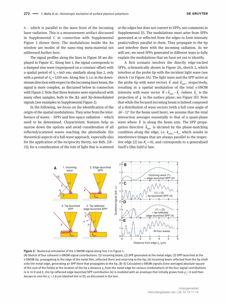
Returning now to a discussion of the tip-launched SPP contribution identified in region 3, the question arises as to why such an SPP is not also observed in regions 1, 2, and 4. One could expect SPP emission from the tip’s apex to occur with (near-)circular symmetry, in which case it should also be observable there (with the same interfer-ence wavelength ΛSPP,tip). In order to investigate the role of the tip further [16], we performed simulations of SPP generation by the tip on a planar gold surface with the Maxwell solver CST Microwave Studio from CST – Com-puter Simulation Technology AG (Darmstadt, Germany).
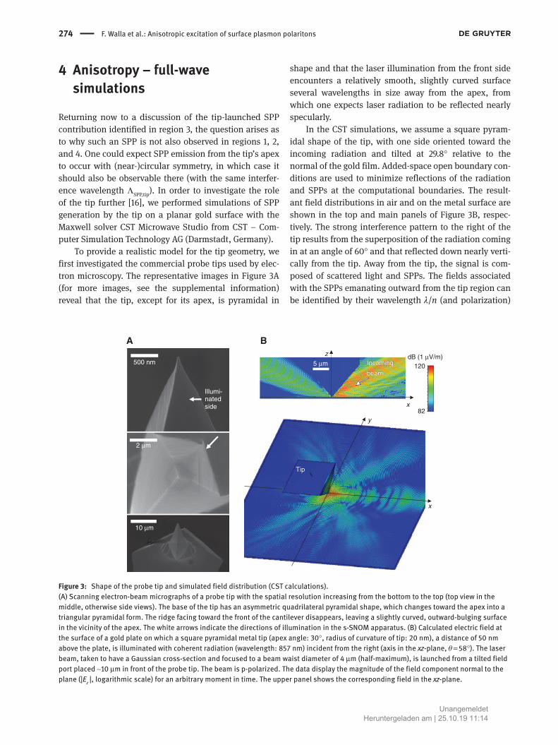
To provide a realistic model for the tip geometry, we first investigated the commercial probe tips used by elec-tron microscopy. The representative images in Figure 3A (for more images, see the supplemental information) reveal that the tip, except for its apex, is pyramidal in
shape and that the laser illumination from the front side encounters a relatively smooth, slightly curved surface several wavelengths in size away from the apex, from which one expects laser radiation to be reflected nearly specularly.
In the CST simulations, we assume a square pyram-idal shape of the tip, with one side oriented toward the incoming radiation and tilted at 29.8° relative to the normal of the gold film. Added-space open boundary con-ditions are used to minimize reflections of the radiation and SPPs at the computational boundaries. The result-ant field distributions in air and on the metal surface are shown in the top and main panels of Figure 3B, respec-tively. The strong interference pattern to the right of the tip results from the superposition of the radiation coming in at an angle of 60° and that reflected down nearly verti-cally from the tip. Away from the tip, the signal is com-posed of scattered light and SPPs. The fields associated with the SPPs emanating outward from the tip region can be identified by their wavelength λ/n (and polarization)
10 µm
2 µm
500 nmz
A B
x
x
y
dB (1 µV/m)
82
120
Tip
5 µm
Illumi-natedside
Incoming
beam
Figure 3: Shape of the probe tip and simulated field distribution (CST calculations).(A) Scanning electron-beam micrographs of a probe tip with the spatial resolution increasing from the bottom to the top (top view in the middle, otherwise side views). The base of the tip has an asymmetric quadrilateral pyramidal shape, which changes toward the apex into a triangular pyramidal form. The ridge facing toward the front of the cantilever disappears, leaving a slightly curved, outward-bulging surface in the vicinity of the apex. The white arrows indicate the directions of illumination in the s-SNOM apparatus. (B) Calculated electric field at the surface of a gold plate on which a square pyramidal metal tip (apex angle: 30°, radius of curvature of tip: 20 nm), a distance of 50 nm above the plate, is illuminated with coherent radiation (wavelength: 857 nm) incident from the right (axis in the xz-plane, θ = 58°). The laser beam, taken to have a Gaussian cross-section and focused to a beam waist diameter of 4 μm (half-maximum), is launched from a tilted field port placed ~10 μm in front of the probe tip. The beam is p-polarized. The data display the magnitude of the field component normal to the plane (|Ez |, logarithmic scale) for an arbitrary moment in time. The upper panel shows the corresponding field in the xz-plane.
UnangemeldetHeruntergeladen am | 25.10.19 11:14
F. Walla et al.: Anisotropic excitation of surface plasmon polaritons 275
far away from the tip. The plotted results (and those from numerous comparative simulations) reveal an important aspect concerning the tip-related generation of SPPs, i.e. the effect is relatively inefficient directly at the tip apex at the wavelength of our experiments; rather, the dominant source is the part of the illuminated area immediately in front of the apex.
This is reminiscent of SPP generation on a continu-ous metal film by tightly focused laser light [27]. The role of the probe tip with regard to SPP generation seems to lie in the reflection/scattering of the laser light nearly ver-tically down. The light reflected/scattered down by the tip close to its apex extends over a very small region Δr, which leads to a large spread Δk ~1/Δr of the beam’s in-plane wave vector, allowing constructive coupling to an outward-going SPP wave. In the downstream direction (to the left, in Figure 3B), the probe tip diffracts the imping-ing SPP wave, a process that contributes to the complex field distribution observed in the plot. In some directions, the strength of the SPPs is substantial, but not in those directions (perpendicular to the x-axis and in downstream direction) in which a metal edge could reflect the wave back to the tip in our experiment. The simulation results hence convincingly explain why tip-launched SPP waves have not been visible in our measured data for regions 1, 2, and 4. Furthermore, additional measurements for various azimuthal angles φ show that the signal contribution by the tip-induced SPPs in region 3 indeed diminishes away from perpendicular incidence of the laser beam, as expected (see images displayed in Supplemental C). Future studies need to address the question of how the anisotropy of SPP emission by the tip depends on such aspects as the spectral proximity to plasma resonances and the antenna character of the probe tip in the different wavelength regimes.
We note that our results add a new mechanism of asymmetric SPP emission to those already reported in the literature, which arise upon illumination with elliptically polarized light [28] or are a result of SPP scattering from defects due to an interference between the electric and magnetic response of the material [29].
5 ConclusionWe have shown that while the metallic probe tip of a scat-tering-type scanning near-field optical nanoscope can be used to inject SPPs on gold films with near-infrared light, for the type of probe tip used and if measuring on a sample with discontinuities, two generation channels need to be
considered to account for the complex signatures in the s-SNOM images. One pathway is directly via the tip respec-tively its immediate vicinity (tip-launched SPP); this pathway is active on the surface of the metal film and does not require any discontinuity. The other is via light scat-tered/reflected off the tip and hitting a discontinuity such as boundaries and defects of the metal film (here, an edge) where SPPs are generated. Both effects depend critically on the geometry of tip and incoming beam, and lead to an anisotropic excitation of SPPs. Simulations suggest that the tip-launched SPPs are not simply emitted from a sub-wavelength region about the apex; rather, their source is displaced from the apex due to the interaction of the incoming light beam with the tip.
In a broader sense, both findings show that the light scattered/reflected off the probe tip can have a substan-tial, invasive influence on s-SNOM measurements, and that it can induce unexpected effects in the sample under investigation such as the unintentional generation of surface waves.
Acknowledgments: Electron micrographs were taken by Roland Sachser in the research team of Prof. Dr. Michael Huth. M.M.W. is grateful for the opportunity of a research visit in the laboratory of Prof. Dr. R. Hillenbrand (CIC nanoGUNE, San Sebastian, Basque Country, Spain), where he performed additional s-SNOM measurements on our samples (pseudo-heterodyne, λ = 633 nm), corroborat-ing features discussed in this paper.
Funding: S.B. was involved in this work during a research visit at Goethe University funded by the European Union via Marie Curie Action “Industry-Academia Partnership and Pathways,” project: “Hyper Spectral Imaging and Sensing” (HYPERIAS) (324445).
References[1] Keilmann F, Hillenbrand R. Near-field microscopy by
elastic light scattering from a tip. Philos Trans R Soc A 2004;362:787–805.
[2] Li Y, Zhou N, Kinzel EC, Ren X, Xu X. The origin of interferometric effect involving surface plasmon polariton in scattering near-field scanning optical microscopy. Opt Express 2014;22:2965–72.
[3] Fei Z, Rodin AS, Andreev GO, et al. Gate-tuning of graphene plasmons revealed by infrared nano-imaging. Nature 2012;487:82–5.
[4] Chang YC, Chu JY, Wang TJ, Lin MW, Yeh JT, Wang JK. Fourier analysis of surface plasmon waves launched from single nano-hole and nanohole arrays: unraveling tip-induced effects. Opt Express 2008;16:740–7.
UnangemeldetHeruntergeladen am | 25.10.19 11:14

276 F. Walla et al.: Anisotropic excitation of surface plasmon polaritons
[5] Dai S, Fei Z, Ma Q, et al. Tunable phonon polaritons in atomi-cally thin van der Waals crystals of boron nitride. Science 2014;343:1125–9.
[6] Dai S, Ma Q, Yang Y, et al. Relative efficiency of polariton emis-sion in two-dimensional materials. Cond Mat arXiv:1704.05618.
[7] Lamprecht B, Krenn JR, Schider G, et al. Surface plasmon propagation in microscale metal stripes. Appl Phys Lett 2001;79:51–3.
[8] Zhang L, Kubo A, Wang L, Petek H, Seideman T. Imaging of surface plasmon polariton fields excited at a nanometer-scale slit. Phys Rev B 2011;84:245442.
[9] Salomon L, Basou G, Aourag H, et al. Local excitation of surface plasmon polaritons at discontinuities of a metal film: theoreti-cal analysis and optical near-field measurements. Phys Rev B 2002;65:125409.
[10] Aigouy L, Lalanne P, Hugonin JP, Julié G, Mathet V, Mortier M. Near-field analysis of surface waves launched at nanoslit aper-tures. Phys Rev Lett 2007;98:153902.
[11] Keilmann F, Kussmaul KW, Szentirmay Z. Imaging of optical wavetrains. Appl Phys B 1988;47:169–76.
[12] Klick A, de la Cruz S, Lemke C, et al. Amplitude and phase of surface plasmon polaritons excited at a step edge. Appl Phys B 2016;122:79.
[13] Qazilbash MM, Brehm M, Chae BG, et al. Mott transition in VO2 revealed by infrared spectroscopy and nano-imaging. Science 2007;318:1750–3.
[14] Huber AJ, Ocelic N, Hillenbrand R. Local excitation and inter-ference of surface phonon polaritons studied by near-field infrared microscopy. J Microsc 2008;229:389–95.
[15] Brehm M, Schliesser A, Keilmann F. Spectroscopic near-field microscopy using frequency combs in the mid-infrared. Opt Express 2006;14:11222–33.
[16] Brehm M, Schliesser A, Čajko F, Tsukerman I, Keilmann F. Antenna-mediated back-scattering efficiency in infrared near-field microscopy. Opt Express 2008;16:11203.
[17] von Ribbeck HG, Brehm M, van der Weide D, et al. Spectroscopic THz near-field microscope. Opt Express 2008;16:3430–8.
[18] Greffet JJ, Carminati R. Image formation in near-field optics. Prog Surf Sci 1997;56:133–237.
[19] Esslinger M, Vogelgesang R. Reciprocity theory of aperture-less scanning near-field optical microscopy with point-dipole probes. ACS Nano 2012;6:8173–82.
[20] le Feber B, Rotenberg N, Beggs DM, Kuipers L. Simultaneous measurement of nanoscale electric and magnetic optical fields. Nat Photon 2014;8:43–6.
[21] Gomez L, Bachelot R, Bouhelier A, et al. Apertureless scan-ning near-field optical microscopy: a comparison between homodyne and heterodyne approaches. J Opt Soc Am B 2006;23:823–33.
[22] Pitarke JM, Silkin VM, Chulkov EV, Echenique PM. Theory of surface plasmons and surface-plasmon polaritons. Rep Prog Phys 2007;70:1–87.
[23] Johnson PB, Christy RW. Optical constants of the noble metals. Phys Rev B 1972;6:4370–9.
[24] Wallis RF, Maradudin AA, Stegeman GI. Surface polari-ton reflection and radiation at end faces. Appl Phys Lett 1983;42:764–6.
[25] Weeber JC, Lacroute Y, Dereux A. Optical near-field distribu-tions of surface plasmon waveguide modes. Phys Rev B 2003;68:115401.
[26] Woessner A, Lundeberg MB, Gao Y, et al. Highly confined low-loss plasmons in graphene-boron nitride heterostructures. Nat Mater 2015;14:421–5.
[27] Bouhelier A, Ignatovich F, Bruyant A, et al. Surface plasmon interference excited by tightly focused laser beams. Opt Lett 2007;32:2535–7.
[28] Mueller JPB, Capasso, F. Asymmetric surface plasmon polariton emission by a dipole emitter near a metal surface. Phys Rev B 2013;88:121410.
[29] Rotenberg N, Spasenović M, Krijger TL, et al. Plasmon scattering from single subwavelength holes. Phys Rev Lett 2012;108:127402.
Supplemental Material: The online version of this article (DOI: 10.1515/nanoph-2017-0042) offers supplementary material, available to authorized users.
UnangemeldetHeruntergeladen am | 25.10.19 11:14