Embed Size (px)
Citation preview
Materials Science and Engineering B71 (2000) 1–5
Annihilation and formation of electron traps inhydrogen-implanted n-type silicon by light illumination
Yutaka Tokuda a,*, Akira Ito b
a Department of Electronics, Aichi Institute of Technology, Yakusa, Toyota 470-0392, Japanb Department of Electronic and Information Engineering, Suzuka National College of Technology, Shiroko, Suzuka 510-0294, Japan
Abstract
Annihilation and formation of electron traps by light illumination in 170-keV-hydrogen-implanted n-type silicon with a dose of2×1010 cm−2 has been studied with deep level transient spectroscopy for fabricated gold Schottky diodes. In addition to thewell-known vacancy-related traps (A center, divacancy and E center), two hydrogen-related E(0.32) and E(0.49) traps areproduced by hydrogen implantation. It is found in zero-biased diodes that the partial annihilation of vacancy-related traps andcorresponding formation of hydrogen-related traps occurs with illumination of light with photon energy above the band-gapenergy. No effects of light illumination are found in reverse-biased diodes. The partial annihilation of vacancy-related defects iscaused by the complex formation with hydrogen which is liberated from shallow-level, hydrogen-containing defects other than theE(0.32) and E(0.49) traps. The hydrogen liberation is thought to occur through induced instability of hydrogen-containing defectsby changing their charge states with electron capture. The hydrogen-related E(0.32) trap is ascribed to the complex of the A centerand hydrogen. © 2000 Elsevier Science S.A. All rights reserved.
Keywords: n-Type silicon; Hydrogen implantation; Electron traps; Light illumination; DLTS
www.elsevier.com/locate/mseb
1. Introduction
Recently, much attention has been paid to hydrogenimplantation in silicon due to its application to thedevice and SOI wafer fabrication [1–3]. Therefore, it isimportant to characterize hydrogen-implantation-in-duced defects and understand effects of hydrogen onthem.
Hydrogen implantation at room temperature with alow dose produces various kinds of complex defects insilicon. It is well known that vacancy-related defects, Acenter (vacancy–oxygen pair), divacancy and E center(vacancy–phosphorus pair), are observed in n-type sili-con as electron traps [4–7]. It is interesting to study theinteraction between vacancy-related defects and hydro-gen. Recently, we have suggested the formation of thecomplex of vacancy-related defects and hydrogen inhydrogen-implanted n-type silicon [7]. It has also beenreported that the formation of the complex of the A
center and hydrogen occurs in electron-irradiated n-type silicon by hydrogen incorporation with wet chemi-cal etching [8–10].
In the present paper, we study the annihilation andformation of electron traps in hydrogen-implanted n-type silicon by light illumination with deep level tran-sient spectroscopy (DLTS) [11,12]. It is shown that oneof the hydrogen-related traps is ascribed to the complexof the vacancy–oxygen pair and hydrogen.
2. Experimental procedure
Wafers used were prepared from phosphorus-doped,n-type (100) Czochralski-grown silicon crystals whichhad a resistivity of between 1 and 2 V cm. Hydrogenimplantation was performed at an energy of 170 keV toa dose of 2×1010 cm−2 with a dose rate of l×1010
cm−2 s−1 at room temperature. For the purpose ofcomparison, phosphorus implantation was performedat an energy of 300 keV to a dose of 1×109 cm−2 witha dose rate of 1×109 cm−2 s−1. Wafers were stored indark after ion implantation.
* Corresponding author: Tel.: +81-565-488-121; fax: +81-565-480-020.
E-mail address: [email protected] (Y. Tokuda)
0921-5107/00/$ - see front matter © 2000 Elsevier Science S.A. All rights reserved.
PII: S0921 -5107 (99 )00340 -2
Y. Tokuda, A. Ito / Materials Science and Engineering B71 (2000) 1–52
Schottky contacts were fabricated on the implantedside of the samples by resistive evaporation of gold invacuum. The gold evaporation was performed below250 K to prevent the trap concentration from beingchanged by optical radiation from the tungsten wireuntil the deposited gold thin layer reflects the light.Ohmic contacts were formed by rubbing on eutecticgallium–indium at the backside of the samples. Eutec-tic gallium–indium was not rubbed on the area of thebackside right under the gold Schottky contact to illu-minate samples by light with a photon energy above theband-gap energy using a GaAs LED (Toshiba, TLH-110). The illumination was performed in the tempera-ture range −20 to 180°C with the application of zerobias and reverse bias of 10 V to Schottky diodes.
DLTS measurements [11] with a bipolar rectangularweighting function [12] were carried out for these sam-ples with reverse bias of 10 V and a filling pulseamplitude of 10 V in the temperature range 85–293 K.This bias pulse condition enables to probe the damagedregion by the present hydrogen implantation. DLTS
spectra recorded with the time constant of 19.1 ms areshown in this paper.
3. Results and discussion
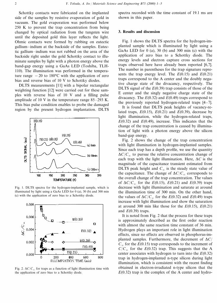
Fig. 1 shows the DLTS spectra for the hydrogen-im-planted sample which is illuminated by light using aGaAs LED for 0 (a), 30 (b) and 300 min (c) with theapplication of zero bias to a Schottky diode. Theenergy levels and electron capture cross sections fortraps observed here have already been reported [6,7].The number in parentheses for the trap signature repre-sents the trap energy level. The E(0.15) and E(0.21)traps correspond to the A center and the doubly nega-tive charge state of the divacancy, respectively. TheDLTS signal of the E(0.39) trap consists of those of theE center and the singly negative charge state of thedivacancy. The E(0.32) and E(0.49) traps correspond tothe previously reported hydrogen-related traps [4–7].
It is found that DLTS peak heights of vacancy-re-lated traps, E(0.15), E(0.21) and E(0.39), decrease bylight illumination, while the hydrogen-related traps,E(0.32) and E(0.49), increase. This indicates that thechange of the trap concentration is caused by illumina-tion of light with a photon energy above the siliconband-gap energy.
Fig. 2 shows the change of the trap concentrationwith light illumination in hydrogen-implanted samples.Since each trap has a depth profile, we use the quantityDC/C� to pursue the relative concentration change ofeach trap with the light illumination. Here, DC is themagnitude of the capacitance transient estimated fromDLTS peak height and C� is the steady state value ofthe capacitance. The change of DC/C� corresponds tothe overall change of the trap concentration. The valuesof DC/C� for the E(0.15), E(0.21) and E(0.39) trapsdecrease with light illumination and saturate at aroundthe illumination time of 300 min. On the other hand,the values of DC/C� for the E(0.32) and E(0.49) trapsincrease with light illumination and show the saturationat around 300 min like those for the E(0.15), E(0.21)and E(0.39) traps.
It is noted from Fig. 2 that the process for these trapsis approximately described as the first order reactionwith almost the same reaction time constant of 36 min.Hydrogen plays an important role in light illuminationeffects, since no effects are observed in phosphorus-im-planted samples. Furthermore, the decrement of DC/C� for the E(0.15) trap corresponds to the increment ofC/C� for the E(0.32) trap. This suggests that the Acenter associates with hydrogen to turn into the E(0.32)trap in hydrogen-implanted n-type silicon during lightillumination, which is consistent with the recent findingobtained in electron-irradiated n-type silicon that theE(0.32) trap is the complex of the A center and hydro-
Fig. 1. DLTS spectra for the hydrogen-implanted sample, which isilluminated by light using a GaAs LED for 0 (a), 30 (b) and 300 min(c) with the application of zero bias to a Schottky diode.
Fig. 2. DC/C� for traps as a function of light illumination time withthe application of zero bias to a Schottky diode.
Y. Tokuda, A. Ito / Materials Science and Engineering B71 (2000) 1–5 3
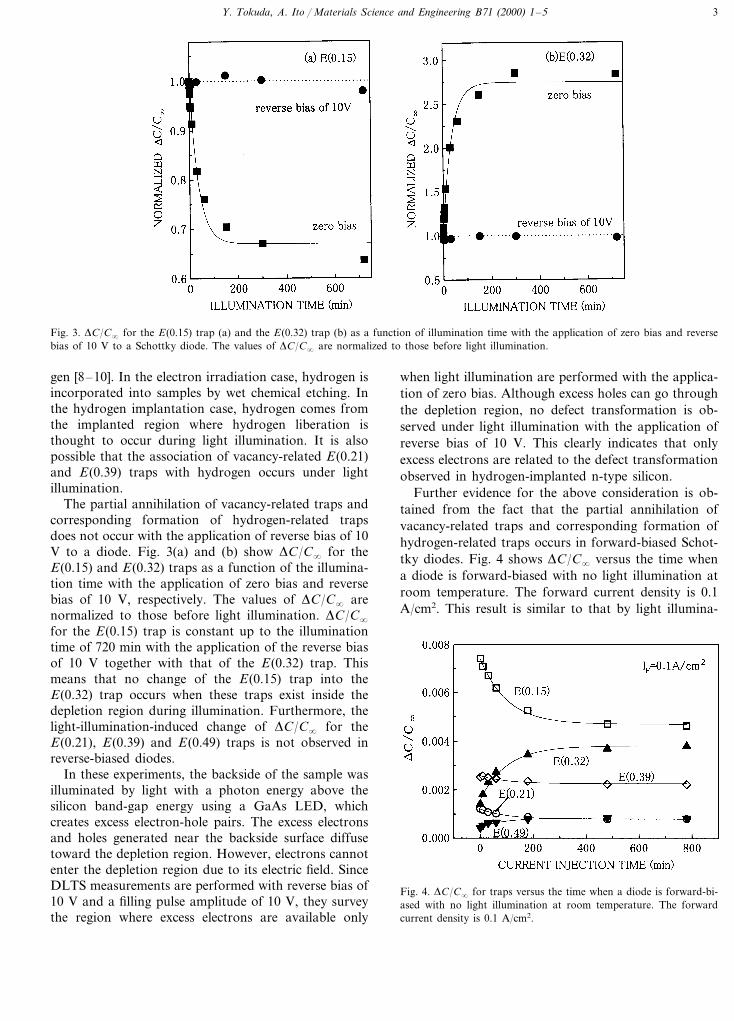
Fig. 3. DC/C� for the E(0.15) trap (a) and the E(0.32) trap (b) as a function of illumination time with the application of zero bias and reversebias of 10 V to a Schottky diode. The values of DC/C� are normalized to those before light illumination.
gen [8–10]. In the electron irradiation case, hydrogen isincorporated into samples by wet chemical etching. Inthe hydrogen implantation case, hydrogen comes fromthe implanted region where hydrogen liberation isthought to occur during light illumination. It is alsopossible that the association of vacancy-related E(0.21)and E(0.39) traps with hydrogen occurs under lightillumination.
The partial annihilation of vacancy-related traps andcorresponding formation of hydrogen-related trapsdoes not occur with the application of reverse bias of 10V to a diode. Fig. 3(a) and (b) show DC/C� for theE(0.15) and E(0.32) traps as a function of the illumina-tion time with the application of zero bias and reversebias of 10 V, respectively. The values of DC/C� arenormalized to those before light illumination. DC/C�for the E(0.15) trap is constant up to the illuminationtime of 720 min with the application of the reverse biasof 10 V together with that of the E(0.32) trap. Thismeans that no change of the E(0.15) trap into theE(0.32) trap occurs when these traps exist inside thedepletion region during illumination. Furthermore, thelight-illumination-induced change of DC/C� for theE(0.21), E(0.39) and E(0.49) traps is not observed inreverse-biased diodes.
In these experiments, the backside of the sample wasilluminated by light with a photon energy above thesilicon band-gap energy using a GaAs LED, whichcreates excess electron-hole pairs. The excess electronsand holes generated near the backside surface diffusetoward the depletion region. However, electrons cannotenter the depletion region due to its electric field. SinceDLTS measurements are performed with reverse bias of10 V and a filling pulse amplitude of 10 V, they surveythe region where excess electrons are available only
when light illumination are performed with the applica-tion of zero bias. Although excess holes can go throughthe depletion region, no defect transformation is ob-served under light illumination with the application ofreverse bias of 10 V. This clearly indicates that onlyexcess electrons are related to the defect transformationobserved in hydrogen-implanted n-type silicon.
Further evidence for the above consideration is ob-tained from the fact that the partial annihilation ofvacancy-related traps and corresponding formation ofhydrogen-related traps occurs in forward-biased Schot-tky diodes. Fig. 4 shows DC/C� versus the time whena diode is forward-biased with no light illumination atroom temperature. The forward current density is 0.1A/cm2. This result is similar to that by light illumina-
Fig. 4. DC/C� for traps versus the time when a diode is forward-bi-ased with no light illumination at room temperature. The forwardcurrent density is 0.1 A/cm2.
Y. Tokuda, A. Ito / Materials Science and Engineering B71 (2000) 1–54
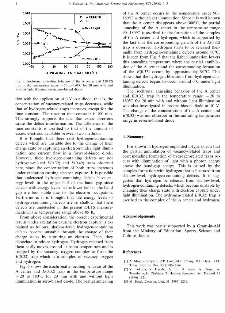
Fig. 5. Isochronal annealing behavior of the A center and E(0.32)trap in the temperature range −20 to 180°C for 20 min with andwithout light illumination in zero-biased diode.
of the A center occurs in the temperature range 90–180°C without light illumination. Since it is well knownthat the A center disappears above 300°C, the partialannealing of the A center in the temperature range90–180°C is ascribed to the formation of the complexof the A center and hydrogen, which is supported bythe fact that the corresponding growth of the E(0.32)trap is observed. Hydrogen starts to be released ther-mally from hydrogen-containing defects around 90°C.It is seen from Fig. 5 that the light illumination lowersthis annealing temperature where the partial annihila-tion of the A center and the corresponding formationof the E(0.32) occurs by approximately 90°C. Thisshows that the hydrogen liberation from hydrogen-con-taining defects begins to occur around 0°C under lightillumination.
The isochronal annealing behavior of the A centerand E(0.32) trap in the temperature range −20 to180°C for 20 min with and without light illuminationwas also investigated in reverse-biased diode at 10 V.The change of the concentration of the A center andE(0.32) was not observed in this annealing temperaturerange in reverse-biased diode.
4. Summary
It is shown in hydrogen-implanted n-type silicon thatthe partial annihilation of vacancy-related traps andcorresponding formation of hydrogen-related traps oc-curs with illumination of light with a photon energyabove the band-gap energy. This is caused by thecomplex formation with hydrogen that is liberated fromshallow-level, hydrogen-containing defects. It is sug-gested that hydrogen be released from shallow-level,hydrogen-containing defects, which become unstable bychanging their charge state with electron capture underlight illumination. The hydrogen-related E(0.32) trap isascribed to the complex of the A center and hydrogen.
Acknowledgements
This work was partly supported by a Grant-in-Aidfrom the Ministry of Education, Sports, Science andCulture, Japan.
References
[1] A. Mogro-Campero, R.P. Love, M.F. Chang, R.F. Dyer, IEEETrans. Electron Dev. 33 (1986) 1667.
[2] Y. Tokuda, Y. Hasabe, A. Ito, H. Iwata, A. Usami, A.Terashima, H. Ohshima, T. Hattori, Semicond. Sci. Technol. 11(1996) 1821.
[3] M. Bruel, Electron. Lett. 31 (1995) 1201.
tion with the application of 0 V to a diode, that is, theconcentration of vacancy-related traps decreases, whilethat of hydrogen-related traps increases, except for thetime constant. The reaction time constant is 100 min.This strongly supports the idea that excess electronscause the defect transformation. The difference of thetime constants is ascribed to that of the amount ofexcess electrons available between two methods.
It is thought that there exist hydrogen-containingdefects which are unstable due to the change of theircharge state by capturing an electron under light illumi-nation and current flow in a forward-biased diode.However, these hydrogen-containing defects are nothydrogen-related E(0.32) and E(0.49) traps observedhere, since the concentration of both traps increasesunder excitation causing electron capture. It is possiblethat undetected hydrogen-containing defects have en-ergy levels in the upper half of the band gap sincedefects with energy levels in the lower half of the bandgap are less stable due to the electron occupation.Furthermore, it is thought that the energy levels ofhydrogen-containing defects are so shallow that thesedefects are undetected in the present DLTS measure-ments in the temperature range above 85 K.
From above consideration, the present experimentalresults under excitation causing electron capture is ex-plained as follows; shallow-level, hydrogen-containingdefects become unstable through the change of theircharge states by capturing an electron. Then, theydissociate to release hydrogen. Hydrogen released fromthem easily moves around at room temperature and istrapped by the vacancy–oxygen complex to form theE(0.32) trap which is a complex of vacancy–oxygenand hydrogen.
Fig. 5 shows the isochronal annealing behavior of theA center and E(0.32) trap in the temperature range−20 to 180°C for 20 min with and without lightillumination in zero-biased diode. The partial annealing
Y. Tokuda, A. Ito / Materials Science and Engineering B71 (2000) 1–5 5
[4] B.G. Svensson, A. Hallen, B.U.R. Sundqvist, Mater. Sci. Eng.B4 (1989) 285.
[5] L. Palmetshofer, J. Reisinger, J. Appl. Phys. 72 (1992) 2167.[6] A. Ito, Y. Tokuda, J. Appl. Phys. 82 (1997) 1053.[7] Y. Tokuda, A. Ito, H. Ohshima, Inst. Phys. Conf. Ser. 160
(1997) 305.[8] O.V. Feklisova, N. Yarykin, Semicond. Sci. Techmpl. 12 (1997)
742.
[9] Y. Tokuda, Jpn. J. Appl. Phys. 37 (1998) 1815.[10] Y. Tokuda, H. Shimada, in: N.H. Nickel, W.B. Jackson, R.C.
Bowman, R.G. Leisure (Eds.), Hydrogen in Semiconductors andMetals, Materials Research Society Symposium Proceedings, vol.513, Materials Research Society, Warrendale, PA, 1998, p. 363.
[11] D.V. Lang, J. Appl. Phys. 45 (1974) 3023.[12] Y. Tokuda, N. Shimizu, A. Usami, Jpn. J. Appl. Phys. 18 (1979)
309.
.