Embed Size (px)
Citation preview
1
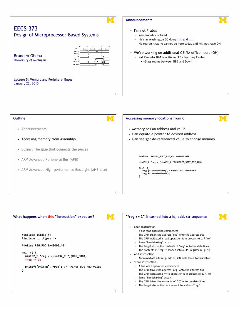
EECS 373Design of Microprocessor-Based Systems
Branden GhenaUniversity of Michigan
Lecture 5: Memory and Peripheral BusesJanuary 22, 2015
2
Announcements
• I’m not Prabal– You probably noticed– He’s in Washington DC doing this and this– He regrets that he cannot be here today and will not have OH
• We’re working on additional GSI/IA office hours (OH)– Pat Pannuto 10-11am MW in EECS Learning Center
• (Glass rooms between BBB and Dow)
3
Outline
• Announcements
• Accessing memory from Assembly/C
• Busses: The glue that connects the pieces
• ARM Advanced Peripheral Bus (APB)
• ARM Advanced High-performance Bus Light (AHB-Lite)
4
#define SYSREG_SOFT_RST_CR 0xE0042030
uint32_t *reg = (uint32_t *)(SYSREG_SOFT_RST_CR);
main () {*reg |= 0x00004000; // Reset GPIO hardware*reg &= ~(0x00004000);
}
Accessing memory locations from C
• Memory has an address and value• Can equate a pointer to desired address • Can set/get de-referenced value to change memory
5
#include <stdio.h>#include <inttypes.h>
#define REG_FOO 0x40000140
main () {uint32_t *reg = (uint32_t *)(REG_FOO);*reg += 3;
printf(“0x%x\n”, *reg); // Prints out new value}
What happens when this “instruction” executes?
6
“*reg += 3” is turned into a ld, add, str sequence
• Load instruction– A bus read operation commences– The CPU drives the address “reg” onto the address bus– The CPU indicated a read operation is in process (e.g. R/W#)– Some “handshaking” occurs– The target drives the contents of “reg” onto the data lines– The contents of “reg” is loaded into a CPU register (e.g. r0)
• Add instruction– An immediate add (e.g. add r0, #3) adds three to this value
• Store instruction– A bus write operation commences– The CPU drives the address “reg” onto the address bus– The CPU indicated a write operation is in process (e.g. R/W#)– Some “handshaking” occurs– The CPU drives the contents of “r0” onto the data lines– The target stores the data value into address “reg”
7
Some useful C keywords
• const– Makes variable value or pointer parameter unmodifiable– const foo = 32;
• register– Tells compiler to locate variables in a CPU register if possible– register int x;
• static– Preserve variable value after its scope ends– Does not go on the stack– static int x;
• volatile– Opposite of const– Can be changed in the background– volatile int I;
8
Outline
• Announcements
• Accessing memory from Assembly/C
• Busses: The glue that connects the pieces
• ARM Advanced Peripheral Bus (APB)
• ARM Advanced High-performance Bus Light (AHB-Lite)
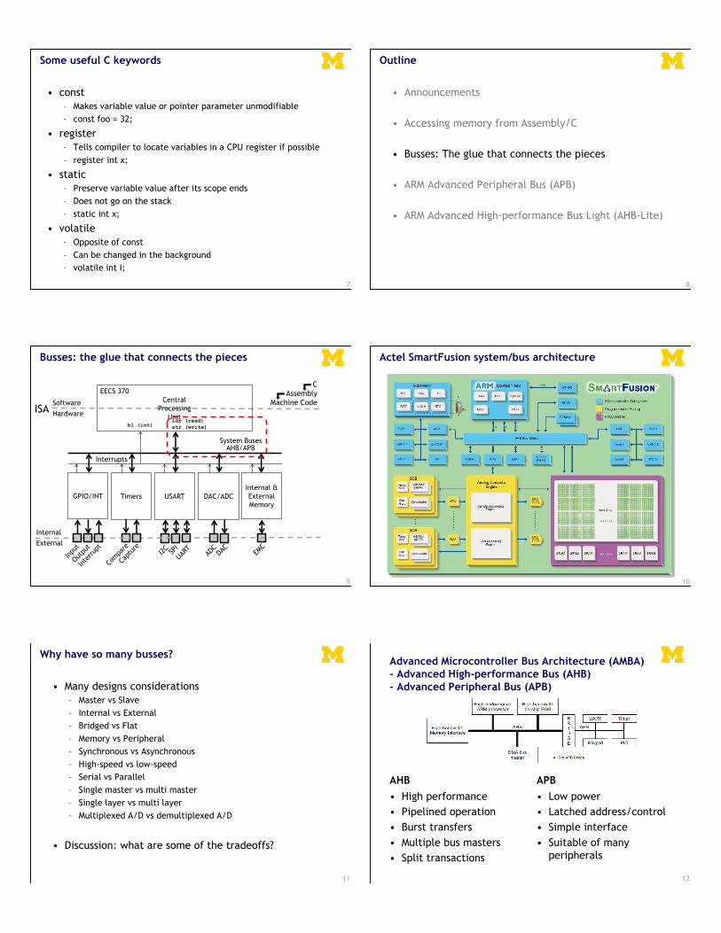
Busses: the glue that connects the pieces
9
Timers
CentralProcessing
Unit
SoftwareHardware
InternalExternal
System BusesAHB/APB
ldr (read)str (write)
ISA
EECS 370
USART DAC/ADCInternal &ExternalMemory
GPIO/INT
CAssembly
Machine Code
Interrupts
bl (int)
10
Actel SmartFusion system/bus architecture
11
Why have so many busses?
• Many designs considerations– Master vs Slave– Internal vs External– Bridged vs Flat– Memory vs Peripheral– Synchronous vs Asynchronous– High-speed vs low-speed– Serial vs Parallel– Single master vs multi master– Single layer vs multi layer– Multiplexed A/D vs demultiplexed A/D
• Discussion: what are some of the tradeoffs?
Advanced Microcontroller Bus Architecture (AMBA)- Advanced High-performance Bus (AHB)- Advanced Peripheral Bus (APB)
AHB• High performance• Pipelined operation• Burst transfers• Multiple bus masters• Split transactions
APB• Low power• Latched address/control• Simple interface• Suitable of many
peripherals
12
13
Outline
• Announcements
• Accessing memory from Assembly/C
• Busses: The glue that connects the pieces
• ARM Advanced Peripheral Bus (APB)
• ARM Advanced High-performance Bus Light (AHB-Lite)
14
APB: a simple bus that is easy to work with
• Low-cost
• Low-power
• Low-complexity
• Low-bandwidth
• Non-pipelined
• Ideal for peripherals
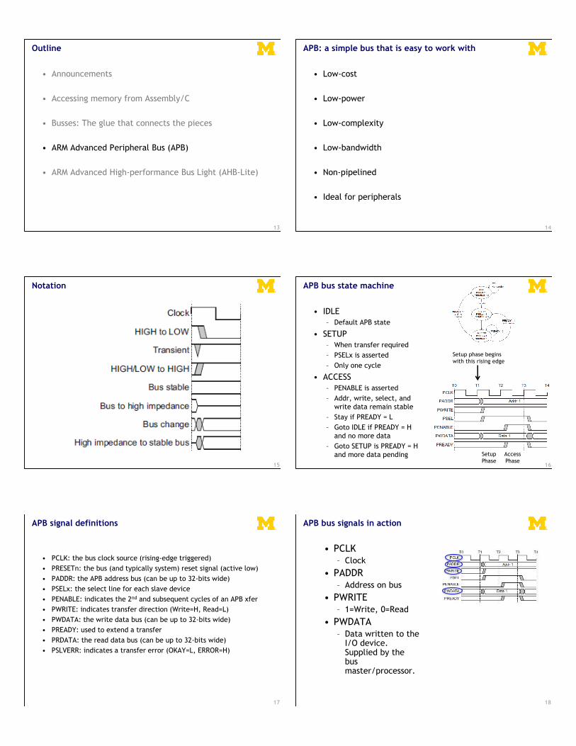
Notation
15 16
APB bus state machine
• IDLE– Default APB state
• SETUP– When transfer required– PSELx is asserted– Only one cycle
• ACCESS– PENABLE is asserted– Addr, write, select, and
write data remain stable– Stay if PREADY = L– Goto IDLE if PREADY = H
and no more data– Goto SETUP is PREADY = H
and more data pending
Setup phase beginswith this rising edge
SetupPhase
AccessPhase
17
APB signal definitions
• PCLK: the bus clock source (rising-edge triggered)• PRESETn: the bus (and typically system) reset signal (active low)• PADDR: the APB address bus (can be up to 32-bits wide)• PSELx: the select line for each slave device• PENABLE: indicates the 2nd and subsequent cycles of an APB xfer• PWRITE: indicates transfer direction (Write=H, Read=L)• PWDATA: the write data bus (can be up to 32-bits wide)• PREADY: used to extend a transfer• PRDATA: the read data bus (can be up to 32-bits wide)• PSLVERR: indicates a transfer error (OKAY=L, ERROR=H)
APB bus signals in action
• PCLK – Clock
• PADDR– Address on bus
• PWRITE– 1=Write, 0=Read
• PWDATA– Data written to the
I/O device. Supplied by the bus master/processor.
18
APB bus signals
• PSEL– Asserted if the current
bus transaction is targeted to this device
• PENABLE– High during entire
transaction other thanthe first cycle.
• PREADY– Driven by target.
Similar to our #ACK. Indicates if the target is ready to do transaction.Each target has it’s own PREADY
19 20
A write transfer with no wait states
Setup phase beginswith this rising edge
SetupPhase
AccessPhase
21
A write transfer with wait states
Setup phase beginswith this rising edge
SetupPhase
AccessPhase
WaitState
WaitState
22
A read transfer with no wait states
Setup phase beginswith this rising edge
SetupPhase
AccessPhase
23
A read transfer with wait states
Setup phase beginswith this rising edge
SetupPhase
AccessPhase
WaitState
WaitState
Example setup
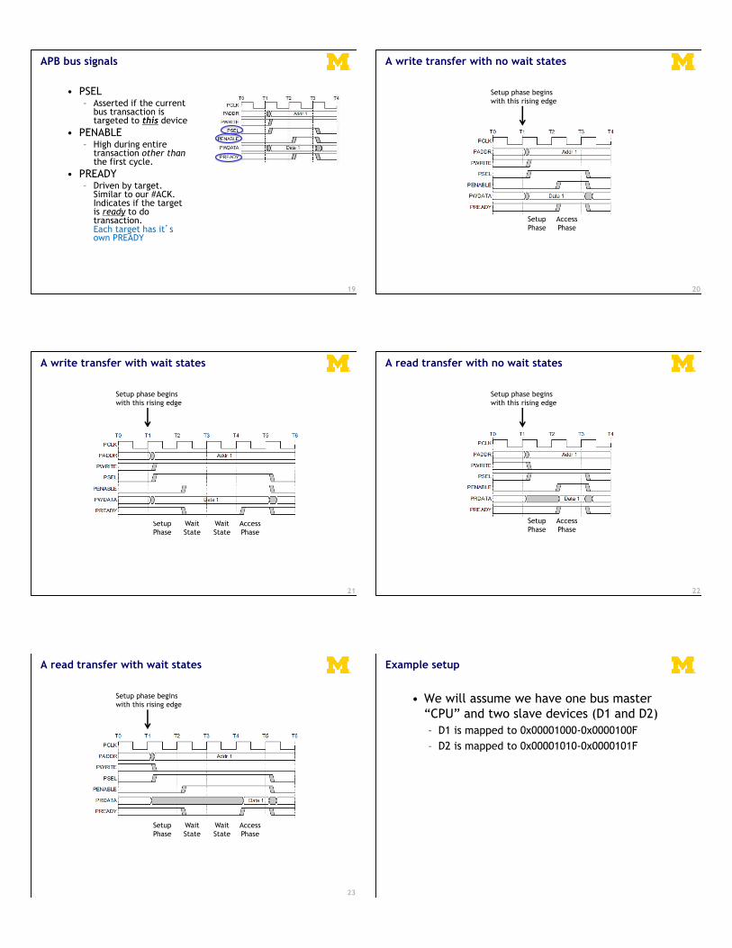
• We will assume we have one bus master “CPU” and two slave devices (D1 and D2)– D1 is mapped to 0x00001000-0x0000100F – D2 is mapped to 0x00001010-0x0000101F
CPU stores to location 0x00001004 with no stalls
25
D1
D2
Writes
Let’s do some hardware examples!
26
Design a device which writes to a register wheneverany address in its range is written
27
32-bit Reg
D[31:0] Q[31:0]
EN
C
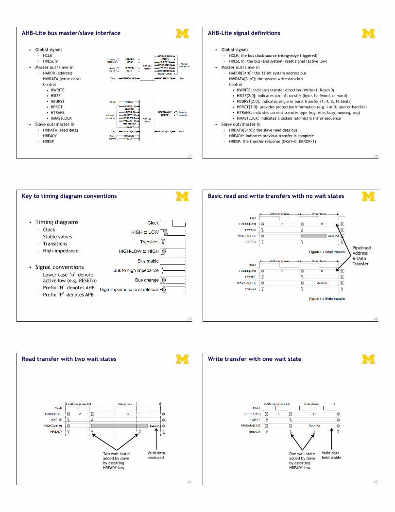
We are assuming APB only gets lowest 8 bits of address here…
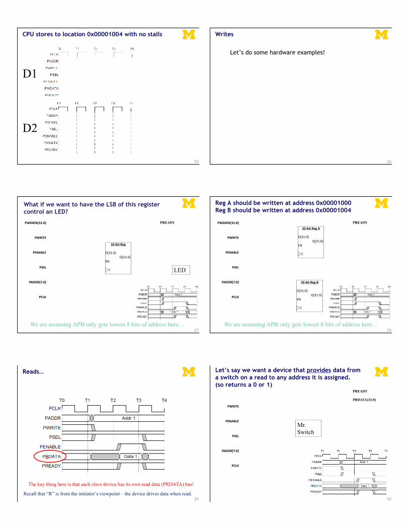
What if we want to have the LSB of this register control an LED?
PREADYPWDATA[31:0]
PWRITE
PENABLE
PSEL
PADDR[7:0]
PCLK
LED
Reg A should be written at address 0x00001000Reg B should be written at address 0x00001004
28
32-bit Reg A
D[31:0] Q[31:0]
EN
C
We are assuming APB only gets lowest 8 bits of address here…
32-bit Reg B
D[31:0] Q[31:0]
EN
C
PREADYPWDATA[31:0]
PWRITE
PENABLE
PSEL
PADDR[7:0]
PCLK
Reads…
29
The key thing here is that each slave device has its own read data (PRDATA) bus!
Recall that “R” is from the initiator’s viewpoint—the device drives data when read.
Let’s say we want a device that provides data froma switch on a read to any address it is assigned. (so returns a 0 or 1)
30
Mr. Switch
PWRITE
PENABLE
PSEL
PADDR[7:0]
PCLK
PREADY
PRDATA[32:0]
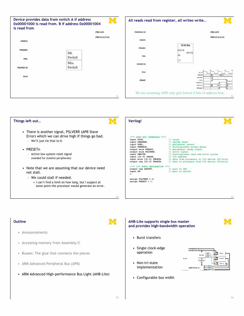
Device provides data from switch A if address 0x00001000 is read from. B if address 0x00001004is read from
31
Mr.SwitchMrs.Switch
PWRITE
PENABLE
PSEL
PADDR[7:0]
PCLK
PREADY
PRDATA[31:0]
All reads read from register, all writes write…
32
PWDATA[31:0]
PWRITE
PENABLE
PSEL
PADDR[7:0]
PCLK
PREADY
32-bit Reg
D[31:0] Q[31:0]
EN
C
We are assuming APB only gets lowest 8 bits of address here…
PREADY
PRDATA[31:0]
Things left out…
• There is another signal, PSLVERR (APB Slave Error) which we can drive high if things go bad.– We’ll just tie that to 0.
• PRESETn– Active low system reset signal– (needed for stateful peripherals)
• Note that we are assuming that our device need not stall.– We could stall if needed.
• I can’t find a limit on how long, but I suspect at some point the processor would generate an error.
33
Verilog!
34
/*** APB3 BUS INTERFACE ***/ input PCLK, // clock input PRESERN, // system reset input PSEL, // peripheral select input PENABLE, // distinguishes access phase output wire PREADY, // peripheral ready signal output wire PSLVERR, // error signal input PWRITE, // distinguishes read and write cycles input [31:0] PADDR, // I/O address input wire [31:0] PWDATA, // data from processor to I/O device (32 bits) output reg [31:0] PRDATA, // data to processor from I/O device (32-bits) /*** I/O PORTS DECLARATION ***/ output reg LEDOUT, // port to LED input SW // port to switch ); assign PSLVERR = 0; assign PREADY = 1;
35
Outline
• Announcements
• Accessing memory from Assembly/C
• Busses: The glue that connects the pieces
• ARM Advanced Peripheral Bus (APB)
• ARM Advanced High-performance Bus Light (AHB-Lite)
36
AHB-Lite supports single bus masterand provides high-bandwidth operation
• Burst transfers
• Single clock-edge operation
• Non-tri-state implementation
• Configurable bus width
37
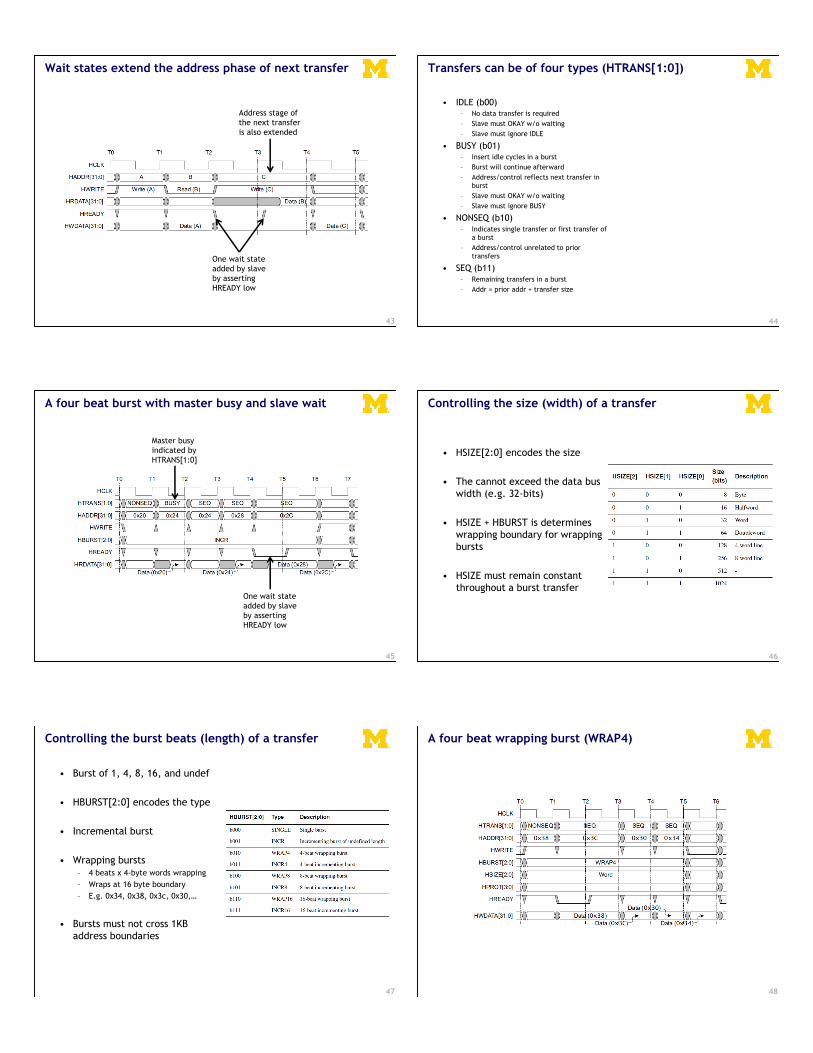
AHB-Lite bus master/slave interface
• Global signals– HCLK– HRESETn
• Master out/slave in– HADDR (address)– HWDATA (write data)– Control
• HWRITE• HSIZE• HBURST• HPROT• HTRANS• HMASTLOCK
• Slave out/master in– HRDATA (read data)– HREADY– HRESP
38
AHB-Lite signal definitions
• Global signals– HCLK: the bus clock source (rising-edge triggered)– HRESETn: the bus (and system) reset signal (active low)
• Master out/slave in– HADDR[31:0]: the 32-bit system address bus– HWDATA[31:0]: the system write data bus– Control
• HWRITE: indicates transfer direction (Write=1, Read=0)• HSIZE[2:0]: indicates size of transfer (byte, halfword, or word)• HBURST[2:0]: indicates single or burst transfer (1, 4, 8, 16 beats)• HPROT[3:0]: provides protection information (e.g. I or D; user or handler)• HTRANS: indicates current transfer type (e.g. idle, busy, nonseq, seq)• HMASTLOCK: indicates a locked (atomic) transfer sequence
• Slave out/master in– HRDATA[31:0]: the slave read data bus– HREADY: indicates previous transfer is complete– HRESP: the transfer response (OKAY=0, ERROR=1)
39
Key to timing diagram conventions
• Timing diagrams– Clock– Stable values– Transitions– High-impedance
• Signal conventions– Lower case ‘n’ denote
active low (e.g. RESETn)– Prefix ‘H’ denotes AHB– Prefix ‘P’ denotes APB
40
Basic read and write transfers with no wait states
PipelinedAddress& DataTransfer
41
Read transfer with two wait states
Two wait statesadded by slaveby assertingHREADY low
Valid dataproduced
42
Write transfer with one wait state
One wait stateadded by slaveby assertingHREADY low
Valid dataheld stable
43
Wait states extend the address phase of next transfer
One wait stateadded by slaveby assertingHREADY low
Address stage of the next transferis also extended
44
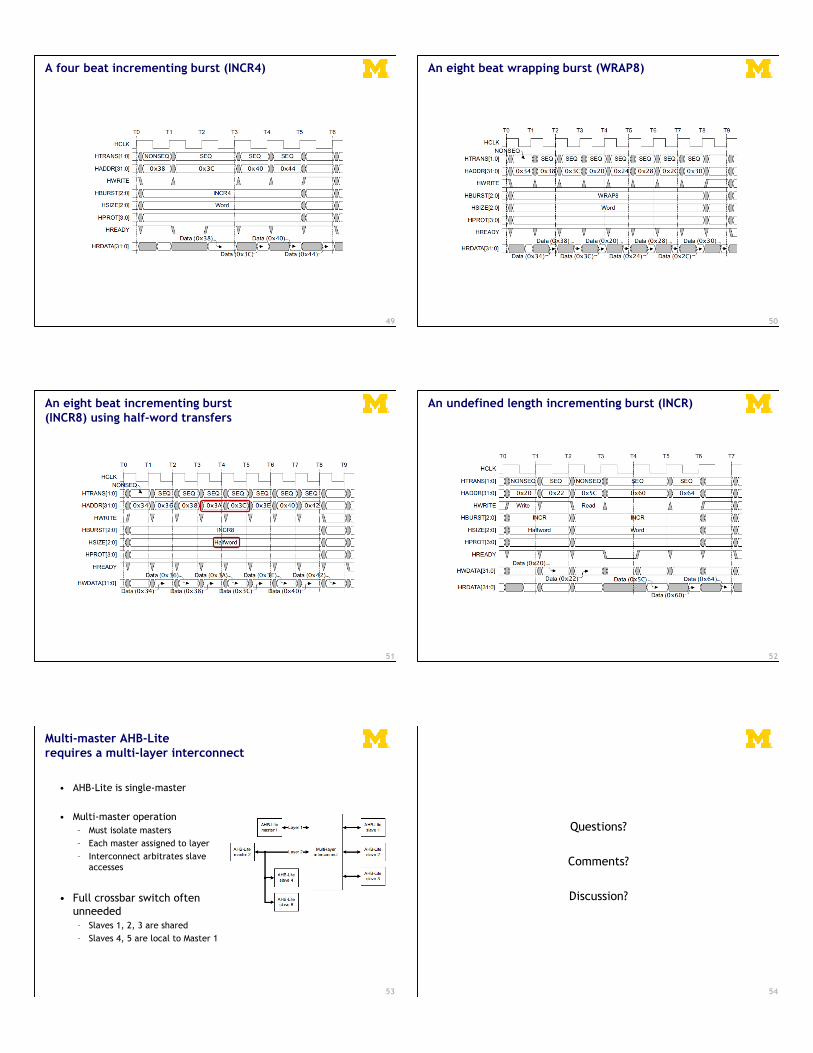
Transfers can be of four types (HTRANS[1:0])
• IDLE (b00)– No data transfer is required– Slave must OKAY w/o waiting– Slave must ignore IDLE
• BUSY (b01)– Insert idle cycles in a burst– Burst will continue afterward– Address/control reflects next transfer in
burst– Slave must OKAY w/o waiting– Slave must ignore BUSY
• NONSEQ (b10)– Indicates single transfer or first transfer of
a burst– Address/control unrelated to prior
transfers
• SEQ (b11)– Remaining transfers in a burst– Addr = prior addr + transfer size
45
A four beat burst with master busy and slave wait
One wait stateadded by slaveby assertingHREADY low
Master busyindicated byHTRANS[1:0]
46
Controlling the size (width) of a transfer
• HSIZE[2:0] encodes the size
• The cannot exceed the data bus width (e.g. 32-bits)
• HSIZE + HBURST is determines wrapping boundary for wrapping bursts
• HSIZE must remain constant throughout a burst transfer
47
Controlling the burst beats (length) of a transfer
• Burst of 1, 4, 8, 16, and undef
• HBURST[2:0] encodes the type
• Incremental burst
• Wrapping bursts – 4 beats x 4-byte words wrapping– Wraps at 16 byte boundary– E.g. 0x34, 0x38, 0x3c, 0x30,…
• Bursts must not cross 1KB address boundaries
48
A four beat wrapping burst (WRAP4)
49
A four beat incrementing burst (INCR4)
50
An eight beat wrapping burst (WRAP8)
51
An eight beat incrementing burst(INCR8) using half-word transfers
52
An undefined length incrementing burst (INCR)
53
Multi-master AHB-Lite requires a multi-layer interconnect
• AHB-Lite is single-master
• Multi-master operation– Must isolate masters– Each master assigned to layer– Interconnect arbitrates slave
accesses
• Full crossbar switch often unneeded– Slaves 1, 2, 3 are shared– Slaves 4, 5 are local to Master 1
54
Questions?
Comments?
Discussion?