Embed Size (px)
Citation preview
C A R B O N 4 6 ( 2 0 0 8 ) 1 4 3 5 – 1 4 4 2
. sc iencedi rec t . com
ava i lab le a t wwwjournal homepage: www.elsevier .com/ locate /carbon
Anomalies in thickness measurements of grapheneand few layer graphite crystals by tapping modeatomic force microscopy
P. Nemes-Incze*,a, Z. Osvatha, K. Kamarasb, L.P. Biroa
aResearch Institute for Technical Physics and Materials Science, Hungarian Academy of Sciences, H-1525 Budapest, P.O. Box 49, HungarybResearch Institute for Solid State Physics and Optics, Hungarian Academy of Sciences, H-1525 Budapest, P.O. Box 49, Hungary
A R T I C L E I N F O
Article history:
Received 28 April 2008
Accepted 7 June 2008
Available online 17 June 2008
0008-6223/$ - see front matter � 2008 Elsevidoi:10.1016/j.carbon.2008.06.022
* Corresponding author: Fax: +36 1 3922226.E-mail address: [email protected] (P. N
A B S T R A C T
Atomic Force Microscopy (AFM) in the tapping (intermittent contact) mode is a commonly
used tool to measure the thickness of graphene and few layer graphene (FLG) flakes on sil-
icon oxide surfaces. It is a convenient tool to quickly determine the thickness of individual
FLG films. However, reports from literature show a large variation of the measured thick-
ness of graphene layers. This paper is focused on the imaging mechanism of tapping mode
AFM (TAFM) when measuring graphene and FLG thickness, and we show that at certain
measurement parameters significant deviations can be introduced in the measured thick-
ness of FLG flakes. An increase of as much as 1 nm can be observed in the measured height
of FLG crystallites, when using an improperly chosen range of free amplitude values of the
tapping cantilever. We present comparative Raman spectroscopy and TAFM measurements
on selected single and multilayer graphene films, based on which we suggest ways to cor-
rectly measure graphene and FLG thickness using TAFM.
� 2008 Elsevier Ltd. All rights reserved.
1. Introduction
Graphene, as a building block of graphite has been theoreti-
cally investigated since the 1940s [1]. Until 2004, when Nov-
oselov et al. successfully identified graphene [2] and other
2D crystals [3] in a simple tabletop experiment, it was as-
sumed that 2D crystals were thermodynamically unstable
and could not exist under ambient conditions [4,5]. The dis-
covery that such samples can be produced has led to a wealth
of scientific investigation [6–11], due to the very promising
electronic [12] and mechanical properties of graphene, fur-
thermore due to it’s resistance to mechanical and chemical
stress and it’s high crystallinity [3].
Today, the most successful method to prepare graphene
samples is mechanical exfoliation of graphite onto oxidized
Si wafers [2]. The thickness of few layer graphite (FLG) films
is estimated by optical microscopy [13,14], after which the
er Ltd. All rights reservedemes-Incze).
thickness of the thinnest crystallites is measured by AFM.
Much like other scanning probe techniques, AFM is not free
of measurement artefacts. With AFM being such a widely em-
ployed tool to inspect the thickness of FLG crystals, we believe
that a detailed investigation of the possible sources of errors
in the AFM measurement of FLG thickness is of great impor-
tance. When measuring features of the order of magnitude
of one atomic layer and changing material properties, effects
of lesser importance under other circumstances (like homo-
geneous samples), may play a crucial role in distorting topog-
raphy images. Indeed various groups reported different
thickness measurements for graphene layers, with thickness-
es ranging from 0.35 to 1 nm, relative to the SiO2 substrate.
Novoselov et al. measured platelet thicknesses of 1–1.6 nm
[2]. Gupta et al. have measured an instrumental offset in-
duced by the AFM, of 0.33 nm, i.e., 0.7 nm height for a single
layer [20]. Other authors have also reported varying step
.
1436 C A R B O N 4 6 ( 2 0 0 8 ) 1 4 3 5 – 1 4 4 2
heights for FLG supported on silicon oxide [15,16,23]. This var-
iation in the thickness of the single graphene layers may be
attributed to the change in the tip–sample interaction as the
tapping tip scans over the surface. Observations of distortions
in the thickness of nanoparticles, measured with TAFM, are
well known. Anomalous nanoparticle height measurements,
dependent on the free amplitude of the cantilever and mate-
rial properties of the sample, were reported earlier [17–19].
It is generally accepted that folded regions in the graphene
give the most reliable measurement of thickness [3], however
such folded regions are not always available in every experi-
ment. Furthermore, samples of good quality should not con-
tain such regions, leaving no option, but to check the
thickness relative to the oxide surface. Recently, Raman scat-
tering [20–22] and Rayleigh scattering [23] have been shown to
be useful tools in determining the number of graphene layers
in a given sample, and other optical techniques are showing
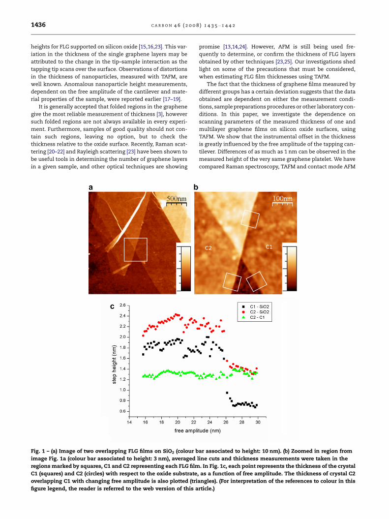
Fig. 1 – (a) Image of two overlapping FLG films on SiO2 (colour b
image Fig. 1a (colour bar associated to height: 3 nm), averaged
regions marked by squares, C1 and C2 representing each FLG film
C1 (squares) and C2 (circles) with respect to the oxide substrate
overlapping C1 with changing free amplitude is also plotted (tri
figure legend, the reader is referred to the web version of this a
promise [13,14,24]. However, AFM is still being used fre-
quently to determine, or confirm the thickness of FLG layers
obtained by other techniques [23,25]. Our investigations shed
light on some of the precautions that must be considered,
when estimating FLG film thicknesses using TAFM.
The fact that the thickness of graphene films measured by
different groups has a certain deviation suggests that the data
obtained are dependent on either the measurement condi-
tions, sample preparations procedures or other laboratory con-
ditions. In this paper, we investigate the dependence on
scanning parameters of the measured thickness of one and
multilayer graphene films on silicon oxide surfaces, using
TAFM. We show that the instrumental offset in the thickness
is greatly influenced by the free amplitude of the tapping can-
tilever. Differences of as much as 1 nm can be observed in the
measured height of the very same graphene platelet. We have
compared Raman spectroscopy, TAFM and contact mode AFM
ar associated to height: 10 nm). (b) Zoomed in region from
line cuts and thickness measurements were taken in the
. In Fig. 1c, each point represents the thickness of the crystal
, as a function of free amplitude. The thickness of crystal C2
angles). (For interpretation of the references to colour in this
rticle.)
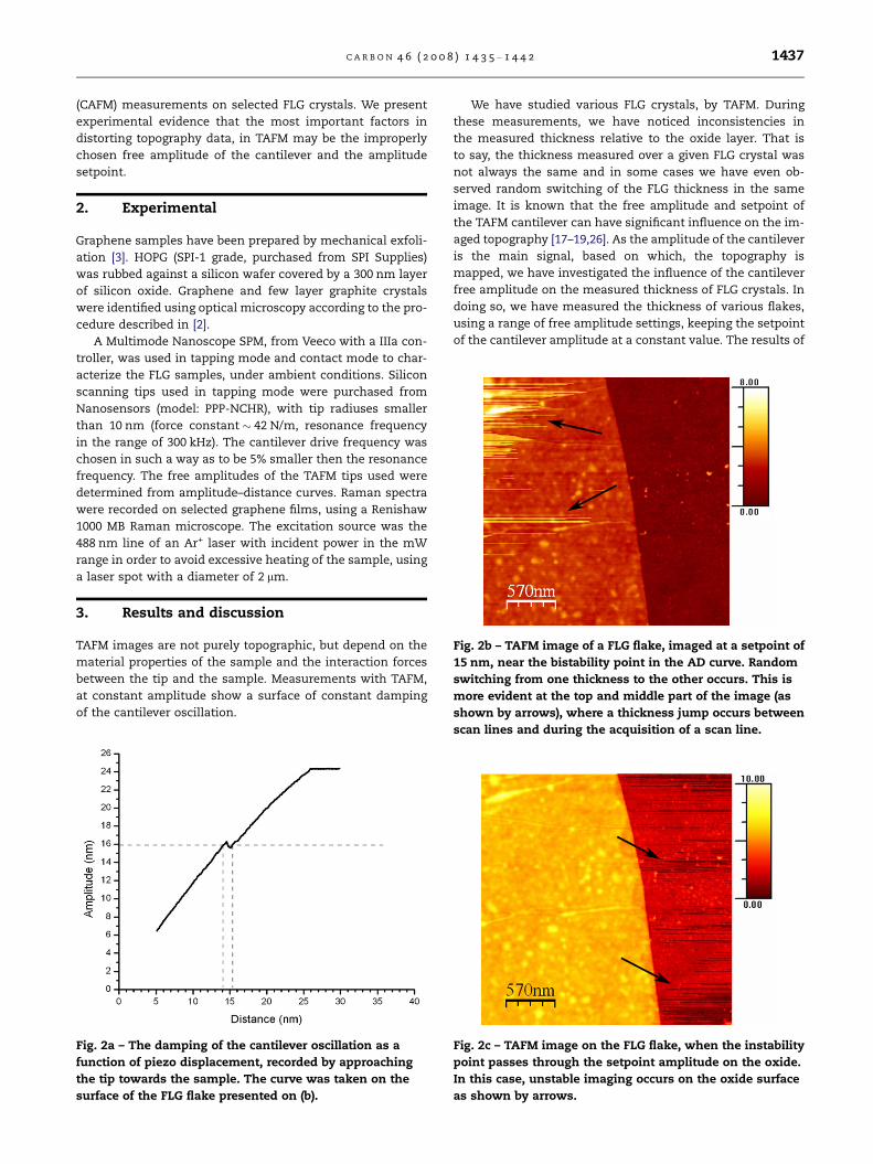
Fig. 2b – TAFM image of a FLG flake, imaged at a setpoint of
15 nm, near the bistability point in the AD curve. Random
switching from one thickness to the other occurs. This is
more evident at the top and middle part of the image (as
shown by arrows), where a thickness jump occurs between
C A R B O N 4 6 ( 2 0 0 8 ) 1 4 3 5 – 1 4 4 2 1437
(CAFM) measurements on selected FLG crystals. We present
experimental evidence that the most important factors in
distorting topography data, in TAFM may be the improperly
chosen free amplitude of the cantilever and the amplitude
setpoint.
2. Experimental
Graphene samples have been prepared by mechanical exfoli-
ation [3]. HOPG (SPI-1 grade, purchased from SPI Supplies)
was rubbed against a silicon wafer covered by a 300 nm layer
of silicon oxide. Graphene and few layer graphite crystals
were identified using optical microscopy according to the pro-
cedure described in [2].
A Multimode Nanoscope SPM, from Veeco with a IIIa con-
troller, was used in tapping mode and contact mode to char-
acterize the FLG samples, under ambient conditions. Silicon
scanning tips used in tapping mode were purchased from
Nanosensors (model: PPP-NCHR), with tip radiuses smaller
than 10 nm (force constant � 42 N/m, resonance frequency
in the range of 300 kHz). The cantilever drive frequency was
chosen in such a way as to be 5% smaller then the resonance
frequency. The free amplitudes of the TAFM tips used were
determined from amplitude–distance curves. Raman spectra
were recorded on selected graphene films, using a Renishaw
1000 MB Raman microscope. The excitation source was the
488 nm line of an Ar+ laser with incident power in the mW
range in order to avoid excessive heating of the sample, using
a laser spot with a diameter of 2 lm.
3. Results and discussion
TAFM images are not purely topographic, but depend on the
material properties of the sample and the interaction forces
between the tip and the sample. Measurements with TAFM,
at constant amplitude show a surface of constant damping
of the cantilever oscillation.
Fig. 2a – The damping of the cantilever oscillation as a
function of piezo displacement, recorded by approaching
the tip towards the sample. The curve was taken on the
surface of the FLG flake presented on (b).
We have studied various FLG crystals, by TAFM. During
these measurements, we have noticed inconsistencies in
the measured thickness relative to the oxide layer. That is
to say, the thickness measured over a given FLG crystal was
not always the same and in some cases we have even ob-
served random switching of the FLG thickness in the same
image. It is known that the free amplitude and setpoint of
the TAFM cantilever can have significant influence on the im-
aged topography [17–19,26]. As the amplitude of the cantilever
is the main signal, based on which, the topography is
mapped, we have investigated the influence of the cantilever
free amplitude on the measured thickness of FLG crystals. In
doing so, we have measured the thickness of various flakes,
using a range of free amplitude settings, keeping the setpoint
of the cantilever amplitude at a constant value. The results of
scan lines and during the acquisition of a scan line.
Fig. 2c – TAFM image on the FLG flake, when the instability
point passes through the setpoint amplitude on the oxide.
In this case, unstable imaging occurs on the oxide surface
as shown by arrows.

1438 C A R B O N 4 6 ( 2 0 0 8 ) 1 4 3 5 – 1 4 4 2
such a measurement can be seen in Fig. 1. Two FLG crystals
were measured simultaneously, one overlapping the other.
The free amplitude was varied from 16 to 30 nm. For each free
amplitude setting a complete AFM image was acquired and
the step heights in three regions were evaluated (marked by
white squares): crystal C1–oxide; crystal C2–oxide and C2
overlapping C1. Starting with the 16 nm free amplitude and
keeping the setpoint constant, we have observed that at
26 nm free amplitude, the thickness measured on top of the
oxide surface decreases almost instantly, by about 0.8–1 nm.
However, the thickness measured at the overlapping region
of FLG C2 (green triangles) stays constant. This shows, in
accordance with reports from literature that a more reliable
measure of thickness is the step height relative to another
graphite substrate. The effect described here was checked
on various FLG crystals, using different scanning tips. In each
case, the effect could be observed, to a greater or minor de-
gree, with deviations in the thickness measured at low free
amplitudes.
The presence of two ‘‘stable’’ thickness values hints at the
existence of a biostability in the measurement system. To
further investigate the phenomenon, we have measured
amplitude–distance (AD) curves on a FLG surface and the
neighbouring oxide substrate, using a range of free ampli-
tudes. The curves were obtained by reducing the tip–sample
distance from a value larger than the free amplitude to a min-
imal separation, where the amplitude was reduced to about
10% of the free amplitude. The amplitude was not reduced to
zero because in this manner the reproducibility of the AD
curves was poor [27].
A typical AD curve is plotted on Fig. 2a, recorded on an FLG
surface, at 25.8 nm free amplitude. The striking feature of the
amplitude curve is that at the amplitude value of 16 nm a
Fig. 3 – AD curves on the FLG (a) and oxide (b) surface at differe
amplitude shows the setpoint used during measurements. At 2
amplitude. For the oxide surface such a crossing is experienced
jump can be observed. In this region, two different piezo dis-
placement values correspond to the same amplitude, the dif-
ference being about 1 nm. This is important because the
feedback electronics of the AFM works correctly only for a lin-
ear signal. If the measurement setpoint is selected in such a
way as to coincide with the jump in amplitude, the feedback
electronics may produce random switching from one dis-
placement value to the other [26]. Since the height signal is
derived from the piezo displacement signal, random switch-
ing in height occurs. This behaviour is presented in Figs. 2b
and 2c on a FLG film. In one case Fig. 2b, the imaging is stable
on silicon oxide, while in Fig. 2c, stable imaging is achieved
over the FLG.
Changes in topography of such a magnitude (�1 nm) have
been reported previously by Kuhle et al. [19] on Cu clusters
supported on a silicon oxide substrate. The origin of this
change in topography, as reported by the authors, is a jump
in the amplitude response of the cantilever, with changing
tip–sample separation, as seen on Fig. 2a. Anczykowski et
al., using time resolved numerical simulation of the tapping
tip [28] pointed out that the jump in amplitude marks a change
in the sign of the tip–sample interaction force. When the tip
starts to approach the sample, the amplitude decreases line-
arly. In this regime, long range attractive forces are responsible
for the oscillation damping. At a certain tip–sample separation
a jump occurs in the amplitude (see Fig. 2a). This jump marks
the onset of a region where, with further decreasing tip–sam-
ple distance, both long range attractive and short range repul-
sive forces act on the tip, i.e. the tip is in hard mechanical
contact with the sample. After the jump, the damping of the
oscillation increases further, but this time net repulsive forces
characterize the tip–sample interaction and the contact time
of the tip also produces a jump [29].
nt free amplitudes (24, 26, 28.5 nm). Dashed line at 15 nm
6 nm free amplitude the setpoint crosses the jump in
at free amplitudes around 21 nm.
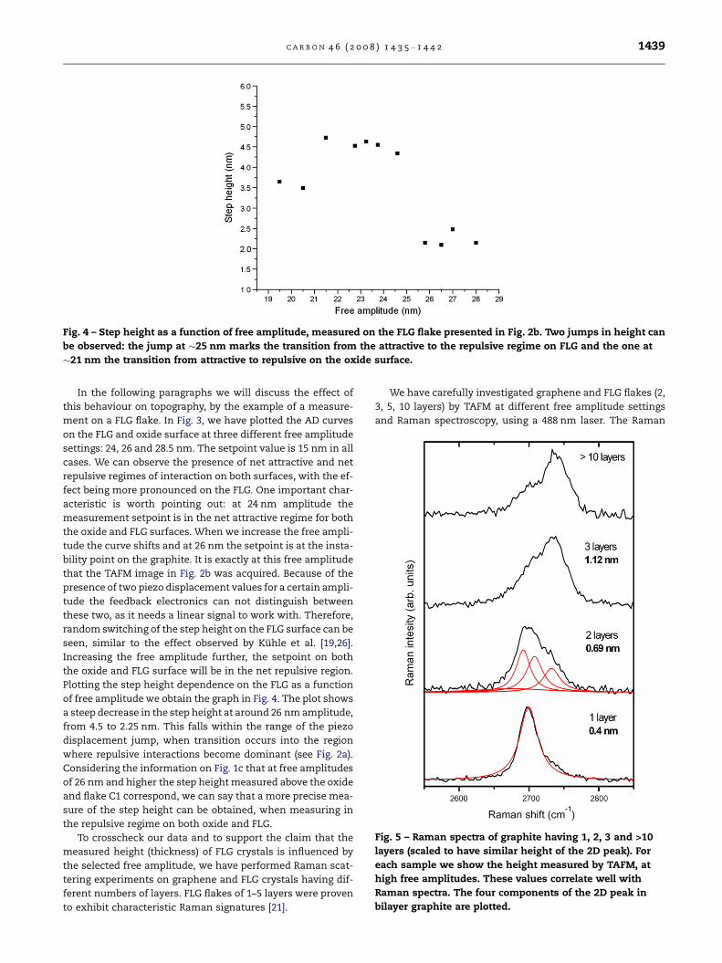
Fig. 5 – Raman spectra of graphite having 1, 2, 3 and >10
layers (scaled to have similar height of the 2D peak). For
each sample we show the height measured by TAFM, at
high free amplitudes. These values correlate well with
Raman spectra. The four components of the 2D peak in
bilayer graphite are plotted.
Fig. 4 – Step height as a function of free amplitude, measured on the FLG flake presented in Fig. 2b. Two jumps in height can
be observed: the jump at �25 nm marks the transition from the attractive to the repulsive regime on FLG and the one at
�21 nm the transition from attractive to repulsive on the oxide surface.
C A R B O N 4 6 ( 2 0 0 8 ) 1 4 3 5 – 1 4 4 2 1439
In the following paragraphs we will discuss the effect of
this behaviour on topography, by the example of a measure-
ment on a FLG flake. In Fig. 3, we have plotted the AD curves
on the FLG and oxide surface at three different free amplitude
settings: 24, 26 and 28.5 nm. The setpoint value is 15 nm in all
cases. We can observe the presence of net attractive and net
repulsive regimes of interaction on both surfaces, with the ef-
fect being more pronounced on the FLG. One important char-
acteristic is worth pointing out: at 24 nm amplitude the
measurement setpoint is in the net attractive regime for both
the oxide and FLG surfaces. When we increase the free ampli-
tude the curve shifts and at 26 nm the setpoint is at the insta-
bility point on the graphite. It is exactly at this free amplitude
that the TAFM image in Fig. 2b was acquired. Because of the
presence of two piezo displacement values for a certain ampli-
tude the feedback electronics can not distinguish between
these two, as it needs a linear signal to work with. Therefore,
random switching of the step height on the FLG surface can be
seen, similar to the effect observed by Kuhle et al. [19,26].
Increasing the free amplitude further, the setpoint on both
the oxide and FLG surface will be in the net repulsive region.
Plotting the step height dependence on the FLG as a function
of free amplitude we obtain the graph in Fig. 4. The plot shows
a steep decrease in the step height at around 26 nm amplitude,
from 4.5 to 2.25 nm. This falls within the range of the piezo
displacement jump, when transition occurs into the region
where repulsive interactions become dominant (see Fig. 2a).
Considering the information on Fig. 1c that at free amplitudes
of 26 nm and higher the step height measured above the oxide
and flake C1 correspond, we can say that a more precise mea-
sure of the step height can be obtained, when measuring in
the repulsive regime on both oxide and FLG.
To crosscheck our data and to support the claim that the
measured height (thickness) of FLG crystals is influenced by
the selected free amplitude, we have performed Raman scat-
tering experiments on graphene and FLG crystals having dif-
ferent numbers of layers. FLG flakes of 1–5 layers were proven
to exhibit characteristic Raman signatures [21].
We have carefully investigated graphene and FLG flakes (2,
3, 5, 10 layers) by TAFM at different free amplitude settings
and Raman spectroscopy, using a 488 nm laser. The Raman

1440 C A R B O N 4 6 ( 2 0 0 8 ) 1 4 3 5 – 1 4 4 2
spectra of single, bilayer and trilayer graphite are displayed in
Fig. 5. The distinct characteristics [21] of the 2D peak of graph-
ene and bilayer graphite at �2700 cm�1 are clearly identifi-
able. The Raman spectra of trilayer graphite are also clearly
distinguishable from the bulk signal. TAFM images and line-
cuts of the same FLG flakes used to acquire the Raman spec-
tra are shown in Fig. 6. Topography images acquired in the
repulsive regime, at high free amplitude settings on both
FLG and oxide surfaces fit the Raman data well. Furthermore,
the images measured using low free amplitudes show a much
larger thickness value (see Fig. 6). Where possible, we mea-
sured the thickness of folded regions (like in the case of
Fig. 1a). Such observations further support the claim that in
order to gain reliable thickness data, one needs to be using
a setpoint where the tip scans in the net repulsive regime
on both the oxide and FLG surfaces. It is worth mentioning
that true, single layer graphene crystals were frequently mea-
sured to be around 1 nm thick using free amplitudes below
the sharp drop in thickness.
In the example of the FLG layer in Fig. 2b, further decreas-
ing the free amplitude shifts the setpoint to a region where the
damping is of attractive type on both surfaces, this time with
Fig. 6 – TAFM images of the regions where the Raman spectra in
three layer (e, f) flakes (each image is 2.5 lm · 2.5 lm). The ima
two different free amplitudes, one higher (a, c, e) and another one
occurs on the FLG. In the first case (a, c, e) the setpoint is in the
case (b, d, f) imaging is in the attractive regime for FLG. Average
show the increase in thickness when measurements are not pe
the instabilities in topography appearing on the oxide (see Fig.
2c). In this case, a thickness of 3.5 nm is measured (see Fig. 4),
which is still different from the more precise thickness of
2.3 nm (about 7 layers). This goes to show that the damping
of the amplitude due to attractive forces is of a different value
for the two surfaces. Attractive forces acting on the sample
have various components: electrostatic, Van der Waals, capil-
lary or chemical forces. On mica and graphite surfaces one of
the strongest contributions to the attractive force comes from
the capillary forces, as demonstrated by Ouyang et al. [30].
This comes as no surprise, since under ambient conditions a
thin water layer is present on most surfaces. Due to the strong
hysteretic nature of the capillary force, its contribution to
oscillation damping is large [27]. According to our observa-
tions, at small free amplitude values, the tip does not even en-
ter the repulsive regime and no jump in amplitude will occur.
This is in accordance with the measurements and simulation
studies of Zitzler et al. [27], who have also demonstrated
experimentally that the free amplitude at which a jump in
the AD curves occurs is strongly dependent on the ambient
relative humidity, further proof of the fact that capillary forces
have a key role to play in cantilever damping.
Fig. 5 have been acquired, for single layer (a, b); bilayer (c, d);
ges were acquired using a constant amplitude setpoint and
lower (b, d, f) than the amplitude at which unstable imaging
repulsive regime for both oxide and FLG, while in the latter
d linecuts (inside the black markers) taken on each image
rformed in the repulsive regime.

Fig. 7 – TAFM measurements of a FLG step height at various free amplitudes (left image). CAFM measurement of the same
flake, using various deflections of the cantilever, i.e. changing the contact force (right image). Changing the contact force does
not have any effect on the step height, but the left to right and right to left scans differ by about 0.2 nm.
C A R B O N 4 6 ( 2 0 0 8 ) 1 4 3 5 – 1 4 4 2 1441
On surfaces with changing material properties, due to dif-
ferences in wettability, or more generally speaking gradients
in the attractive forces, TAFM measurements of topography
are not reliable [27]. Therefore, as seen in our experimental
results, it is advised that the TAFM measurements on graph-
ene be carried out with great care and measurement set-
points be chosen in the repulsive interaction regime, where
the damping of the cantilever is largely due to the topography
of the sample. Before measurements, amplitude–distance
curves should be acquired on both the graphene and oxide
surface and the measurement setpoint chosen accordingly.
In our measurements of FLG flakes, the difference in height
comes from the fact that the repulsive region sets in at differ-
ent free amplitude for the graphite and oxide. As the ampli-
tude setpoint crosses the jump in the AD curve unstable
imaging is observed on both the FLG and oxide. However, the
shift of the critical amplitude at which the repulsive regime
sets in and its dependence on the nature of the attractive
forces is still not fully understood. Further research in this
direction is on the way.
We have also performed CAFM measurements on our FLG
samples, which further confirm our findings. However, we
found that the difference in lateral forces on the FLG and sup-
port can introduce deviations in the thickness measured
using contact mode. This is illustrated by Fig. 7, where we
present TAFM and CAFM measurements on the same FLG
flake. The thickness of 2 nm (6 layers) measured at high free
amplitudes in tapping mode, correlates reasonably well with
the thickness measured using contact mode. However, we
have observed a difference in the thickness measured by
CAFM when changing the direction of scanning (no such ef-
fect was observed using TAFM). This suggests that differences
in lateral forces on the FLG and oxide surfaces (for example
friction) play a non-negligible role in influencing the CAFM
cantilever bending, resulting in differences in measured
thickness. Such forces are negligible in TAFM.
4. Conclusions
While performing TAFM measurements on graphene and FLG
flakes on silicon oxide substrates, special care needs to be ta-
ken to obtain more precise flake thickness data. The change
in FLG thickness described in this paper is in the order of
1 nm, which is a very large error, when working with topogra-
phy changes of less than 1 nm.
Where possible, the measurements should be performed
in the repulsive regime on both oxide and FLG surface. Either
the free amplitude or measurement setpoint should be cho-
sen in such a way as to obtain this condition. Usually the set-
point is chosen in such a way as to be as near as possible to
the free amplitude in order to minimize the forces acting on
the tip and sample, but as we have seen, this may not be
the correct setting. We believe that the variation of the re-
ported thickness of graphene among different research
groups is largely due to the unreliability of TAFM measure-
ments in the attractive regime. It is worth noting here that
during our measurements at high free amplitude and low set-
point settings, no damage to either the sample or tip were
encountered.
Our work sheds some light on how a more precise esti-
mate of the number of layers in a FLG crystal can be obtained.
However, the number of layers should be compared to data
obtained by other methods as well, to support the AFM data.
Furthermore, additional experimental work and computer
simulation needs to be done, to determine the cause of the
shift in the instability point on the AD curves and the nature
of the attractive forces on the sample.
Acknowledgements
The present work was financially supported by Hungarian
Scientific Research Fund OTKA-NKTH K67793, OTKA-NKTH
NI67702 and OTKA-NKTH 67842 Grants.

1442 C A R B O N 4 6 ( 2 0 0 8 ) 1 4 3 5 – 1 4 4 2
R E F E R E N C E S
[1] Wallace PR. The band theory of graphite. Phys Rev1947;71:622–34.
[2] Novoselov KS, Geim AK, Morozov SV, Jiang D, Zhang Y,Dubonos V, et al. Electric field effect in atomically thincarbon films. Science 2004;306:666–9.
[3] Novoselov KS, Jiang D, Schedin F, Booth TJ, Khotkevich VV,Morozov SV, et al. Two-dimensional atomic crystals. ProcNatl Acad Sci USA 2005;102:10451–3.
[4] Landau LD, Lifshitz EM. Statistical physics, part I. Oxford:Pergamon Press; 1980.
[5] Mermin ND. Crystalline order in two dimensions. Phys Rev1968;176:250–4.
[6] Katsnelson MI. Graphene: carbon in two dimensions. MaterToday 2007;10:20–7.
[7] Novoselov KS, McCann E, Morozov SV, Fal’Ko VI, KatsnelsonMI, Zeitler U, et al. Unconventional quantum Hall effect andBerry’s phase of 2p in bilayer graphene. Nat Phys2006;2:177–80.
[8] Heersche, Jarillo-Herrero P, Oostinga JB, Vandersypen LMK,Morpurgo AF. Nature 2007;446:56–9.
[9] Stolyarova E, Rim KT, Ryu S, Maultzsch J, Kim P, Brus LE, et al.High-resolution scanning tunneling microscopy imaging ofmesoscopic graphene sheets on an insulating surface. ProcNatl Acad Sci USA 2007;104:9209–12.
[10] Schedin F, Geim AK, Morozov SV, Hill EW, Blake P, KatsnelsonMI, et al. Detection of individual gas molecules adsorbed ongraphene. Nat Mater 2007;6:652–5.
[11] Dikin DA, Stankovich S, Zimney EJ, Piner RD, Dommett GHB,Evmenenko G, et al. Preparation and characterization ofgraphene oxide paper. Nature 2007;448:457–60.
[12] Novoselov KS, Geim AK, Morozov SV, Jiang D, Katsnelson MI,Grigorieva IV, et al. Two-dimensional gas of massless Diracfermions in graphene. Nature 2005;438:197–200.
[13] Roddaro S, Pingue P, Piazza V, Pellegrini V, Beltram F. Theoptical visibility of graphene: interference colors of ultrathingraphite on SiO2. Nano Lett 2007;7:2707–10.
[14] Blake P, Hill EW, Castro Neto AH, Novoselov KS, Jiang D, YangR, et al. Making graphene visible. Appl Phys Lett2007;91:063124.
[15] Chen Z, Lin Y-M, Rooks MJ, Avouris P. Graphene nano-ribbonelectronics. Physica E 2007;40:228–32.
[16] Sidorov AN, Yazdanpanah MM, Jalilian R, Jouseph P, Cohn RW,Sumanasekera GU. Electrostatic deposition of graphene.Nanotechnology 2007;18:135301.
[17] Mechler A, Kopniczky J, Kokavecz J, Hoel A, Granqvist C-G,et al. Anomalies in nanostructure size measurements byAFM. Phys Rev B 2005;72:125407.
[18] Mechler A, Kokavecz J, Heszler P, Lal R. Surface energy mapsof nanostructures: atomic force microscopy and numericalsimulation study. Appl Phys Lett 2003;82:3740–2.
[19] Kuhle A, Sørensen AH, Zandbergen JB, Bohr J. Contrastartifacts in tapping tip atomic force microscopy. Appl Phys A1998;66:S329–32.
[20] Gupta A, Chen G, Joshi P, Tadigadapa S, Eklund PC. Ramanscattering from high-frequency phonons in supportedn-graphene layer films. Nano Lett 2006;6:2667–73.
[21] Ferrari C, Meyer JC, Scardaci V, Casiraghi C, Lazzeri M, MauriF, et al. Raman spectrum of graphene and graphene layers.Phys Rev Lett 2006;97:187401.
[22] Graf D, Molitor F, Ensslin K, Stampfer C, Jungen A, Hierold C,et al. Spatially resolved Raman spectroscopy of single- andfew-layer graphene. Nano Lett 2007;7:238–42.
[23] Casiraghi C, Hartschuh A, Lidorikis E, Qian H, HarutyunyanH, Gokus T, et al. Rayleigh imaging of graphene andgraphene layers. Nano Lett 2007;7:2711–7.
[24] Ni ZH, Wang HM, Kasim J, Fan HM, Yu T, Wu YH, et al.Graphene thickness determination using reflection andcontrast spectroscopy. Nano Lett 2007;7:2758–63.
[25] Jung I, Pelton M, Piner R, Dikin DA, Stankovich S,Watcharotone S, et al. Simple approach for high-contrastoptical imaging and characterization of graphene-basedsheets. Nano Lett 2007;7:3569–75.
[26] Kuhle A, Sorensen AH, Bohr J. Role of attractive forces intapping tip force microscopy. J Appl Phys 1997;81:6562–9.
[27] Zitzler L, Herminghaus S, Mugele F. Capillary forces in tappingmode atomic force microscopy. Phys Rev B 2002;66:155436.
[28] Anczykowski B, Kruger D, Babcock KL, Fuchs H. Basicproperties of dynamic force spectroscopy with the scanningforce microscope in experiment and simulation.Ultramicroscopy 1996;66:251–9.
[29] Garcia R, San Paulo A. Attractive and repulsive tip-sampleinteraction regimes in tapping-mode atomic forcemicroscopy. Phys Rev B 1999;60:4961–7.
[30] Ouyang Q, Ishida K, Okada K. Investigation of micro-adhesionby atomic force microscopy. Appl Surf Sci 2001;169–170:644–8.