Embed Size (px)
DESCRIPTION
Antena Circuit Design
Citation preview

AN710
Antenna Circuit Design for RFID Applications
INTRODUCTION
Passive RFID tags utilize an induced antenna coil
voltage for operation. This induced AC voltage is
rectified to provide a voltage source for the device. As
the DC voltage reaches a certain level, the device
starts operating. By providing an energizing RF signal,
a reader can communicate with a remotely located
device that has no external power source such as a
battery. Since the energizing and communication
between the reader and tag is accomplished through
antenna coils, it is important that the device must be
equipped with a proper antenna circuit for successful
RFID applications.
An RF signal can be radiated effectively if the linear
dimension of the antenna is comparable with the
wavelength of the operating frequency. However, the
wavelength at 13.56 MHz is 22.12 meters. Therefore,
it is difficult to form a true antenna for most RFID appli-
cations. Alternatively, a small loop antenna circuit that
is resonating at the frequency is used. A current
flowing into the coil radiates a near-field magnetic field
that falls off with r-3. This type of antenna is called a
magnetic dipole antenna.
For 13.56 MHz passive tag applications, a few
microhenries of inductance and a few hundred pF of
resonant capacitor are typically used. The voltage
transfer between the reader and tag coils is accom-
plished through inductive coupling between the two
coils. As in a typical transformer, where a voltage in the
primary coil transfers to the secondary coil, the voltage
in the reader antenna coil is transferred to the tag
antenna coil and vice versa. The efficiency of the
voltage transfer can be increased significantly with high
Q circuits.
This section is written for RF coil designers and RFID
system engineers. It reviews basic electromagnetic
theories on antenna coils, a procedure for coil design,
calculation and measurement of inductance, an
antenna tuning method, and read range in RFID
applications.
REVIEW OF A BASIC THEORY FOR
RFID ANTENNA DESIGN
Current and Magnetic Fields
Ampere’s law states that current flowing in a conductor
produces a magnetic field around the conductor. The
magnetic field produced by a current element, as
shown in Figure 1, on a round conductor (wire) with a
finite length is given by:
EQUATION 1:
where:
In a special case with an infinitely long wire where:
Equation 1 can be rewritten as:
EQUATION 2:
FIGURE 1: CALCULATION OF MAGNETIC
FIELD B AT LOCATION P DUE TO
CURRENT I ON A STRAIGHT
CONDUCTING WIRE
Author: Youbok Lee, Ph.D.
Microchip Technology Inc.
I = current
r = distance from the center of wire
µ0 = permeability of free space and given
as 4 π x 10-7 (Henry/meter)
α1 = -180°
α2 = 0°
Bφ
µoI
4πr--------- α2cos α1cos–( )= Weber m
2⁄( )
Bφ
µoI
2πr---------= Weber m
2⁄( )
Wire
dL
I
r0 B (into the page)
P
R
α2
α
α1
Ζ
X
2003 Microchip Technology Inc. DS00710C-page 1

AN710
The magnetic field produced by a circular loop antenna
is given by:
EQUATION 3:
where
The above equation indicates that the magnetic field
strength decays with 1/r3. A graphical demonstration is
shown in Figure 3. It has maximum amplitude in the
plane of the loop and directly proportional to both the
current and the number of turns, N.
Equation 3 is often used to calculate the ampere-turn
requirement for read range. A few examples that
calculate the ampere-turns and the field intensity
necessary to power the tag will be given in the following
sections.
FIGURE 2: CALCULATION OF MAGNETIC
FIELD B AT LOCATION P DUE TO
CURRENT I ON THE LOOP
FIGURE 3: DECAYING OF THE MAGNETIC
FIELD B VS. DISTANCE r
I = current
radius of loop
distance from the center of loop
a =
r =
µ0 = permeability of free space and given as
4 π x 10-7 (Henry/meter)
Bz
µoINa2
2 a2
r2
+( )3 2⁄
----------------------------------=
µoINa2
2------------------
1
r3-----
= for r2>>a
2 α
R
ry
Icoil
Bz
P
z
a
X
V Vo ωtsin=
r
r-3
B
DS00710C-page 2 2003 Microchip Technology Inc.

AN710
INDUCED VOLTAGE IN AN ANTENNA
COIL
Faraday’s law states that a time-varying magnetic field
through a surface bounded by a closed path induces a
voltage around the loop.
Figure 4 shows a simple geometry of an RFID applica-
tion. When the tag and reader antennas are in close
proximity, the time-varying magnetic field B that is
produced by a reader antenna coil induces a voltage
(called electromotive force or simply EMF) in the closed
tag antenna coil. The induced voltage in the coil causes
a flow of current on the coil. This is called Faraday’s
law. The induced voltage on the tag antenna coil is
equal to the time rate of change of the magnetic flux Ψ.
EQUATION 4:
where:
The negative sign shows that the induced voltage acts
in such a way as to oppose the magnetic flux producing
it. This is known as Lenz’s law and it emphasizes the
fact that the direction of current flow in the circuit is
such that the induced magnetic field produced by the
induced current will oppose the original magnetic field.
The magnetic flux Ψ in Equation 4 is the total magnetic
field B that is passing through the entire surface of the
antenna coil, and found by:
EQUATION 5:
where:
The presentation of inner product of two vectors in
Equation 5 suggests that the total magnetic flux ψ that
is passing through the antenna coil is affected by an
orientation of the antenna coils. The inner product of
two vectors becomes minimized when the cosine angle
between the two are 90 degrees, or the two (B field and
the surface of coil) are perpendicular to each other and
maximized when the cosine angle is 0 degrees.
The maximum magnetic flux that is passing through the
tag coil is obtained when the two coils (reader coil and
tag coil) are placed in parallel with respect to each
other. This condition results in maximum induced volt-
age in the tag coil and also maximum read range. The
inner product expression in Equation 5 also can be
expressed in terms of a mutual coupling between the
reader and tag coils. The mutual coupling between the
two coils is maximized in the above condition.
FIGURE 4: A BASIC CONFIGURATION OF READER AND TAG ANTENNAS IN RFID APPLICATIONS
N = number of turns in the antenna coil
Ψ = magnetic flux through each turn
V Ndψdt-------–=
B = magnetic field given in Equation 2
S = surface area of the coil
• = inner product (cosine angle between two
vectors) of vectors B and surface area S
Note: Both magnetic field B and surface S
are vector quantities.
ψ B· Sd∫=
Tag Coil V = V0sin(ωt)
Tag
B = B0sin(ωt)
Reader Coil
I = I0sin(ωt)
Tuning CircuitReader
Electronics
2003 Microchip Technology Inc. DS00710C-page 3

AN710
Using Equations 3 and 5, Equation 4 can be rewritten
as:
EQUATION 6:
where:
EQUATION 7:
The above equation is equivalent to a voltage transfor-
mation in typical transformer applications. The current
flow in the primary coil produces a magnetic flux that
causes a voltage induction at the secondary coil.
As shown in Equation 6, the tag coil voltage is largely
dependent on the mutual inductance between the two
coils. The mutual inductance is a function of coil
geometry and the spacing between them. The induced
voltage in the tag coil decreases with r-3. Therefore, the
read range also decreases in the same way.
From Equations 4 and 5, a generalized expression for
induced voltage Vo in a tuned loop coil is given by:
EQUATION 8:
where:
In the above equation, the quality factor Q is a measure
of the selectivity of the frequency of the interest. The Q
will be defined in Equations 43 through 59.
FIGURE 5: ORIENTATION DEPENDENCY OF
THE TAG ANTENNA
The induced voltage developed across the loop
antenna coil is a function of the angle of the arrival
signal. The induced voltage is maximized when the
antenna coil is placed in parallel with the incoming
signal where α = 0.
V = voltage in the tag coil
i1 = current on the reader coil
a = radius of the reader coil
b = radius of tag coil
r = distance between the two coils
M = mutual inductance between the tag
and reader coils, and given by:
V N2 dΨ21
dt-------------– N2
d
dt----- B∫ Sd⋅( )–= =
µoN1N2a
2πb
2( )
2 a2
r2
+( )3 2⁄
----------------------------------------- di1
dt-------–=
M di1
dt-------–=
N2 d
dt-----
µoi1N1a2
2 a2
r2
+( )3 2⁄
----------------------------------· Sd∫–=
MµoπN1N2 ab( )
2
2 a2
r2
+( )3 2⁄
--------------------------------------=
f = frequency of the arrival signal
N = number of turns of coil in the loop
S = area of the loop in square meters (m2)
Q = quality factor of circuit
Βo = strength of the arrival signal
α = angle of arrival of the signal
V0 2πfNSQBo αcos=
Tag
B-field
a
DS00710C-page 4 2003 Microchip Technology Inc.

AN710
EXAMPLE 1: CALCULATION OF B-FIELD IN
A TAG COIL
EXAMPLE 2: NUMBER OF TURNS AND
CURRENT (AMPERE-TURNS)
EXAMPLE 3: OPTIMUM COIL DIAMETER
OF THE READER COIL
The above result shows a relationship between the
read range versus optimum coil diameter. The optimum
coil diameter is found as:
EQUATION 12:
where:
The result indicates that the optimum loop radius, a, is
1.414 times the demanded read range r.
The MCRF355 device turns on when the antenna
coil develops 4 VPP across it. This voltage is rectified
and the device starts to operate when it reaches 2.4
VDC. The B-field to induce a 4 VPP coil voltage with
an ISO standard 7810 card size (85.6 x 54 x 0.76
mm) is calculated from the coil voltage equation
using Equation 8.
EQUATION 9:
and
where the following parameters are used in the
above calculation:
Tag coil size = (85.6 x 54) mm2 (ISO card
size) = 0.0046224 m2
Frequency = 13.56 MHz
Number of turns = 4
Q of tag antenna
coil
= 40
AC coil voltage to
turn on the tag
= 4 VPP
cosα = 1 (normal direction, α = 0).
Vo 2πfNSQBo α 4=cos=
Bo 4 2( )⁄
2πfNSQ αcos----------------------------------- 0.0449== µwbm
2–( )
Assuming that the reader should provide a read
range of 15 inches (38.1 cm) for the tag given in the
previous example, the current and number of turns
of a reader antenna coil is calculated from
Equation 3:
EQUATION 10:
The above result indicates that it needs a 430 mA
for 1 turn coil, and 215 mA for 2-turn coil.
NI( )rms
2Bz a2
r2
+( )
µa2
-------------------------------
3 2⁄
=
2 0.0449 106–
×( ) 0.12
0.38( )2
+( )
4π 107–
×( ) 0.12
( )---------------------------------------------------------------------------------------
3 2⁄
=
0.43 ampere - turns( )=
a = radius of coil
r = read range.
An optimum coil diameter that requires the minimum
number of ampere-turns for a particular read range
can be found from Equation 3 such as:
EQUATION 11:
NI Ka
2r2
+( )
3
2---
a2
-------------------------=
K2Bz
µo
---------=where:
d NI( )da
-------------- K 3 2⁄ a
2r2
+( )1 2⁄
2a3
( ) 2a a2
r2
+( )3 2⁄
–
a4
----------------------------------------------------------------------------------------------------=
By taking derivative with respect to the radius a,
Ka
22r
2–( ) a
2r2
+( )1 2⁄
a3
--------------------------------------------------------=
The above equation becomes minimized when:
a 2= r
2003 Microchip Technology Inc. DS00710C-page 5

AN710
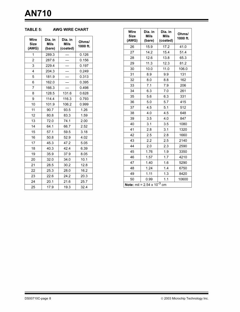
WIRE TYPES AND OHMIC LOSSES
DC Resistance of Conductor and Wire
Types
The diameter of electrical wire is expressed as the
American Wire Gauge (AWG) number. The gauge
number is inversely proportional to diameter, and the
diameter is roughly doubled every six wire gauges. The
wire with a smaller diameter has a higher DC
resistance. The DC resistance for a conductor with a
uniform cross-sectional area is found by:
EQUATION 13: DC Resistance of Wire
where:
For a The resistance must be kept small as possible for
higher Q of antenna circuit. For this reason, a larger
diameter coil as possible must be chosen for the RFID
circuit. Table 5 shows the diameter for bare and
enamel-coated wires, and DC resistance.
AC Resistance of Conductor
At DC, charge carriers are evenly distributed through
the entire cross section of a wire. As the frequency
increases, the magnetic field is increased at the center
of the inductor. Therefore, the reactance near the
center of the wire increases. This results in higher
impedance to the current density in the region. There-
fore, the charge moves away from the center of the
wire and towards the edge of the wire. As a result, the
current density decreases in the center of the wire and
increases near the edge of the wire. This is called a
skin effect. The depth into the conductor at which the
current density falls to 1/e, or 37% (= 0.3679) of its
value along the surface, is known as the skin depth and
is a function of the frequency and the permeability and
conductivity of the medium. The net result of skin effect
is an effective decrease in the cross sectional area of
the conductor. Therefore, a net increase in the AC
resistance of the wire. The skin depth is given by:
EQUATION 14:
where:
EXAMPLE 4:
As shown in Example 4, 63% of the RF current flowing
in a copper wire will flow within a distance of 0.018 mm
of the outer edge of wire for 13.56 MHz and 0.187 mm
for 125 kHz.
The wire resistance increases with frequency, and the
resistance due to the skin depth is called an AC
resistance. An approximated formula for the AC
resistance is given by:
l = total length of the wire
σ = conductivity of the wire (mho/m)
S = cross-sectional area = π r2
a = radius of wire
RDC
l
σS------
l
σπa2
-------------= = Ω( )
f = frequency
µ = permeability (F/m) = µοµr
µo = Permeability of air = 4 π x 10-7 (h/m)
µr = 1 for Copper, Aluminum, Gold, etc
= 4000 for pure Iron
σ = Conductivity of the material (mho/m)
= 5.8 x 10⁷ (mho/m) for Copper
= 3.82 x 10⁷ (mho/m) for Aluminum
= 4.1 x 10⁷ (mho/m) for Gold
= 6.1 x 10⁷ (mho/m) for Silver
= 1.5 x 10⁷ (mho/m) for Brass
δ1
πfµσ-----------------=
The skin depth for a copper wire at 13.56 MHz and
125 kHz can be calculated as:
EQUATION 15:
δ1
πf 4π 107–
×( ) 5.8 107
×( )------------------------------------------------------------------------=
0.0661
f------------------= m( )
0.018= mm( ) for 13.56 MHz
0.187= mm( ) for 125 kHz
DS00710C-page 6 2003 Microchip Technology Inc.

AN710
EQUATION 16:
The AC resistance increases with the square root of the
operating frequency.
For the conductor etched on dielectric, substrate is
given by:
EQUATION 17:
where w is the width and t is the thickness of the
conductor.
Resistance of Conductor with Low
Frequency Approximation
When the skin depth is almost comparable to the radius
of conductor, the resistance can be obtained with a low
frequency approximation[5]:
EQUATION 18:
The first term of the above equation is the DC
resistance, and the second term represents the AC
resistance.
l
2a------
fµπσ-------= Ω( )
Rac
l
σAactive
--------------------l
2πaδσ-----------------≈= Ω( )
Rdc( )a
2δ------= Ω( )
where the skin depth area on the conductor is,
Aactive 2πaδ≈
Rac
l
σ w t+( )δ------------------------
l
w t+( )----------------
πfµσ---------= = Ω( )
Rlow freq
l
σπa2
------------- 11
48------
a
δ---
2+≈ Ω( )
2003 Microchip Technology Inc. DS00710C-page 7
AN710
TABLE 5: AWG WIRE CHART
Wire
Size
(AWG)
Dia. in
Mils
(bare)
Dia. in
Mils
(coated)
Ohms/
1000 ft.
1 289.3 — 0.126
2 287.6 — 0.156
3 229.4 — 0.197
4 204.3 — 0.249
5 181.9 — 0.313
6 162.0 — 0.395
7 166.3 — 0.498
8 128.5 131.6 0.628
9 114.4 116.3 0.793
10 101.9 106.2 0.999
11 90.7 93.5 1.26
12 80.8 83.3 1.59
13 72.0 74.1 2.00
14 64.1 66.7 2.52
15 57.1 59.5 3.18
16 50.8 52.9 4.02
17 45.3 47.2 5.05
18 40.3 42.4 6.39
19 35.9 37.9 8.05
20 32.0 34.0 10.1
21 28.5 30.2 12.8
22 25.3 28.0 16.2
23 22.6 24.2 20.3
24 20.1 21.6 25.7
25 17.9 19.3 32.4
26 15.9 17.2 41.0
27 14.2 15.4 51.4
28 12.6 13.8 65.3
29 11.3 12.3 81.2
30 10.0 11.0 106.0
31 8.9 9.9 131
32 8.0 8.8 162
33 7.1 7.9 206
34 6.3 7.0 261
35 5.6 6.3 331
36 5.0 5.7 415
37 4.5 5.1 512
38 4.0 4.5 648
39 3.5 4.0 847
40 3.1 3.5 1080
41 2.8 3.1 1320
42 2.5 2.8 1660
43 2.2 2.5 2140
44 2.0 2.3 2590
45 1.76 1.9 3350
46 1.57 1.7 4210
47 1.40 1.6 5290
48 1.24 1.4 6750
49 1.11 1.3 8420
50 0.99 1.1 10600
Note: mil = 2.54 x 10⁻³ cm
Wire
Size
(AWG)
Dia. in
Mils
(bare)
Dia. in
Mils
(coated)
Ohms/
1000 ft.
DS00710C-page 8 2003 Microchip Technology Inc.

AN710
INDUCTANCE OF VARIOUS
ANTENNA COILS
An electric current element that flows through a
conductor produces a magnetic field. This time-varying
magnetic field is capable of producing a flow of current
through another conductor – this is called inductance.
The inductance L depends on the physical characteris-
tics of the conductor. A coil has more inductance than
a straight wire of the same material, and a coil with
more turns has more inductance than a coil with fewer
turns. The inductance L of inductor is defined as the
ratio of the total magnetic flux linkage to the current Ιthrough the inductor:
EQUATION 19:
where:
For a coil with multiple turns, the inductance is greater
as the spacing between turns becomes smaller. There-
fore, the tag antenna coil that has to be formed in a
limited space often needs a multilayer winding to
reduce the number of turns.
Calculation of Inductance
Inductance of the coil can be calculated in many
different ways. Some are readily available from
references[1-7]. It must be remembered that for RF
coils the actual resulting inductance may differ from the
calculated true result because of distributed capaci-
tance. For that reason, inductance calculations are
generally used only for a starting point in the final
design.
INDUCTANCE OF A STRAIGHT WOUND WIRE
The inductance of a straight wound wire shown in
Figure 1 is given by:
EQUATION 20:
where:
EXAMPLE 6: INDUCTANCE CALCULATION
FOR A STRAIGHT WIRE:
N = number of turns
I = current
Ψ = the magnetic flux
LNψ
I--------= (Henry)
l and a = length and radius of wire in cm,
respectively.
L 0.002l loge
2l
a-----
3
4---–= µH( )
The inductance of a wire with 10 feet (304.8cm) long
and 2 mm in diameter is calculated as follows:
EQUATION 21:
L 0.002 304.8( ) 2 304.8( )0.1
----------------------- ln
3
4---– =
0.60967 7.965( )=
4.855 µH( )=
2003 Microchip Technology Inc. DS00710C-page 9

AN710
INDUCTANCE OF A SINGLE TURN CIRCULAR
COIL
The inductance of a single turn circular coil shown in
Figure 6 can be calculated by:
FIGURE 6: A CIRCULAR COIL WITH SINGLE
TURN
EQUATION 22:
where:
INDUCTANCE OF AN N-TURN SINGLE LAYER
CIRCULAR COIL
FIGURE 7: A CIRCULAR COIL WITH SINGLE
TURN
EQUATION 23:
where:
INDUCTANCE OF N-TURN MULTILAYER
CIRCULAR COIL
FIGURE 8: N-TURN MULTILAYER
CIRCULAR COIL
Figure 8 shows an N-turn inductor of circular coil with
multilayer. Its inductance is calculated by:
EQUATION 24:
where:
a = mean radius of loop in (cm)
d = diameter of wire in (cm)
N = number of turns
l = length in cm
a = the radius of coil in cm
X d
a
L 0.01257 a( ) 2.303log1016a
d---------- 2–
= µH( )
a
l
LaN( )
2
22.9a 25.4l+-----------------------------------= µH( )
a = average radius of the coil in cm
N = number of turns
b = winding thickness in cm
h = winding height in cm
X
b
a
N-turns coil
a
b
h
L0.31 aN( )
2
6a 9h 10b+ +------------------------------------= µH( )
DS00710C-page 10 2003 Microchip Technology Inc.

AN710
INDUCTANCE OF SPIRAL WOUND COIL WITH
SINGLE LAYER
The inductance of a spiral inductor is calculated by:
EQUATION 25:
FIGURE 9: A SPIRAL COIL
where:
INDUCTANCE OF N-TURN SQUARE LOOP
COIL WITH MULTILAYER
Inductance of a multilayer square loop coil is calculated
by:
EQUATION 26:
where:
FIGURE 10: N-TURN SQUARE LOOP COIL
WITH MULTILAYER
a = (ri + ro)/2
b = ro – ri
ri = Inner radius of the spiral
ro = Outer radius of the spiral
Note: All dimensions are in cm
L0.3937( ) aN( )
2
8a 11b+--------------------------------------= µH( )
a
bri
ro
N = number of turns
a = side of square measured to the center of
the rectangular cross section of winding
b = winding length
c = winding depth as shown in Figure 10
Note: All dimensions are in cm
L 0.008aN2
2.303log10
a
b c+------------ 0.2235
b c+
a------------ 0.726+ +
µH( )=
(a) Top View (b) Cross Sectional View
a
b
c
a
2003 Microchip Technology Inc. DS00710C-page 11

AN710
INDUCTANCE OF N-TURN RECTANGULAR
COIL WITH MULTILAYER
Inductance of a multilayer rectangular loop coil is
calculated by:
EQUATION 27:
where:
FIGURE 11: N-TURN SQUARE LOOP COIL
WITH MULTILAYER
INDUCTANCE OF THIN FILM INDUCTOR
WITH A RECTANGULAR CROSS SECTION
Inductance of a conductor with rectangular cross
section as shown in Figure 12 is calculated as:
FIGURE 12: A STRAIGHT THIN FILM
INDUCTOR
EQUATION 28:
where:
N = number of turns
C = x + y + 2h
x = width of coil
y = length of coil
b = width of cross section
h = height (coil build up) of cross section
Note: All dimensions are in cm
L0.0276 CN( )
2
1.908C 9b 10h+ +------------------------------------------------ µH( )=
(a) Top View
(b) Cross Sectional View
b
y
h
x
w = width in cm
t = thickness in cm
l = length of conductor in cm
t
w
l
L 0.002l2l
w t+------------
0.50049w t+
3l------------+ +ln
= µH( )
DS00710C-page 12 2003 Microchip Technology Inc.

AN710
INDUCTANCE OF A FLAT SQUARE COIL
Inductance of a flat square coil of rectangular cross
section with N turns is calculated by[2]:
EQUATION 29:
where:
FIGURE 13: SQUARE LOOP INDUCTOR WITH
A RECTANGULAR CROSS
SECTION
L 0.0467aN2
log10 2a2
t w+------------
log10 2.414a( )–
0.02032aN2
0.9140.2235
a------------------ t w+( )+
+=
L = in µH
a = side length in inches
t = thickness in inches
w = width in inches
N = total number of turns
wa
2003 Microchip Technology Inc. DS00710C-page 13

AN710
EXAMPLE ON ONE TURN READER ANTENNA
If reader antenna is made of a rectangular loop
composed of a thin wire or a thin plate element, its
inductance can be calculated by the following simple
formula [5]:
FIGURE 14: ONE TURN READER ANTENNA
EQUATION 30:
where
units are all in cm, and a = radius of wire in cm.
Example with dimension:
One-turn rectangular shape with la = 18.887 cm, lb =
25.4 cm, width a = 0.254 cm gives 653 (nH) using the
above equation.
2 a
la
lb
[ ] )()(2)(
2ln
)(
2ln4 nHllla
lla
Al
lla
AlL
bac
ca
a
cb
b
+−++
++
+=
lc la2
lb2
+=
A la lb×=
DS00710C-page 14 2003 Microchip Technology Inc.

AN710
INDUCTANCE OF N-TURN PLANAR SPIRAL
COIL
Inductance of planar structure is well calculated in
Reference [4]. Consider an inductor made of straight
segments as shown in Figure 15. The inductance is the
sum of self inductances and mutual inductances[4]:
EQUATION 31:
where:
The mutual inductance is the inductance that is
resulted from the magnetic fields produced by adjacent
conductors. The mutual inductance is positive when
the directions of current on conductors are in the same
direction, and negative when the directions of currents
are opposite directions. The mutual inductance
between two parallel conductors is a function of the
length of the conductors and of the geometric mean
distance between them. The mutual inductance of two
conductors is calculated by:
EQUATION 32:
where l is the length of conductor in centimeter. F is the
mutual inductance parameter and calculated as:
EQUATION 33:
where d is the geometric mean distance between two
conductors, which is approximately equal to the
distance between the track center of the conductors.
Let us consider the two conductor segments shown in
Figure 15:
FIGURE 15: TWO CONDUCTOR SEGMENTS FOR
MUTUAL INDUCTANCE
CALCULATION
j and k in the above figure are indices of conductor, and
p and q are the indices of the length for the difference
in the length of the two conductors.
The above configuration (with partial segments) occurs
between conductors in multiple turn spiral inductor. The
mutual inductance of conductors j and k in the above
configuration is:
EQUATION 34:
If the length of l1 and l2 are the same (l1 = l2), then
Equation 34 (d) is used. Each mutual inductance term
in the above equation is calculated as follows by using
Equations 33 and 34:
EQUATION 35:
The following examples shows how to use the above
formulas to calculate the inductance of a 4-turn
rectangular spiral inductor.
LT = Total Inductance
Lo = Sum of self inductances of all straight
segments
M+ = Sum of positive mutual inductances
M- = Sum of negative mutual inductances
LT Lo M+
– M–
–= µH( )
M 2lF= nH( )
Fl
d---
1l
d---
2+
1 2⁄+
ln 1l
d---
2+
1 2⁄–
d
l---
+=
l1
l2
d
p q
j
k
Mj k,
1
2--- Mk p+
Mk q++( ) Mp Mq+( )– =
1
2--- Mj Mk+( ) Mq– = for p 0=
1
2--- Mj Mk+( ) Mp– = for q 0=
Mk p+Mp–= for p q=
Mk= for p q 0= =
(a)
(b)
(c)
(d)
Mk p+2lk p+
Fk p+=
where
Fk p+
lk p+
dj k,
-------------
1lk p+
dj k,
------------- 2
+
1 2⁄+
ln=
1d
j k,lk p+
------------- 2
+
1 2⁄–
dj k,
lk p+
-------------
+
2003 Microchip Technology Inc. DS00710C-page 15

AN710
EXAMPLE 7: INDUCTANCE OF
RECTANGULAR PLANAR
SPIRAL INDUCTOR
1, 2, 3, ... ,16 are indices of conductor. For four full turn
inductor, there are 16 straight segments. s is the spac-
ing between conductor, and δ (= s + w) is the distance
of track centers between two adjacent conductors. l1is the length of conductor 1, l2 is the length of conductor
2, and so on. The length of conductor segments are:
l3 = l1 , l4 = l2 - δ , l5 = l1 - δ , l6 = l4 - δ ,
l7 = l5 - δ , l8 = l6 - δ , l9 = l7 - δ ,
l10 = l8 - δ , l11 = l9 - δ , l12 = l10 -δ ,
l13 = l11 - δ , l14 = l12 - δ , l15 = l13 - δ ,
l16 = l14 - δ
The total inductance of the coil is equal to the sum of
the self inductance of each straight segment (L0 = L1 +
L2 + L3 + L4 +.....+ L16) plus all the mutual inductances
between these segments as shown in Equation 31.
The self inductance is calculated by Equation (28), and
the mutual inductances are calculated by Equations
(32) - (34).
For the four-turn spiral, there are both positive and
negative mutual inductances. The positive mutual
inductance (M+) is the mutual inductance between
conductors that have the same current direction. For
example, the current on segments 1 and 5 are in the
same direction. Therefore, the mutual inductance
between the two conductor segments is positive. On
the other hand, the currents on segments 1 and 15 are
in the opposite direction. Therefore, the mutual induc-
tance between conductors 1 and 15 is negative term.
The mutual inductance is maximized if the two
segments are in parallel, and minimum if they are
placed in orthogonal (in 90 degrees). Therefore the
mutual inductance between segments 1 and 2, 1 and 6,
1 and 10, 1 and 14, etc, are negligible in calculation.
In Example 7, the total positive mutual inductance
terms are:
EQUATION 36:
The total negative mutual inductance terms are:
EQUATION 37:
See Appendix A for calculation of each individual
mutual inductance term in Equations (36) - (37).
1
2
3
4
5
9
13
6 10 14
7
11
15
81216
s δ
l1
w
l4l2
l3
M+
2 M1 5, M1 9, M1 13,+ +( )=
+2 M5 9, M5 13, M9 13,+ +( )
+2 M3 7, M3 11, M3 15,+ +( )
+2 M7 11, M7 15, M11 15,+ +( )
+2 M2 6, M2 10, M2 14,+ +( )
+2 M6 10, M6 14, M10 14,+ +( )
+2 M4 8, M4 12, M4 16,+ +( )
+2 M8 12, M8 16, M12 16,+ +( )
M–
2 M1 3, M1 7, M1 11, M1 15,+ + +( )=
+2 M5 3, M5 7, M5 11, M5 15,+ + +( )
+2 M9 3, M9 7, M9 11, M9 15,+ + +( )
+2 M2 4, M2 8, M2 12, M2 16,+ + +( )
+2 M6 4, M6 8, M6 12, M6 16,+ + +( )
+2 M10 4, M10 8, M10 12, M10 16,+ + +( )
+2 M14 4, M14 8, M14 12, M14 16,+ + +( )
+2 M13 15, M13 11, M13 7, M13 3,+ + +( )
DS00710C-page 16 2003 Microchip Technology Inc.

AN710
EXAMPLE 8: INDUCTANCE CALCULATION
INCLUDING MUTUAL
INDUCTANCE TERMS FOR A
RECTANGULAR SHAPED ONE
TURN READER ANTENNA
In the one turn rectangular shape inductor, there are
four sides. Because of the gap, there are a total of 5
conductor segments. In one-turn inductor, the direction
of current on each conductor segment is all opposite
directions to each other. For example, the direction of
current on segment 2 and 4, 1 and 3, 1’ and 3 are
opposite. There is no conductor segments that have
the same current direction. Therefore, there is no
positive mutual inductance.
From Equation 31, the total inductance is:
EQUATION 38:
Let us calculate the Inductance of one turn loop
etched antenna on PCB board for reader antenna
(for example, the MCRF450 reader antenna in the
DV103006 development kit) with the following
parameters:
l2 = l4 = 10” = 25.4 cm
l3 = 7.436” = 18.887 cm
l1 = l1’ = 3” = 7.62
gap = 1.4536” = 3.692 cm
trace width (w) = 0.508 cm
trace thickness (t) = 0.0001 cm
Gap
l1
l2
l3
l4
l1’
LT Lo M+
M–
–+= µH( )
Lo M–
–= µH( )where
Lo L1 L1 ′ L2 L3 L4+ + + +=
M–
2 M1 3, M1 ′ 3, M2 4,+ +( )=
M2 4, 2l2F2 4,=
M1 3,1
2--- M3 M1 M1 ′+gap–+( )=
M1 ′ 3,1
2--- M3 M1 ′ M1+gap–+( )=
F2 4,
l2
d2 4,
------------ 1
l2
d2 4,
------------
2
+
1
2---
+
ln= 1
d2 4,l2
------------
2
+
1
2---
–
l2
d2 4,
------------+
L1 L1 ′ 59.8= = nH( )
L2 L4 259.7= = nH( )
L3 182= nH( )
L0 821= nH( )
Negative mutual inductances are solved as follows:
F3
l3
d1 3,
------------ 1l3
d1 3,
-----------
2
+
1
2---
+
ln= 1d1 3,
l3-----------
2
+
1
2---
–l3
d1 3,
----------+
F1
l1
d1 3,
------------ 1l1
d1 3,
-----------
2
+
1
2---
+
ln= 1d1 3,
l1-----------
2
+
1
2---
–l1
d1 3,
----------+
F1 ′
l1 ′
d1 ′ 3,
-------------- 1
l1 ′
d1 ′ 3,
--------------
2
+
1
2---
+
ln= 1
d1 ′ 3,l1 ′
--------------
2
+
1
2---
–
l1 ′
d1 ′ 3,
--------------+
M1 2l1F1=
M1 ′ 2l1 ′F1=
M1 ′ gap+2l1 ′ gap+
F1 ′ gap+=
F1 ′ gap+
l1 ′ gap+
d1 ′ gap+ 3,
---------------------------- 1l1 ′ gap+
d1 ′ gap+ 3,
---------------------------
2
+
1
2---
+
ln=
l1 ′
d1 ′ 3,
------------+
1d1 ′ gap+ 3,
l1 ′ gap+
---------------------------
2
+
1
2---
–
By solving the self inductance using Equation (28),
M+ = 0 since the direction of current oneach segment is opposite with respect to the currents on other segments.
2003 Microchip Technology Inc. DS00710C-page 17

AN710
By solving the above equation, the mutual inductance
between each conductor are:
Therefore, the total inductance of the antenna is:
It has been found that the inductance calculated using
Equation (38) has about 9% higher than the result
using Equation (30) for the same physical dimension.
The resulting difference of the two formulas is
contributed mainly by the mutual inductance terms.
Equation (38) is recommended if it needs very accurate
calculation while Equation (30) gives quick answers
within about 10 percent of error.
The computation software using Mathlab is shown in
Appendix B.
The formulas for inductance are widely published and
provide a reasonable approximation for the relationship
between inductance and the number of turns for a
given physical size[1–7]. When building prototype coils,
it is wise to exceed the number of calculated turns by
about 10% and then remove turns to achieve a right
value. For production coils, it is best to specify an
inductance and tolerance rather than a specific number
of turns.
M2,4 = 30.1928 (nH),
M1,3 = 5.1818 (nH) = M1’,3
LT = Lo - M- = Lo - 2(M2,4 + M1,3) =
= 797.76 - 81.113 = 716.64 (nH)
DS00710C-page 18 2003 Microchip Technology Inc.

AN710
CONFIGURATION OF ANTENNA
CIRCUITS
Reader Antenna Circuits
The inductance for the reader antenna coil for
13.56 MHz is typically in the range of a few
microhenries (µH). The antenna can be formed by air-
core or ferrite core inductors. The antenna can also be
formed by a metallic or conductive trace on PCB board
or on flexible substrate.
The reader antenna can be made of either a single coil,
that is typically forming a series or a parallel resonant
circuit, or a double loop (transformer) antenna coil.
Figure 16 shows various configurations of reader
antenna circuit. The coil circuit must be tuned to the
operating frequency to maximize power efficiency. The
tuned LC resonant circuit is the same as the band-pass
filter that passes only a selected frequency. The Q of
the tuned circuit is related to both read range and band-
width of the circuit. More on this subject will be
discussed in the following section.
Choosing the size and type of antenna circuit depends
on the system design topology. The series resonant
circuit results in minimum impedance at the resonance
frequency. Therefore, it draws a maximum current at
the resonance frequency. Because of its simple circuit
topology and relatively low cost, this type of antenna
circuit is suitable for proximity reader antenna.
On the other hand, a parallel resonant circuit results in
maximum impedance at the resonance frequency.
Therefore, maximum voltage is available at the reso-
nance frequency. Although it has a minimum resonant
current, it still has a strong circulating current that is
proportional to Q of the circuit. The double loop
antenna coil that is formed by two parallel antenna
circuits can also be used.
The frequency tolerance of the carrier frequency and
output power level from the read antenna is regulated
by government regulations (e.g., FCC in the USA).
FCC limits for 13.56 MHz frequency band are as
follows:
1. Tolerance of the carrier frequency: 13.56 MHz
+/- 0.01% = +/- 1.356 kHz.
2. Frequency bandwidth: +/- 7 kHz.
3. Power level of fundamental frequency: 10 mv/m
at 30 meters from the transmitter.
4. Power level for harmonics: -50.45 dB down from
the fundamental signal.
The transmission circuit including the antenna coil must
be designed to meet the FCC limits.
FIGURE 16: VARIOUS READER ANTENNA CIRCUITS
(a) Series Resonant Circuit (b) Parallel Resonant Circuit
L
C
C
L
(primary coil)
To reader electronics
(secondary coil)
C1
C2
(c) Transformer Loop Antenna
2003 Microchip Technology Inc. DS00710C-page 19

AN710
Tag Antenna Circuits
The MCRF355 device communicates data by tuning
and detuning the antenna circuit (see AN707).
Figure 17 shows examples of the external circuit
arrangement.
The external circuit must be tuned to the resonant fre-
quency of the reader antenna. In a detuned condition,
a circuit element between the antenna B and VSS pads
is shorted. The frequency difference (delta frequency)
between tuned and detuned frequencies must be
adjusted properly for optimum operation. It has been
found that maximum modulation index and maximum
read range occur when the tuned and detuned frequen-
cies are separated by 3 to 6 MHz.
The tuned frequency is formed from the circuit
elements between the antenna A and VSS pads without
shorting the antenna B pad. The detuned frequency is
found when the antenna B pad is shorted. This detuned
frequency is calculated from the circuit between
antenna A and VSS pads excluding the circuit element
between antenna B and VSS pads.
In Figure 17 (a), the tuned resonant frequency is:
EQUATION 39:
where:
and detuned frequency is:
EQUATION 40:
In this case, is higher than .
Figure 17(b) shows another example of the external
circuit arrangement. This configuration controls C2 for
tuned and detuned frequencies. The tuned and
untuned frequencies are:
EQUATION 41:
and
EQUATION 42:
A typical inductance of the coil is about a few
microhenry with a few turns. Once the inductance is
determined, the resonant capacitance is calculated
from the above equations. For example, if a coil has an
inductance of 1.3 µH, then it needs a 106 pF of
capacitance to resonate at 13.56 MHz.
LT = L1 + L2 + 2LM = Total inductance
between antenna A and VSS pads
L1 = inductance between antenna A and
antenna B pads
L2 = inductance between antenna B and
VSS pads
M = mutual inductance between coil 1 and
coil 2
=
k = coupling coefficient between the two
coils
C = tuning capacitance
fo1
2π LTC----------------------=
k L1
L2
fdetuned1
2π L1C----------------------=
fdetuned ftuned
ftuned1
2πC1C2
C1 C2+--------------------
L
-----------------------------------------=
fdetuned1
2π LC1
----------------------=
DS00710C-page 20 2003 Microchip Technology Inc.

AN710
CONSIDERATION ON QUALITY
FACTOR Q AND BANDWIDTH OF
TUNING CIRCUIT
The voltage across the coil is a product of quality factor
Q of the circuit and input voltage. Therefore, for a given
input voltage signal, the coil voltage is directly propor-
tional to the Q of the circuit. In general, a higher Q
results in longer read range. However, the Q is also
related to the bandwidth of the circuit as shown in the
following equation.
EQUATION 43:
FIGURE 17: VARIOUS EXTERNAL CIRCUIT CONFIGURATIONS
Qfo
B----=
Ant. Pad A
Ant. Pad B
VSS
MCRF355
C1 > C2
L1 > L2
L1 > L2
(a) Two inductors and one capacitor
(b) Two capacitors and one inductor
(c) Two inductors with one internal capacitor
ftuned
1
2π LT
C----------------------=
fdetuned
1
2π L1
C----------------------=
LT
L1
L2
2Lm
+ +=
ftuned
1
2π LCT
----------------------=
fdetuned
1
2π LC1
----------------------=
CT
C1
C2
C1
C2
+--------------------=
L1
L2
MCRF355
C
C1
C2
L
Ant. Pad A
Ant. Pad B
VSS
Ant. Pad A
Ant. Pad B
VSS
L1
L2
MCRF360
C = 100 pF
where:
Lm = mutual inductance
=
K = coupling coefficient of two inductors
K L1L2
0 K 1≤ ≤
ftuned
1
2π LT
C----------------------=
fdetuned
1
2π L1
C----------------------=
LT
L1
L2
2Lm
+ +=
2003 Microchip Technology Inc. DS00710C-page 21

AN710
Bandwidth requirement and limit on
circuit Q for MCRF355
Since the MCRF355 operates with a data rate of
70 kHz, the reader antenna circuit needs a bandwidth
of at least twice of the data rate. Therefore, it needs:
EQUATION 44:
Assuming the circuit is turned at 13.56 MHz, the
maximum attainable Q is obtained from Equations 43
and 44:
EQUATION 45:
In a practical LC resonant circuit, the range of Q for
13.56 MHz band is about 40. However, the Q can be
significantly increased with a ferrite core inductor. The
system designer must consider the above limits for
optimum operation.
RESONANT CIRCUITS
Once the frequency and the inductance of the coil are
determined, the resonant capacitance can be
calculated from:
EQUATION 46:
In practical applications, parasitic (distributed)
capacitance is present between turns. The parasitic
capacitance in a typical tag antenna coil is a few (pF).
This parasitic capacitance increases with operating
frequency of the device.
There are two different resonant circuits: parallel and
series. The parallel resonant circuit has maximum
impedance at the resonance frequency. It has a mini-
mum current and maximum voltage at the resonance
frequency. Although the current in the circuit is mini-
mum at the resonant frequency, there are a circulation
current that is proportional to Q of the circuit. The
parallel resonant circuit is used in both the tag and the
high power reader antenna circuit.
On the other hand, the series resonant circuit has a
minimum impedance at the resonance frequency. As a
result, maximum current is available in the circuit.
Because of its simplicity and the availability of the high
current into the antenna element, the series resonant
circuit is often used for a simple proximity reader.
Parallel Resonant Circuit
Figure 18 shows a simple parallel resonant circuit. The
total impedance of the circuit is given by:
EQUATION 47:
where ω is an angular frequency given as .
The maximum impedance occurs when the denomina-
tor in the above equation is minimized. This condition
occurs when:
EQUATION 48:
This is called a resonance condition, and the
resonance frequency is given by:
EQUATION 49:
By applying Equation 48 into Equation 47, the imped-
ance at the resonance frequency becomes:
EQUATION 50:
where R is the load resistance.
FIGURE 18: PARALLEL RESONANT CIRCUIT
The R and C in the parallel resonant circuit determine
the bandwidth, B, of the circuit.
EQUATION 51:
The quality factor, Q, is defined by various ways such
as:
Bminimum 140 kHz=
Qmax
fo
B---- 96.8= =
C1
L 2πfo( )2
----------------------=
Z jω( )jωL
1 ω2LC–( ) j
ωL
R-------+
--------------------------------------------- Ω( )=
ω 2πf=
ω2LC 1=
f01
2π LC-------------------=
Z R=
R LC
B1
2πRC---------------= Hz( )
DS00710C-page 22 2003 Microchip Technology Inc.

AN710
EQUATION 52:
where:
By applying Equation 49 and Equation 51 into
Equation 52, the Q in the parallel resonant circuit is:
EQUATION 53:
The Q in a parallel resonant circuit is proportional to the
load resistance R and also to the ratio of capacitance
and inductance in the circuit.
When this parallel resonant circuit is used for the tag
antenna circuit, the voltage drop across the circuit can
be obtained by combining Equations 8 and 53:
EQUATION 54:
The above equation indicates that the induced voltage
in the tag coil is inversely proportional to the square
root of the coil inductance, but proportional to the
number of turns and surface area of the coil.
Series Resonant Circuit
A simple series resonant circuit is shown in Figure 19.
The expression for the impedance of the circuit is:
EQUATION 55:
where:
EQUATION 56:
EQUATION 57:
The impedance in Equation 55 becomes minimized
when the reactance component cancelled out each
other such that . This is called a resonance
condition. The resonance frequency is same as the
parallel resonant frequency given in Equation 49.
ω = = angular frequency
fo = resonant frequency
B = bandwidth
r = ohmic losses
QEnergy Stored in the System per One Cycle
Energy Dissipated in the System per One Cycle------------------------------------------------------------------------------------------------------------------------------=
f0
B----=
reac cetan
resis cetan-------------------------------=
ωL
r-------=
1
ωcr---------= For capacitance
For inductance
2πf
Q RC
L----=
r = a DC ohmic resistance of coil and
capacitor
XL and X
C= the reactance of the coil and
capacitor, respectively, such that:
Vo
2πfo
NQSBo
αcos=
2πf0N RC
L----
SB0 αcos=
Z jω( ) r j XL XC–( )+= Ω( )
XL 2πfoL= Ω( )
Xc
1
2πfoC---------------= Ω( )
XL XC=
2003 Microchip Technology Inc. DS00710C-page 23

AN710
FIGURE 19: SERIES RESONANCE CIRCUIT
The half power frequency bandwidth is determined by
r and L, and given by:
EQUATION 58:
The quality factor, Q, in the series resonant circuit is
given by:
The series circuit forms a voltage divider, the voltage
drops in the coil is given by:
EQUATION 59:
When the circuit is tuned to a resonant frequency such
as XL = XC, the voltage across the coil becomes:
EQUATION 60:
The above equation indicates that the coil voltage is a
product of input voltage and Q of the circuit. For
example, a circuit with Q of 40 can have a coil voltage
that is 40 times higher than input signal. This is
because all energy in the input signal spectrum
becomes squeezed into a single frequency band.
EXAMPLE 9: CIRCUIT PARAMETERS
C
Ein L
Eo
13.56 MHz
r
Br
2πL----------= Hz( )
Qf0
B----
ωL
r-------
1
rωC-----------= = =
Vo
jXL
r jXL jXc–+-------------------------------Vin=
Vo
jXL
r--------Vin=
jQVin=
If the DC ohmic resistance r is 5 Ω, then the L and C
values for 13.56 MHz resonant circuit with Q = 40 are:
EQUATION 61:
XL Qrs 200Ω= =
LXL
2πf---------
200
2π 13.56MHz( )--------------------------------------- 2.347= = = µH( )
C1
2πfXL
---------------1
2π 13.56 MHz( ) 200( )-------------------------------------------------------- 58.7= = = (pF)
DS00710C-page 24 2003 Microchip Technology Inc.

AN710
TUNING METHOD
The circuit must be tuned to the resonance frequency
for a maximum performance (read range) of the device.
Two examples of tuning the circuit are as follows:
• Voltage Measurement Method:
a) Set up a voltage signal source at the
resonance frequency.
b) Connect a voltage signal source across the
resonant circuit.
c) Connect an Oscilloscope across the
resonant circuit.
d) Tune the capacitor or the coil while
observing the signal amplitude on the
Oscilloscope.
e) Stop the tuning at the maximum voltage.
• S-Parameter or Impedance Measurement
Method using Network Analyzer:
a) Set up an S-Parameter Test Set (Network
Analyzer) for S11 measurement, and do a
calibration.
b) Measure the S11 for the resonant circuit.
c) Reflection impedance or reflection
admittance can be measured instead of the
S11.
d) Tune the capacitor or the coil until a
maximum null (S11) occurs at the
resonance frequency, fo. For the impedance
measurement, the maximum peak will occur
for the parallel resonant circuit, and
minimum peak for the series resonant
circuit.
FIGURE 20: VOLTAGE VS. FREQUENCY FOR RESONANT CIRCUIT
FIGURE 21: FREQUENCY RESPONSES FOR RESONANT CIRCUIT
ffo
V
(a) (b) (c)
S11
ffo fo
Z
f
fo
Z
f
Note 1: (a) S11 Response, (b) Impedance Response for a Parallel Resonant Circuit, and
(c) Impedance Response for a Series Resonant Circuit.
2: In (a), the null at the resonance frequency represents a minimum input reflection at
the resonance frequency. This means the circuit absorbs the signal at the frequency
while other frequencies are reflected back. In (b), the impedance curve has a peak
at the resonance frequency. This is because the parallel resonant circuit has a
maximum impedance at the resonance frequency. (c) shows a response for the
series resonant circuit. Since the series resonant circuit has a minimum impedance
at the resonance frequency, a minimum peak occurs at the resonance frequency.
2003 Microchip Technology Inc. DS00710C-page 25

AN710
READ RANGE OF RFID DEVICES
Read range is defined as a maximum communication
distance between the reader and tag. In general, the
read range of passive RFID products varies, depending
on system configuration and is affected by the following
parameters:
a) Operating frequency and performance of
antenna coils
b) Q of antenna and tuning circuit
c) Antenna orientation
d) Excitation current
e) Sensitivity of receiver
f) Coding (or modulation) and decoding (or
demodulation) algorithm
g) Number of data bits and detection (interpreta-
tion) algorithm
h) Condition of operating environment (electrical
noise), etc.
The read range of 13.56 MHz is relatively longer than
that of 125 kHz device. This is because the antenna
efficiency increases as the frequency increases. With a
given operating frequency, the conditions (a – c) are
related to the antenna configuration and tuning circuit.
The conditions (d – e) are determined by a circuit topol-
ogy of reader. The condition (f) is a communication
protocol of the device, and (g) is related to a firmware
software program for data detection.
Assuming the device is operating under a given
condition, the read range of the device is largely
affected by the performance of the antenna coil. It is
always true that a longer read range is expected with
the larger size of the antenna with a proper antenna
design. Figures 22 and 23 show typical examples of
the read range of various passive RFID devices.
FIGURE 22: READ RANGE VS. TAG SIZE FOR TYPICAL PROXIMITY APPLICATIONS*
FIGURE 23: READ RANGE VS. TAG SIZE FOR TYPICAL LONG RANGE APPLICATIONS*
Note: Actual results may be shorter or longer than the range shown, depending upon factors discussed above.
3 x 6 inchReader Antenna
Tag
Tag
Tag
Tag
~ 1.5
inches
4 inches
5 ~ 6 inches
6 ~ 7 inches
0.5-inch diameter
1-inch diameter
2-inch diameter
2-inch x 3.5-inch”(Credit Card Type)
Qtag
40≥
20 x 55 inchLong Range
0.5-inch diameter
7 ~ 9
inches
14 ~ 21 inches
25 ~ 30 inches
35 ~ 40 inches
Reader
2-inch diameter
2-inch” x 3.5-inch
Tag
Tag
Tag
Tag(Credit Card Type)
1-inch diameter
Qtag
40≥
DS00710C-page 26 2003 Microchip Technology Inc.

AN710
APPENDIX A: CALCULATION OF MUTUAL INDUCTANCE TERMS IN EQUATIONS
36 AND 37
Positive Mutual Inductance Terms:
EQUATION A.1 Mutual inductance
between conductors 1
and 5
where d1,5 is the distance between track centers of
conductor l1 and l5. s is the interspacing between
conductors l1 and l5, w is the width of track, δ is s + w.
F11,5 is the mutual inductance parameter between
conductor segments 1 and 5 by viewing from conductor
1.
F51,5 is the mutual inductance parameter between
conductor segments 1 and 5 by viewing from conductor
5.
Fδ1,5 is the mutual inductance parameter between
conductor segments 1 and 5 by viewing from the length
difference between the two conductors.
EQUATION A.2 Mutual inductance
between conductors 1
and 9
M1 5,
1
2--- M
11 5,
M51 5,
+ Mδ
1 5,–
=
M11 5,
2l1F
11 5,
=
F11 5, l
1
d1 5,
------------ 1l1
d1 5,
------------
2
+
1 2⁄+
1d1 5,l1
------------
2
+
1 2⁄–
d1 5,l1
------------
+ln=
M51 5,
2l5F
51 5,
=
Mδ1 5,
2d1 5, Fδ
1 5,=
F51 5, l
5
d1 5,
------------ 1l5
d1 5,
------------
2
+
1 2⁄+
1d1 5,l5
------------
2
+
1 2⁄–
d1 5,l5
------------
+ln=
Fδ1 5, lδ
d1 5,
------------ 1lδ
d1 5,
------------
2
+
1 2⁄+
1d1 5,lδ
------------
2
+
1 2⁄–
d1 5,lδ
------------
+ln=
δ w s+=
where:
lδ δ=
M9 2δ+
1 9,2l
9 2δ+F
9 2δ+
1 9,=
F9 2δ+
1 9, l9 2δ+
d1 9,
------------------ 1l9 2δ+
d1 9,
------------------
2
+
1 2⁄+
1d1 9,
l9 2δ+
------------------
2
+
1 2⁄–ln=
M9 δ+
1 9,2l
9 δ+F
9 δ+
1 9,=
M2δ1 9,
2d1 9, F
2δ1 9,
=
F2δ1 9, l
2δd1 9,
------------ 1l2δ
d1 9,
------------
2
+
1 2⁄+
1d1 9,l2δ
------------
2
+
1 2⁄–
d1 9,l2δ
------------
+ln=
M1 9,
1
2--- M
9 2δ+
1 9,M
9 δ+
1 9,+
M2δ1 9,
Mδ1 9,
+
–
=
Mδ1 9,
2d1 9, Fδ
1 9,=
d1 9,
l9 2δ+
------------------
+
F9 δ+
1 9, l9 δ+
d1 9,
-------------- 1l9 δ+
d1 9,
--------------
2
+
1 2⁄+
1d1 9,
l9 δ+
--------------
2
+
1 2⁄–ln=
d1 9,
l9 δ+
--------------
+
Fδ1 9, lδ
d1 9,
------------ 1lδ
d1 9,
------------
2
+
1 2⁄+
1d1 9,lδ
------------
2
+
1 2⁄–
d1 9,lδ
------------
+ln=
where:
2003 Microchip Technology Inc. DS00710C-page 27

AN710
EQUATION A.3 Mutual inductance
between conductors 1
and 13
EQUATION A.4 Mutual inductance
between conductors 5
and 9
EQUATION A.5 Mutual inductance
between conductors 5
and 13
EQUATION A.6 Mutual inductance
between conductors 9
and 13
M13 3δ+
1 13,2l
13 3δ+F
13 3δ+
1 13,=
F13 3δ+
1 13, l13 3δ+
d1 13,
--------------------- 1l13 3δ+
d1 13,
---------------------
2
+
1 2⁄+
ln=
M13 2δ+
1 13,2l
13 2δ+F
13 δ+
1 13,=
M3δ1 13,
2d1 13, F
3δ1 13,
=
F3δ1 13, l
3δd1 13,
---------------- 1l3δ
d1 13,
----------------
2
+
1 2⁄+
1d1 13,l3δ
----------------
2
+
1 2⁄–ln=
M2δ1 13,
2d1 13, F
2δ1 13,
=
1d1 13,
l13 3δ+
---------------------
2
+
1 2⁄–
d1 13,
l13 3δ+
---------------------
+
F13 δ+
1 13, l13 δ+
d1 13,
----------------- 1l13 δ+
d1 13,
-----------------
2
+
1 2⁄+
1d1 13,
l13 δ+
-----------------
2
+
1 2⁄–ln=
d1 13,
l13 δ+
-----------------
+
M1 13,
1
2--- M
13 3δ+
1 13,M
13 2δ+
1 13,+
M3δ1 13,
M2δ1 13,
+
–
=
d1 13,l3δ
----------------
+
F2δ1 13, l
2δd1 13,
---------------- 1l2δ
d1 13,
----------------
2
+
1 2⁄+
1d1 13,l2δ
----------------
2
+
1 2⁄–ln=
d1 13,l2δ
----------------
+
where:
M9 δ+
5 9,2l
1F
9 δ+
5 9,=
F9 δ+
5 9, l9 δ+
d5 9,
-------------- 1l9 δ+
d5 9,
--------------
2
+
1 2⁄+
1d5 9,
l9 δ+
--------------
2
+
1 2⁄–ln=
d5 9,
l9 δ+
--------------
+
where:
M5 9, M
9 δ+
5 9,Mδ
5 9,–=
Mδ5 9,
2l1Fδ
5 9,=
Fδ5 9, lδ
d5 9,
------------ 1lδ
d5 9,
------------
2
+
1 2⁄+
1d5 9,lδ
------------
2
+
1 2⁄–ln=
d5 9,lδ
------------
+
M13 2δ+
5 13,2l
13 2δ+F
13 2δ+
5 13,=
F13 2δ+5 13, l
13 2δ+
d5 13,
--------------------- 1l13 2δ+
d5 13,
--------------------- 2
+
1 2§
+
1d5 13,
l13 2δ+
--------------------- 2
+
1 2§
–ln=
d5 13,
l13 2δ+
---------------------
+
where:
M5 13, M
13 2δ+
5 13,M
2δ5 13,
–=
M2δ5 13,
2l2δF2δ
5 13,=
F2δ5 13, l
2δd5 13,
---------------- 1l2δ
d5 13,
----------------
2
+
1 2⁄+
1d5 13,l2δ
----------------
2
+
1 2⁄–ln=
d5 13,l2δ
----------------
+
M13 δ+
9 13,2l
13 δ+F
13 δ+
9 13,=
F13 δ+
9 13, l13 δ+
d9 13,----------------- 1
l13 δ+
d9 13,-----------------
2
+
1 2⁄+
1d9 13,l13 δ+
-----------------
2
+
1 2⁄–ln=
d9 13,
l13 δ+
-----------------
+
where:
M9 13, M
13 δ+
9 13,Mδ
9 13,–=
Mδ9 13,
2lδFδ9 13,
=
Fδ9 13, lδ
d9 13,----------------- 1
lδ
d9 13,-----------------
2
+
1 2⁄+
1d9 13,
lδ-----------------
2
+
1 2⁄–ln=
d9 13,lδ
----------------
+
DS00710C-page 28 2003 Microchip Technology Inc.

AN710
EQUATION A.7 Mutual inductance
between conductors 3
and 7
EQUATION A.8 Mutual inductance
between conductors 3
and 11
EQUATION A.9 Mutual inductance
between conductors 3
and 15
EQUATION A.10 Mutual inductance
between conductors 7
and 11
M7 δ+
3 7,2l
7 δ+F
7 δ+
3 7,=
F7 δ+
3 7, l7 δ+
d3 7,
-------------- 1l7 δ+
d3 7,
--------------
2
+
1 2⁄+
1d3 7,
l7 δ+
--------------
2
+
1 2⁄–ln=
d3 7,
l7 δ+
--------------
+
where:
M3 7, M
7 δ+
3 7,Mδ
3 7,–=
Mδ3 7,
2lδFδ3 7,
=
Fδ3 7, lδ
d3 7,
------------ 1lδ
d3 7,
------------
2
+
1 2⁄+
1d3 7,lδ
------------
2
+
1 2⁄–ln=
d9 13,lδ
----------------
+
M11 2δ+
3 11,2l
11 2δ+F
11 2δ+
3 11,=
F11 2δ+
3 11, l11 2δ+
d3 11,
--------------------- 1l11 2δ+
d3 11,
---------------------
2
+
1 2⁄+
1d3 11,
l11 2δ+
---------------------
2
+
1 2⁄–ln=
d3 11,
l11 2δ+
---------------------
+
where:
M3 11, M
11 2δ+
3 11,M
2δ3 11,
–=
M2δ3 11,
2l2δF2δ
3 11,=
F2δ3 11, l
2δd3 11,
---------------- 1l2δ
d3 11,
----------------
2
+
1 2⁄+
1d3 11,l2δ
----------------
2
+
1 2⁄–ln=
d3 11,l2δ
----------------
+
M15 3δ+
3 15,2l
15 3δ+F
15 3δ+
3 15,=
F3 3δ+
3 15, l15 3δ+
d3 15,
--------------------- 1l15 3δ+
d3 15,
---------------------
2
+
1 2⁄+
1d3 15,
l15 3δ+
---------------------
2
+
1 2⁄–ln=
d3 15,
l15 3δ+
---------------------
+
δ w s+=
where:
M3 15, M
15 3δ+
3 15,M
3δ3 15,
–=
M3δ3 15,
2l3δF3δ
3 15,=
F3δ3 15, l
3δd3 15,
---------------- 1l3δ
d3 15,
----------------
2
+
1 2⁄+
1d3 15,l3δ
----------------
2
+
1 2⁄–ln=
d3 15,l3δ
----------------
+
M11 δ+
7 11,2l
11 δ+F
11 δ+
7 11,=
F11 δ+
7 11, l11 δ+
d7 11,----------------- 1
l11 δ+
d7 11,-----------------
2
+
1 2⁄+
1d7 11,l11 δ+
-----------------
2
+
1 2⁄–ln=
d7 11,
l11 δ+
-----------------
+
where:
M7 11, M
11 δ+
7 11,Mδ
7 11,–=
Mδ7 11,
2lδFδ7 11,
=
Fδ7 11, lδ
d7 11,
---------------- 1lδ
d7 11,
----------------
2
+
1 2⁄+
1d7 11,lδ
----------------
2
+
1 2⁄–ln=
d7 11,lδ
----------------
+
2003 Microchip Technology Inc. DS00710C-page 29

AN710
EQUATION A.11 Mutual inductance
between conductors 7
and 15
EQUATION A.12 Mutual inductance
between conductors 11
and 15
EQUATION A.13 Mutual inductance
between conductors 2
and 6
EQUATION A.14 Mutual inductance
between conductors 2
and 10
M15 2δ+
7 15,2l
15 2δ+F
15 2δ+
7 15,=
F15 2δ+
7 15, l15 2δ+
d7 15,
--------------------- 1l15 2δ+
d7 15,
---------------------
2
+
1 2⁄+
1d7 15,
l15 2δ+
---------------------
2
+
1 2⁄–ln=
d7 15,
l15 2δ+
---------------------
+
where:
M7 15, M
15 2δ+
7 15,M
2δ7 15,
–=
M2δ7 15,
2l2δF2δ
7 15,=
F2δ7 15, l
2δd7 15,
---------------- 1l2δ
d7 15,
----------------
2
+
1 2⁄+
1d7 15,l2δ
----------------
2
+
1 2⁄–ln=
d7 15,l2δ
----------------
+
M15 δ+
11 15,2l
15 δ+F
15 δ+
11 15,=
F15 δ+
11 15, l15 δ+
d11 15,
------------------- 1l15 δ+
d11 15,
-------------------
2
+
1 2⁄+
1d11 15,l15 δ+
-------------------
2
+
1 2⁄–ln=
d11 15,l15 δ+
-------------------
+
where:
M11 15, M
15 δ+
11 15,Mδ
11 15,–=
Mδ11 15,
2lδFδ11 15,
=
Fδ11 15, lδ
d11 15,
------------------- 1lδ
d11 15,
-------------------
2
+
1 2⁄+
1d11 15,lδ
-------------------
2
+
1 2⁄–ln=
d11 15,lδ
-------------------
+
M6 δ+
2 6,2l6 δ+
F6 δ+
2 6,=
F6 δ+
2 6, l6 δ+
d2 6,-------------- 1
l6 δ+
δ2 6,
--------------
2
+
1 2⁄+
1δ2 6,
l6 δ+
--------------
2
+
1 2⁄–ln=
δ2 6,
l6 δ+
--------------
+
where:
M2 6, M6 δ+
2 6,Mδ
2 6,–=
Mδ2 6,
2lδFδ2 6,
=
Fδ2 6, lδ
δ2 6,
------------ 1lδ
d2 6,-------------
2
+
1 2⁄+
1d2 6,lδ
-------------
2
+
1 2⁄–ln=
d2 6,lδ
-------------
+
M10 2δ+
2 10,2l
10 2δ+F
10 2δ+
2 10,=
F10 2δ+
2 10, l10 2δ+
d2 10,
--------------------- 1l10 2δ+
d2 10,
---------------------
2
+
1 2⁄+
1d2 10,
l10 2δ+
---------------------
2
+
1 2⁄–ln=
d2 10,
l10 2δ+
---------------------
+
where:
M2 10, M
10 2δ+
2 10,M
2δ2 10,
–=
M2δ2 10,
2l2δF2δ
2 10,=
F2δ2 10, l
2δd2 10,
---------------- 1l2δ
d2 10,
----------------
2
+
1 2⁄+
1d2 10,l2δ
----------------
2
+
1 2⁄–ln=
d2 10,l2δ
----------------
+
DS00710C-page 30 2003 Microchip Technology Inc.

AN710
EQUATION A.15 Mutual inductance
between conductors 2
and 14
EQUATION A.16 Mutual inductance
between conductors 6
and 10
EQUATION A.17 Mutual inductance
between conductors 6
and 14
EQUATION A.18 Mutual inductance
between conductors 10
and 14
M14 3δ+
2 14,2l
14 3δ+F
14 3δ+
2 14,=
F14 3δ+
2 14, l14 3δ+
d2 14,
--------------------- 1l14 3δ+
d2 14,
---------------------
2
+
1 2⁄+
1d2 14,
l14 3δ+
---------------------
2
+
1 2⁄–ln=
d2 14,
l14 3δ+
---------------------
+
where:
M2 14, M
14 3δ+
2 14,M
3δ2 14,
–=
M3δ2 14,
2l3δF3δ
2 14,=
F3δ2 14, l
3δd2 14,
---------------- 1l3δ
d2 14,
----------------
2
+
1 2⁄+
1d2 14,l3δ
----------------
2
+
1 2⁄–ln=
d2 14,l3δ
----------------
+
M10 δ+
6 10,2l
10 δ+F
10 δ+
6 10,=
F10 δ+
6 10, l10 δ+
d6 10,
----------------- 1l10 δ+
d6 10,
-----------------
2
+
1 2⁄+
1d6 10,
l10 δ+
-----------------
2
+
1 2⁄–ln=
d6 10,
l10 δ+
-----------------
+
where:
M6 10, M
10 δ+
6 10,Mδ
6 10,–=
Mδ6 10,
2lδFδ6 10,
=
Fδ6 10, lδ
d6 10,
---------------- 1lδ
d6 10,
----------------
2
+
1 2⁄+
1d6 10,lδ
----------------
2
+
1 2⁄–ln=
d6 10,lδ
----------------
+
M14 2δ+
6 14,2l
14 2δ+F
14 2δ+
6 14,=
F14 2δ+
6 14, l14 2δ+
d6 14,
--------------------- 1l14 2δ+
d6 14,
---------------------
2
+
1 2⁄+
1d6 14,
l14 2δ+
---------------------
2
+
1 2⁄–ln=
d6 14,
l14 2δ+
---------------------
+
where:
M6 14, M
14 2δ+
6 14,M
2δ6 14,
–=
M2δ6 14,
2l2δF2δ
6 14,=
F2δ6 14, l
2δd6 14,
---------------- 1l2δ
d6 14,
----------------
2
+
1 2⁄+
1d6 14,l2δ
----------------
2
+
1 2⁄–ln=
d6 14,l2δ
----------------
+
M14 δ+
10 14,2l
10 δ+F
10 δ+
10 14,=
F14 δ+
10 14, l14 δ+
d10 14,
------------------- 1l14 δ+
d10 14,
-------------------
2
+
1 2⁄+
1d10 14,l14 δ+
-------------------
2
+
1 2⁄–ln=
d10 14,l14 δ+
-------------------
+
where:
M10 14, M
14 δ+
10 14,Mδ
10 14,–=
Mδ10 14,
2lδFδ10 14,
=
Fδ10 14, lδ
d10 14,
------------------- 1lδ
d10 14,
-------------------
2
+
1 2⁄+
1d10 14,lδ
-------------------
2
+
1 2⁄–ln=
d10 14,lδ
-------------------
+
2003 Microchip Technology Inc. DS00710C-page 31

AN710
EQUATION A.19 Mutual inductance
between conductors 4
and 8
EQUATION A.20 Mutual inductance
between conductors 4
and 12
EQUATION A.21 Mutual inductance
between conductors 4
and 16
EQUATION A.22 Mutual inductance
between conductors 8
and 12
M8 δ+
4 8,2l
8 δ+F
8 δ+
4 8,=
F8 δ+
4 8, l8 δ+
d4 8,
-------------- 1l8 δ+
d4 8,
--------------
2
+
1 2⁄+
1d4 8,
l8 δ+
--------------
2
+
1 2⁄–ln=
d4 8,
l8 δ+
--------------
+
where:
M4 8, M
8 δ+
4 8,Mδ
4 8,–=
Mδ4 8,
2lδFδ4 8,
=
Fδ4 8, lδ
d4 8,
------------ 1lδ
d4 8,
------------
2
+
1 2⁄+
1d4 8,lδ
------------
2
+
1 2⁄–ln=
d4 8,lδ
------------
+
M12 2δ+
4 12,2l
12 2δ+F
12 2δ+
4 12,=
F12 2δ+
4 12, l12 2δ+
d4 12,
--------------------- 1l12 2δ+
d4 12,
---------------------
2
+
1 2⁄+
1d4 12,
l12 2δ+
---------------------
2
+
1 2⁄–ln=
d4 12,
l12 2δ+
---------------------
+
where:
M4 12, M
12 2δ+
4 12,M
2δ4 12,
–=
M2δ4 12,
2l2δF2δ
4 12,=
F2δ4 12, l
2δd4 12,
---------------- 1l2δ
d4 12,
----------------
2
+
1 2⁄+
1d4 12,l2δ
----------------
2
+
1 2⁄–ln=
d4 12,l2δ
----------------
+
M16 3δ+
4 16,2l
16 3δ+F
16 3δ+
4 16,=
F16 3δ+
4 16, l16 3δ+
d4 16,
--------------------- 1l16 3δ+
d4 16,
---------------------
2
+
1 2⁄+
1d4 16,
l16 3δ+
---------------------
2
+
1 2⁄–ln=
d4 16,l16 3δ+
---------------------
+
where:
M4 16, M
16 3δ+
4 16,M
3δ4 16,
–=
M3δ4 16,
2l3δF3δ
4 16,=
F3δ4 16, l
3δd4 16,
---------------- 1l3δ
d4 16,
----------------
2
+
1 2⁄+
1d4 16,l3δ
----------------
2
+
1 2⁄–ln=
d4 16,l3δ
----------------
+
M12 δ+
8 12,2l
10 δ+F
12 δ+
8 12,=
F12 δ+
8 12, l12 δ+
d8 12,----------------- 1
l12 δ+
d8 12,-----------------
2
+
1 2⁄+
1d8 12,l12 δ+
-----------------
2
+
1 2⁄–ln=
d8 12,
l12 δ+
-----------------
+
where:
M8 12, M
14 δ+
8 12,Mδ
8 12,–=
Mδ8 12,
2lδFδ8 12,
=
Fδ8 12, lδ
d8 12,
---------------- 1lδ
d8 12,
----------------
2
+
1 2⁄+
1d8 12,lδ
----------------
2
+
1 2⁄–ln=
d8 12,lδ
----------------
+
DS00710C-page 32 2003 Microchip Technology Inc.

AN710
EQUATION A.23 Mutual inductance
between conductors 8
and 16
EQUATION A.24 Mutual inductance
between conductors 12
and 16
EQUATION A.25 Mutual inductance
between conductors 1
and 3
EQUATION A.26 Mutual inductance
between conductors 1
and 7
M16 2δ+
8 16,2l
16 2δ+F
16 2δ+
8 16,=
F16 2δ+
8 16, l16 2δ+
d8 16,
--------------------- 1l16 2δ+
d8 16,
---------------------
2
+
1 2⁄+
1d8 16,
l16 2δ+
---------------------
2
+
1 2⁄–ln=
d8 16,
l16 2δ+
---------------------
+
where:
M8 16, M
14 2δ+
8 16,M
2δ8 16,
–=
M2δ8 16,
2l2δF2δ
8 16,=
F2δ8 16, l
2δd8 16,
---------------- 1l2δ
d8 16,
----------------
2
+
1 2⁄+
1d8 16,l2δ
----------------
2
+
1 2⁄–ln=
d8 16,l2δ
----------------
+
M16 δ+
12 16,2l
16 δ+F
16 δ+
12 16,=
F16 δ+
12 16, l16 δ+
d12 16,
------------------- 1l16 δ+
d12 16,
-------------------
2
+
1 2⁄+
1d12 16,l16 δ+
-------------------
2
+
1 2⁄–ln=
d12 16,l16 δ+
-------------------
+
where:
M12 16, M
14 δ+
12 16,Mδ
12 16,–=
Mδ12 16,
2lδFδ12 16,
=
Fδ12 16, lδ
d12 16,
------------------- 1lδ
d12 16,
-------------------
2
+
1 2⁄+
1d12 16,lδ
-------------------
2
+
1 2⁄–ln=
d12 16,lδ
-------------------
+
F11 3, l
1
d1 3,
------------ 1l1
d1 3,
------------
2
+
1 2⁄+
1d1 3,l1
------------
2
+
1 2⁄–ln=
d1 3,l1
------------
+
where:
M1 3, M
11 3,
M31 3,
2l1F
11 3,
= = =
M7 δ+
1 7,2l
7 δ+F
7 δ+
1 7,=
F7 δ+
1 7, l7 δ+
d1 7,
-------------- 1l7 δ+
d1 7,
--------------
2
+
1 2⁄+
1d1 7,
l7 δ+
--------------
2
+
1 2⁄–ln=
d1 7,
l7 δ+
--------------
+
where:
M1 7, M
7 δ+
1 7,Mδ
1 7,–=
Mδ1 7,
2lδFδ1 7,
=
Fδ1 7, lδ
d1 7,
------------ 1lδ
d1 7,
------------
2
+
1 2⁄+
1d1 7,lδ
------------
2
+
1 2⁄–ln=
d1 7,lδ
------------
+
2003 Microchip Technology Inc. DS00710C-page 33

AN710
EQUATION A.27 Mutual inductance
between conductors 1
and 11
EQUATION A.28 Mutual inductance
between conductors 1
and 15
EQUATION A.29 Mutual inductance
between conductors 5
and 3
EQUATION A.30 Mutual inductance
between conductors 5
and 7
M11 2δ+
1 11,2l
11 2δ+F
11 2δ+
1 11,=
F11 2δ+
1 11, l11 2δ+
d1 11,
--------------------- 1l11 2δ+
d1 11,
---------------------
2
+
1 2⁄+
1d1 11,
l11 2δ+
---------------------
2
+
1 2⁄–ln=
d1 11,
l11 2δ+
---------------------
+
where:
M1 11, M
11 2δ+
1 11,M
2δ1 11,
–=
M2δ1 11,
2l2δF2δ
1 11,=
F2δ1 11, l
2δd1 11,
---------------- 1l2δ
d1 11,
----------------
2
+
1 2⁄+
1d1 11,l2δ
----------------
2
+
1 2⁄–ln=
d1 11,l2δ
----------------
+
M15 3δ+
1 15,2l
15 3δ+F
15 3δ+
1 15,=
F15 3δ+
1 15, l15 3δ+
d1 15,
--------------------- 1l15 3δ+
d1 15,
---------------------
2
+
1 2⁄+
1d1 15,
l15 3δ+
---------------------
2
+
1 2⁄–ln=
d1 15,
l15 3δ+
---------------------
+
where:
M1 15, M
15 3δ+
1 15,M
3δ1 15,
–=
M3δ1 15,
2l3δF3δ
1 15,=
F3δ1 15, l
3δd1 15,
---------------- 1l3δ
d1 15,
----------------
2
+
1 2⁄+
1d1 15,l3δ
----------------
2
+
1 2⁄–ln=
d1 15,l3δ
----------------
+
M5 3,
1
2--- M
55 3,
M35 3,
+ Mδ
5 3,–
=
M55 3,
2l5F
55 3,
=
F55 3, l
5
d5 3,
------------ 1l5
d5 3,
------------
2
+
1 2⁄+
1d5 3,l5
------------
2
+
1 2⁄–
d5 3,l5
------------
+ln=
M55 3,
2l5F
55 3,
=
Mδ5 3,
2lδFδ5 3,
=
F35 3, l
3
d5 3,
------------ 1l3
d5 3,
------------
2
+
1 2⁄+
1d5 3,l3
------------
2
+
1 2⁄–
d5 3,l3
------------
+ln=
Fδ5 3, lδ
d5 3,
------------ 1lδ
d5 3,
------------
2
+
1 2⁄+
1d5 3,lδ
------------
2
+
1 2⁄–
d5 3,lδ
------------
+ln=
where:
M5 7,
1
2--- M
55 7,
M75 7,
+ Mδ
5 7,–
=
M55 7,
2l5F
55 7,
=
F55 7, l
5
d5 7,
------------ 1l5
d5 7,
------------
2
+
1 2⁄+
1d5 7,l5
------------
2
+
1 2⁄–
d5 7,l5
------------
+ln=
M75 7,
2l7F
75 7,
=
Mδ5 7,
2lδFδ5 7,
=
F75 7, l
7
d5 7,
------------ 1l7
d5 7,
------------
2
+
1 2⁄+
1d5 7,l7
------------
2
+
1 2⁄–
d5 7,l7
------------
+ln=
Fδ5 7, lδ
d5 7,
------------ 1lδ
d5 7,
------------
2
+
1 2⁄+
1d5 7,lδ
------------
2
+
1 2⁄–
d5 7,lδ
------------
+ln=
where:
DS00710C-page 34 2003 Microchip Technology Inc.

AN710
EQUATION A.31 Mutual inductance
between conductors 5
and 11
EQUATION A.32 Mutual inductance
between conductors 2
and 4
M11 2δ+
5 11,2l
11 2δ+F
11 2δ+
5 11,=
F11 2δ+
5 11, l11 2δ+
d5 11,
--------------------- 1l11 2δ+
d5 11,
---------------------
2
+
1 2⁄+
ln=
M11 δ+
5 11,2l
11 δ+F
11 δ+
5 11,=
M2δ5 11,
2l2δF2δ
5 11,=
F2δ5 11, 2δ
d5 11,
---------------- 12δ
d5 11,
---------------- 2
+
1 2⁄+
ln=
M5 11,
1
2--- M
11 2δ+
5 11,M
11 δ+
5 11,+
M2δ5 11,
Mδ5 11,
+
–
=
Mδ5 11,
2lδFδ5 11,
=
1d5 11,
l11 2δ+
---------------------
2
+
1 2⁄–
d5 11,
l11 2δ+
---------------------
+
F11 δ+
5 11, l11 δ+
d5 11,
----------------- 1l11 δ+
d5 11,
-----------------
2
+
1 2⁄+
ln=
1d5 11,
l11 δ+
-----------------
2
+
1 2⁄–
d5 11,
l11 δ+
-----------------
+
Fδ5 11, δ
d5 11,
---------------- 1δ
d5 11,
---------------- 2
+
1 2⁄+
ln=
where:
1d5 11,δ
----------------
2+
1 2⁄
–
d5 11,δ
----------------
+
1d5 11,l2δ
----------------
2
+
1 2⁄–
d5 11,l2δ
----------------
+
M2 4,
1
2--- M
22 4,
M42 4,
+ Mδ
2 4,–
=
M22 4,
2l2F
22 4,
=
F22 4, l
2
d2 4,
------------ 1l2
d2 4,
------------
2
+
1 2⁄+
ln=
M42 4,
2l4F
42 4,
=
Mδ2 4,
2lδFδ2 4,
=
F42 4, l
4
d2 4,
------------ 1l4
d2 4,
------------
2
+
1 2⁄+
ln=
Fδ2 4, lδ
d2 4,
------------ 1lδ
d2 4,
------------
2
+
1 2⁄+
ln=
where:
1d2 4,l2
------------
2
+
1 2⁄–
d2 4,l2
------------
+
1d2 4,l4
------------
2
+
1 2⁄–
d2 4,l4
------------
+
1d2 4,lδ
------------
2
+
1 2⁄–
d2 4,lδ
------------
+
2003 Microchip Technology Inc. DS00710C-page 35

AN710
EQUATION A.33 Mutual inductance
between conductors 5
and 15
EQUATION A.34 Mutual inductance
between conductors 9
and 7
EQUATION A.35 Mutual inductance
between conductors 9
and 3
EQUATION A.36 Mutual inductance
between conductors 9
and 11
M15 3δ+
5 15,2l
15 3δ+F
15 3δ+
5 15,=
F15 3δ+
5 15, l15 3δ+
d5 15,
--------------------- 1l15 3δ+
d5 15,
---------------------
2
+
1 2⁄+
ln=
M15 2δ+
5 15,2l
15 2δ+F
15 2δ+
5 15,=
M3δ5 15,
2l3δF3δ
5 15,=
F2δ5 15, 2δ
d5 15,
---------------- 12δ
d5 15,
---------------- 2
+
1 2⁄+
ln=
M5 15,
1
2--- M
15 3δ+
5 15,M
15 2δ+
5 15,+
M3δ5 15,
M2δ5 15,
+
–
=
M2δ5 15,
2l2δFδ
5 15,=
1d5 15,
l15 3δ+
---------------------
2
+
1 2⁄–
d5 15,
l15 3δ+
---------------------
+
F15 2δ+
5 15, l15 2δ+
d5 15,
--------------------- 1l15 2δ+
d5 15,
---------------------
2
+
1 2⁄+
ln=
1d5 15,
l15 2δ+
---------------------
2
+
1 2⁄–
d5 15,
l15 2δ+
---------------------
+
Fδ5 15, δ
d5 15,
---------------- 1δ
d5 15,
---------------- 2
+
1 2⁄+
ln=
where:
1d5 15,δ
----------------
2+
1 2⁄
–
d5 15,δ
----------------
+
1d5 15,l2δ
----------------
2
+
1 2⁄–
d5 15,l2δ
----------------
+
,
M9 7,
1
2--- M
99 7,
M79 7,
+ Mδ
9 7,–
=
M99 7,
2l9F
99 7,
=
F99 7, l
9
d9 7,
------------ 1l9
d9 7,
------------
2
+
1 2⁄+
ln=
M79 7,
2l7F
79 7,
=
Mδ9 7,
2lδFδ9 7,
=
F79 7, l
7
d9 7,
------------ 1l7
d9 7,
------------
2
+
1 2⁄+
ln=
Fδ9 7, lδ
d9 7,
------------ 1lδ
d9 7,
------------
2
+
1 2⁄+
ln=
where:
1d9 7,l9
------------
2
+
1 2⁄–
d9 7,l9
------------
+
1d9 7,l7
------------
2
+
1 2⁄–
d9 7,l7
------------
+
1d9 7,lδ
------------
2
+
1 2⁄–
d9 7,lδ
------------
+
M9 2δ+
9 3,2l
9 2δ+F
9 2δ+
9 3,=
F9 2δ+
9 3, l9 2δ+
d9 3,
------------------ 1l9 2δ+
d9 3,
------------------
2
+
1 2⁄+
ln=
M9 δ+
9 3,2l
9 δ+F
9 δ+
9 3,=
M2δ9 3,
2l2δF2δ
9 3,=
F2δ9 3, 2δ
d9 3,
------------ 12δ
d9 3,
------------ 2
+
1 2⁄+
ln=
Mδ9 3,
2lδFδ9 3,
=
1d9 3,
l9 2δ+
------------------
2
+
1 2⁄–
d9 3,
l9 2δ+
------------------
+
F9 δ+
9 3, l9 δ+
d9 3,
-------------- 1l9 δ+
d9 3,
--------------
2
+
1 2⁄+
ln=
1d9 3,
l9 δ+
--------------
2
+
1 2⁄–
d9 3,
l9 δ+
--------------
+
Fδ9 3, δ
d9 3,
------------ 1δ
d9 3,
------------ 2
+
1 2⁄+
ln=
where:
1d9 3,δ
------------
2+
1 2⁄
–
d9 3,δ
------------
+
1d9 3,l2δ
------------
2
+
1 2⁄–
d9 3,l2δ
------------
+
M9 3,
1
2--- M
9 2δ+
9 3,M
9 δ+
9 3,+
M2δ9 3,
Mδ9 3,
+
–
=
,
,
M9 11,
1
2--- M
99 11,
M119 11,
+ Mδ
9 11,–
=
M99 11,
2l9F
99 11,
=
F99 11, l
9
d9 11,
---------------- 1l9
d9 11,
----------------
2
+
1 2⁄+
ln=
M79 11,
2l7F
79 11,
=
Mδ9 11,
2lδFδ9 11,
=
F119 11, l
11
d9 11,
---------------- 1l11
d9 11,
----------------
2
+
1 2⁄+
ln=
Fδ9 11, lδ
d9 11,
---------------- 1lδ
d9 11,
----------------
2
+
1 2⁄+
ln=
where:
1d9 11,l9
----------------
2
+
1 2⁄–
d9 11,l9
----------------
+
1d9 11,l11
----------------
2
+
1 2⁄–
d9 11,l11
----------------
+
1d9 11,lδ
----------------
2
+
1 2⁄–
d9 11,lδ
----------------
+
DS00710C-page 36 2003 Microchip Technology Inc.

AN710
EQUATION A.37 Mutual inductance
between conductors 9
and 15
EQUATION A.38 Mutual inductance
between conductors 13
and 15
EQUATION A.39 Mutual inductance
between conductors 13
and 11
EQUATION A.40 Mutual inductance
between conductors 13
and 7
M15 2δ+
9 15,2l
15 2δ+F
15 2δ+
9 15,=
F9 2δ+
9 15, l9 2δ+
d9 15,
------------------ 1l9 2δ+
d9 15,
------------------
2
+
1 2⁄+
ln=
M15 δ+
9 15,2l
15 δ+F
15 δ+
9 15,=
M2δ9 15,
2l2δF2δ
9 15,=
F2δ9 15, 2δ
d9 15,
---------------- 12δ
d9 15,
---------------- 2
+
1 2⁄+
ln=
Mδ9 15,
2lδFδ9 15,
=
1d9 15,
l9 2δ+
------------------
2
+
1 2⁄–
d9 15,
l9 2δ+
------------------
+
F9 δ+
9 15, l9 δ+
d9 15,
---------------- 1l9 δ+
d9 15,
----------------
2
+
1 2⁄+
ln=
1d9 15,l9 δ+
----------------
2
+
1 2⁄–
d9 15,l9 δ+
----------------
+
Fδ9 15, δ
d9 15,
---------------- 1δ
d9 15,
---------------- 2
+
1 2⁄+
ln=
where:
1d9 15,δ
----------------
2+
1 2⁄
–
d9 15,δ
----------------
+
1d9 15,l2δ
----------------
2
+
1 2⁄–
d9 15,l2δ
----------------
+
M9 15,
1
2--- M
15 2δ+
9 15,M
15 δ+
9 15,+
M2δ9 15,
Mδ9 15,
+
–
=
,
,
M13 15,
1
2--- M
1313 15,
M1513 15,
+ Mδ
13 15,–
=
M1313 15,
2l13
F1313 15,
=
F1313 15, l
13
d13 15,
------------------- 1l13
d13 15,
-------------------
2
+
1 2⁄+
ln=
M1513 15,
2l15
F1513 15,
=
Mδ13 15,
2lδFδ13 15,
=
F1313 15, l
15
d13 15,
------------------- 1l15
d13 15,
-------------------
2
+
1 2⁄+
ln=
Fδ13 15, lδ
d13 15,
------------------- 1lδ
d13 15,
-------------------
2
+
1 2⁄+
ln=
where:
1d13 15,l13
-------------------
2
+
1 2⁄–
d13 15,l13
-------------------
+
1d13 15,l15
-------------------
2
+
1 2⁄–
d13 15,l15
-------------------
+
1d13 15,lδ
-------------------
2
+
1 2⁄–
d13 15,lδ
-------------------
+
M13 11,
1
2--- M
1313 11,
M1113 11,
+ Mδ
13 11,–
=
M1313 11,
2l13
F1313 11,
=
F1313 11, l
13
d13 11,
------------------- 1l13
d13 11,
-------------------
2
+
1 2⁄+
ln=
M1113 11,
2l11
F1113 11,
=
Mδ13 11,
2lδFδ13 11,
=
F1113 11, l
11
d13 11,
------------------- 1l11
d13 11,
-------------------
2
+
1 2⁄+
ln=
Fδ13 11, lδ
d13 11,
------------------- 1lδ
d13 11,
-------------------
2
+
1 2⁄+
ln=
where:
1d13 11,l13
-------------------
2
+
1 2⁄–
d13 11,l13
-------------------
+
1d13 11,l11
-------------------
2
+
1 2⁄–
d13 11,l11
-------------------
+
1d13 11,lδ
-------------------
2
+
1 2⁄–
d13 11,lδ
-------------------
+
M13 2δ+
13 7,2l
13 2δ+F
13 2δ+
13 7,=
F13 2δ+
13 7, l13 2δ+
d13 7,
--------------------- 1l13 2δ+
d13 7,
---------------------
2
+
1 2⁄+
ln=
M13 δ+
13 7,2l
13 δ+F
13 δ+
13 7,=
M2δ13 7,
2l2δF2δ
13 7,=
F2δ13 7, 2δ
d13 7,
---------------- 12δ
d13 7,
---------------- 2
+
1 2⁄+
ln=
Mδ13 7,
2lδFδ13 7,
=
1d13 7,
l13 2δ+
---------------------
2
+
1 2⁄–
d13 7,
l13 2δ+
---------------------
+
F13 δ+
13 7, l13 δ+
d13 7,
----------------- 1l13 δ+
d13 7,
-----------------
2
+
1 2⁄+
ln=
1d13 7,
l13 δ+
-----------------
2
+
1 2⁄–
d13 7,
l13 δ+
-----------------
+
Fδ13 7, δ
d13 7,
---------------- 1δ
d13 7,
---------------- 2
+
1 2⁄+
ln=
where:
1d13 7,δ
----------------
2+
1 2⁄
–
d13 7,δ
----------------
+
1d13 7,l2δ
----------------
2
+
1 2⁄–
d13 7,l2δ
----------------
+
M13 7,
1
2--- M
13 2δ+
13 7,M
13 δ+
13 7,+
M2δ13 7,
Mδ13 7,
+
–
=
,
,
2003 Microchip Technology Inc. DS00710C-page 37

AN710
EQUATION A.41 Mutual inductance
between conductors 13
and 3
EQUATION A.42 Mutual inductance
between conductors 6
and 4
EQUATION A.43 Mutual inductance
between conductors 2
and 8
EQUATION A.44 Mutual inductance
between conductors 10
and 8
M13 3δ+
13 3,2l
13 3δ+F
13 3δ+
13 3,=
F13 3δ+
13 3, l13 3δ+
d13 3,
--------------------- 1l13 3δ+
d13 3,
---------------------
2
+
1 2⁄+
ln=
M13 2δ+
13 3,2l
13 2δ+F
13 2δ+
13 3,=
M3δ13 3,
2l3δF3δ
13 3,=
F2δ13 3, 2δ
d13 3,
---------------- 12δ
d13 3,
---------------- 2
+
1 2⁄+
ln=
M13 3,
1
2--- M
13 3δ+
13 3,M
13 2δ+
13 3,+
M3δ13 3,
M2δ13 3,
+
–
=
M2δ13 3,
2l2δFδ
13 3,=
1d13 3,
l13 3δ+
---------------------
2
+
1 2⁄–
d13 3,
l13 3δ+
---------------------
+
F13 2δ+
13 3, l13 2δ+
d13 3,
--------------------- 1l13 2δ+
d13 3,
---------------------
2
+
1 2⁄+
ln=
1d13 3,
l13 2δ+
---------------------
2
+
1 2⁄–
d13 3,
l13 2δ+
---------------------
+
Fδ13 3, δ
d13 3,
---------------- 1δ
d13 3,
---------------- 2
+
1 2⁄+
ln=
where:
1d13 3,δ
----------------
2+
1 2⁄
–
d13 3,δ
----------------
+
1d13 3,l2δ
----------------
2
+
1 2⁄–
d13 3,l2δ
----------------
+
,
M6 4,
1
2--- M
66 4,
M46 4,
+ Mδ
6 4,–
=
M66 4,
2l6F
66 4,
=
F66 4, l
6
d6 4,
------------ 1l6
d6 4,
------------
2
+
1 2⁄+
1d6 4,l6
------------
2
+
1 2⁄–
d6 4,l6
------------
+ln=
M46 4,
2l4F
46 4,
=
Mδ6 4,
2lδFδ6 4,
=
F46 4, l
4
d6 4,
------------ 1l4
d6 4,
------------
2
+
1 2⁄+
1d6 4,l4
------------
2
+
1 2⁄–
d6 4,l4
------------
+ln=
Fδ6 4, lδ
d6 4,
------------ 1lδ
d6 4,
------------
2
+
1 2⁄+
1d6 4,lδ
------------
2
+
1 2⁄–
d6 4,lδ
------------
+ln=
where:
M8 2δ+
2 8,2l
8 2δ+F
8 2δ+
2 8,=
F8 2δ+
2 8, l8 2δ+
d2 8,
------------------ 1l8 2δ+
d2 8,
------------------
2
+
1 2⁄+
ln=
M8 δ+
2 8,2l
8 δ+F
8 δ+
2 8,=
M2δ2 8,
2l2δF2δ
2 8,=
F2δ2 8, 2δ
d2 8,
------------ 12δ
d2 8,
------------ 2
+
1 2⁄+
ln=
Mδ2 8,
2lδFδ2 8,
=
1d2 8,
l8 2δ+
------------------
2
+
1 2⁄–
d2 8,
l8 2δ+
------------------
+
F8 δ+
2 8, l8 δ+
d2 8,
-------------- 1l8 δ+
d2 8,
--------------
2
+
1 2⁄+
ln=
1d2 8,
l8 δ+
--------------
2
+
1 2⁄–
d2 8,
l8 δ+
--------------
+
Fδ2 8, δ
d2 8,
------------ 1δ
d2 8,
------------ 2
+
1 2⁄+
ln=
where:
1d2 8,δ
------------
2+
1 2⁄
–
d2 8,δ
------------
+
1d2 8,l2δ
------------
2
+
1 2⁄–
d2 8,l2δ
------------
+
M2 8,
1
2--- M
8 2δ+
2 8,M
8 δ+
2 8,+
M2δ2 8,
Mδ2 8,
+
–
=
,
,
M10 8,
1
2--- M
1010 8,
M810 8,
+ Mδ
10 8,–
=
M610 8,
2l6F
610 8,
=
F610 8, l
6
d10 8,
---------------- 1l6
d10 8,
----------------
2
+
1 2⁄+
ln=
M810 8,
2l8F
810 8,
=
Mδ10 8,
2lδFδ10 8,
=
F810 8, l
8
d10 8,
---------------- 1l8
d10 8,
----------------
2
+
1 2⁄+
ln=
Fδ10 8, lδ
d10 8,
---------------- 1lδ
d10 8,
----------------
2
+
1 2⁄+
ln=
where:
1d10 8,lδ
----------------
2
+
1 2⁄–
d10 8,lδ
----------------
+
1d10 8,l8
----------------
2
+
1 2⁄–
d10 8,l8
----------------
+
1d10 8,l6
----------------
2
+
1 2⁄–
d10 8,l6
----------------
+
,
DS00710C-page 38 2003 Microchip Technology Inc.

AN710
EQUATION A.45 Mutual inductance
between conductors 2
and 12
EQUATION A.46 Mutual inductance
between conductors 6
and 8
EQUATION A.47 Mutual inductance
between conductors 2
and 16
M12 3δ+
2 12,2l
12 3δ+F
12 3δ+
2 12,=
F12 3δ+
2 12, l12 3δ+
d2 12,
--------------------- 1l12 3δ+
d2 12,
---------------------
2
+
1 2⁄+
ln=
M12 2δ+
2 12,2l
15 2δ+F
12 2δ+
2 12,=
M3δ2 12,
2l3δF3δ
2 12,=
F2δ2 12, 2δ
d2 12,
---------------- 12δ
d2 12,
---------------- 2
+
1 2⁄+
ln=
M2 12,
1
2--- M
12 3δ+
2 12,M
12 2δ+
2 12,+
M3δ2 12,
M2δ2 12,
+
–
=
M2δ2 12,
2l2δF2δ
2 12,=
1d2 12,
l12 3δ+
---------------------
2
+
1 2⁄–
d2 12,
l12 3δ+
---------------------
+
F12 2δ+
2 12, l12 2δ+
d2 12,
--------------------- 1l12 2δ+
d2 12,
---------------------
2
+
1 2⁄+
ln=
1d2 12,
l12 2δ+
---------------------
2
+
1 2⁄–
d2 12,
l12 2δ+
---------------------
+
F2δ2 12, δ
d2 12,
---------------- 1δ
d2 12,
---------------- 2
+
1 2⁄+
ln=
where:
1d2 12,δ
----------------
2+
1 2⁄
–
d2 12,δ
----------------
+
1d2 12,l2δ
----------------
2
+
1 2⁄–
d2 12,l2δ
----------------
+
,
M6 8,
1
2--- M
66 8,
M46 8,
+ Mδ
6 8,–
=
M66 8,
2l6F
66 8,
=
F66 8, l
6
d6 8,
------------ 1l6
d6 8,
------------
2
+
1 2⁄+
1d6 8,l6
------------
2
+
1 2⁄–
d6 8,l6
------------
+ln=
M86 8,
2l8F
86 8,
=
Mδ6 8,
2lδFδ6 8,
=
F86 8, l
8
d6 8,
------------ 1l8
d6 8,
------------
2
+
1 2⁄+
1d6 8,l8
------------
2
+
1 2⁄–
d6 8,l8
------------
+ln=
Fδ6 8, lδ
d6 8,
------------ 1lδ
d6 8,
------------
2
+
1 2⁄+
1d6 8,lδ
------------
2
+
1 2⁄–
d6 8,lδ
------------
+ln=
where:
M16 3δ+
2 16,2l
16 3δ+F
16 3δ+
2 16,=
F16 3δ+
2 16, l16 3δ+
d2 16,
--------------------- 1l16 3δ+
d2 16,
---------------------
2
+
1 2⁄+
ln=
M16 4δ+
2 16,2l
16 4δ+F
16 4δ+
2 16,=
M3δ2 16,
2l3δF3δ
2 16,=
F2δ2 16, 2δ
d2 16,
---------------- 12δ
d2 16,
---------------- 2
+
1 2⁄+
ln=
M2 16,
1
2--- M
16 3δ+
2 16,M
16 4δ+
2 16,+
M3δ2 16,
M4δ2 16,
+
–
=
M4δ2 16,
2l4δF4δ
2 16,=
1d2 16,
l16 3δ+
---------------------
2
+
1 2⁄–
d2 16,
l16 3δ+
---------------------
+
F16 4δ+
2 16, l16 4δ+
d2 16,
--------------------- 1l16 4δ+
d2 16,
---------------------
2
+
1 2⁄+
ln=
1d2 16,
l16 4δ+
---------------------
2
+
1 2⁄–
d2 16,
l16 4δ+
---------------------
+
Fδ2 16, δ
d2 16,
---------------- 1δ
d2 16,
---------------- 2
+
1 2⁄+
ln=
where:
1d2 16,δ
----------------
2+
1 2⁄
–
d2 16,δ
----------------
+
1d2 16,l2δ
----------------
2
+
1 2⁄–
d2 16,l2δ
----------------
+
,
2003 Microchip Technology Inc. DS00710C-page 39

AN710
EQUATION A.48 Mutual inductance
between conductors 14
and 16
EQUATION A.49 Mutual inductance
between conductors 6
and 12
EQUATION A.50 Mutual inductance
between conductors 10
and 12
M14 16,
1
2--- M
1414 16,
M1214 16,
+ Mδ
14 16,–
=
M1414 16,
2l14
F1414 16,
=
F1414 16, l
14
d14 16,
------------------- 1l14
d14 16,
-------------------
2
+
1 2⁄+
ln=
M1214 16,
2l12
F1214 16,
=
Mδ14 16,
2lδFδ14 16,
=
F1614 16, l
16
d14 16,
------------------- 1l16
d14 16,
-------------------
2
+
1 2⁄+
ln=
Fδ14 16, lδ
d14 16,
------------------- 1lδ
d14 16,
-------------------
2
+
1 2⁄+
ln=
where:
1d14 16,lδ
-------------------
2
+
1 2⁄–
d14 16,lδ
-------------------
+
1d14 16,l16
-------------------
2
+
1 2⁄–
d14 16,l16
-------------------
+
1d14 16,l14
-------------------
2
+
1 2⁄–
d14 16,l14
-------------------
+
,
M12 2δ+
6 12,2l
12 2δ+F
12 2δ+
6 12,=
F12 2δ+
6 12, l12 2δ+
d6 12,
--------------------- 1l12 2δ+
d6 12,
---------------------
2
+
1 2⁄+
ln=
M12 δ+
6 12,2l
12 δ+F
12 δ+
6 12,=
M2δ6 12,
2l2δF2δ
6 12,=
F2δ6 12, 2δ
d6 12,
---------------- 12δ
d6 12,
---------------- 2
+
1 2⁄+
ln=
Mδ6 12,
2lδFδ6 12,
=
1d6 12,
l12 2δ+
---------------------
2
+
1 2⁄–
d6 12,
l12 2δ+
---------------------
+
F12 δ+
6 12, l12 δ+
d6 12,
----------------- 1l12 δ+
d6 12,
-----------------
2
+
1 2⁄+
ln=
1d6 12,
l12 δ+
-----------------
2
+
1 2⁄–
d6 12,
l12 δ+
-----------------
+
Fδ6 12, δ
d6 12,
---------------- 1δ
d6 12,
---------------- 2
+
1 2⁄+
ln=
where:
1d6 12,δ
----------------
2+
1 2⁄
–
d6 12,δ
----------------
+
1d6 12,l2δ
----------------
2
+
1 2⁄–
d6 12,l2δ
----------------
+
M6 12,
1
2--- M
12 2δ+
6 12,M
12 δ+
6 12,+
M2δ6 12,
Mδ6 12,
+
–
=
,
,
M10 12,
1
2--- M
1010 12,
M1210 12,
+ Mδ
10 12,–
=
M1010 12,
2l10
F1010 12,
=
F1010 12, l
10
d10 12,
------------------- 1l10
d10 12,
-------------------
2
+
1 2⁄+
ln=
M1210 12,
2l12
F1210 12,
=
Mδ10 8,
2lδFδ10 12,
=
F1210 12, l
12
d10 12,
------------------- 1l12
d10 12,
-------------------
2
+
1 2⁄+
ln=
Fδ10 12, lδ
d10 12,
------------------- 1lδ
d10 12,
-------------------
2
+
1 2⁄+
ln=
where:
1d10 12,lδ
-------------------
2
+
1 2⁄–
d10 12,lδ
-------------------
+
1d10 12,l12
-------------------
2
+
1 2⁄–
d10 12,l12
-------------------
+
1d10 12,l10
-------------------
2
+
1 2⁄–
d10 12,l10
-------------------
+
,
DS00710C-page 40 2003 Microchip Technology Inc.

AN710
EQUATION A.51 Mutual inductance
between conductors 6
and 16
EQUATION A.52 Mutual inductance
between conductors 10
and 4
M16 3δ+
6 16,2l
16 3δ+F
16 3δ+
6 16,=
F16 3δ+
6 16, l16 3δ+
d6 16,
--------------------- 1l16 3δ+
d6 16,
---------------------
2
+
1 2⁄+
ln=
M16 2δ+
6 16,2l
16 2δ+F
16 2δ+
6 16,=
M3δ6 16,
2l3δF3δ
6 16,=
F3δ6 16, l
3δd6 16,
---------------- 1l3δ
d6 16,
----------------
2
+
1 2⁄+
ln=
M6 16,
1
2--- M
16 3δ+
6 16,M
16 2δ+
6 16,+
M3δ6 16,
M2δ6 16,
+
–
=
M2δ6 16,
2l2δF2δ
6 16,=
1d6 16,
l16 3δ+
---------------------
2
+
1 2⁄–
d6 16,
l16 3δ+
---------------------
+
F16 2δ+
6 16, l16 2δ+
d6 16,
--------------------- 1l16 2δ+
d6 16,
---------------------
2
+
1 2⁄+
ln=
1d6 16,
l16 2δ+
---------------------
2
+
1 2⁄–
d6 16,
l16 2δ+
---------------------
+
F2δ6 16, l
2δd6 16,
---------------- 1l2δ
d6 16,
----------------
2
+
1 2⁄+
ln=
where:
1d6 16,l2δ
----------------
2
+
1 2⁄–
d6 16,l2δ
----------------
+
1d6 16,l3δ
----------------
2
+
1 2⁄–
d6 16,l3δ
----------------
+
,
M10 2δ+
10 4,2l
10 2δ+F
10 2δ+
10 4,=
F10 2δ+
10 4, l10 2δ+
d10 4,--------------------- 1
l10 2δ+
d10 4,---------------------
2
+
1 2⁄+
ln=
M10 δ+
10 4,2l
10 δ+F
10 δ+
10 4,=M
2δ10 4,
2l2δF2δ
10 4,=
F2δ10 4, 2δ
d10 4,----------------- 1
2δ
d10 4,-----------------
2
+
1 2⁄+
ln=
Mδ10 4,
2lδFδ10 4,
=
1d10 4,l10 2δ+
---------------------
2
+
1 2⁄–
d10 4,l10 2δ+
---------------------
+
F10 δ+
10 4, l10 δ+
d10 4,----------------- 1
l10 δ+
d10 4,-----------------
2
+
1 2⁄+
ln=
1d10 4,l10 δ+
-----------------
2
+
1 2⁄–
d10 4,l10 δ+
-----------------
+
Fδ10 4, δ
d10 4,----------------- 1
δ
d10 4,-----------------
2
+
1 2⁄+
ln=
where:
1d10 4,
δ-----------------
2
+
1 2⁄
–
d10 4,δ
-----------------
+
1d10 4,l2δ
-----------------
2
+
1 2⁄–
d10 4,l2δ
-----------------
+
M10 4,
1
2--- M
12 2δ+
10 4,M
12 δ+
10 4,+
M2δ10 4,
Mδ10 4,
+
–
=
,
,
2003 Microchip Technology Inc. DS00710C-page 41

AN710
EQUATION A.53 Mutual inductance
between conductors 10
and 8
EQUATION A.54 Mutual inductance
between conductors 10
and 16
EQUATION A.55 Mutual inductance
between conductor 1
and other conductors
M14 12,
1
2--- M
1414 12,
M1214 12,
+ Mδ
14 12,–
=
M1414 12,
2l14
F1414 12,
=
F1414 12, l
14
d14 12,
------------------- 1l14
d14 12,
-------------------
2
+
1 2⁄+
ln=
M1214 12,
2l12
F1214 12,
=
Mδ14 12,
2lδFδ14 12,
=
F1214 12, l
12
d10 8,
---------------- 1l12
d14 12,
-------------------
2
+
1 2⁄+
ln=
Fδ14 12, lδ
d14 12,
------------------- 1lδ
d14 12,
-------------------
2
+
1 2⁄+
ln=
where:
1d14 12,lδ
-------------------
2
+
1 2⁄–
d14 12,lδ
-------------------
+
1d14 12,l12
-------------------
2
+
1 2⁄–
d14 12,l12
-------------------
+
1d14 12,l14
-------------------
2
+
1 2⁄–
d14 12,l14
-------------------
+
,M
16 2δ+
10 16,2l
16 2δ+F
16 2δ+
10 16,=
F16 2δ+
10 16, l16 2δ+
d10 16,
--------------------- 1l16 2δ+
d10 16,
---------------------
2
+
1 2⁄+
ln=
M16 δ+
10 16,2l
16 δ+F
16 δ+
10 16,=
M2δ10 16,
2l2δF2δ
10 16,=
F2δ10 16, l
2δd10 16,
------------------- 1l2δ
d10 16,
-------------------
2
+
1 2⁄+
ln=
Mδ10 16,
2lδFδ10 16,
=
1d10 16,
l16 2δ+
---------------------
2
+
1 2⁄–
d10 16,
l16 2δ+
---------------------
+
F16 δ+
10 16, l16 δ+
d10 16,
------------------- 1l16 δ+
d10 16,
-------------------
2
+
1 2⁄+
ln=
1d10 16,l16 δ+
-------------------
2
+
1 2⁄–
d10 16,l16 δ+
-------------------
+
Fδ10 16, δ
d10 16,
------------------- 1δ
d10 16,
------------------- 2
+
1 2⁄+
ln=
where:
1d10 16,δ
-------------------
2+
1 2⁄
–
d10 16,δ
-------------------
+
1d10 16,l2δ
-------------------
2
+
1 2⁄–
d10 16,l2δ
-------------------
+
M10 16,
1
2--- M
16 2δ+
10 16,M
16 δ+
10 16,+
M2δ10 16,
Mδ10 16,
+
–
=
,
,
M1 3, M11 3,
M31 3,
2l1F11 3,
= = =
M1 5,1
2--- M1
1 5,M5
1 5,+( ) Md
1 5,– =
M1 7, M7 d+
1 7,Md
1 7,–=
M1 9,1
2--- M9 2d+
1 9,M9 d+
1 9,+( ) M2d
1 9,Md
1 9,+( )– =
M1 11, M11 2d+
1 11,M2d
1 11,–=
M1 13,1
2--- M13 3d+
1 13,M13 2d+
1 13,+( ) M3d
1 13,M2d
1 13,+( )– =
M1 15, M15 3d+
1 15,M3d
1 15,–=
DS00710C-page 42 2003 Microchip Technology Inc.

AN710
EQUATION A.56 Mutual inductance
between conductors 14
and 4
EQUATION A.57 Mutual inductance
between conductor 2
and other conductors
EQUATION A.58 Mutual inductance
between conductors 14
and 8
EQUATION A.59 Mutual inductance
between conductor 5
and other conductors
M16 3δ+
14 4,2l
16 3δ+F
16 3δ+
14 4,=
F14 3δ+
14 4, l14 3δ+
d14 4,
--------------------- 1l14 3δ+
d14 4,
---------------------
2
+
1 2⁄+
ln=
M16 2δ+
14 4,2l
16 2δ+F
16 2δ+
14 4,=
M3δ14 4,
2l3δF3δ
14 4,=
F2δ14 4, l
2δd14 4,
---------------- 1l2δ
d14 4,
----------------
2
+
1 2⁄+
ln=
M14 4,
1
2--- M
14 3δ+
14 4,M
14 2δ+
14 4,+
M3δ14 4,
M2δ14 4,
+
–
=
M2δ14 4,
2l2δF2δ
14 4,=
1d14 4,
l14 3δ+
---------------------
2
+
1 2⁄–
d14 4,
l14 3δ+
---------------------
+
F14 2δ+
14 4, l14 2δ+
d14 4,
--------------------- 1l14 2δ+
d14 4,
---------------------
2
+
1 2⁄+
ln=
1d14 4,
l14 2δ+
---------------------
2
+
1 2⁄–
d14 4,
l14 2δ+
---------------------
+
F2δ14 4, l
2δd14 4,
---------------- 1l2δ
d14 4,
----------------
2
+
1 2⁄+
ln=
where:
1d14 4,l2δ
----------------
2
+
1 2⁄–
d14 4,l2δ
----------------
+
1d14 4,l2δ
----------------
2
+
1 2⁄–
d14 4,l2δ
----------------
+
,
M2 4,1
2--- M2
2 4,M4
2 4,+( ) Md
2 4,– =
M2 6, M6 d+
2 6,Md
2 6,–=
M2 12,1
2--- M12 2d+
2 12,M12 3d+
2 12,+( ) M2d
2 12,M3d
2 12,+( )– =
M2 14, M14 3d+
2 14,M3d
2 14,–=
M2 16,1
2--- M16 3d+
2 16,M16 4d+
2 16,+( ) M3d
2 16,M2d
2 16,+( )– =
M2 10, M10 2d+
2 10,M2d
2 10,–=
M2 8,1
2--- M8 2δ+
2 8,M8 δ+
2 8,+( ) M2δ
2 8,Mδ
2 8,+( )– =
M14 2δ+
14 8,2l
14 2δ+F
14 2δ+
14 8,=
F14 2δ+
14 8, l14 2δ+
d14 8,
--------------------- 1l14 2δ+
d14 8,
---------------------
2
+
1 2⁄+
ln=
M14 δ+
14 8,2l
14 δ+F
14 δ+
14 8,=
M2δ14 8,
2l2δF2δ
14 8,=
F2δ14 8, l
2δd14 8,
---------------- 1l2δ
d14 8,
----------------
2
+
1 2⁄+
ln=
Mδ14 8,
2lδFδ14 8,
=
1d14 8,
l14 2δ+
---------------------
2
+
1 2⁄–
d14 8,
l14 2δ+
---------------------
+
F14 δ+
14 8, l14 δ+
d14 8,
----------------- 1l14 δ+
d14 8,
-----------------
2
+
1 2⁄+
ln=
1d14 8,
l14 δ+
-----------------
2
+
1 2⁄–
d14 8,
l14 δ+
-----------------
+
Fδ14 8, lδ
d14 8,
---------------- 1lδ
d14 8,
----------------
2
+
1 2⁄+
ln=
where:
1d14 8,lδ
----------------
2
+
1 2⁄–
d14 8,lδ
----------------
+
1d14 8,l2δ
----------------
2
+
1 2⁄–
d14 8,l2δ
----------------
+
,
,
M14 8,
1
2--- M
14 2δ+
14 8,M
14 δ+
14 8,+
M2δ14 8,
Mδ14 8,
+
–
=
M5 7,1
2--- M5
5 7,M7
5 7,+( ) Md
5 7,– =
M5 9, M9 d+
5 9,Md
5 9,–=
M5 11,1
2--- M11 d+
5 11,M11 2d+
5 11,+( ) Md
5 11,M2d
5 11,+( )– =
M5 13, M13 2d+
5 13,M2d
5 13,–=
M5 15,1
2--- M15 2d+
5 15,M15 3d+
5 15,+( ) M3d
5 15,M2d
5 15,+( )– =
M5 3,1
2--- M5
5 3,M3
5 3,+( ) Md
5 3,– =
2003 Microchip Technology Inc. DS00710C-page 43

AN710
EQUATION A.60 Mutual inductance
between conductor 9
and other conductors
EQUATION A.61 Mutual inductance
between conductor 13
and other conductors
EQUATION A.62 Mutual inductance
between conductors 15,
11, 7 and other
conductors
EQUATION A.63 Mutual inductance
between conductor 6
and other conductors
EQUATION A.64 Mutual inductance
between conductor 10
and other conductors
EQUATION A.65 Mutual inductance
between conductors 16,
12, 8 and other
conductors
M9 7,1
2--- M9
9 7,M7
9 7,+( ) Md
9 7,– =
M9 13, M13 d+
9 13,Md
9 13,–=
M9 3,1
2--- M9 2d+
9 3,M9 d+
9 3,+( ) M2d
9 3,Md
9 3,+( )– =
M9 11,1
2--- M9
9 11,M11
9 11,+( ) Md
9 11,– =
M13 7,1
2--- M13 2d+
13 7,M13 d+
13 7,+( ) M2d
13 7,Md
13 7,+( )– =
M13 11,1
2--- M13
13 11,M11
13 11,+( ) Md
13 11,– =
M13 3,1
2--- M13 3d+
13 3,M13 2d+
13 3,+( ) M3d
13 3,M2d
13 3,+( )– =
M13 15,1
2--- M13
13 15,M15
13 15,+( ) Md
13 15,– =
M15 11, M15 d+
15 11,Md
15 11,–=
M15 7, M15 2d+
15 7,M2d
15 7,–=
M15 3, M15 3d+
15 3,M3d
15 3,–=
M11 7, M11 d+
11 7,Md
11 7,–=
M7 3, M7 d+
7 3,Md
7 3,–=
M11 3, M11 2d+
11 3,M2d
11 3,–=
M6 10, M10 d+
6 10,Md
6 10,–=
M6 16,1
2--- M16 2d+
6 16,M16 3d+
6 16,+( ) M2d
6 16,M3d
6 16,+( )– =
M6 8,1
2--- M6
6 8,M8
6 8,+( ) Md
6 8,– =
M6 14, M14 2d+
6 14,M2d
6 14,–=
M6 4,1
2--- M6
6 4,M4
6 4,+( ) Md
6 4,– =
M6 12,1
2--- M12 2δ+
6 12,M12 δ+
6 12,+( ) M2δ
6 12,Mδ
6 12,+( )– =
M10 12,1
2--- M10
10 12,M12
10 12,+( ) Md
10 12,– =
M10 14, M14 d+
10 14,Md
10 14,–=
M10 16,1
2--- M16 2d+
10 16,M16 d+
10 16,+( ) M2d
10 16,Md
10 16,+( )– =
M10 8,1
2--- M10
10 8,M8
10 8,+( ) Md
10 8,– =
M10 4,1
2--- M10 d+
10 4,M10 2d+
10 4,+( ) Md
10 4,M2d
10 4,+( )– =
M16 12, M16 d+
16 12,Md
16 12,–=
M16 8, M16 2d+
16 8,M2d
16 8,–=
M16 4, M16 3d+
16 4,M3d
16 4,–=
M12 8, M12 d+
12 8,Md
12 8,–=
M12 4, M12 2d+
12 4,M2d
12 4,–=
M8 4, M8 d+
8 4,Md
8 4,–=
DS00710C-page 44 2003 Microchip Technology Inc.

AN710
APPENDIX B: MATHLAB PROGRAM EXAMPLE FOR EXAMPLE 8
% One_turn.m
% Inductance calculation with mutual inductance terms
% for 1 turn rectangular shape.
% Inductor type = Etched MCRF450 reader antenna
%
% Youbok Lee
%
% Microchip Technology Inc.
%------------------------------------------
% L_T = L_o + M_+ M_- (nH)
% unit = cm
% where
% L_o = L1 + L2 + L3+ L4 = (self inductance)
% M_- = Negative mutual inductance
% M_+ = positive mutual inductance = 0 for 1 turn coil
%
%------------- Length of each conductor -------------------
% l_1a = l_1b = 3" = 7.62 Cm
% l_2 = l_4 = 10" = 25.4 Cm
% l_4 = 7.436” = 18.887 Cm
% gap = 3.692 cm
%-------Define segment length (cm) ---------------------
w = 0.508
t = 0.0001
gap = 3.692
l_1A = 7.62 - w/2.
l_1B = 7.62 - w/2.
l_2 = 25.4 - w
l_3 = 18.887 - w
l_4 = 25.4 - w
%---------- distance between branches (cm) -------
d13 = l_2
d24 = l_3
%----------calculate self inductance ---------
L1A = 2*l_1A*(log((2*l_1A)/(w+t)) + 0.50049 + (w+t)/(3*l_1A))
L1B = 2*l_1B*(log((2*l_1B)/(w+t)) + 0.50049 + (w+t)/(3*l_1B))
L2 = 2*l_2*(log((2*l_2)/(w+t)) + 0.50049 + (w+t)/(3*l_2))
L3 = 2*l_3*(log((2*l_3)/(w+t)) + 0.50049 + (w+t)/(3*l_3))
L4 = 2*l_4*(log((2*l_4)/(w+t)) + 0.50049 + (w+t)/(3*l_4))
2003 Microchip Technology Inc. DS00710C-page 45

AN710
L_o = L1A + L1B + L2 + L3 + L4
%-------- calculate mutual inductance parameters ----
Q1A_3 =log((l_1A/d13)+(1+(l_1A/d13)^2)^0.5)-(1+(d13/l_1A)^2)^0.5 + (d13/l_1A)
Q1B_3 =log((l_1B/d13)+(1+(l_1B/d13)^2)^0.5)-(1+(d13/l_1B)^2)^0.5 + (d13/l_1B)
Q_1A_gap =log(((l_1A+gap)/d13)+(1+((l_1A+gap)/d13)^2)^0.5)-(1+(d13/(l_1A+gap))^2)^0.5 + (d13/(l_1A+gap))
Q_1B_gap =log(((l_1B+gap)/d13)+(1+((l_1B+gap)/d13)^2)^0.5)-(1+(d13/(l_1B+gap))^2)^0.5 + (d13/(l_1B+gap))
Q3 =log((l_3/d13)+(1+(l_3/d13)^2)^0.5)-(1+(d13/l_3)^2)^0.5 + (d13/l_3)
Q2_4 =log((l_2/d24)+(1+(l_2/d24)^2)^0.5)-(1+(d24/l_2)^2)^0.5 + (d24/l_2)
%--------- calculate negative mutual inductance --------
%
M1A = 2*l_1A*Q1A_3
M1B = 2*l_1B*Q1B_3
M1A_gap = 2*(l_1A+gap)*Q_1A_gap
M1B_gap = 2*(l_1B+gap)*Q_1B_gap
M3 = 2*l_3*Q3
M1A_3 = (M1A+M3 - M1B_gap)/2.
M1B_3 = (M1B+M3 - M1A_gap)/2.
M2_4 = 2* (l_2*Q2_4)
M_T = 2* (M1A_3 + M1B_3 + M2_4)
%--------- Total Inductance (nH) -----------
L_T = L_o - M_T
DS00710C-page 46 2003 Microchip Technology Inc.
AN710
REFERENCES
[1] V. G. Welsby, The Theory and Design of Induc-
tance Coils, John Wiley and Sons, Inc., 1960.
[2] Frederick W. Grover, Inductance Calculations
Working Formulas and Tables, Dover Publications,
Inc., New York, NY., 1946.
[3] Keith Henry, Editor, Radio Engineering Handbook,
McGraw-Hill Book Company, New York, NY., 1963.
[4] H.M. Greenhouse, IEEE Transaction on Parts,
Hybrid, and Packaging, Vol. PHP-10, No. 2, June
1974.
[5] K. Fujimoto, A. Henderson, K. Hirasawa, and J.R.
James, Small Antennas, John Wiley & Sons Inc.,
ISBN 0471 914134, 1987
[6] James K. Hardy, High Frequency Circuit Design,
Reston Publishing Company, Inc.Reston, Virginia,
1975.
[7] Simon Ramo, Fields and Waves in Communica-
tion Electronics, John Wiley, 1984.
2003 Microchip Technology Inc. DS00710C-page 47

AN710
NOTES:
DS00710C-page 48 2003 Microchip Technology Inc.

Note the following details of the code protection feature on Microchip devices:
• Microchip products meet the specification contained in their particular Microchip Data Sheet.
• Microchip believes that its family of products is one of the most secure families of its kind on the market today, when used in the
intended manner and under normal conditions.
• There are dishonest and possibly illegal methods used to breach the code protection feature. All of these methods, to our
knowledge, require using the Microchip products in a manner outside the operating specifications contained in Microchip's Data
Sheets. Most likely, the person doing so is engaged in theft of intellectual property.
• Microchip is willing to work with the customer who is concerned about the integrity of their code.
• Neither Microchip nor any other semiconductor manufacturer can guarantee the security of their code. Code protection does not
mean that we are guaranteeing the product as “unbreakable.”
Code protection is constantly evolving. We at Microchip are committed to continuously improving the code protection features of our
products.
Information contained in this publication regarding device
applications and the like is intended through suggestion only
and may be superseded by updates. It is your responsibility to
ensure that your application meets with your specifications. No
representation or warranty is given and no liability is assumed by
Microchip Technology Incorporated with respect to the accuracy
or use of such information, or infringement of patents or other
intellectual property rights arising from such use or otherwise.
Use of Microchip’s products as critical components in life
support systems is not authorized except with express written
approval by Microchip. No licenses are conveyed, implicitly or
otherwise, under any intellectual property rights.
2003 Microchip Technology Inc.
Trademarks
The Microchip name and logo, the Microchip logo, KEELOQ,
MPLAB, PIC, PICmicro, PICSTART, PRO MATE and
PowerSmart are registered trademarks of Microchip Technology
Incorporated in the U.S.A. and other countries.
FilterLab, microID, MXDEV, MXLAB, PICMASTER, SEEVAL
and The Embedded Control Solutions Company are registered
trademarks of Microchip Technology Incorporated in the U.S.A.
Accuron, dsPIC, dsPICDEM.net, ECONOMONITOR,
FanSense, FlexROM, fuzzyLAB, In-Circuit Serial Programming,
ICSP, ICEPIC, microPort, Migratable Memory, MPASM, MPLIB,
MPLINK, MPSIM, PICC, PICkit, PICDEM, PICDEM.net,
PowerCal, PowerInfo, PowerTool, rfPIC, Select Mode,
SmartSensor, SmartShunt, SmartTel and Total Endurance are
trademarks of Microchip Technology Incorporated in the U.S.A.
and other countries.
Serialized Quick Turn Programming (SQTP) is a service mark of
Microchip Technology Incorporated in the U.S.A.
All other trademarks mentioned herein are property of their
respective companies.
© 2003, Microchip Technology Incorporated, Printed in the
U.S.A., All Rights Reserved.
Printed on recycled paper.
DS00710C - page 49
Microchip received QS-9000 quality system certification for its worldwide headquarters, design and wafer fabrication facilities in Chandler and Tempe, Arizona in July 1999 and Mountain View, California in March 2002. The Company’s quality system processes and procedures are QS-9000 compliant for its PICmicro® 8-bit MCUs, KEELOQ® code hopping devices, Serial EEPROMs, microperipherals, non-volatile memory and analog products. In addition, Microchip’s quality system for the design and manufacture of development systems is ISO 9001 certified.

DS00710C-page 50 2003 Microchip Technology Inc.
AMERICAS
Corporate Office2355 West Chandler Blvd.Chandler, AZ 85224-6199Tel: 480-792-7200 Fax: 480-792-7277Technical Support: 480-792-7627Web Address: http://www.microchip.com
Rocky Mountain2355 West Chandler Blvd.Chandler, AZ 85224-6199Tel: 480-792-7966 Fax: 480-792-4338
Atlanta3780 Mansell Road, Suite 130Alpharetta, GA 30022Tel: 770-640-0034 Fax: 770-640-0307
Boston2 Lan Drive, Suite 120Westford, MA 01886Tel: 978-692-3848 Fax: 978-692-3821
Chicago333 Pierce Road, Suite 180Itasca, IL 60143Tel: 630-285-0071 Fax: 630-285-0075
Dallas4570 Westgrove Drive, Suite 160Addison, TX 75001Tel: 972-818-7423 Fax: 972-818-2924
DetroitTri-Atria Office Building 32255 Northwestern Highway, Suite 190Farmington Hills, MI 48334Tel: 248-538-2250 Fax: 248-538-2260
Kokomo2767 S. Albright Road Kokomo, Indiana 46902Tel: 765-864-8360 Fax: 765-864-8387
Los Angeles18201 Von Karman, Suite 1090Irvine, CA 92612Tel: 949-263-1888 Fax: 949-263-1338
San JoseMicrochip Technology Inc.2107 North First Street, Suite 590San Jose, CA 95131Tel: 408-436-7950 Fax: 408-436-7955
Toronto6285 Northam Drive, Suite 108Mississauga, Ontario L4V 1X5, CanadaTel: 905-673-0699 Fax: 905-673-6509
ASIA/PACIFIC
AustraliaMicrochip Technology Australia Pty LtdSuite 22, 41 Rawson StreetEpping 2121, NSWAustraliaTel: 61-2-9868-6733 Fax: 61-2-9868-6755
China - BeijingMicrochip Technology Consulting (Shanghai)Co., Ltd., Beijing Liaison OfficeUnit 915Bei Hai Wan Tai Bldg.No. 6 Chaoyangmen Beidajie Beijing, 100027, No. ChinaTel: 86-10-85282100 Fax: 86-10-85282104
China - ChengduMicrochip Technology Consulting (Shanghai)Co., Ltd., Chengdu Liaison OfficeRm. 2401-2402, 24th Floor, Ming Xing Financial TowerNo. 88 TIDU StreetChengdu 610016, ChinaTel: 86-28-86766200 Fax: 86-28-86766599
China - FuzhouMicrochip Technology Consulting (Shanghai)Co., Ltd., Fuzhou Liaison OfficeUnit 28F, World Trade PlazaNo. 71 Wusi RoadFuzhou 350001, ChinaTel: 86-591-7503506 Fax: 86-591-7503521
China - Hong Kong SARMicrochip Technology Hongkong Ltd.Unit 901-6, Tower 2, Metroplaza223 Hing Fong RoadKwai Fong, N.T., Hong KongTel: 852-2401-1200 Fax: 852-2401-3431
China - ShanghaiMicrochip Technology Consulting (Shanghai)Co., Ltd.Room 701, Bldg. BFar East International PlazaNo. 317 Xian Xia RoadShanghai, 200051Tel: 86-21-6275-5700 Fax: 86-21-6275-5060
China - ShenzhenMicrochip Technology Consulting (Shanghai)Co., Ltd., Shenzhen Liaison OfficeRm. 1812, 18/F, Building A, United PlazaNo. 5022 Binhe Road, Futian DistrictShenzhen 518033, ChinaTel: 86-755-82901380 Fax: 86-755-82966626
China - QingdaoRm. B503, Fullhope Plaza,No. 12 Hong Kong Central Rd.Qingdao 266071, ChinaTel: 86-532-5027355 Fax: 86-532-5027205
IndiaMicrochip Technology Inc.India Liaison OfficeDivyasree Chambers1 Floor, Wing A (A3/A4)No. 11, O’Shaugnessey RoadBangalore, 560 025, IndiaTel: 91-80-2290061 Fax: 91-80-2290062
JapanMicrochip Technology Japan K.K.Benex S-1 6F3-18-20, ShinyokohamaKohoku-Ku, Yokohama-shiKanagawa, 222-0033, JapanTel: 81-45-471- 6166 Fax: 81-45-471-6122
KoreaMicrochip Technology Korea168-1, Youngbo Bldg. 3 FloorSamsung-Dong, Kangnam-KuSeoul, Korea 135-882Tel: 82-2-554-7200 Fax: 82-2-558-5934
SingaporeMicrochip Technology Singapore Pte Ltd.200 Middle Road#07-02 Prime CentreSingapore, 188980Tel: 65-6334-8870 Fax: 65-6334-8850
TaiwanMicrochip Technology (Barbados) Inc., Taiwan Branch11F-3, No. 207Tung Hua North RoadTaipei, 105, TaiwanTel: 886-2-2717-7175 Fax: 886-2-2545-0139
EUROPE
AustriaMicrochip Technology Austria GmbHDurisolstrasse 2A-4600 WelsAustriaTel: 43-7242-2244-399Fax: 43-7242-2244-393
DenmarkMicrochip Technology Nordic ApSRegus Business CentreLautrup hoj 1-3Ballerup DK-2750 DenmarkTel: 45 4420 9895 Fax: 45 4420 9910
FranceMicrochip Technology SARLParc d’Activite du Moulin de Massy43 Rue du Saule TrapuBatiment A - ler Etage91300 Massy, FranceTel: 33-1-69-53-63-20 Fax: 33-1-69-30-90-79
GermanyMicrochip Technology GmbHSteinheilstrasse 10D-85737 Ismaning, GermanyTel: 49-89-627-144 0 Fax: 49-89-627-144-44
ItalyMicrochip Technology SRLCentro Direzionale Colleoni Palazzo Taurus 1 V. Le Colleoni 120041 Agrate BrianzaMilan, Italy Tel: 39-039-65791-1 Fax: 39-039-6899883
United KingdomMicrochip Ltd.505 Eskdale RoadWinnersh TriangleWokingham Berkshire, England RG41 5TUTel: 44 118 921 5869 Fax: 44-118 921-5820
12/05/02
WORLDWIDE SALES AND SERVICE