Embed Size (px)
Citation preview
Thesis for the degree of Doctor of TechnologySundsvall 2013
Antenna-Based PassiveUHF RFID Sensor Tags
- Design and Application
Jinlan Gao
Supervisors: Professor Hans-Erik NilssonDoctor Johan Siden
Department of Electronics DesignMid Sweden University, SE-851 70 Sundsvall, Sweden
ISSN 1652-893XMid Sweden University Doctoral Thesis 157
ISBN 978-91-87103-99-5
Akademisk avhandling som med tillstand av Mittuniversitetet i Sundsvallframlaggs till offentlig granskning for avlaggande av teknologie doktorsexamen,tisdagen den 18 juni 2013, klockan 13:15 i sal O102, Mittuniversitetet Sundsvall.Seminariet kommer att hallas pa engelska.
Antenna-Based Passive UHF RFID Sensor Tags- Design and Application
Jinlan Gao
c⃝Jinlan Gao, 2013
Department of Electronics DesignMid Sweden University, SE-851 70 Sundsvall,Sweden
Telephone: +46 (0)60 148835
Printed by Kopieringen Mittuniversitetet, Sundsvall, Sweden, 2013
AbstractRFID, as a low cost technology with a long life time, provides great potential for
transmitting sensor data in combination with the ordinary ID number. The sensorcan, for example, be integrated either in the chip or in the antenna of an RFID tag.This thesis focuses on the design of antenna-based UHF RFID sensor tags as wirelesssensors at the lowest possible cost level compatible with standard communicationsystems in logistics. The applications of the sensor tags, in this work, mainly targetremote humidity sensing.
Antenna-based sensory UHF RFID tags utilize the influence that the physical orchemical parameters to be sensed have on the electrical properties of a tag antenna.The variations of the electrical properties of the tag antenna can be measured inmany ways. In the thesis, a description is provided as to how these variations arenormally measured by an RFID reader without any other assistant equipment.
Three structures of antenna-based RFID sensor tags are presented with detailedcharacterizations. The first one utilizes the sensitivity of the antenna to the surround-ing environment to construct RFID sensor tags, where a moisture absorbing layerproviding wetness/humidity sensor functionality is placed on the RFID tag antennato increase the humidity concentration surrounding the tag antenna and the thesisdescribes how to overcome certain limitations due to disturbances associated withbackground materials. The second structure directly integrates a small resistive sen-sor element into an RFID tag antenna and the sensor information can thus modulatethe antenna performance by means of galvanic contact. The third structure embedsa small resistive sensor element into a loop which is positioned on top of the tagantenna and the sensor information can thus modulate the performance of the tagantenna by means of electromagnetic coupling. Both theoretical analysis and fullwave simulations are presented for the latter two sensor tag structures in order tocharacterize the performance of the sensor tags.
An ultra-low cost printed humidity sensor with memory functionality is alsodesigned and thoroughly characterized for integration into RFID tag antennas bymeans of galvanic contact or electromagnetic coupling. The sensor is a 1-bit write-once-read-many (WORM) memory printed using conductive ink. The WORM worksas a pure resistive humidity sensor and can provide information about an historicalevent. The WORM sensor is presented by introducing its geometry, characterizingits behavior in humidity and explaining the principle of the humidity effect. TheWORM sensors are also integrated into the RFID tags by means of both galvaniccontact and electromagnetic coupling in order to experimentally verify the two con-cepts.
To lower the cost of the RFID tags, the antennas are normally printed, milledor etched on flexible substrates using low-cost high-speed manufacturing methodswhich in some cases cause a high degree of edge roughness. The edge roughness willaffect the behavior of the antenna, however, the characteristics of edge roughness on
iii

iv
RFID antennas have previously not received any significant attention. Unforeseenantenna behavior can affect the antenna-based sensor tags, thus the influence of edgeroughness is also investigated in the thesis.
SammandragRFID, som en lagkostnadsteknik med en lang livslangd, tillhandahaller en stor
potential for overforing av sensordata i kombination med det ordinarie ID-numret.Sensorn kan till exempel integreras i RFID-chippet eller i en RFID-taggs antenn.Denna avhandling fokuserar pa design av antenn-baserade sensortaggar for RFIDpa UHF-bandet som tradlosa sensorer till lagsta mojliga kostnad, kompatibla medstandard-kommunikationssystem inom logistik. Applikationerna for sensortaggar, idet har arbetet, riktar sig framst mot fjarravlasning av fukt.
Antennbaserade sensoriska UHF RFID-taggar utnyttjar den paverkan som defysikaliska eller kemiska parametrar som skall avkannas har pa de elektriska egen-skaperna hos en taggs antenn. Variationerna hos de elektriska egenskaperna hostaggens antenn kan matas pa flera vis. I avhandlingen ges en beskrivning av hurdessa variationer normalt mats med en vanlig RFID-lasare utan nagon annan assis-terande utrustning.
Tre stycken strukturer av antennbaserade RFID-sensortaggar presenteras meden detaljerad karakterisering. Den forsta utnyttjar antennens kanslighet till denomgivande miljon for att konstruera RFID-sensortaggar. I detta koncept tjanar ettfuktabsorberande material till att tillhandahalla sensorfunktionalitet for vata/fuktoch placeras pa RFID-antennen for att oka koncentrationen av luftfuktigheten kringtaggens antenn och avhandlingen beskriver hur man kan overvinna vissa begrans-ningar pa grund av osakerheter i samband med bakgrundsmaterial. Den andrastrukturen integrerar ett litet resistivt sensorelementet direkt i en RFID-taggs an-tenn och sensorinformationen kan darmed modulera antennens prestanda genomgalvanisk kontakt. Den tredje strukturen baddar in ett litet resistivt sensorelementi en loopstruktur som ar placerad strax ovanfor taggens antenn och sensorinforma-tionen kan darmed modulera antennens prestanda genom elektromagnetisk kop-pling. Bade teoretiska analyser och fullvags-simuleringar presenteras for de tvasistnamnda sensortagg-strukturerna i syfte att karakterisera sensortaggarnas pre-standa.
En fuktsensor som kan tryckas till valdigt lag kostnad samt har minnesfunktion-alitet ar ocksa designad och grundligt karakteriserad for integrering i RFID taggarsantenner via galvanisk kontakt eller elektromagnetisk koppling. Sensorn ar ett 1-bitswrite-once-read-many (WORM) -minne tryckt med ledande black baserat. WOR-Men fungerar som en rent resistiv fuktsensor och kan tillhandahalla informationom en historisk handelse. WORM-sensorn presenteras genom att introducera dessgeometri, karakterisera dess beteende i fukt och forklara principen av fukteffekten.WORM-sensorerna integreras ocksa i RFID-taggar med hjalp av bade galvanisk kon-takt och elektromagnetisk koppling for att experimentellt verifiera de tva koncepten.
For att sanka kostnaden for RFID-taggar ar antennerna normalt tryckta, frastaeller etsade pa flexibla substrat med hjalp av billiga metoder for hoghastighetstillverk-ning som i vissa fall kan orsaka en hog grad av kantojamnhet. Kantojamnhet paverkar
v

vi
en antenns egenskaper, men kantojamnhet pa RFID-antenner har tidigare inte fattnagon storre uppmarksamhet. Oforutsett antennbeteende kan paverka antennbaser-ade sensortaggar varfor kantojamnhet undersoks ocksa i denna avhandling.

AcknowledgementsFirst I would like to thank my supervisors Dr. Johan Siden and Prof. Hans-
Erik Nilsson for giving me the opportunity and employing me as a Ph.D. student.Thanks to Johan for all the guidance, suggestions and ideas on my research workduring these years, and for always believing me and supporting me. Without hispatience and encouragement, this thesis would not have been possible. Also thanksto Hans-Erik for the supervision and consistent support on my research work.
Thanks to Henrik Andersson and Anatoliy Manuilskiy for all their help in myresearch work.
Thanks to Prof. Youzhi Xu for introducing me to this opportunity to start myPh.D. study at Mid Sweden University.
I would also like to thank all my colleagues at the Electronics Design Division,Mid Sweden University for your kindness and friendliness.
Also many thanks shall be given to all my Chinese friends whom I met in Sundsvallfor bringing happiness to my life.
Financial support from Mid Sweden University, the Swedish KK Foundation, theResearch Council Formas and the EU FP7 Project PriMeBits is also gratefully ac-knowledged.
Last but not least, thanks to my families for their endless love and support. Spe-cial thanks to my dear husband for standing behind me in all that I do.
Sundsvall, May 2013
Jinlan Gao
vii

viii

Table of Contents
Abstract iii
Sammandrag v
Acknowledgements vii
Table of Contents ix
List of Papers xiii
List of Figures xv
Terminology xvii
1 Introduction 11.1 Main contributions . . . . . . . . . . . . . . . . . . . . . . . . . . . . . . 31.2 Outline . . . . . . . . . . . . . . . . . . . . . . . . . . . . . . . . . . . . . 5
2 Acquisition of the Sensor Information for an Antenna-Based Sensor Tag 72.1 Measurable output variables . . . . . . . . . . . . . . . . . . . . . . . . . 72.2 Measurement setup . . . . . . . . . . . . . . . . . . . . . . . . . . . . . . 10
3 UHF RFID Sensor Tags With Covering of Sensing Material 133.1 Experimental results . . . . . . . . . . . . . . . . . . . . . . . . . . . . . 14
3.1.1 Power-up differences due to water drops . . . . . . . . . . . . . 153.1.2 Power-up differences due to humidity . . . . . . . . . . . . . . . 15
3.2 Discussion . . . . . . . . . . . . . . . . . . . . . . . . . . . . . . . . . . . 16
4 Printed Sensor (WORM) 194.1 Design of Printed Sensor . . . . . . . . . . . . . . . . . . . . . . . . . . . 194.2 Temperature Sintering . . . . . . . . . . . . . . . . . . . . . . . . . . . . 204.3 Humidity Sintering . . . . . . . . . . . . . . . . . . . . . . . . . . . . . . 214.4 Combination Effect of Temperature and Humidity . . . . . . . . . . . . 234.5 Solvent effect on the resistance of printed patterns . . . . . . . . . . . . 244.6 Applications . . . . . . . . . . . . . . . . . . . . . . . . . . . . . . . . . . 29
5 UHF RFID Tags with Passive Sensors Directly Integrated into the Antennas 315.1 Analysis Model . . . . . . . . . . . . . . . . . . . . . . . . . . . . . . . . 315.2 Antenna Designs . . . . . . . . . . . . . . . . . . . . . . . . . . . . . . . 365.3 Experimental Results . . . . . . . . . . . . . . . . . . . . . . . . . . . . . 405.4 Discussion . . . . . . . . . . . . . . . . . . . . . . . . . . . . . . . . . . . 43
ix

x TABLE OF CONTENTS
6 UHF RFID Tags with Passive Sensors Electromagnetically Coupled to theAntennas 456.1 Analysis model . . . . . . . . . . . . . . . . . . . . . . . . . . . . . . . . 45
6.1.1 For Shunt/Series Inductors Matched Antenna . . . . . . . . . . 466.1.2 For Inductively Coupled Antenna . . . . . . . . . . . . . . . . . 52
6.2 Design Considerations . . . . . . . . . . . . . . . . . . . . . . . . . . . . 566.2.1 Different Types of Antennas . . . . . . . . . . . . . . . . . . . . . 566.2.2 Different Types of Chips . . . . . . . . . . . . . . . . . . . . . . . 576.2.3 Various Distance between coupling loop and tag antenna . . . . 576.2.4 Assistance of the additional embedded component . . . . . . . 59
6.3 Experimental validation . . . . . . . . . . . . . . . . . . . . . . . . . . . 616.4 Discussion . . . . . . . . . . . . . . . . . . . . . . . . . . . . . . . . . . . 63
7 Investigation on the effect of the edge roughness on the antenna 657.1 Method . . . . . . . . . . . . . . . . . . . . . . . . . . . . . . . . . . . . . 657.2 Results . . . . . . . . . . . . . . . . . . . . . . . . . . . . . . . . . . . . . 67
7.2.1 Input return loss . . . . . . . . . . . . . . . . . . . . . . . . . . . 677.2.2 Bandwidth . . . . . . . . . . . . . . . . . . . . . . . . . . . . . . . 697.2.3 Ohmic losses . . . . . . . . . . . . . . . . . . . . . . . . . . . . . 70
7.3 Discussion . . . . . . . . . . . . . . . . . . . . . . . . . . . . . . . . . . . 70
8 Summary of publications 718.1 Paper I . . . . . . . . . . . . . . . . . . . . . . . . . . . . . . . . . . . . . 718.2 Paper II . . . . . . . . . . . . . . . . . . . . . . . . . . . . . . . . . . . . . 718.3 Paper III . . . . . . . . . . . . . . . . . . . . . . . . . . . . . . . . . . . . 718.4 Paper IV . . . . . . . . . . . . . . . . . . . . . . . . . . . . . . . . . . . . 728.5 Paper V . . . . . . . . . . . . . . . . . . . . . . . . . . . . . . . . . . . . . 728.6 Paper VI . . . . . . . . . . . . . . . . . . . . . . . . . . . . . . . . . . . . 728.7 Paper VII . . . . . . . . . . . . . . . . . . . . . . . . . . . . . . . . . . . . 738.8 Paper VIII . . . . . . . . . . . . . . . . . . . . . . . . . . . . . . . . . . . 738.9 Paper IX . . . . . . . . . . . . . . . . . . . . . . . . . . . . . . . . . . . . 738.10 Paper X . . . . . . . . . . . . . . . . . . . . . . . . . . . . . . . . . . . . . 748.11 Author’s contributions . . . . . . . . . . . . . . . . . . . . . . . . . . . . 74
9 Thesis Summary 77
References 79
PAPER I 85
PAPER II 91
PAPER III 97
PAPER IV 111
PAPER V 117

TABLE OF CONTENTS xi
PAPER VI 127
PAPER VII 137
PAPER VIII 145
PAPER IX 153
PAPER X 159

xii

List of PapersThis thesis is mainly based on the following papers, herein referred by their Ro-
man numerals:
Paper I Microstrip Antennas for Remote Moisture Sensing Using Passive RFIDJohan Siden, Jinlan Gao, and Bjorn Neubauer,Proceeding of Asia Pacific Microwave Conference (APMC 2009), pages 2375–2378, December 2009.
Paper II Printed Temperature Sensors for Passive RFID TagsJinlan Gao, Johan Siden, and Hans-Erik Nilsson,Proceeding of the 27th Progress in Electromagnetics Research Symposium (PIERS2010), pages 845–848, March 2010.
Paper III Printed Humidity Sensor With Memory Functionality for Passive RFIDTagsJinlan Gao, Johan Siden, Hans-Erik Nilsson, and Mikael Gulliksson,IEEE Sensors Journal, volume 13, pages 1824–1834, 2013.
Paper IV Printed Electromagnetic Coupler with Embedded Moisture Sensor forOrdinary Passive RFID TagsJinlan Gao, Johan Siden, and Hans-Erik Nilsson,IEEE Electron Device Letters, volume 32, pages 1767–1769, 2011.
Paper V An Analytical Model for Electromagnetically Coupled UHF RFID Sen-sor TagsJinlan Gao, Johan Siden, and Hans-Erik Nilsson,Proceeding of the 7th Annual IEEE International Conference on RFID, pages 66–73, April 2013.
Paper VI Characterization of UHF RFID Sensor Tags with ElectromagneticallyCoupled Passive SensorsJinlan Gao, Johan Siden, and Hans-Erik Nilsson,Accepted to be published in Proceeding of European Conference on Smart Ob-jects, Systems and Technologies (Smart-SysTech 2013).
Paper VII Electric and Electromagnetic Coupled Sensor Components for PassiveRFIDJohan Siden, Jinlan Gao, Tomas Unander, Henrik Andersson, Peter Jons-son, Hans-Erik Nilsson, and Mikael Gulliksson,Proceeding of IEEE International Conference on Microwaves, Communications,Antennas and Electronics Systems (COMCAS 2011), pages 1–5, November2011.
xiii

xiv TABLE OF CONTENTS
Paper VIII Printable WORM and FRAM memories and their applicationsAri Alastalo, Tomi Mattila, Jaakko Leppaniemi, Mika Suhonen, Terho Kololu-oma, Andreas Schaller, Henrik Andersson, Anatoliy Manuilskiy, JinlanGao, Hans-Erik Nilsson, Alexandru Rusu, Suat Ayoz, Igor Stolichnov,Simo Siitonen, Mikael Gulliksson, Johan Siden, Tobias Lehnert, Jens Adam,Michael Veith, Alexey Merkulov, Yvonne Damaschek, Jurgen Steiger, Markus.Cederberg and Miroslav Konecny,Proc. of Large-area, Organic and Printed Electronics Convention, LOPE-C,pages 8 –12 , June 2010.
Paper IX Investigation of humidity sensor effect in silver nanoparticle ink sen-sors printed on paperHenrik Andersson, Anatoliy Manuilskiy, Jinlan Gao, Cecilia Lidenmark,Johan Siden, Sven Forsberg, Tomas Unander, and Hans-Erik Nilsson,Manuscript submitted to IEEE Sensors Journal.
Paper X On the Influence of Edge Roughness in High-Speed RFID AntennaManufacturing ProcessesJinlan Gao, Johan Siden, and Hans-Erik Nilsson,Accepted by PIERS 2013.
Related articles, but not included in the thesis:
Paper I The influence of paper coating content on room temperature sinteringof silver nanoparticle inkHenrik Andersson, Anatoliy Manuilskiy, Cecilia Lidenmark, Jinlan Gao,Tomas Ohlund, Sven Forsberg, Jonas Ortegren, Wolfgang Schmidt andHans-Erik Nilsson,Submitted to IOP Nanotechnology.
Paper II On the Impact of Edge Roughness to Narrowband and Wideband FlatDipole AntennasJohan Siden, Jinlan Gao, and Hans-Erik Nilsson,In manuscript for the conference COMCAS 2013, submission during April2013.
Paper III Home Care with NFC Sensors and a Smart PhoneJohan Siden, Vincent Skerved, Jinlan Gao, Stefan Forsstrom, Hans-ErikNilsson, Theo Kanter, and Mikael Gulliksson,Proceedings of the 4th International Symposium on Applied Sciences in Biomed-ical and Communication Technologies (ISABEL 2011), pages 150:1–150:5, Oc-tober 2011..

List of Figures
1.1 RFID sensor tags . . . . . . . . . . . . . . . . . . . . . . . . . . . . . . . 2
2.1 Measurement setup . . . . . . . . . . . . . . . . . . . . . . . . . . . . . . 11
3.1 RFID sensor tags with microstrip antennas . . . . . . . . . . . . . . . . 143.2 Results of direct appliance of water drops on RFID sensor tags with
microstrip antennas . . . . . . . . . . . . . . . . . . . . . . . . . . . . . . 163.3 Results of placing RFID sensor tags with microstrip antennas in cli-
mate chamber . . . . . . . . . . . . . . . . . . . . . . . . . . . . . . . . . 16
4.1 Printed WORM structures . . . . . . . . . . . . . . . . . . . . . . . . . . 204.2 Temperature sintering of the WORM . . . . . . . . . . . . . . . . . . . . 214.3 Sintering effect of water or humidity on the WORM . . . . . . . . . . . 224.4 Humidity sintering at various RH level . . . . . . . . . . . . . . . . . . 234.5 Combined sintering effect of temperature and humidity . . . . . . . . . 244.6 Test pattern for investigating the solvent effect . . . . . . . . . . . . . . 254.7 Results of testing solvent effect . . . . . . . . . . . . . . . . . . . . . . . 254.8 Test pattern for investigating the solvent spreading . . . . . . . . . . . 264.9 Results of testing solvent spreading . . . . . . . . . . . . . . . . . . . . 274.10 Results of testing the patterns printed on pre-treated substrate . . . . . 28
5.1 Schematic diagram of the galvanically coupled sensor tags . . . . . . . 315.2 Galvanically coupled sensor tags and their electrical equivalents. . . . 325.3 Calculated power transfer coefficient vs. sensor resistance . . . . . . . 345.4 Calculated radiation efficiency vs. sensor resistance . . . . . . . . . . . 355.5 Calculated relative required minimum transmit power vs. sensor re-
sistance . . . . . . . . . . . . . . . . . . . . . . . . . . . . . . . . . . . . . 365.6 Antenna designs . . . . . . . . . . . . . . . . . . . . . . . . . . . . . . . . 375.7 Simulated power transfer coefficient vs. sensor resistance . . . . . . . . 385.8 Simulated radiation efficiency vs. sensor resistance . . . . . . . . . . . 395.9 Simulated directivity vs. sensor resistance . . . . . . . . . . . . . . . . . 395.10 Simulated relative gain vs. sensor resistance . . . . . . . . . . . . . . . 405.11 Simulated relative required minimum transmit Power vs. sensor re-
sistance . . . . . . . . . . . . . . . . . . . . . . . . . . . . . . . . . . . . . 405.12 Measured relative required minimum transmit power vs. sensor re-
sistance . . . . . . . . . . . . . . . . . . . . . . . . . . . . . . . . . . . . . 425.13 Measured relative required minimum transmit power using WORM
sensor in 80% RH . . . . . . . . . . . . . . . . . . . . . . . . . . . . . . . 43
6.1 EM coupled sensor tag . . . . . . . . . . . . . . . . . . . . . . . . . . . . 45
xv
xvi LIST OF FIGURES
6.2 RFID tag antenna with shunt/series inductors matching network . . . 466.3 Equivalent circuit model of the RFID tag antenna with shunt/series
inductors matching network . . . . . . . . . . . . . . . . . . . . . . . . . 466.4 Comparison between the equivalent circuit model and full wave sim-
ulation for the RFID sensor tag shown in Fig. 6.2(b) . . . . . . . . . . . 516.5 Antenna impedance and radiation efficiency for various distance d . . 526.6 Antenna impedance vs. sensor capacitance CS or sensor inductance LS 526.7 RFID tag antenna with inductively coupled feed loop . . . . . . . . . . 536.8 Equivalent circuit model of the RFID tag antenna with inductively
coupled feed loop . . . . . . . . . . . . . . . . . . . . . . . . . . . . . . . 536.9 Antenna impedance and radiation efficiency for various distance d . . 566.10 Performance of the RFID sensor tags with different types of antennas . 576.11 Performance of the RFID sensor tags with different types of chips . . . 586.12 Performance of the RFID sensor tags with various chip impedances . . 586.13 Performance of the RFID sensor tags with various coupling coefficient 596.14 Relative required minimum transmit power vs. sensor impedance ZS ,
when the sensor impedance ZS in the model is represented by a resis-tance RS and a series capacitance CS , i.e. ZS = RS + 1/(jωCS). . . . . 60
6.15 Relative required minimum transmit power vs. sensor resistance RS .The blue solid line is for when the sensor is pure resistive and thered dashed line is for when a series capacitor (C = 2.5 pF) is insertedtogether with the sensor. The results are calculated by setting ZS =RS + 1/(jωC) in the model. . . . . . . . . . . . . . . . . . . . . . . . . . 60
6.16 Simulated performance of RFID sensor tag with Rafsec tag . . . . . . . 626.17 Experimental results with Rafsec tag . . . . . . . . . . . . . . . . . . . . 62
7.1 Samples of the conductor layer with edge roughness . . . . . . . . . . . 667.2 Edge roughness model . . . . . . . . . . . . . . . . . . . . . . . . . . . . 667.3 The RFID antenna used in the experiments before receiving rough edges 677.4 Input return loss for different levels of edge roughness . . . . . . . . . 687.5 Bandwidth for different levels of edge roughness . . . . . . . . . . . . . 697.6 Radiation efficiency due to ohmic losses for the antennas with differ-
ent levels of edge roughness . . . . . . . . . . . . . . . . . . . . . . . . . 70

TerminologyAbbreviations and Acronyms
ADC Analogue-Digital ConverterDI DeionizedGUI Graphical User InterfaceHF High FrequencyIC Integrated CircuitLF Low FrequencyRFID Radio Frequency IdentificationRH Relative HumidityUHF Ultra High Frequency
Mathematical Notations
The mathematical notations in the analysis on the RFID sensor tags are based on thefollowing notations and the different superscriptions and subscriptions associatedwith them are used to distinguish the owners of the variables represented by them(detailed notations are introduced in the corresponding chapters of the thesis):
Ae the effective aperture of the antennaAsc the radar scattering cross section of the antennaC the capacitanceG the gain of the antennaI the currentk the coupling coefficient between two inductorsL the self inductanceM the mutual inductanceP the powerPbs the power backscattered by the antennaPC the sensitivity of the tag chipPloss the power dissipated as heat in the antennaPrad the power dissipated as radiation in the antennaPr the received powerPt the transmitted powerPt,readermin the required minimum transmit power from the readerr the reading distance between the reader antenna and the tag an-
tenna
xvii

xviii LIST OF FIGURES
rmax the maximum reading distance between the reader antenna andthe tag antenna
RadEff the antenna radiation efficiencyR the resistanceRA the resistance part of the tag antenna impedanceRC the resistance part of the tag chip impedanceRS the resistance part of the sensor impedanceRl the antenna loss resistanceRr the antenna radiation resistanceU the voltageXA the reactance part of the tag antenna impedanceXC the reactance part of the tag chip impedanceXS the reactance part of the sensor impedanceZ the impedanceZA the impedance of the tag antennaZC the impedance of the tag chipZS the impedance of the sensorλ the wavelength of electromagnetic waves at the targeted frequencyΓ the voltage reflection coefficientτ the power transfer coefficient
The mathematical notations in the investigation on the effect of the edge roughness:
p the period length of the triangular waver the amplitude of the triangular waveα the major angle formed by the triangular wave and the ideal edge
of the antennaβ the minor angle formed by the triangular wave and the ideal
edge of the antenna
Chapter 1
IntroductionFor many reasons, Radio Frequency Identification (RFID) is one of the best can-
didate technologies for remote wireless identification. Passive RFID tags have beensuccessfully developed in industry as a replacement for or as a complement to thetraditional barcodes. In order for RFID to fully replace barcodes there is an obviousrequirement to produce the tag electronics at an extremely low cost and this is thereason why RFID has been the driving force for research and development projectstargeting printed electronics. Reviews of the status of printed electronics are, for ex-ample, to be found in [1] and [2] in which the progress and the challenges for printingpassive as well as active components and displays are discussed. Even though sig-nificant progress has been achieved in printed electronics during the last few years,there are still significant challenges to be overcome before enabling commercializa-tion of the fully printed RFID tags. This is particularly true for tags operating at UHFfrequencies. Until the fully printed RFID has been achieved, printed electronics willhave the potential to play an important role in hybrid solutions where printed elec-tronics are combined with traditional silicon-based electronics, such as a tag with aprinted antenna and a silicon-based chip [3, 4].
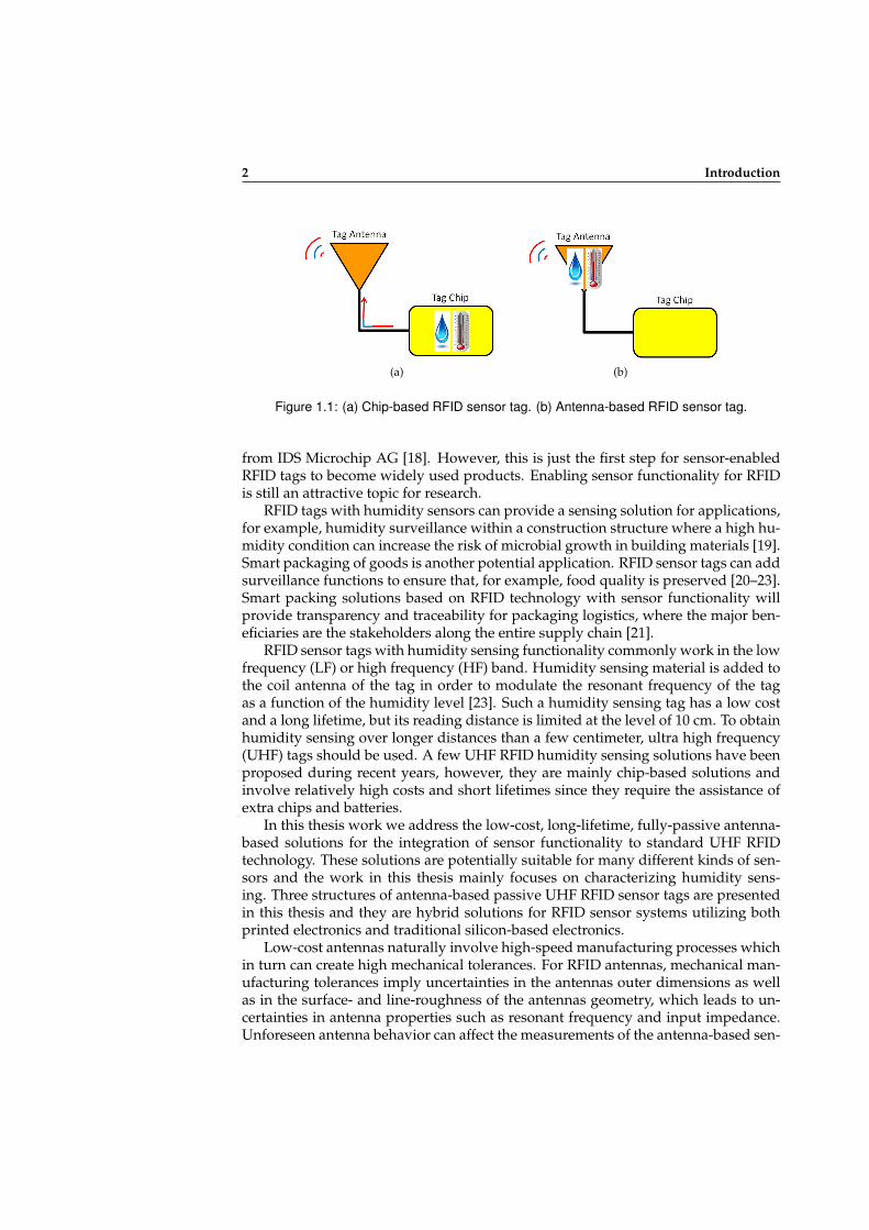
RFID, as a low cost technology with a long life time, provides great potentialfor transmitting sensor data in combination with the ordinary ID number. To adda sensing functionality into RFID tags, there are several approaches. Chip-basedsensor tag solution and antenna-based solution are two widely used approaches.As shown in Fig. 1.1, chip-based solution is to design specific RFID chips with sen-sor modules [5–8] and the antenna-based solution is to add sensor functionality toRFID tag antennas [9–16]. An RFID sensor chip has a sensor module that transformsanalog sensor information to digital numbers and communicates sensor data via anintegrated finite state machine or microcontroller. RFID sensor chips are commonlypowered by a battery or an energy harvesting module. An antenna-based RFID sen-sor tag integrates a sensor into the tag antenna in order to make the antenna’s elec-trical properties as a function of the sensor information and the RFID reader detectsthe sensor information by evaluating the tag’s communication performance. Bothapproaches have their advantages and drawbacks. For instance, the former offers agood compatibility with traditional sensors and the latter presents a longer lifetimeand lower costs. The selection of the sensor tag type depends on the applications.
The antenna-based RFID sensor tags are usually application-oriented designswhich are highly dependent on the specific applications and have not yet becomeavailable in the commercial market. While, there are several RFID sensor chipswhich have been introduced to the market, such as the HF RFID sensor chip MLX90129from Melexis Microelectronic Systems [17] and the UHF RFID sensor chip SL900A
1
2 Introduction
(a) (b)
Figure 1.1: (a) Chip-based RFID sensor tag. (b) Antenna-based RFID sensor tag.
from IDS Microchip AG [18]. However, this is just the first step for sensor-enabledRFID tags to become widely used products. Enabling sensor functionality for RFIDis still an attractive topic for research.
RFID tags with humidity sensors can provide a sensing solution for applications,for example, humidity surveillance within a construction structure where a high hu-midity condition can increase the risk of microbial growth in building materials [19].Smart packaging of goods is another potential application. RFID sensor tags can addsurveillance functions to ensure that, for example, food quality is preserved [20–23].Smart packing solutions based on RFID technology with sensor functionality willprovide transparency and traceability for packaging logistics, where the major ben-eficiaries are the stakeholders along the entire supply chain [21].
RFID sensor tags with humidity sensing functionality commonly work in the lowfrequency (LF) or high frequency (HF) band. Humidity sensing material is added tothe coil antenna of the tag in order to modulate the resonant frequency of the tagas a function of the humidity level [23]. Such a humidity sensing tag has a low costand a long lifetime, but its reading distance is limited at the level of 10 cm. To obtainhumidity sensing over longer distances than a few centimeter, ultra high frequency(UHF) tags should be used. A few UHF RFID humidity sensing solutions have beenproposed during recent years, however, they are mainly chip-based solutions andinvolve relatively high costs and short lifetimes since they require the assistance ofextra chips and batteries.
In this thesis work we address the low-cost, long-lifetime, fully-passive antenna-based solutions for the integration of sensor functionality to standard UHF RFIDtechnology. These solutions are potentially suitable for many different kinds of sen-sors and the work in this thesis mainly focuses on characterizing humidity sens-ing. Three structures of antenna-based passive UHF RFID sensor tags are presentedin this thesis and they are hybrid solutions for RFID sensor systems utilizing bothprinted electronics and traditional silicon-based electronics.
Low-cost antennas naturally involve high-speed manufacturing processes whichin turn can create high mechanical tolerances. For RFID antennas, mechanical man-ufacturing tolerances imply uncertainties in the antennas outer dimensions as wellas in the surface- and line-roughness of the antennas geometry, which leads to un-certainties in antenna properties such as resonant frequency and input impedance.Unforeseen antenna behavior can affect the measurements of the antenna-based sen-

1.1 Main contributions 3
sor tags, thus the tag antennas should be designed to be electromagnetically robustagainst edge roughness that might be introduced to the antennas during manufac-ture. The thesis’ last chapter shows an initial investigation on the effect of the edgeroughness. It shows how rough patterns along the edges of an antenna structurecan affect UHF RFID tags’ communication capabilities and the results indicate thatan antenna with a wider line width is more robust and can stand a higher degree ofedge roughness.
1.1 Main contributions
The main scientific contributions of this thesis are:
• An RFID sensor label utilizing moisture absorbing material to provide humidity sensorfunctionality to the tag antenna is presented, where the tags are based upon microstripantennas in order to suppress the influence of background materials.
The sensitivity of an antenna to the surrounding environment can be utilized toconstruct RFID sensor tags. A moisture absorbing layer placed on an RFID tagantenna can increase the humidity concentration surrounding the tag antennaand then provide wetness/humidity sensor functionality to the tag antenna.This thesis provides a solution to overcome certain limitations due to distur-bances associated with the background materials, in which microstrip anten-nas are used rather than dipole-based antennas in order to shield the influenceof the background materials. Such an antenna-based sensor tag can be used forlow-cost in-situ humidity surveillance.
• A concept of constructing RFID sensor tags is demonstrated, where a surface mount-able resistive sensor element is directly integrated into a tag antenna to construct RFIDsensor tags.
The resistive sensor can be directly embedded into the tag antenna and thesensor resistance can thus modulate the antenna performance by means of gal-vanic contact. Integration of the sensor can, for example, be achieved by seriesconnection or parallel connection with the RFID tag chip. A model-based theo-retical analysis is discussed for both two types of connections. A dipole-basedantenna is designed to characterize the performance of RFID sensor tags withsuch integration structures. The concept is demonstrated by integrating thesmall printed resistive sensors into the printed tag antennas.
• A second method of integrating a surface mountable resistive sensor element into a tagantenna is also demonstrated.
The sensor element is embedded into a loop which is positioned on top of thetag antenna and the sensor information can thus modulate the performanceof the tag antenna by means of electromagnetic (EM) coupling. The EM cou-pling mechanism is analyzed by showing how the antenna electrical properties

4 Introduction
change with sensor impedance. Two equivalent circuit models are respectivelyproposed for the EM coupled sensor tags with two different antenna structuresand the models are verified by comparison with full-wave simulation results.The proposed models can thus be a time-efficient approach to predict the per-formance of such EM coupled sensor tags through circuit-level calculations.The proposed models are suitable for analysis of EM coupled sensor tags withnot only the resistive sensors but also capacitive or inductive sensors. The keyfactors affecting the sensory performance and the methods for optimizing thesensory performance of the EM coupled RFID sensor tags are also discussed inthe thesis. The concept is experimentally verified by attaching a printed loopwith embedded resistive sensor on a commercial RFID tag.
• A printed resistive sensor element, used for demonstrating the concepts of galvaniccontact integration and electromagnetically coupled integration of a sensor into a tagantenna, is thoroughly studied and characterized in the thesis.
The sensor is an inkjet printed structure with a very small geometry. The sen-sor changes its resistance by means of an irreversible sintering process, makingit work as a write-once-read-many (WORM) memory. The WORM resistancecan be changed by either high temperature or high humidity, which impliesthat the WORM can serve as a temperature sensor or a humidity sensor. Thedrawbacks and limitations of the WORM as a sensor are discussed. The heatsintering, humidity sintering and their combinational effect are characterizedin the thesis. The humidity sensing mechanism of the printed WORM is inves-tigated through a series of experiments. The presented WORM sensor can beused to detect and record an event of excessive temperature or humidity andbe readout at a later time to provide information regarding a historical event.
• An investigation on the influence of the edge roughness on an RFID antenna is per-formed.
Edge roughness is commonly associated with low-cost high-speed antennamanufacturing processes, e.g. printing, milling, and etching process. In somecases, these manufacturing processes can cause a high degree of edge rough-ness. The edge roughness will affect the behavior of an antenna, however, thecharacteristics of edge roughness on RFID antennas have previously not re-ceived any significant attention. Unforeseen antenna behavior can affect themeasurements of the antenna-based sensor tags, thus the influence of the edgeroughness is investigated in this thesis. The investigation is performed byanalyzing the detuning of the antenna’s electrical properties caused by vari-ous degrees of edge roughness. This investigation utilizes a relatively simplestructural model to simulate the edge roughness caused by the manufactur-ing process and shows a preliminary result, where future investigations couldutilize other and more complicated structural models. However, the results ofthis investigation could advantageously constitute the basis for creating designguidelines for antennas that are robust against edge roughness.
1.2 Outline 5
• The presented three structures of the passive UHF RFID sensor tags provide both in-situ humidity sensing and historical humidity recording, at the lowest possible costlevel and being compatible with standard communication systems in logistics.
1.2 Outline
Chapter 2: Describes the methods for the acquisition of the sensor information foran antenna-based sensor tag.
Chapter 3: Describes how a layer of moisture absorbing material can provide hu-midity sensing functionality to UHF RFID tag antennas and, for such ahumidity sensor tag, how to overcome certain limitations due to distur-bances associated with background material.
Chapter 4: Describes the design and characterizations of a printed resistive humiditysensor (which is a write-once-read-many memory, WORM).
Chapter 5: Introduces the concept of UHF RFID sensor tags with sensors directlyintegrated into the antennas. The simulation results and the experimentalresults are presented.
Chapter 6: Introduces the concept of UHF RFID sensor tags with electromagneti-cally (EM) coupled sensors. Two analytical models are proposed for EMcoupled sensor tags with two different types of antenna structures. Thedesign considerations and potential optimization methods are discussed.The experimental validation is also shown in this chapter.
Chapter 7: Investigates the effect of the edge roughness on the antenna performance.
Chapter 8: Summary of publications.
Chapter 9: Thesis summary.
Chapter 10: References.

6
Chapter 2
Acquisition of the SensorInformation for anAntenna-Based Sensor Tag
An archetypal RFID system consists of an interrogator, more often known as areader, and a transponder or tag. The reader normally has one or more antennasconnected to a circuit board. The tag has an antenna and an integrated circuit (IC),often known as a silicon chip. The antennas play an important role in the commu-nication between the reader and the tag. There are many parameters that can beused to describe the electrical properties of an antenna. Input impedance, directiv-ity, gain and radiation efficiency are the most basic and most important parametersfor a tag antenna. The degree of the impedance matching between the antenna andthe load (which is the IC for the tag) determine the power transfer coefficient be-tween them. The directivity and gain describe the power magnification in differentdirections during antenna radiation. The ratio between the gain and the directivityis defined as the radiation efficiency. A radiation efficiency deviated from one indi-cates the existence of the ohmic losses in the antenna. These properties determinethe performance of the tag antenna.
Antenna-based sensory UHF RFID tags utilize the influence of the sensed physi-cal parameters on the electrical properties of a tag antenna. The sensor informationis added to the tag antenna by changing the antenna input impedance and also in-troducing ohmic losses to the antenna structure. Sometimes, the introduction of thesensor element might also cause variations of the antenna radiation pattern. The in-troduced ohmic losses cause the change in radiation efficiency of the antenna andthe eventual variation of the antenna radiation pattern is expressed by the change inantenna directivity. The product of the directivity and radiation efficiency is definedas the gain of the antenna.Therefore, the sensor information is reflected in changesin the input impedance and the gain of the antenna.
2.1 Measurable output variables
In a passive UHF RFID system, the reader transmits interrogation signals to thetags and the tags reply to the reader by means of modulating the backscattered sig-nals. The communication channel carrying information from the reader to the tagis regarded as forward link and that carrying information from the tag to the readeris regards as reverse link. In forward link, the reader transmits a power of Pt,reader
7
8 Acquisition of the Sensor Information for an Antenna-Based Sensor Tag
to its transmitting antenna (which has a gain of Greader) for power radiation andthis results in a power density of Pt,readerGreader/(4πr
2) at the position of the tagantenna, where r is the reading distance between the reader antenna and the tag an-tenna. The power received by the tag antenna (Pr,tag) is the product of the incidentpower density and the effective aperture of the tag antenna (Ae,tag), as presented inEq. 2.1. A certain percentage of the received power, determined by the power trans-fer coefficient (τ ), is transferred to the silicon chip of the tag, as described in Eq. 2.2.The power backscattered by the tag antenna (Pbs,tag) is determined by the incidentpower density and the radar scattering cross section of the tag antenna (Asc,tag), aspresented in Eq. 2.3. In a similar manner to that for the forward link, the backscat-tered power received by the reader antenna (Pr,reader) is the product of the backscat-tered power density and the effective aperture of the reader antenna (Ae,reader), aspresented in Eq. 2.4.
Pr,tag = Pt,readerGreader1
4πr2·Ae,tag (2.1)
Pr,chip = Pr,tag · τ (2.2)
Pbs,tag = Pt,readerGreader1
4πr2·Asc,tag (2.3)
Pr,reader = Pbs,tag1
4πr2·Ae,reader (2.4)
The effective aperture of the tag antenna and the reader antenna can be calcu-lated by using the standard formulas, Eq. 2.5 and Eq. 2.6, where λ is the wavelengthof electromagnetic waves at the targeted frequency and Gtag is the gain of the tagantenna. The power transfer coefficient indicates the efficiency of the antenna dueto impedance mismatch and, for the tag antenna, is calculated by Eq. 2.7 whereZC = RC + jXC and ZA = RA + jXA are respectively the chip impedance andantenna impedance. The radar scattering cross section of the tag antenna is deter-mined by the impedance and the gain of the antenna, as presented in Eq. 2.8.
Ae,tag =λ2
4πGtag (2.5)
Ae,reader =λ2
4πGreader (2.6)
τ = 1− |Γ|2 = 1−∣∣∣∣ ZC − Z∗
A
ZC + ZA
∣∣∣∣2 =4RCRA
|ZC + ZA |2(2.7)
Asc,tag =λ2
4πG2
tag
4R2A
|ZC + ZA|2=
λ2
4πG2
tag
RA
RCτ (2.8)

2.1 Measurable output variables 9
To power up the chip, Pr,chip should not be less than the chip sensitivity PC whichis the minimum power required to activate the tag IC.
Pr,chip ≥ PC (2.9)
Since RFID systems are commonly forward link limited [24] and the chip sensi-tivity PC is constant, the maximum reading distance of the RFID tag and the mini-mum reader transmit power required for IC power-up can be derived from forwardpower transmission equations (Eq. 2.1, 2.2 and 2.9). With successful forward powertransmission, the backscattered power is received by the reader and the power levelrelates to the radar scattering cross section of the tag antenna.
Based on the analysis above, we can conclude that
(a) the maximum reading distance (rmax) is proportional to the square root of thepower transfer coefficient and the gain of tag antenna when the transmit powerfrom the reader is a constant, as presented in Eq. 2.10;
rmax ∝√
τ ·Gtag (2.10)
(b) the required minimum transmit power (Pt,readermin ) is inversely proportionalto the power transfer coefficient and the gain of tag antenna when the readingdistance is fixed as a constant, as presented in Eq. 2.11;
Pt,readermin ∝ 1
τ ·Gtag(2.11)
(c) the backscattered power received by the reader (Pr,reader) is proportional tothe radar scattering cross-section (Asc,tag) of the tag antenna when the readertransmit power and the reading distance are constants, as presented in Eq. 2.12.
Pr,reader ∝ Asc,tag (2.12)
As mentioned at the beginning of this chapter, the sensor information is reflectedin changes in the input impedance and the gain of the antenna. At the same time,changes in the impedance and the gain of the antenna can be obtained by measuringthe change in one of the three variables, rmax, Pt,readermin
and Pr,reader. The changesin these three variables can thus be related to the sensing information.
It should, however, be mentioned that Eq. 2.1-2.4 are only really accurate for free-space propagation and anechoic environments. A more exact model must accountfor additional factors such as multipath and small- and large-scale fading [25, 26].Therefore, the above equations present a simplistic approximation to an ideal situa-tion and are thus optimistic.
10 Acquisition of the Sensor Information for an Antenna-Based Sensor Tag
2.2 Measurement setup
To facilitate the acquisition of the sensor data, setting the reader transmit poweras a constant is easily accomplished by setting up the parameters for the reader.However, for long term measurements of a sensor tag, maintaining the reading dis-tance at a fixed constant value is not a good option. Thus, to remove the requirementof fixed reading distances, a twin tag setup is necessary. The twin tag setup wasfirstly presented in [10]. In such a twin tag setup, one of the tags is a sensor tag andthe other is a normal tag, which is used as a reference. The reference tag has thesame kind of antenna and chip as those in the sensor tag, but without the sensorelement. Two identical RFID tags are applied within the same sensor label and theyare always interrogated at the same reading distance, thus allowing for a differentialpower readout.
According to Eq. 2.11, the ratio between the required minimum transmit powerfor a sensor tag and for a normal tag is determined by the inverse ratio of the powertransfer coefficient and the gain of the tag antennas when the two tags are interro-gated at the same reading distance. That is, the relative required minimum transmitpower for a sensor tag compared to a normal tag is determined by Eq. 2.13 and Equa-tion 2.14 produces results in decibel units. The relative required minimum transmitpower in decibel is also referred to as the transmitted power difference. Similarly,according to Eq. 2.12, the relative value of the reader received power for a sensor tagcompared to a normal tag can be expressed by the ratio between the radar scatteringcross section for a sensor tag and for a normal tag when the two tags are interrogatedat the same reading distance. Since the radar scattering cross section is also a func-tion of the antenna impedance and gain, the relative reader received power can befinally expressed through the ratios of the antenna impedance and gain, as presentedin Eq. 2.15 and Eq. 2.16. The detuning of the antenna electrical properties caused bythe introduction of a sensor into the tag antenna can thus be evaluated in terms ofthe relative required minimum transmit power or the relative reader received powerwithout the restriction of fixed reading distance.
P relativet,readermin
=P sensort,readermin
Pnormalt,readermin
=
(τ ·Gtag
τ0 ·Gtag0
)−1
(2.13)
P relativet,readermin
[dB] = P sensort,readermin
[dBm]− Pnormalt,readermin
[dBm] = −10 log10
(τ ·Gtag
τ0 ·Gtag0
)(2.14)
P relativer,reader =
P sensorr,reader
Pnormalr,reader
=Asc
Asc0=
G2tag ·RA · τ
G2tag0 ·RA0 · τ0
(2.15)
P relativer,reader[dB] = P sensor
r,reader[dBm]−Pnormalr,reader[dBm] = 10 log10
(G2
tag ·RA · τG2
tag0 ·RA0 · τ0
)(2.16)
2.2 Measurement setup 11
In Eq. 2.13-2.16, the variables with subscript “0” represent the parameters of thenormal tag antenna and the corresponding variables without subscript “0” repre-sent the parameters of the sensor tag antenna. This is always true throughout theremainder of this thesis.
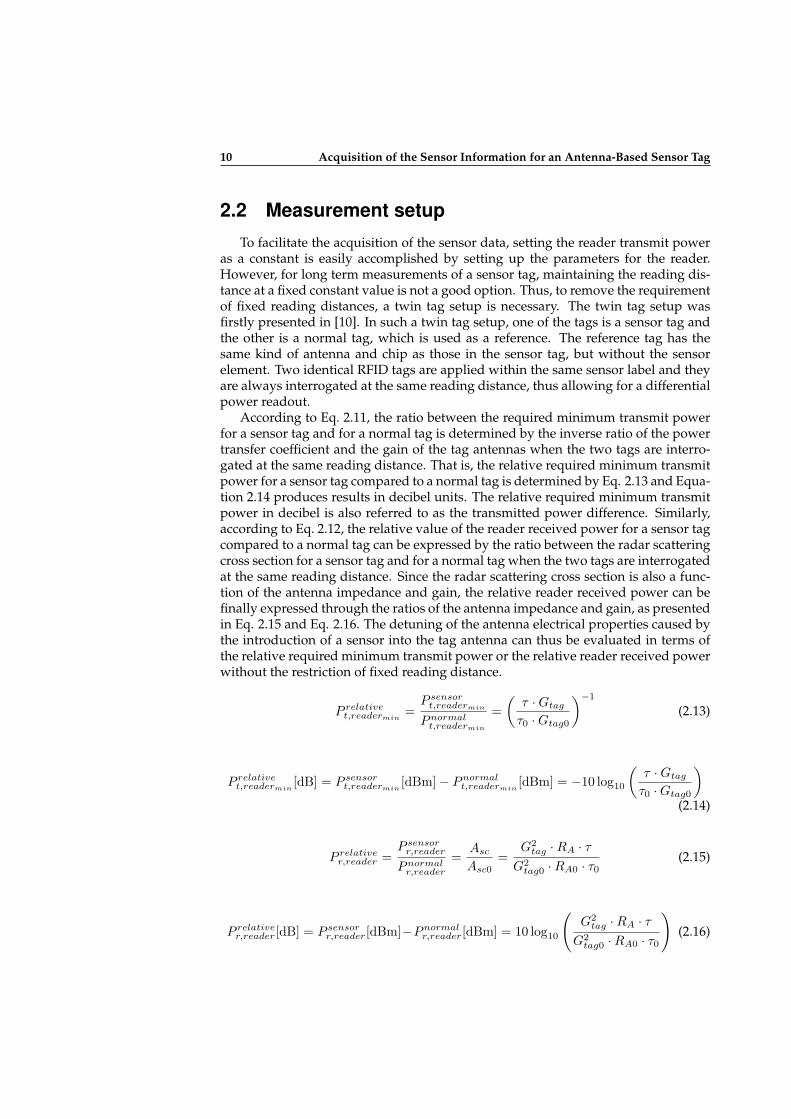
Both the differential output power transmitted by the reader and the differentialbackscattered power received by the reader can be obtained using a twin-tag setupand they are related to the sensing information. The work in this thesis was carriedout mainly by measuring the differential output power. Fig. 2.1 illustrates this twintag method for the case used in this thesis work. The sensor tag and the referencetag are placed in a label and an RFID reader antenna is placed in front of the tags.The distance between the two tags is relatively small in comparison to the distancebetween the RFID reader and the sensor label. The distance from the reader to eachtag can thus be treated as the same value. A GUI PC software was developed tocontrol the reader to sweep the output power and record the minimum power levelsrequired to read each tag within a label. The power sweep can be set to automaticallyrun several times in order to create an average value for each experiment since avariation of ±0.5 dB for output power is relatively common.
Figure 2.1: Illustration of the twin tag concept.

12
Chapter 3
UHF RFID Sensor Tags WithCovering of Sensing Material
It is well known that the performance of low cost tags, constructed with simpleone-layer antennas, is very sensitive to the surrounding environment and especiallyto nearby metallic surfaces and water [27–29]. The water content nearby an RFIDantenna will directly cause ohmic losses in the antennas near-field and also changeits resonance frequency. It has previously been characterized as to how this propertycan be used to measure the wetness in soil and snow by connecting a transmissionline to a buried monopole antenna [30].
If the RFID tag is covered by or totally embedded in a moisture absorbing ma-terial, the tag performance will relate to the water concentration in the moisture ab-sorbing material. Considering the previously mentioned differential readout methodusing a twin-tag setup, one of the RFID tags is covered by or totally embedded in amoisture absorbing material while the other tag remains naked. In a humid envi-ronment, the humidity concentration will thus be higher in the moisture absorbingmaterial than in the vicinity of an naked tag [31]. The performance of the embeddedtag will be worse than that of the naked tag. The difference in performance of thetwo tags will thus be related to the level of relative humidity.
[10] demonstrates a humidity RFID sensor solution with an antenna covered bymoisture absorbing paper. Paper material is known to withdraw water and in a hu-mid environment, the water concentration in a paper material is a function of therelative humidity in the surrounding air [32]. As water will increase both the realand imaginary parts of the papers dielectric constant, the tag antenna will operatewith lower efficiency due to the changes in input impedance and ohmic losses. Thatis, the humidity will eventually cause a degradation of the tag performance. AnRFID reader positioned in front of the twin-tag label must thus emit a stronger in-terrogating signal in order to power up the embedded tag than that required by thenaked tag. By comparing the minimum power levels required to power up each tag,it is therefore possible to determine the humidity level at the tag’s location. In thefield the procedure requires a lookup table where moisture levels previously havebeen characterized versus differences in power up levels.
As mentioned, the basic concept regarding the RFID sensor tags utilizing mois-ture absorbing material has been characterized previously by embedding ordinarycommercially available RFID tags in a paper material. Readout problems can how-ever occur when these one-layer antennas are placed on a background material thatalso contains a moisture absorbing material, such as wood, or containing nails orscrews or something else that might disturb the measurement.
13
14 UHF RFID Sensor Tags With Covering of Sensing Material
Therefore, in this chapter, we present how UHF RFID tags with microstrip anten-nas could be used for measuring levels of relative humidity at hidden locations andthus shield the background materials. The microstrip antennas’ low influence frombackground materials in combination with making them more narrow-banded thancommercial tags ensures that the differential readout becomes more reliable.
3.1 Experimental results
It is well known that the performance of low cost tags,
constructed with simple one-layer antennas, is very sensitive
to the surrounding environment and especially to nearby
]. Water content nearby an
RFID antenna will directly cause ohmic losses in the
ange its resonance frequency.
ized how this property can be
used to measure humidity at a hidden location with aid of
pairs of ordinary passive RFID tags by covering or totally
embedding one of the two tags with a moisture absorbing
material while the other tag is left untouched [4]. Paper
material is known to withdraw water and in a humid
environment the humidity concentration will thus be higher
in the moisture absorbing material than in the vicinity of an
As water will increase both the real and imaginary parts of
the paper’s dielectric constant, the tag antenna will operate
with lower efficiency due to ohmic losses and change in
input impedance. If the tags are passive, an RFID reader
positioned at the same distance from both tags in the label
characterized versus differences in power up levels.
Fig. 2. Drawing of the pair of microstrip antennas where one
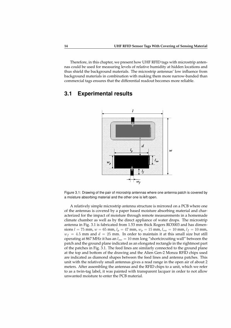
antenna patch is covered by a moisture absorbing material. Figure 3.1: Drawing of the pair of microstrip antennas where one antenna patch is covered bya moisture absorbing material and the other one is left open.
A relatively simple microstrip antenna structure is mirrored on a PCB where oneof the antennas is covered by a paper based moisture absorbing material and char-acterized for the impact of moisture through remote measurements in a homemadeclimate chamber as well as by the direct appliance of water drops. The microstripantenna in Fig. 3.1 is fabricated from 1.53 mm thick Rogers RO3003 and has dimen-sions l = 75 mm, w = 65 mm, lp = 47 mm, wp = 15 mm, lsw = 10 mm, lf = 10 mm,wf = 4.5 mm and d = 25 mm. In order to maintain it at this small size but stilloperating at 867 MHz it has an lsw = 10 mm long ”shortcircuiting wall” between thepatch and the ground plane indicated as an elongated rectangle in the rightmost partof the patches in Fig. 3.1. The feed lines are similarly connected to the ground planeat the top and bottom of the drawing and the Alien Gen-2 Monza RFID chips usedare indicated as diamond shapes between the feed lines and antenna patches. Thisunit with the relatively small antennas gives a read range in the open air of about 2meters. After assembling the antennas and the RFID chips to a unit, which we referto as a twin-tag label, it was painted with transparent lacquer in order to not allowunwanted moisture to enter the PCB material.
3.1 Experimental results 15
The upper antenna in Fig. 3.1 was covered with, respectively, one and three500 µm thick blotting papers known to have a high ability to withdraw moisture.The reason for attempting two different total thicknesses is to evaluate how much athicker moisture absorbing layer affects the antenna degradation. To further evalu-ate how to increase the impact of moisture, some absorbing papers were also dopedwith NaCl in order to increase the ohmic losses when moisture enters the paper.
The experimental tags were placed in a 1 x 1 x 0.1 meter large climate chamberand a SAMSys RFID reader was placed outside with its reader antenna 0.80 metersfrom the tags inside the chamber. For each experiment the output power of theSAMSys reader was swept from 12.0 dBm to 28.0 dBm with a 5 dBi reader antenna.The minimum output powers required to read the open tag and the embedded tagwere recorded and compared in order to obtain the differential power value.
3.1.1 Power-up differences due to water drops
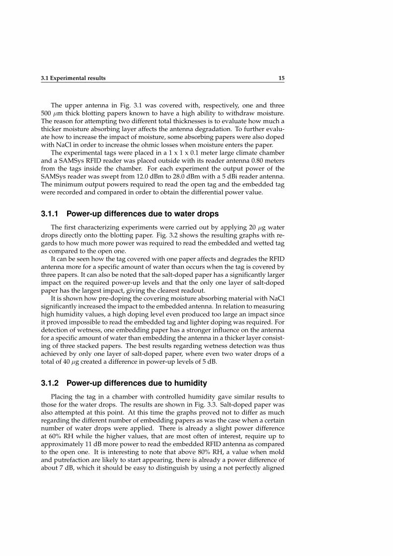
The first characterizing experiments were carried out by applying 20 µg waterdrops directly onto the blotting paper. Fig. 3.2 shows the resulting graphs with re-gards to how much more power was required to read the embedded and wetted tagas compared to the open one.
It can be seen how the tag covered with one paper affects and degrades the RFIDantenna more for a specific amount of water than occurs when the tag is covered bythree papers. It can also be noted that the salt-doped paper has a significantly largerimpact on the required power-up levels and that the only one layer of salt-dopedpaper has the largest impact, giving the clearest readout.
It is shown how pre-doping the covering moisture absorbing material with NaClsignificantly increased the impact to the embedded antenna. In relation to measuringhigh humidity values, a high doping level even produced too large an impact sinceit proved impossible to read the embedded tag and lighter doping was required. Fordetection of wetness, one embedding paper has a stronger influence on the antennafor a specific amount of water than embedding the antenna in a thicker layer consist-ing of three stacked papers. The best results regarding wetness detection was thusachieved by only one layer of salt-doped paper, where even two water drops of atotal of 40 µg created a difference in power-up levels of 5 dB.
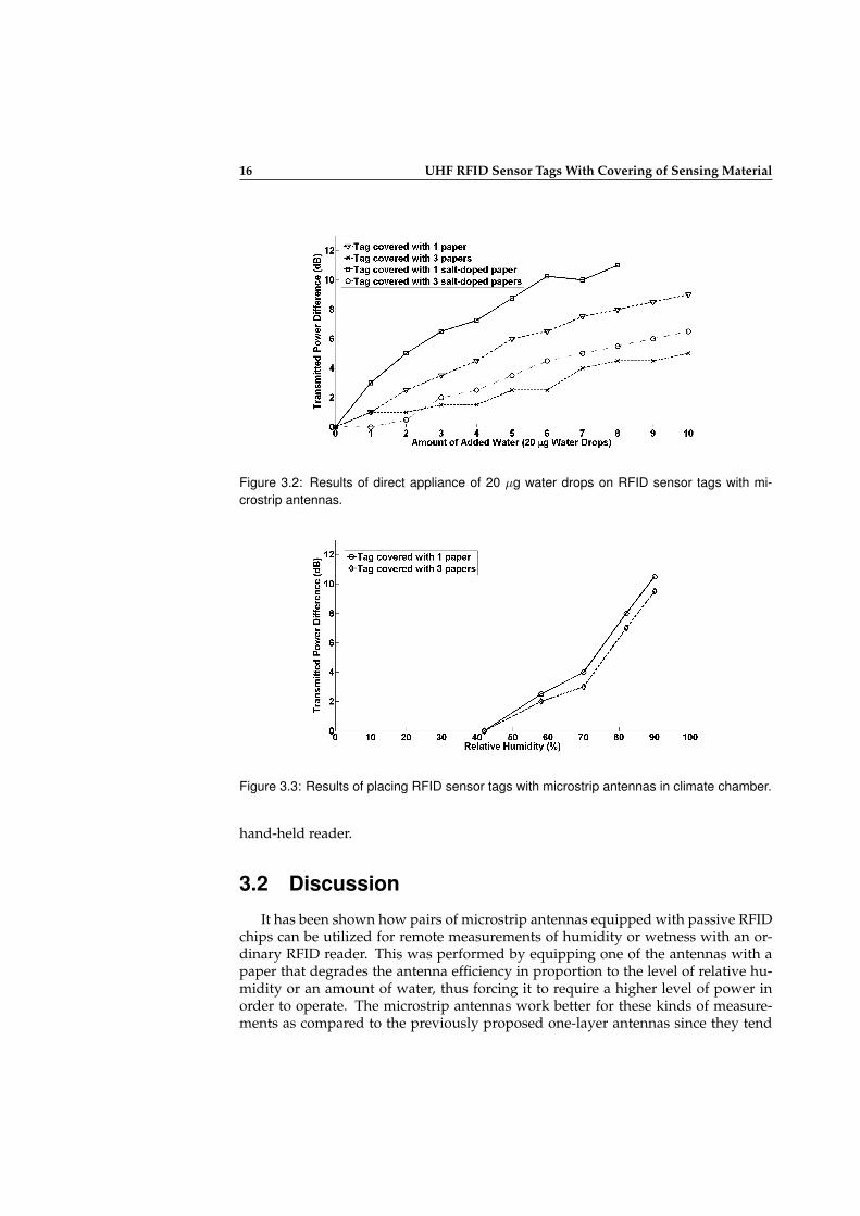
3.1.2 Power-up differences due to humidity
Placing the tag in a chamber with controlled humidity gave similar results tothose for the water drops. The results are shown in Fig. 3.3. Salt-doped paper wasalso attempted at this point. At this time the graphs proved not to differ as muchregarding the different number of embedding papers as was the case when a certainnumber of water drops were applied. There is already a slight power differenceat 60% RH while the higher values, that are most often of interest, require up toapproximately 11 dB more power to read the embedded RFID antenna as comparedto the open one. It is interesting to note that above 80% RH, a value when moldand putrefaction are likely to start appearing, there is already a power difference ofabout 7 dB, which it should be easy to distinguish by using a not perfectly aligned
16 UHF RFID Sensor Tags With Covering of Sensing Material
Figure 3.2: Results of direct appliance of 20 µg water drops on RFID sensor tags with mi-crostrip antennas.
that the combination of only one paper and having that one
doped with salt has the largest impact, giving the clearest
Placing the tag in a chamber with controlled humidity gave
similar results as for the water drops as is shown in Fig. 4.
Salt-doped paper was tried also here but the heavily doped
had too large impact on the
antenna as the embedded tag could not be read even at 80%
RH. A less doped paper was therefore used with the results
Limitations of the proposed measurement concept includes
Fig. 4. Results from experiments in climate chamber. There is a
slight power difference already at 60% RH while the higher Figure 3.3: Results of placing RFID sensor tags with microstrip antennas in climate chamber.
hand-held reader.
3.2 Discussion
It has been shown how pairs of microstrip antennas equipped with passive RFIDchips can be utilized for remote measurements of humidity or wetness with an or-dinary RFID reader. This was performed by equipping one of the antennas with apaper that degrades the antenna efficiency in proportion to the level of relative hu-midity or an amount of water, thus forcing it to require a higher level of power inorder to operate. The microstrip antennas work better for these kinds of measure-ments as compared to the previously proposed one-layer antennas since they tend

3.2 Discussion 17
to be less sensitive to it background material. Evaluated microstrip antennas werealso designed to have a narrower bandwidth than the common commercial one-layer RFID antennas, making them more sensitive to dielectric changes in a materialembedding the antenna.
It was also shown how pre-doping the covering moisture absorbing material withNaCl significantly increased the impact to the embedded antenna. In relation to mea-suring high humidity values, a high doping level even produced too large impactsince the embedded tag was no longer readable and lighter doping was required.For the detection of wetness, it was further experienced that one embedding paperhad a stronger influence on the antenna for a specific amount of water than embed-ding the antenna in a thicker layer consisting of three stacked papers. The best resultsfor wetness detection were thus achieved by using only one layer of salt-doped pa-per, where even just two water drops totaling 40 µg created a difference in power-uplevels of 5 dB.
The method of covering the tag with a layer of special material could also, poten-tially, be utilized to measure other physical quantities as long as there is a materialto be placed over the tag antenna that changes its electrical properties in proportionto the physical quantity of interest.

18
Chapter 4
Printed Sensor (WORM)In the previous chapter, the moisture absorbing material provided humidity sens-
ing functionality to RFID tag antennas that in turn provided information regardingthe current humidity status through an RFID readout method. This chapter presentsan ultra-low cost humidity sensor element with memory functionality. It is a 1-bitwrite-once-read-many (WORM) memory printed using conductive ink based uponnanometer-sized silver particles. The printed WORM is suitable for direct integra-tion into a printed RFID antenna or other printed circuits. As a sensor componentthe WORM exhibits two states, “On” and “Off”, corresponding to “WORM bit = 1”and “WORM bit = 0”. The printed WORM memory is defined by means of its resis-tance and in which a logical zero equals a high resistance and a logical one equals alower resistance. The setting for this bit is accomplished by means of sintering.
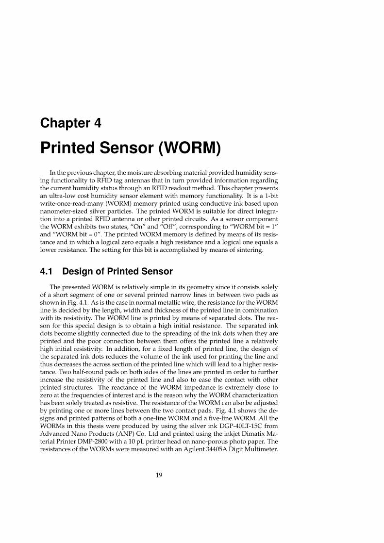
4.1 Design of Printed Sensor
The presented WORM is relatively simple in its geometry since it consists solelyof a short segment of one or several printed narrow lines in between two pads asshown in Fig. 4.1. As is the case in normal metallic wire, the resistance for the WORMline is decided by the length, width and thickness of the printed line in combinationwith its resistivity. The WORM line is printed by means of separated dots. The rea-son for this special design is to obtain a high initial resistance. The separated inkdots become slightly connected due to the spreading of the ink dots when they areprinted and the poor connection between them offers the printed line a relativelyhigh initial resistivity. In addition, for a fixed length of printed line, the design ofthe separated ink dots reduces the volume of the ink used for printing the line andthus decreases the across section of the printed line which will lead to a higher resis-tance. Two half-round pads on both sides of the lines are printed in order to furtherincrease the resistivity of the printed line and also to ease the contact with otherprinted structures. The reactance of the WORM impedance is extremely close tozero at the frequencies of interest and is the reason why the WORM characterizationhas been solely treated as resistive. The resistance of the WORM can also be adjustedby printing one or more lines between the two contact pads. Fig. 4.1 shows the de-signs and printed patterns of both a one-line WORM and a five-line WORM. All theWORMs in this thesis were produced by using the silver ink DGP-40LT-15C fromAdvanced Nano Products (ANP) Co. Ltd and printed using the inkjet Dimatix Ma-terial Printer DMP-2800 with a 10 pL printer head on nano-porous photo paper. Theresistances of the WORMs were measured with an Agilent 34405A Digit Multimeter.
19
20 Printed Sensor (WORM)
(a) (b)
(c) (d)
Figure 4.1: The printed WORM structure with (a)-(b) one sensor line and (c)-(d) five parallelsensor lines.
4.2 Temperature Sintering
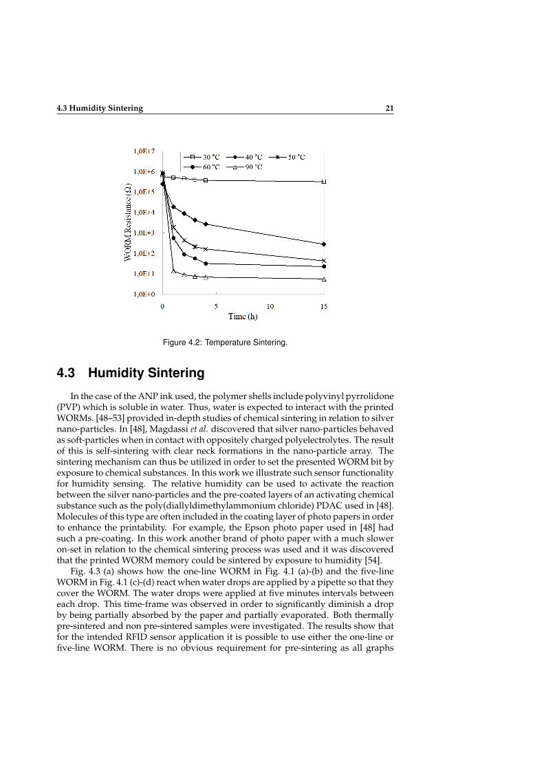
In nano-particle inks, the metal particles are stabilized by one or more disper-sants or by capping agents. The capping agents create an electrostatic and/or stericbarrier which prevents the aggregation of the particles. In a printed trace, the nanoparticles are embedded in an insulating polymer matrix which impedes electricalconductance [33]. Sintering is required in most cases to reach high conductance. Sin-tering is a process used in order to enhance junctions among particles and to reduceresistivity by means of thermal heating in an oven or by applying a current flow,intense pulsed light, microwave or a laser [34–47]. High temperatures can causethis reduction of resistivity by melting the encapsulating polymers of the silver nanoparticles and also by evaporating the solvent and binders in the ink, which, in turn,cause a neck formation and particle growth. Fig. 4.2 shows the effect of thermalsintering at different temperatures, taking the five-line WORM as an example. TheWORM could be sintered by a temperature higher than 30 C. The sintering velocityis proportional to the temperature.
4.3 Humidity Sintering 21
Figure 4.2: Temperature Sintering.
4.3 Humidity Sintering
In the case of the ANP ink used, the polymer shells include polyvinyl pyrrolidone(PVP) which is soluble in water. Thus, water is expected to interact with the printedWORMs. [48–53] provided in-depth studies of chemical sintering in relation to silvernano-particles. In [48], Magdassi et al. discovered that silver nano-particles behavedas soft-particles when in contact with oppositely charged polyelectrolytes. The resultof this is self-sintering with clear neck formations in the nano-particle array. Thesintering mechanism can thus be utilized in order to set the presented WORM bit byexposure to chemical substances. In this work we illustrate such sensor functionalityfor humidity sensing. The relative humidity can be used to activate the reactionbetween the silver nano-particles and the pre-coated layers of an activating chemicalsubstance such as the poly(diallyldimethylammonium chloride) PDAC used in [48].Molecules of this type are often included in the coating layer of photo papers in orderto enhance the printability. For example, the Epson photo paper used in [48] hadsuch a pre-coating. In this work another brand of photo paper with a much sloweron-set in relation to the chemical sintering process was used and it was discoveredthat the printed WORM memory could be sintered by exposure to humidity [54].
Fig. 4.3 (a) shows how the one-line WORM in Fig. 4.1 (a)-(b) and the five-lineWORM in Fig. 4.1 (c)-(d) react when water drops are applied by a pipette so that theycover the WORM. The water drops were applied at five minutes intervals betweeneach drop. This time-frame was observed in order to significantly diminish a dropby being partially absorbed by the paper and partially evaporated. Both thermallypre-sintered and non pre-sintered samples were investigated. The results show thatfor the intended RFID sensor application it is possible to use either the one-line orfive-line WORM. There is no obvious requirement for pre-sintering as all graphs
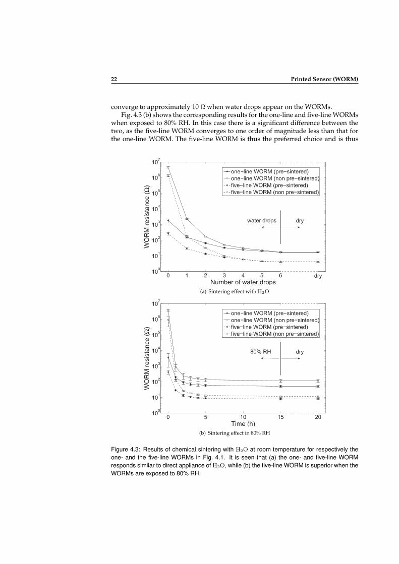
22 Printed Sensor (WORM)
converge to approximately 10 Ω when water drops appear on the WORMs.Fig. 4.3 (b) shows the corresponding results for the one-line and five-line WORMs
when exposed to 80% RH. In this case there is a significant difference between thetwo, as the five-line WORM converges to one order of magnitude less than that forthe one-line WORM. The five-line WORM is thus the preferred choice and is thus
0 1 2 3 4 5 6 810
0
101
102
103
104
105
106
107
Number of water drops
WO
RM
resis
tance (
Ω)
one−line WORM (pre−sintered)
one−line WORM (non pre−sintered)
five−line WORM (pre−sintered)
five−line WORM (non pre−sintered)
dry
water drops dry
_ _ _ _ _ _ _ _ _ _ _ _ _
_ _ _ _ _ _ _ _ _ _ _ _ _
(a) Sintering effect with H2O
0 5 10 15 2010
0
101
102
103
104
105
106
107
Time (h)
WO
RM
resis
tance (
Ω)
one−line WORM (pre−sintered)
one−line WORM (non pre−sintered)
five−line WORM (pre−sintered)
five−line WORM (non pre−sintered)
dry80% RH
_ _ _ _ _ _ _ _ _ _ _ _ _
_ _ _ _ _ _ _ _ _ _ _ _ _
(b) Sintering effect in 80% RH
Figure 4.3: Results of chemical sintering with H2O at room temperature for respectively theone- and the five-line WORMs in Fig. 4.1. It is seen that (a) the one- and five-line WORMresponds similar to direct appliance of H2O, while (b) the five-line WORM is superior when theWORMs are exposed to 80% RH.
4.4 Combination Effect of Temperature and Humidity 23
used in the subsequent experiments. Fig. 4.3 also shows that the sintered WORMresistance remains at its lowest achieved value if the WORM is placed back to adry condition. That is, the humidity sintering effect is irreversible. The results inFig. 4.3 were obtained by averaging the resistance of ten samples. The small standarddeviations indicate that the humidity sintering of the WORM has good repeatability.
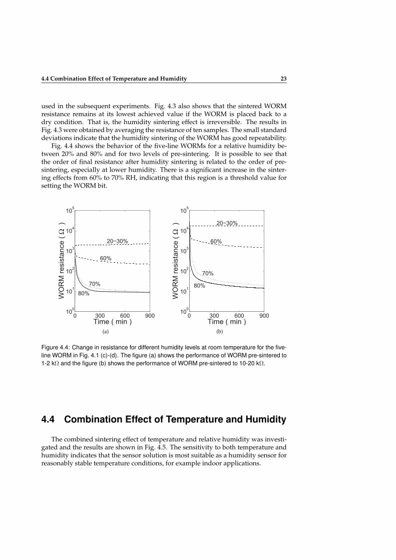
Fig. 4.4 shows the behavior of the five-line WORMs for a relative humidity be-tween 20% and 80% and for two levels of pre-sintering. It is possible to see thatthe order of final resistance after humidity sintering is related to the order of pre-sintering, especially at lower humidity. There is a significant increase in the sinter-ing effects from 60% to 70% RH, indicating that this region is a threshold value forsetting the WORM bit.
0 300 600 90010
0
101
102
103
104
105
Time ( min )
WO
RM
resis
tance (
Ω
)
WO
RM
resis
tance (
)
20 30%
60%
70%
80%
(a)
900)
0 300 600 90010
0
101
102
103
104
105
Time ( min )
WO
RM
resis
tance (
Ω
) 20 30%
60%
80%
70%
(b)
Figure 4.4: Change in resistance for different humidity levels at room temperature for the five-line WORM in Fig. 4.1 (c)-(d). The figure (a) shows the performance of WORM pre-sintered to1-2 kΩ and the figure (b) shows the performance of WORM pre-sintered to 10-20 kΩ.
4.4 Combination Effect of Temperature and Humidity
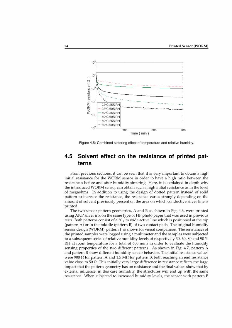
The combined sintering effect of temperature and relative humidity was investi-gated and the results are shown in Fig. 4.5. The sensitivity to both temperature andhumidity indicates that the sensor solution is most suitable as a humidity sensor forreasonably stable temperature conditions, for example indoor applications.
24 Printed Sensor (WORM)
300 600 90010
0
101
102
103
104
105
Time ( min )
WO
RM
resis
tance (
Ω
)
22°C 25%RH
22°C 60%RH
40°C 25%RH
40°C 60%RH
50°C 25%RH
50°C 60%RH
Figure 4.5: Combined sintering effect of temperature and relative humidity.
4.5 Solvent effect on the resistance of printed pat-terns
From previous sections, it can be seen that it is very important to obtain a highinitial resistance for the WORM sensor in order to have a high ratio between theresistances before and after humidity sintering. Here, it is explained in depth whythe introduced WORM sensor can obtain such a high initial resistance as in the levelof megaohms. In addition to using the design of dotted pattern instead of solidpattern to increase the resistance, the resistance varies strongly depending on theamount of solvent previously present on the area on which conductive silver line isprinted.
The two sensor pattern geometries, A and B as shown in Fig. 4.6, were printedusing ANP silver ink on the same type of HP photo paper that was used in previoustests. Both patterns consist of a 30 µm wide active line which is positioned at the top(pattern A) or in the middle (pattern B) of two contact pads. The original humiditysensor design (WORM), pattern 1, is shown for visual comparison. The resistances ofthe printed samples were logged using a multimeter and the samples were subjectedto a subsequent series of relative humidity levels of respectively 30, 60, 80 and 90 %RH at room temperature for a total of 600 mins in order to evaluate the humiditysensing properties of the two different patterns. As shown in Fig. 4.7, pattern Aand pattern B show different humidity sensor behavior. The initial resistance valueswere 900 Ω for pattern A and 1.5 MΩ for pattern B, both reaching an end resistancevalue close to 50 Ω. This initially very large difference in resistance reflects the largeimpact that the pattern geometry has on resistance and the final values show that byexternal influence, in this case humidity, the structures will end up with the sameresistance. When subjected to increased humidity levels, the sensor with pattern B
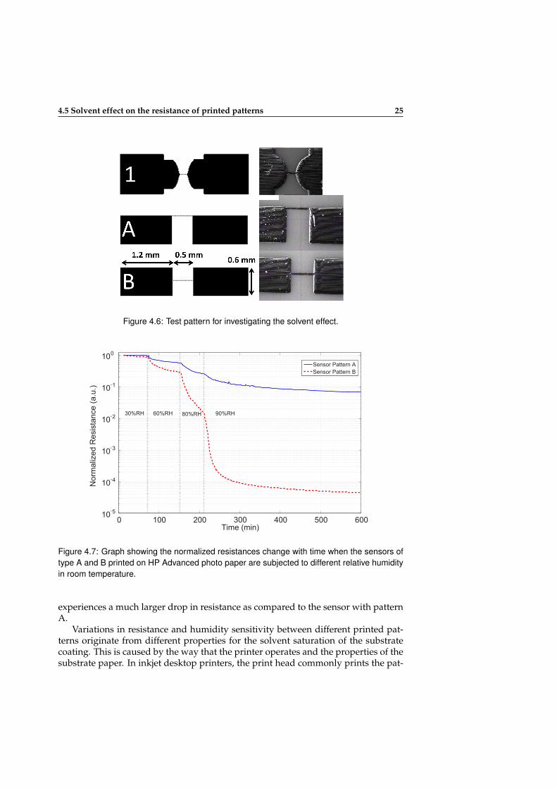
4.5 Solvent effect on the resistance of printed patterns 25
Figure 4.6: Test pattern for investigating the solvent effect.
0 100 200 400 500 60010
−5
10−4
10−3
10−2
10−1
100
300
Time (min)
Norm
aliz
ed R
esis
tance (
a.u
.)
Sensor Pattern A
Sensor Pattern B
90%RH30%RH 80%RH60%RH
Figure 4.7: Graph showing the normalized resistances change with time when the sensors oftype A and B printed on HP Advanced photo paper are subjected to different relative humidityin room temperature.
experiences a much larger drop in resistance as compared to the sensor with patternA.
Variations in resistance and humidity sensitivity between different printed pat-terns originate from different properties for the solvent saturation of the substratecoating. This is caused by the way that the printer operates and the properties of thesubstrate paper. In inkjet desktop printers, the print head commonly prints the pat-
26 Printed Sensor (WORM)
terns with horizontal lines by passing from left to right, starting at the top line andending at the bottom. The photo paper substrates commonly have a coating layer ofseveral tens of µm that are specifically applied to quickly absorb and spread the inksolvents. In pattern A, the active sensor line is printed first, and no extra solvent ispresent in the paper substrate at the time of printing. In pattern B and pattern 1, halfof the contact pads that connect the active line are printed first and the active sensorline will be printed on a part of the substrate that has already received some solventspreading out from the contact pads. Therefore, from Fig. 4.7, it can be concludedthat the humidity sensitivity of the printed sensor line depends on the amount ofsolvent that is present on the printing area at the time of printing the active sensorline.
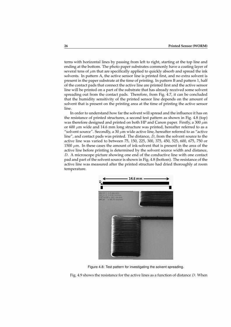
In order to understand how far the solvent will spread and the influence it has onthe resistance of printed structures, a second test pattern as shown in Fig. 4.8 (top)was therefore designed and printed on both HP and Canon paper. Firstly, a 300 µmor 600 µm wide and 14.6 mm long structure was printed, hereafter referred to as a“solvent source”. Secondly, a 30 µm wide active line, hereafter referred to as “activeline”, and contact pads was printed. The distance, D, from the solvent source to theactive line was varied to between 75, 150, 225, 300, 375, 450, 525, 600, 675, 750 or1500 µm. In these cases the amount of ink-solvent that is present in the area of theactive line before printing is determined by the solvent source width and distance,D. A microscope picture showing one end of the conductive line with one contactpad and part of the solvent source is shown in Fig. 4.8 (bottom). The resistance of theactive line was measured after the printed structure had dried thoroughly at roomtemperature.
Figure 4.8: Test pattern for investigating the solvent spreading.
Fig. 4.9 shows the resistance for the active lines as a function of distance D. When
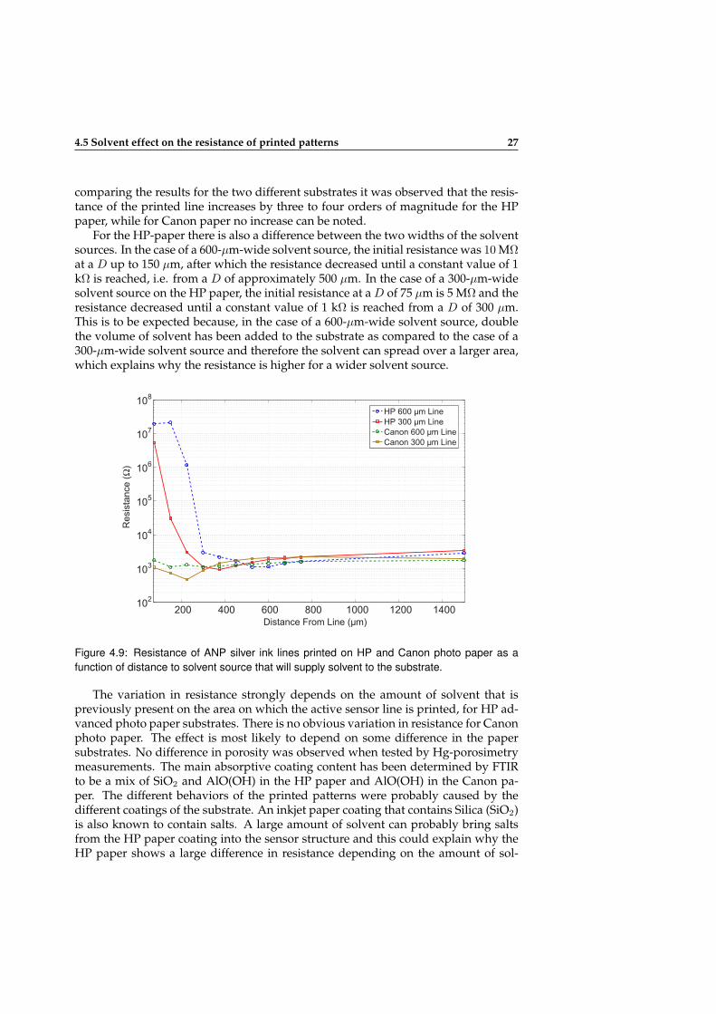
4.5 Solvent effect on the resistance of printed patterns 27
comparing the results for the two different substrates it was observed that the resis-tance of the printed line increases by three to four orders of magnitude for the HPpaper, while for Canon paper no increase can be noted.
For the HP-paper there is also a difference between the two widths of the solventsources. In the case of a 600-µm-wide solvent source, the initial resistance was 10 MΩat a D up to 150 µm, after which the resistance decreased until a constant value of 1kΩ is reached, i.e. from a D of approximately 500 µm. In the case of a 300-µm-widesolvent source on the HP paper, the initial resistance at a D of 75 µm is 5 MΩ and theresistance decreased until a constant value of 1 kΩ is reached from a D of 300 µm.This is to be expected because, in the case of a 600-µm-wide solvent source, doublethe volume of solvent has been added to the substrate as compared to the case of a300-µm-wide solvent source and therefore the solvent can spread over a larger area,which explains why the resistance is higher for a wider solvent source.
200 400 600 800 1000 1200 140010
2
103
104
105
106
107
108
Distance From Line (µm)
Resis
tance (
Ω)
HP 600 µm Line
HP 300 µm Line
Canon 600 µm Line
Canon 300 µm Line
Figure 4.9: Resistance of ANP silver ink lines printed on HP and Canon photo paper as afunction of distance to solvent source that will supply solvent to the substrate.
The variation in resistance strongly depends on the amount of solvent that ispreviously present on the area on which the active sensor line is printed, for HP ad-vanced photo paper substrates. There is no obvious variation in resistance for Canonphoto paper. The effect is most likely to depend on some difference in the papersubstrates. No difference in porosity was observed when tested by Hg-porosimetrymeasurements. The main absorptive coating content has been determined by FTIRto be a mix of SiO2 and AlO(OH) in the HP paper and AlO(OH) in the Canon pa-per. The different behaviors of the printed patterns were probably caused by thedifferent coatings of the substrate. An inkjet paper coating that contains Silica (SiO2)is also known to contain salts. A large amount of solvent can probably bring saltsfrom the HP paper coating into the sensor structure and this could explain why theHP paper shows a large difference in resistance depending on the amount of sol-
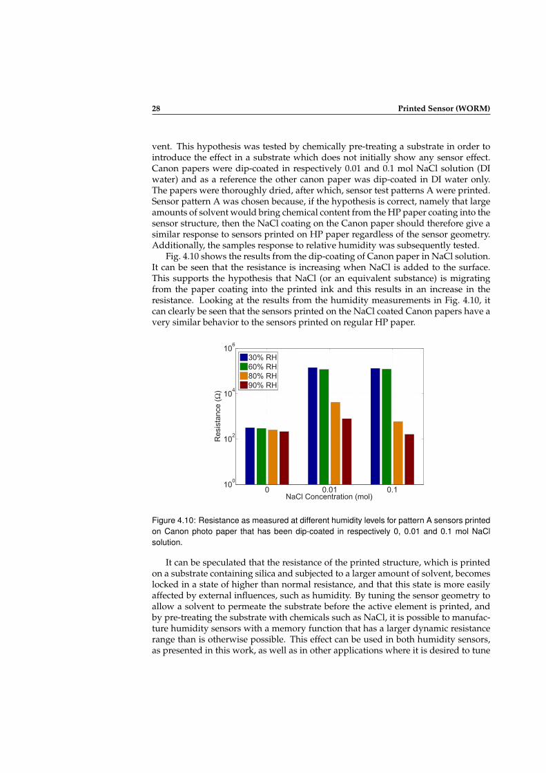
28 Printed Sensor (WORM)
vent. This hypothesis was tested by chemically pre-treating a substrate in order tointroduce the effect in a substrate which does not initially show any sensor effect.Canon papers were dip-coated in respectively 0.01 and 0.1 mol NaCl solution (DIwater) and as a reference the other canon paper was dip-coated in DI water only.The papers were thoroughly dried, after which, sensor test patterns A were printed.Sensor pattern A was chosen because, if the hypothesis is correct, namely that largeamounts of solvent would bring chemical content from the HP paper coating into thesensor structure, then the NaCl coating on the Canon paper should therefore give asimilar response to sensors printed on HP paper regardless of the sensor geometry.Additionally, the samples response to relative humidity was subsequently tested.
Fig. 4.10 shows the results from the dip-coating of Canon paper in NaCl solution.It can be seen that the resistance is increasing when NaCl is added to the surface.This supports the hypothesis that NaCl (or an equivalent substance) is migratingfrom the paper coating into the printed ink and this results in an increase in theresistance. Looking at the results from the humidity measurements in Fig. 4.10, itcan clearly be seen that the sensors printed on the NaCl coated Canon papers have avery similar behavior to the sensors printed on regular HP paper.
0 0.01 0.110
0
102
104
106
NaCl Concentration (mol)
Resis
tance (
Ω)
30% RH
60% RH
80% RH
90% RH
Figure 4.10: Resistance as measured at different humidity levels for pattern A sensors printedon Canon photo paper that has been dip-coated in respectively 0, 0.01 and 0.1 mol NaClsolution.
It can be speculated that the resistance of the printed structure, which is printedon a substrate containing silica and subjected to a larger amount of solvent, becomeslocked in a state of higher than normal resistance, and that this state is more easilyaffected by external influences, such as humidity. By tuning the sensor geometry toallow a solvent to permeate the substrate before the active element is printed, andby pre-treating the substrate with chemicals such as NaCl, it is possible to manufac-ture humidity sensors with a memory function that has a larger dynamic resistancerange than is otherwise possible. This effect can be used in both humidity sensors,as presented in this work, as well as in other applications where it is desired to tune
4.6 Applications 29
the resistance of printed structures.
4.6 Applications
The printed humidity sensor acts as a WORM because its resistance value canonly be leveled down and not up. When a specific humidity value has been reached,the sensor resistance will decrease over time and even if the relative humidity de-creases again, the sensor will maintain its lowest achieved sensor value. Since theWORM can record the event by changing its state and its value can be read out at alater stage, the WORM bridges the time gap and is thus suitable for watch-dog appli-cations. These applications include the smart packaging of goods and non-invasivemethods for humidity surveillance within construction structures [55].
Compared to other humidity sensors, the presented WORM sensor is simplerto produce and has a much lower cost. The WORM is a sensor with single-eventlogging functionality which has ability to provide information as to whether or notan event has occurred. It is a fully passive component that can be directly embeddedinto a tag antenna for remote sensing. However, by definition, the WORM sensor isonly able to be set once and will be unable to detect any further events of excessivehumidity, i.e. it is a one-time option. In addition, the sensitivity to both temperatureand humidity determines that the WORM cannot be used as a humidity sensor athigh temperature.
The lifetime of the WORM may not be the most critical factor since the singleevent logging function has been determined as being of prime interest only duringa short period of time. This time period could be for some time after the completionof construction work or it could be during the lifetime of food packaging. In thefirst scenario, for the owner of a facility, this may reveal mistakes in the construc-tion work or for the entrepreneur it may be used to check the status of repair workbefore the final completion phase takes place. In relation to the long term usage inconstruction structures, the focus is more on measuring the instantaneous humid-ity status and the memory effect is not so critical. In this case, a solution such asthat presented in the previous chapter could prove to be more useful, or, possibly,the combination of instantaneous measurement and single event logging. Therefore,the long term observation of the WORM is not presented here. However, the testson the WORMs, which have been situated in dry conditions at room temperaturefor two years, showed that the WORMs had a very satisfactory stability and theirperformances of humidity sintering were just as good as the fresh WORMs.
The presented WORM sensors utilize chemical sintering as the triggering mech-anism. An important aspect, however, is in relation to preserving the WORM in anon-triggered state before it is placed inside a construction or on a package. Thechemically sintered WORM cannot be protected by an electrical start function as inthe case of an electrically triggered sensor function. The only option for the chemi-cally sintered WORM memory is storage in a sealed package together with moistureabsorbent materials such as silica before it is put into use. Such packaging solutionsare available at reasonable price levels and are not considered as being a major prob-lem. However, the triggering of the WORM should be arranged to occur above 70%RH and this demands the tuning of the WORM memory beyond that which has yet

30 Printed Sensor (WORM)
been achieved in this work. The currently available WORM technology allows forthe demonstration of the concept and serves as a stepping stone towards a new typeof sensors.
Chapter 5
UHF RFID Tags with PassiveSensors Directly Integratedinto the Antennas
To establish an antenna-based RFID sensor tag, one of the approaches can beusing a sensor switch to control the readability of the tag and the sensor switch istriggered by a single event, such as the WORM sensor described in the previouschapter. To control the readability of the tag, the sensor switch can be simply placedin the tag to disable the energy transfer to the chip by short-circuiting the chip orcutting off the connection between the chip and antenna, as shown in Fig. 5.1. Thetag in Fig. 5.1 (a) is regarded as a “Normally On” tag where a sensor is placed inparallel with the tag chip and the activated sensor short-circuits the chip in order toturn off the tag. The tag in Fig. 5.1 (b) is regarded as a “Normally Off” tag wherean sensor is placed in series with the chip and the activated sensor connects thedisconnected chip to the antenna in order to turn on the tag.
(a) “Normally On” Tag
(b) “Normally Off” Tag
Figure 5.1: Schematic diagram of the single event logging tag in two different setups.
5.1 Analysis Model
Regardless of whether it is a “Normally On” tag or a “Normally Off” tag, it canbe treated as adding a sensor to be a part of the tag antenna and allowing the sen-sor to detune the antenna by means of directly modulating its electrical properties,including changing the antenna input impedance, radiation efficiency and radiationpattern. With a perfect switch, the RFID tag performance is ideally detuned 100%
31
32 UHF RFID Tags with Passive Sensors Directly Integrated into the Antennas
from the fully functional to the totally malfunctioning for the parallel structure (nor-mally on) and the other way around for the serial structure (normally off). For anon-perfect sensor switch, the detuning of the tag performance should be quantifiedfor different sensors.
ZA0
ChipZC
(a) Normal tag
ZA0
ChipZCZS
Sensor
(b) Sensor tag with an embedded sensor in parallel with the chip
ChipSensor
ZSZA0
ChipSensorZC
(c) Sensor tag with an embedded sensor in series to the chip
Figure 5.2: Galvanically coupled sensor tags and their electrical equivalents.
In order to quantify the detuning of the antenna due to impedance change, theschematics in Fig. 5.2 are used to calculate the antenna impedance ZA and the powertransfer coefficient τ . The antenna impedance for a general tag without a sensor, atag with a parallel sensor and a tag with a serial sensor are respectively presentedin Eq. 5.1, Eq. 5.2 and Eq. 5.3. The corresponding power transfer coefficients can becalculated from Eq. 5.4, Eq. 5.5 and Eq. 5.6.
ZA0 =ZA0 (5.1)
ZA∥ = (ZA0 ∥ ZS) =ZA0ZS
ZA0+ZS(5.2)
ZA+ = (ZA0 + ZS) = ZA0+ZS (5.3)
5.1 Analysis Model 33
τ0 = 1− |Γ0 |2 = 1−∣∣∣∣ ZC − Z∗
A0
ZC + ZA0
∣∣∣∣2 =4Re(ZC)Re(ZA0)
|ZC + ZA0 |2(5.4)
τ∥ = 1−∣∣Γ∥ ∣∣2 = 1−
∣∣∣∣ ZC − Z∗A∥
ZC + ZA∥
∣∣∣∣2 =4Re(ZC)Re(ZA∥)∣∣ZC + ZA∥
∣∣2 (5.5)
τ+ = 1− |Γ+|2 = 1−∣∣∣∣ ZC − Z∗
A+
ZC + ZA+
∣∣∣∣2 =4Re(ZC)Re(ZA+)
|ZC + ZA+|2(5.6)
If the normal antenna without a sensor is originally designed to perfectly matchthe chip, i.e. ZA0 = Z∗
C where * denotes the complex conjugate, the voltage reflectioncoefficient thus equals zero (Γ0 = 0) and the power transfer coefficient equals one(τ0 = 1). A power transfer coefficient of one means that no power reflection occursand all incoming power is transferred to the RFID chip.
By adding a sensor ZS in parallel or in series to the RFID chip, the power transfercoefficient τ becomes less than one and it is possible to calculate the exact value ac-cording to Eq. 5.5 and Eq. 5.6. A power transfer coefficient less than one implies thatall incoming power is not transferred to the RFID chip and a certain amount, deter-mined by (1−τ ), is reflected back into the surrounding medium. That is, the antennais mismatched with the tag IC. The mismatched tag should be placed closer to thereader in order to receive sufficient power or the reader should transmit a higherpower in order to read the mismatched tag in comparison to a perfectly matchedone. The worst case scenario for the tags occurs when τ = 0, which will occur whenZS = 0 in Fig. 5.2 (b) and when ZS = ∞ in Fig. 5.2 (c) , thus making the tag totallyunreadable. If, on the contrary, ZS = ∞ in Fig. 5.2 (b) and ZS = 0 in Fig. 5.2 (c), τ = 1the tags will be working perfectly. The sequence of ZS going from infinity to zerowould thus create an optimal sensor switch producing 100% increase or decrease inthe degree of detuning for the tag antenna.
Previous sections have shown that the WORM sensors can be treated as a pureresistive sensor and will have a resistance from a few kilo Ohms to a few tens ofOhms for five-line pre-sintered WORMs. Taking the WORM as an example, Fig. 5.3shows the power transfer coefficient τ for different WORM resistances (i.e. ZS =RW ) from 10 Ω to 2000 Ω calculated by Eq. 5.5 and Eq. 5.6. The results in Fig. 5.3are for both parallel and serial structures in a case when the RFID chip has an inputimpedance ZC = 30 − j130Ω and ZA0 = Z∗
C . It can be observed that significantchanges occur in both cases, when the WORM resistance decreases below 400 Ω andthat τ has switched almost completely from one to zero or vice versa for RW below50 Ω.
The introduction of the sensor will also affect the antenna’s radiation efficiencysince ohmic losses, i.e. dissipation as heat, will occur in the resistive sensor in asimilar manner to that which occurs for any other resistor. Radiation Efficiency canbe defined either by radiation power and loss power or by radiation resistance and
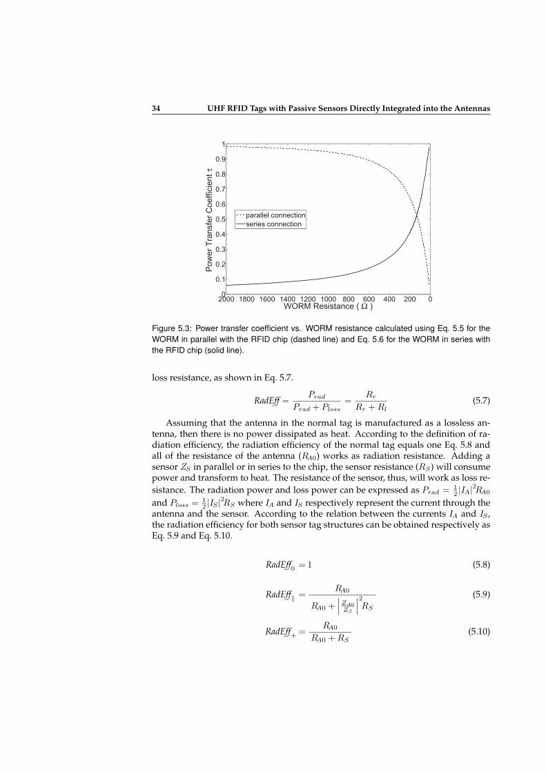
34 UHF RFID Tags with Passive Sensors Directly Integrated into the Antennas
02004006008001000120014001600180020000
0.1
0.2
0.3
0.4
0.5
0.6
0.7
0.8
0.9
1
WORM Resistance ( Ω )
Pow
er
Tra
nsfe
r C
oeff
icie
nt
τparallel connection
series connection
Figure 5.3: Power transfer coefficient vs. WORM resistance calculated using Eq. 5.5 for theWORM in parallel with the RFID chip (dashed line) and Eq. 5.6 for the WORM in series withthe RFID chip (solid line).
loss resistance, as shown in Eq. 5.7.
RadEff =Prad
Prad + Ploss=
Rr
Rr +Rl(5.7)
Assuming that the antenna in the normal tag is manufactured as a lossless an-tenna, then there is no power dissipated as heat. According to the definition of ra-diation efficiency, the radiation efficiency of the normal tag equals one Eq. 5.8 andall of the resistance of the antenna (RA0) works as radiation resistance. Adding asensor ZS in parallel or in series to the chip, the sensor resistance (RS) will consumepower and transform to heat. The resistance of the sensor, thus, will work as loss re-sistance. The radiation power and loss power can be expressed as Prad = 1
2 |IA|2RA0
and Ploss =12 |IS |
2RS where IA and IS respectively represent the current through the
antenna and the sensor. According to the relation between the currents IA and IS ,the radiation efficiency for both sensor tag structures can be obtained respectively asEq. 5.9 and Eq. 5.10.
RadEff0 = 1 (5.8)
RadEff∥ =RA0
RA0 +∣∣∣ZA0
ZS
∣∣∣2RS
(5.9)
RadEff+ =RA0
RA0 +RS(5.10)
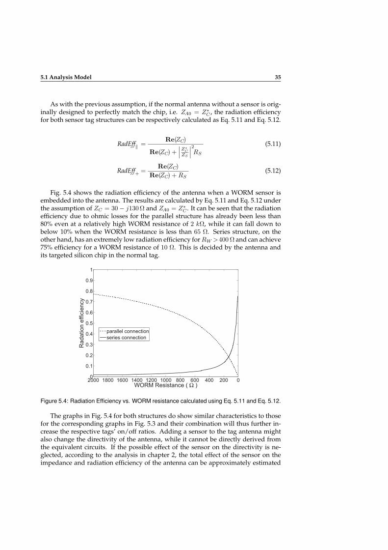
5.1 Analysis Model 35
As with the previous assumption, if the normal antenna without a sensor is orig-inally designed to perfectly match the chip, i.e. ZA0 = Z∗
C , the radiation efficiencyfor both sensor tag structures can be respectively calculated as Eq. 5.11 and Eq. 5.12.
RadEff∥ =Re(ZC)
Re(ZC) +∣∣∣Z∗
C
ZS
∣∣∣2RS
(5.11)
RadEff+ =Re(ZC)
Re(ZC) +RS(5.12)
Fig. 5.4 shows the radiation efficiency of the antenna when a WORM sensor isembedded into the antenna. The results are calculated by Eq. 5.11 and Eq. 5.12 underthe assumption of ZC = 30− j130Ω and ZA0 = Z∗
C . It can be seen that the radiationefficiency due to ohmic losses for the parallel structure has already been less than80% even at a relatively high WORM resistance of 2 kΩ, while it can fall down tobelow 10% when the WORM resistance is less than 65 Ω. Series structure, on theother hand, has an extremely low radiation efficiency for RW >400 Ω and can achieve75% efficiency for a WORM resistance of 10 Ω. This is decided by the antenna andits targeted silicon chip in the normal tag.
02004006008001000120014001600180020000
0.1
0.2
0.3
0.4
0.5
0.6
0.7
0.8
0.9
1
WORM Resistance ( Ω )
Radation e
ffic
iency
parallel connection
series connection
Figure 5.4: Radiation Efficiency vs. WORM resistance calculated using Eq. 5.11 and Eq. 5.12.
The graphs in Fig. 5.4 for both structures do show similar characteristics to thosefor the corresponding graphs in Fig. 5.3 and their combination will thus further in-crease the respective tags’ on/off ratios. Adding a sensor to the tag antenna mightalso change the directivity of the antenna, while it cannot be directly derived fromthe equivalent circuits. If the possible effect of the sensor on the directivity is ne-glected, according to the analysis in chapter 2, the total effect of the sensor on theimpedance and radiation efficiency of the antenna can be approximately estimated
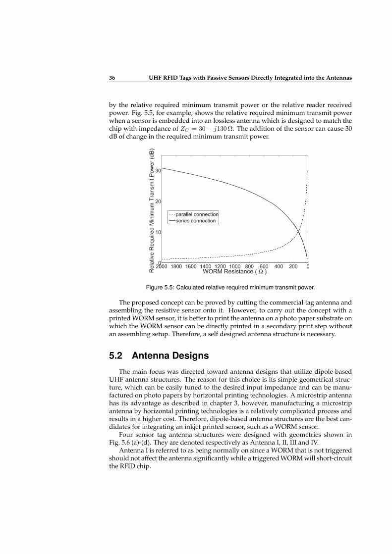
36 UHF RFID Tags with Passive Sensors Directly Integrated into the Antennas
by the relative required minimum transmit power or the relative reader receivedpower. Fig. 5.5, for example, shows the relative required minimum transmit powerwhen a sensor is embedded into an lossless antenna which is designed to match thechip with impedance of ZC = 30 − j130Ω. The addition of the sensor can cause 30dB of change in the required minimum transmit power.
02004006008001000120014001600180020000
10
20
30
WORM Resistance ( Ω )Rela
tive R
equired M
inim
um
Tra
nsm
it P
ow
er
(dB
)
parallel connection
series connection
Figure 5.5: Calculated relative required minimum transmit power.
The proposed concept can be proved by cutting the commercial tag antenna andassembling the resistive sensor onto it. However, to carry out the concept with aprinted WORM sensor, it is better to print the antenna on a photo paper substrate onwhich the WORM sensor can be directly printed in a secondary print step withoutan assembling setup. Therefore, a self designed antenna structure is necessary.
5.2 Antenna Designs
The main focus was directed toward antenna designs that utilize dipole-basedUHF antenna structures. The reason for this choice is its simple geometrical struc-ture, which can be easily tuned to the desired input impedance and can be manu-factured on photo papers by horizontal printing technologies. A microstrip antennahas its advantage as described in chapter 3, however, manufacturing a microstripantenna by horizontal printing technologies is a relatively complicated process andresults in a higher cost. Therefore, dipole-based antenna structures are the best can-didates for integrating an inkjet printed sensor, such as a WORM sensor.
Four sensor tag antenna structures were designed with geometries shown inFig. 5.6 (a)-(d). They are denoted respectively as Antenna I, II, III and IV.
Antenna I is referred to as being normally on since a WORM that is not triggeredshould not affect the antenna significantly while a triggered WORM will short-circuitthe RFID chip.
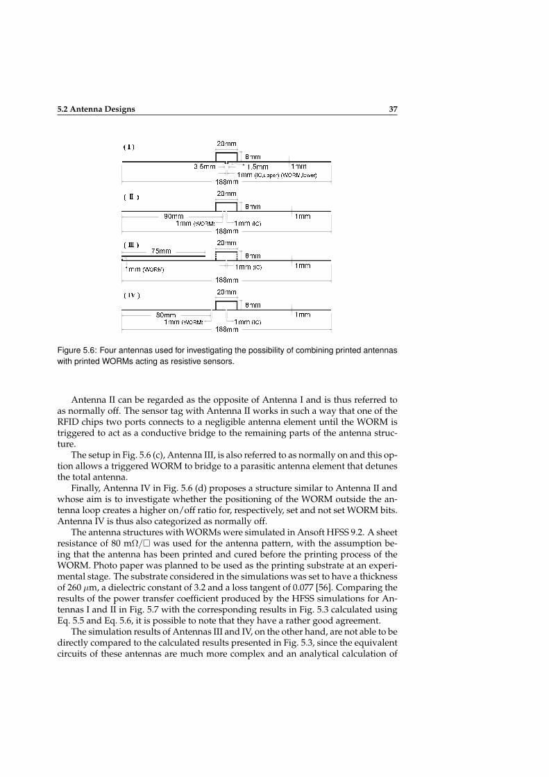
5.2 Antenna Designs 37
Figure 5.6: Four antennas used for investigating the possibility of combining printed antennaswith printed WORMs acting as resistive sensors.
Antenna II can be regarded as the opposite of Antenna I and is thus referred toas normally off. The sensor tag with Antenna II works in such a way that one of theRFID chips two ports connects to a negligible antenna element until the WORM istriggered to act as a conductive bridge to the remaining parts of the antenna struc-ture.
The setup in Fig. 5.6 (c), Antenna III, is also referred to as normally on and this op-tion allows a triggered WORM to bridge to a parasitic antenna element that detunesthe total antenna.
Finally, Antenna IV in Fig. 5.6 (d) proposes a structure similar to Antenna II andwhose aim is to investigate whether the positioning of the WORM outside the an-tenna loop creates a higher on/off ratio for, respectively, set and not set WORM bits.Antenna IV is thus also categorized as normally off.
The antenna structures with WORMs were simulated in Ansoft HFSS 9.2. A sheetresistance of 80 mΩ/ was used for the antenna pattern, with the assumption be-ing that the antenna has been printed and cured before the printing process of theWORM. Photo paper was planned to be used as the printing substrate at an experi-mental stage. The substrate considered in the simulations was set to have a thicknessof 260 µm, a dielectric constant of 3.2 and a loss tangent of 0.077 [56]. Comparing theresults of the power transfer coefficient produced by the HFSS simulations for An-tennas I and II in Fig. 5.7 with the corresponding results in Fig. 5.3 calculated usingEq. 5.5 and Eq. 5.6, it is possible to note that they have a rather good agreement.
The simulation results of Antennas III and IV, on the other hand, are not able to bedirectly compared to the calculated results presented in Fig. 5.3, since the equivalentcircuits of these antennas are much more complex and an analytical calculation of
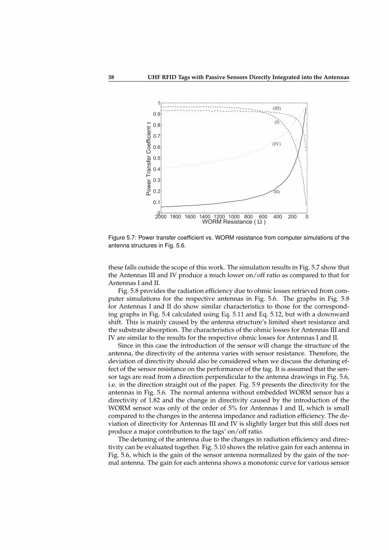
38 UHF RFID Tags with Passive Sensors Directly Integrated into the Antennas
02004006008001000120014001600180020000
0.1
0.2
0.3
0.4
0.5
0.6
0.7
0.8
0.9
1
WORM Resistance ( Ω )
Pow
er
Tra
nsfe
r C
oeff
icie
nt
τ
(III)
(IV)
(I)
(II)
Figure 5.7: Power transfer coefficient vs. WORM resistance from computer simulations of theantenna structures in Fig. 5.6.
these falls outside the scope of this work. The simulation results in Fig. 5.7 show thatthe Antennas III and IV produce a much lower on/off ratio as compared to that forAntennas I and II.
Fig. 5.8 provides the radiation efficiency due to ohmic losses retrieved from com-puter simulations for the respective antennas in Fig. 5.6. The graphs in Fig. 5.8for Antennas I and II do show similar characteristics to those for the correspond-ing graphs in Fig. 5.4 calculated using Eq. 5.11 and Eq. 5.12, but with a downwardshift. This is mainly caused by the antenna structure’s limited sheet resistance andthe substrate absorption. The characteristics of the ohmic losses for Antennas III andIV are similar to the results for the respective ohmic losses for Antennas I and II.
Since in this case the introduction of the sensor will change the structure of theantenna, the directivity of the antenna varies with sensor resistance. Therefore, thedeviation of directivity should also be considered when we discuss the detuning ef-fect of the sensor resistance on the performance of the tag. It is assumed that the sen-sor tags are read from a direction perpendicular to the antenna drawings in Fig. 5.6,i.e. in the direction straight out of the paper. Fig. 5.9 presents the directivity for theantennas in Fig. 5.6. The normal antenna without embedded WORM sensor has adirectivity of 1.82 and the change in directivity caused by the introduction of theWORM sensor was only of the order of 5% for Antennas I and II, which is smallcompared to the changes in the antenna impedance and radiation efficiency. The de-viation of directivity for Antennas III and IV is slightly larger but this still does notproduce a major contribution to the tags’ on/off ratio.
The detuning of the antenna due to the changes in radiation efficiency and direc-tivity can be evaluated together. Fig. 5.10 shows the relative gain for each antenna inFig. 5.6, which is the gain of the sensor antenna normalized by the gain of the nor-mal antenna. The gain for each antenna shows a monotonic curve for various sensor
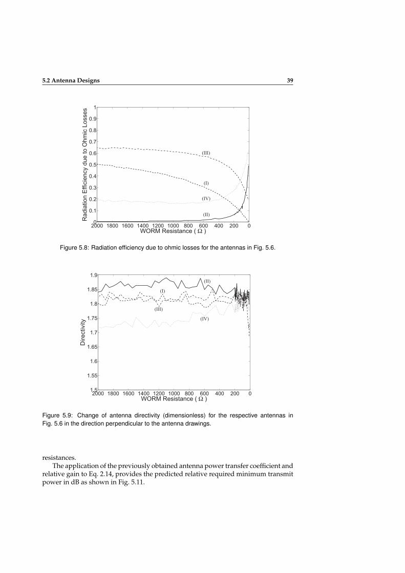
5.2 Antenna Designs 39
02004006008001000120014001600180020000
0.1
0.2
0.3
0.4
0.5
0.6
0.7
0.8
0.9
1
WORM Resistance ( Ω )
Radia
tion E
ffic
iency d
ue t
o O
hm
ic L
osses
(II)
(IV)
(III)
(I)
Figure 5.8: Radiation efficiency due to ohmic losses for the antennas in Fig. 5.6.
02004006008001000120014001600180020001.5
1.55
1.6
1.65
1.7
1.75
1.8
1.85
1.9
WORM Resistance ( Ω )
Directivity
(III)
(I)
(IV)
(II)
Figure 5.9: Change of antenna directivity (dimensionless) for the respective antennas inFig. 5.6 in the direction perpendicular to the antenna drawings.
resistances.The application of the previously obtained antenna power transfer coefficient and
relative gain to Eq. 2.14, provides the predicted relative required minimum transmitpower in dB as shown in Fig. 5.11.
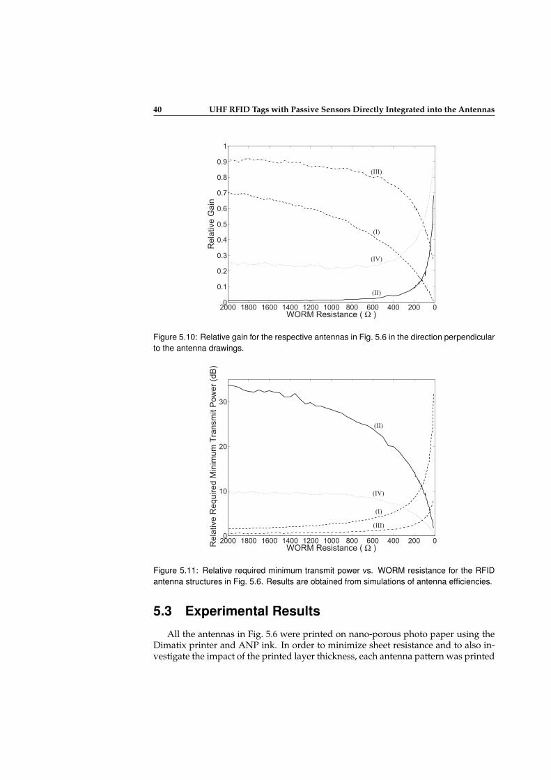
40 UHF RFID Tags with Passive Sensors Directly Integrated into the Antennas
02004006008001000120014001600180020000
0.1
0.2
0.3
0.4
0.5
0.6
0.7
0.8
0.9
1
WORM Resistance ( Ω )
Rela
tive G
ain
(III)
(I)
(II)
(IV)
Figure 5.10: Relative gain for the respective antennas in Fig. 5.6 in the direction perpendicularto the antenna drawings.
02004006008001000120014001600180020000
10
20
30
WORM Resistance ( Ω )Rela
tive R
equired M
inim
um
Tra
nsm
it P
ow
er
(dB
)
(II)
(IV)
(I)
(III)
Figure 5.11: Relative required minimum transmit power vs. WORM resistance for the RFIDantenna structures in Fig. 5.6. Results are obtained from simulations of antenna efficiencies.
5.3 Experimental Results
All the antennas in Fig. 5.6 were printed on nano-porous photo paper using theDimatix printer and ANP ink. In order to minimize sheet resistance and to also in-vestigate the impact of the printed layer thickness, each antenna pattern was printed
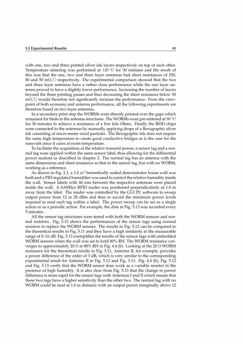
5.3 Experimental Results 41
with one, two and three printed silver ink layers respectively on top of each other.Temperature sintering was performed at 120 C for 30 minutes and the result ofthis was that the one, two and three layer antennas had sheet resistances of 250,80 and 50 mΩ/ respectively. The experimental comparison showed that the twoand three layer antennas have a rather close performance while the one layer an-tenna proved to have a slightly lower performance. Increasing the number of layersbeyond the three printing passes and thus decreasing the sheet resistance below 50mΩ/ would therefore not significantly increase the performance. From the view-point of both economy and antenna performance, all the following experiments aretherefore based on two layer antennas.
In a secondary print step the WORMs were directly printed over the gaps whichremained for them in the antenna structures. The WORMs were pre-sintered at 90 Cfor 30 minutes to achieve a resistance of a few kilo Ohms. Finally the RFID chipswere connected to the antennas by manually applying drops of a flexographic silverink consisting of micro-meter sized particles. The flexographic ink does not requirethe same high temperature to create good conductive bridges as is the case for thenano-ink since it cures at room temperature.
To facilitate the acquisition of the relative transmit power, a sensor tag and a nor-mal tag were applied within the same sensor label, thus allowing for the differentialpower readout as described in chapter 2. The normal tag has an antenna with thesame dimensions and sheet resistance as that in the sensor tag, but with no WORM,working as a reference.
As shown in Fig. 2.1, a 1.0 m2 hermetically sealed demonstrator house wall wasbuilt and a PID-regulated humidifier was used to control the relative humidity insidethe wall. Sensor labels with 40 mm between the respective antennas were placedinside the wall. A SAMSys RFID reader was positioned perpendicularly at 1.0 maway from the label. The reader was controlled by the GUI PC software to sweepoutput power from 12 to 28 dBm and thus to record the minimum power levelsrequired to read each tag within a label. The power sweep can be set as a singleaction or as a periodic action. For example, the data in Fig. 5.13 was recorded every5 minutes.
All the sensor tag structures were tested with both the WORM sensors and nor-mal resistors. Fig. 5.12 shows the performances of the sensor tags using normalresistors to replace the WORM sensors. The results in Fig. 5.12 can be compared tothe theoretical results in Fig. 5.11 and they have a high similarity in the measurablerange of 0–16 dB. Fig. 5.13 exemplifies the results of the sensor tags with embeddedWORM sensors when the wall was set to hold 80% RH. The WORM resistance con-verges to approximately 20 Ω at 80% RH in Fig. 4.4 (b). Looking at the 20 Ω WORMresistance for the theoretical results in Fig. 5.11, Antenna II, for example, providesa power difference of the order of 3 dB, which is very similar to the correspondingexperimental result for Antenna II in Fig. 5.12 and Fig. 5.13. Fig. 4.4 (b), Fig. 5.12and Fig. 5.13 verify that the WORM sensor does work as a variable resistor in thepresence of high humidity. It is also clear from Fig. 5.13 that the change in powerdifference is more rapid for the sensor tags with Antennas I and II which means thatthese two tags have a higher sensitivity than the other two. The normal tag with noWORM could be read at 1.0 m distance with an output power marginally above 12
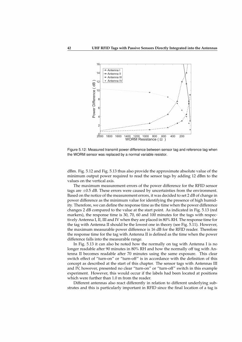
42 UHF RFID Tags with Passive Sensors Directly Integrated into the Antennas
2004006008001000120014001600180020000
2
4
6
8
10
12
14
16
WORM Resistance ( Ω )
Pow
er
Diffe
rence (
dB
)
Antenna I
Antenna II
Antenna III
Antenna IV
Figure 5.12: Measured transmit power difference between sensor tag and reference tag whenthe WORM sensor was replaced by a normal variable resistor.
dBm. Fig. 5.12 and Fig. 5.13 thus also provide the approximate absolute value of theminimum output power required to read the sensor tags by adding 12 dBm to thevalues on the vertical axis.
The maximum measurement errors of the power difference for the RFID sensortags are ±0.5 dB. These errors were caused by uncertainties from the environment.Based on the notice of the measurement errors, it was decided to set 2 dB of change inpower difference as the minimum value for identifying the presence of high humid-ity. Therefore, we can define the response time as the time when the power differencechanges 2 dB compared to the value at the start point. As indicated in Fig. 5.13 (redmarkers), the response time is 30, 70, 60 and 100 minutes for the tags with respec-tively Antenna I, II, III and IV when they are placed in 80% RH. The response time forthe tag with Antenna II should be the lowest one in theory (see Fig. 5.11). However,the maximum measurable power difference is 16 dB for the RFID reader. Thereforethe response time for the tag with Antenna II is defined as the time when the powerdifference falls into the measurable range.
In Fig. 5.13 it can also be noted how the normally on tag with Antenna I is nolonger readable after 90 minutes in 80% RH and how the normally off tag with An-tenna II becomes readable after 70 minutes using the same exposure. This clearswitch effect of “turn-on” or “turn-off” is in accordance with the definition of thisconcept as described at the start of this chapter. The sensor tags with Antennas IIIand IV, however, presented no clear “turn-on” or “turn-off” switch in this exampleexperiment. However, this would occur if the labels had been located at positionswhich were further than 1.0 m from the reader.
Different antennas also react differently in relation to different underlying sub-strates and this is particularly important in RFID since the final location of a tag is
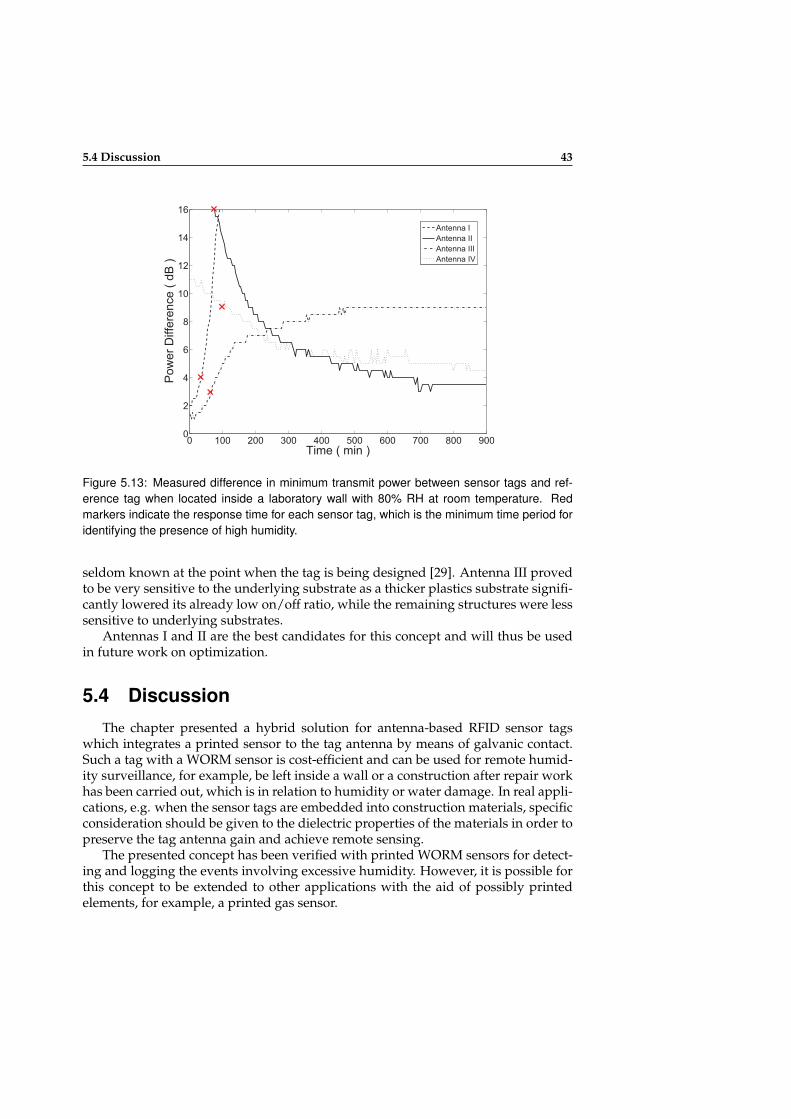
5.4 Discussion 43
0 100 200 300 400 500 600 700 800 9000
2
4
6
8
10
12
14
16
Time ( min )
Pow
er
Diffe
rence (
dB
)
Antenna I
Antenna II
Antenna III
Antenna IV
×
××
×
Figure 5.13: Measured difference in minimum transmit power between sensor tags and ref-erence tag when located inside a laboratory wall with 80% RH at room temperature. Redmarkers indicate the response time for each sensor tag, which is the minimum time period foridentifying the presence of high humidity.
seldom known at the point when the tag is being designed [29]. Antenna III provedto be very sensitive to the underlying substrate as a thicker plastics substrate signifi-cantly lowered its already low on/off ratio, while the remaining structures were lesssensitive to underlying substrates.
Antennas I and II are the best candidates for this concept and will thus be usedin future work on optimization.
5.4 Discussion
The chapter presented a hybrid solution for antenna-based RFID sensor tagswhich integrates a printed sensor to the tag antenna by means of galvanic contact.Such a tag with a WORM sensor is cost-efficient and can be used for remote humid-ity surveillance, for example, be left inside a wall or a construction after repair workhas been carried out, which is in relation to humidity or water damage. In real appli-cations, e.g. when the sensor tags are embedded into construction materials, specificconsideration should be given to the dielectric properties of the materials in order topreserve the tag antenna gain and achieve remote sensing.
The presented concept has been verified with printed WORM sensors for detect-ing and logging the events involving excessive humidity. However, it is possible forthis concept to be extended to other applications with the aid of possibly printedelements, for example, a printed gas sensor.

44
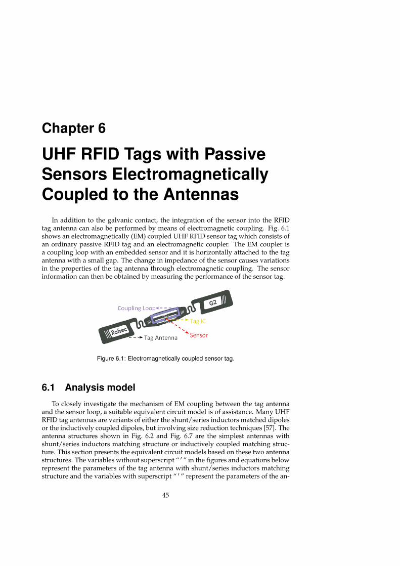
Chapter 6
UHF RFID Tags with PassiveSensors ElectromagneticallyCoupled to the Antennas
In addition to the galvanic contact, the integration of the sensor into the RFIDtag antenna can also be performed by means of electromagnetic coupling. Fig. 6.1shows an electromagnetically (EM) coupled UHF RFID sensor tag which consists ofan ordinary passive RFID tag and an electromagnetic coupler. The EM coupler isa coupling loop with an embedded sensor and it is horizontally attached to the tagantenna with a small gap. The change in impedance of the sensor causes variationsin the properties of the tag antenna through electromagnetic coupling. The sensorinformation can then be obtained by measuring the performance of the sensor tag.
Figure 6.1: Electromagnetically coupled sensor tag.
6.1 Analysis model
To closely investigate the mechanism of EM coupling between the tag antennaand the sensor loop, a suitable equivalent circuit model is of assistance. Many UHFRFID tag antennas are variants of either the shunt/series inductors matched dipolesor the inductively coupled dipoles, but involving size reduction techniques [57]. Theantenna structures shown in Fig. 6.2 and Fig. 6.7 are the simplest antennas withshunt/series inductors matching structure or inductively coupled matching struc-ture. This section presents the equivalent circuit models based on these two antennastructures. The variables without superscript “ ′ ” in the figures and equations belowrepresent the parameters of the tag antenna with shunt/series inductors matchingstructure and the variables with superscript “ ′ ” represent the parameters of the an-
45
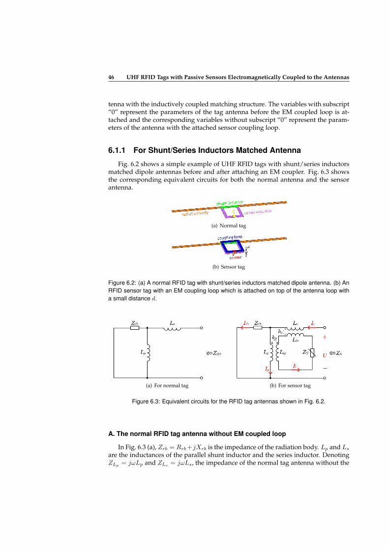
46 UHF RFID Tags with Passive Sensors Electromagnetically Coupled to the Antennas
tenna with the inductively coupled matching structure. The variables with subscript“0” represent the parameters of the tag antenna before the EM coupled loop is at-tached and the corresponding variables without subscript “0” represent the param-eters of the antenna with the attached sensor coupling loop.
6.1.1 For Shunt/Series Inductors Matched Antenna
Fig. 6.2 shows a simple example of UHF RFID tags with shunt/series inductorsmatched dipole antennas before and after attaching an EM coupler. Fig. 6.3 showsthe corresponding equivalent circuits for both the normal antenna and the sensorantenna.
(a) Normal tag
(b) Sensor tag
Figure 6.2: (a) A normal RFID tag with shunt/series inductors matched dipole antenna. (b) AnRFID sensor tag with an EM coupling loop which is attached on top of the antenna loop witha small distance d.
(a) For normal tag (b) For sensor tag
Figure 6.3: Equivalent circuits for the RFID tag antennas shown in Fig. 6.2.
A. The normal RFID tag antenna without EM coupled loop
In Fig. 6.3 (a), Zrb = Rrb+jXrb is the impedance of the radiation body. Lp and Ls
are the inductances of the parallel shunt inductor and the series inductor. DenotingZLp = jωLp and ZLs = jωLs, the impedance of the normal tag antenna without the
6.1 Analysis model 47
EM coupled loop can be expressed as
ZA0 =ZrbZLp
Zrb + ZLp
+ ZLs (6.1)
The resistance and reactance parts of ZA0 can be denoted as RA0 = Re(ZA0) andXA0 = Im(ZA0). Assuming that the antenna is manufactured by a perfect conductor,for the antenna structure in Fig. 6.2 (a), there is no power loss and all of the power istransferred for power radiation. The radiation efficiency is thus equal to one.
RadEff0 = 1 (6.2)
According to the definition of the radiation efficiency (Eq. 5.7), the radiation re-sistance Rr0 and the loss resistance Rl0 of the normal tag antenna can be calculatedfrom
Rr0 =RA0 · RadEff0 = RA0 (6.3)
Rl0 =RA0 · (1− RadEff0) = 0 (6.4)
B. The RFID tag antenna with EM coupled sensor loop
Fig. 6.3 (b) shows the equivalent circuit when the coupling loop is present ontop of the tag antenna. The sensor coupling loop has a self-inductance of (Llp +Lls), where Llp and Lls are the sensor loop’s separated inductances correspondingto Lp and Ls in the antenna loop. kp and ks are the coupling coefficients betweenrespectively Lp and Llp and between Ls and Lls. The mutual inductances are thusMp = kp
√LpLlp and Ms = ks
√LsLls. A sensor ZS = RS + jXS is embedded in the
coupling loop to modulate the properties of the antenna.In Fig. 6.3 (b), the currents through Zrb, Lp, Ls and through the coupling loop
are denoted as Irb, Ip, Is and Il. The voltage at the feed port for connecting the tagIC is denoted as U . The voltages across Zrb, Lp, Ls, Llp, Lls and ZS are respectivelydefined as UZrb
, ULp , ULs , ULlp, ULls
and UZS , through the following expressions:
UZrb=ZrbIrb (6.5)
ULp =ZLpIp + ZMpIl (6.6)
ULs =ZLsIs + ZMsIl (6.7)
ULlp=ZLlp
Il + ZMpIp (6.8)
ULls=ZLls
Il + ZMsIs (6.9)
UZS =ZSIl (6.10)
where ZLlp=jωLlp, ZLls
=jωLls, ZMp =jωMp, ZMs =jωMs.
Based upon Fig. 6.3 (b), the following relations between the voltages and the

48 UHF RFID Tags with Passive Sensors Electromagnetically Coupled to the Antennas
currents can be obtained:
UZrb=ULp = U − ULs (6.11)
0 =ULlp+ ULls
+ UZS(6.12)
Is = Irb + Ip (6.13)
The relations between Irb, Ip, Il and Is are derived from Eq. 6.5-6.13, as follows:
Ip =AIs (6.14)
Il =BIs (6.15)
Irb = (1−A)Is (6.16)
where,
A=TZrb + ZMpZMs
TZrb + TZLp − Z2Mp
B =− 1
T(AZMp + ZMs)
T =ZLlp+ ZLls
+ ZS
The impedance of the antenna with EM coupled loop can be written as a function(Eq. 6.17) of the sensor impedance ZS .
ZA=U
Is=
ULp+ULs
Is=ZLs+AZLp+B(ZMp+ZMs) (6.17)
The resistance and reactance part of ZA can be further denoted as RA = Re(ZA),XA = Im(ZA).
In Fig. 6.3 (b), the power dissipated as radiation (Prad) and the power dissipatedas heat (Ploss) can be given by
Prad = PZrb=
1
2|Irb|2 Rrb (6.18)
Ploss = PZS =1
2| Il |2 RS (6.19)
The radiation efficiency of the antenna with EM coupled loop is then obtainedas:
RadEff =Prad
Prad + Ploss=
|1−A|2Rrb
|1−A|2Rrb + |B|2RS
(6.20)
6.1 Analysis model 49
Therefore, the radiation resistance and loss resistance can be calculated from
Rr =RA · RadEff (6.21)
Rl =RA · (1− RadEff) (6.22)
C. Comparison between equivalent circuit model and full-wave simulation
The antenna shown in Fig. 6.2 (a) was adjusted to match the tag IC, Alien Higgs-4, which has an input impedance of (21 − j191) Ω at 868 MHz [58]. The impedanceof the antenna can be approximated by the equivalent circuit shown in Fig. 6.3 (a).The equivalent circuit parameters can be found by fitting Eq. 6.1 to the simulation ofthe antenna in the considered frequency range. The coupling loop has an structurewhich is exactly the same as the loop in the dipole antenna. Thus, the equivalentcircuit parameters for the coupling loop in Fig. 6.3 (b) are Llp = Lp and Lls = Ls.The coupling coefficients can be calculated by means of a simulation of the couplingbetween the two loops (where the simulated coupling coefficient between two loopsis denoted as k). In our case, the basic shapes of the antenna loop and the couplingloop are identical and the distance between them is uniform, thus the coupling coef-ficients kp and ks are equal k (kp = ks = k). The coupling coefficient is determinedby the distance between the loops and the size of the loops. For the antenna in thiscase, it was observed from the simulations that when the distance d between the twoloops is 100, 300, 500 µm the coupling coefficient k is respectively 0.93, 0.81, 0.72.
By using these parameters, the antenna impedance (Eq. 6.17) and the radiationefficiency (Eq. 6.20) are easily obtained for various sensor impedances.
(1) ZS is resistive, i.e. ZS = RS
When the sensor is purely resistive and RS changes from 0 to 107 Ω, the corre-sponding antenna impedance ZA, radiation resistance Rr, loss resistance Rl and ra-diation efficiency are calculated using the equivalent circuit model described aboveand simulated in HFSS. The results are plotted in Fig. 6.4(a), 6.4(b) and 6.4(c), wherethe respective results calculated from the model and simulated in HFSS are in goodagreement. When the coupling loop is open or when the sensor has a high resistance,the impedance and radiation efficiency of the sensor antenna are approximatelyequal to those of the normal antenna and the sensor antenna has a good match withthe tag IC. When the coupling loop is closed or when the sensor has an extremely lowresistance, the radiation efficiency of the sensor antenna is about one, but there is stilla mismatch with the IC. Apart from these two extreme situations, it can be noted thatthe varied RS does result in changes in the antenna parameters. The imaginary partof the antenna impedance XA increases when RS changes from zero to tens of Mega-Ohm, while the real part of the antenna impedance RA has a peak value. RA is alsothe sum of the monotonously increased Rr and the non-monotonically changed Rl.The radiation resistance Rr monotonously increases with RS which mainly occurs inthe range of RS from 10 Ω to 10 kΩ and Rr remains flat outside this range. The lossresistance Rl is close to zero when RS is less than 1 Ω or larger than 100 kΩ and hasa peak value when the sensor resistance RS = 200 Ω. Thus, the radiation efficiencyhas a minimum value at RS = 70 Ω. The calculated power transfer coefficient τ is
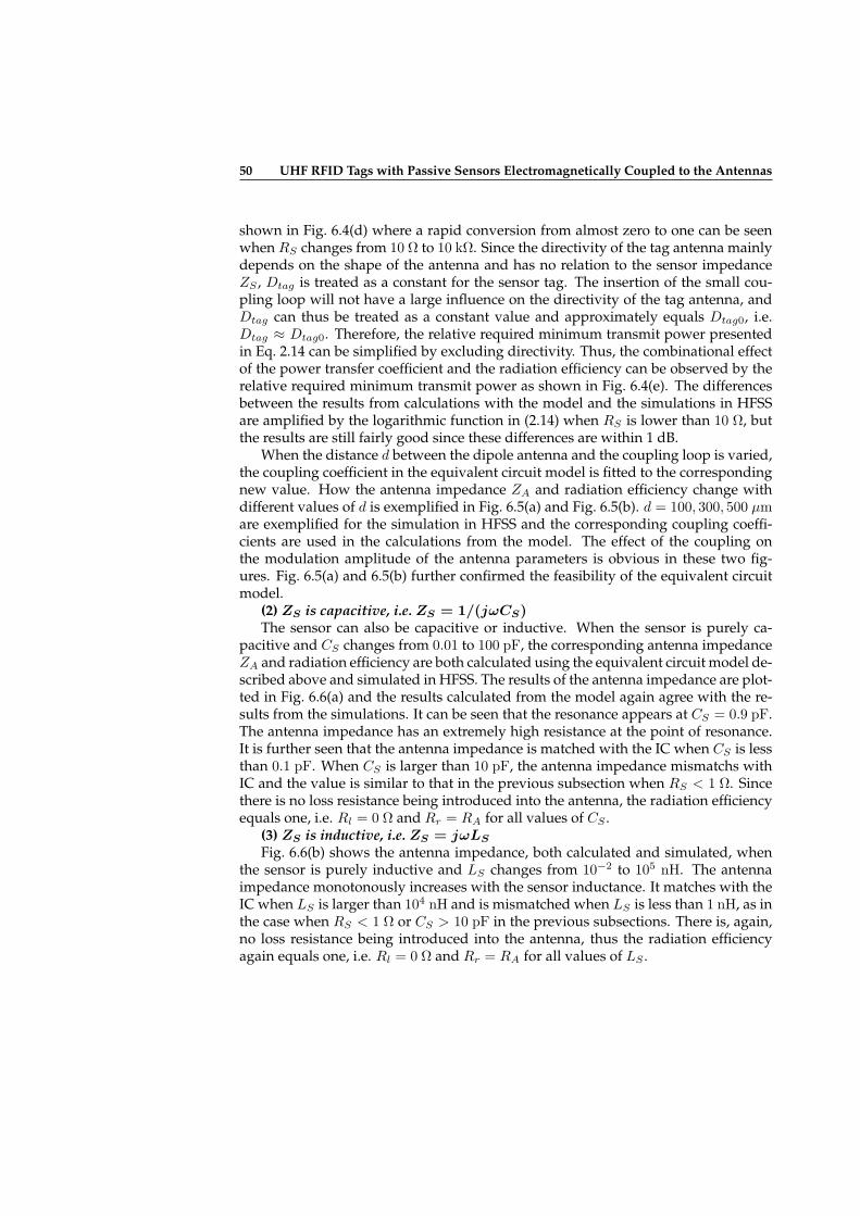
50 UHF RFID Tags with Passive Sensors Electromagnetically Coupled to the Antennas
shown in Fig. 6.4(d) where a rapid conversion from almost zero to one can be seenwhen RS changes from 10 Ω to 10 kΩ. Since the directivity of the tag antenna mainlydepends on the shape of the antenna and has no relation to the sensor impedanceZS , Dtag is treated as a constant for the sensor tag. The insertion of the small cou-pling loop will not have a large influence on the directivity of the tag antenna, andDtag can thus be treated as a constant value and approximately equals Dtag0, i.e.Dtag ≈ Dtag0. Therefore, the relative required minimum transmit power presentedin Eq. 2.14 can be simplified by excluding directivity. Thus, the combinational effectof the power transfer coefficient and the radiation efficiency can be observed by therelative required minimum transmit power as shown in Fig. 6.4(e). The differencesbetween the results from calculations with the model and the simulations in HFSSare amplified by the logarithmic function in (2.14) when RS is lower than 10 Ω, butthe results are still fairly good since these differences are within 1 dB.
When the distance d between the dipole antenna and the coupling loop is varied,the coupling coefficient in the equivalent circuit model is fitted to the correspondingnew value. How the antenna impedance ZA and radiation efficiency change withdifferent values of d is exemplified in Fig. 6.5(a) and Fig. 6.5(b). d = 100, 300, 500 µmare exemplified for the simulation in HFSS and the corresponding coupling coeffi-cients are used in the calculations from the model. The effect of the coupling onthe modulation amplitude of the antenna parameters is obvious in these two fig-ures. Fig. 6.5(a) and 6.5(b) further confirmed the feasibility of the equivalent circuitmodel.
(2) ZS is capacitive, i.e. ZS = 1/(jωCS)The sensor can also be capacitive or inductive. When the sensor is purely ca-
pacitive and CS changes from 0.01 to 100 pF, the corresponding antenna impedanceZA and radiation efficiency are both calculated using the equivalent circuit model de-scribed above and simulated in HFSS. The results of the antenna impedance are plot-ted in Fig. 6.6(a) and the results calculated from the model again agree with the re-sults from the simulations. It can be seen that the resonance appears at CS = 0.9 pF.The antenna impedance has an extremely high resistance at the point of resonance.It is further seen that the antenna impedance is matched with the IC when CS is lessthan 0.1 pF. When CS is larger than 10 pF, the antenna impedance mismatchs withIC and the value is similar to that in the previous subsection when RS < 1 Ω. Sincethere is no loss resistance being introduced into the antenna, the radiation efficiencyequals one, i.e. Rl = 0 Ω and Rr = RA for all values of CS .
(3) ZS is inductive, i.e. ZS = jωLS
Fig. 6.6(b) shows the antenna impedance, both calculated and simulated, whenthe sensor is purely inductive and LS changes from 10−2 to 105 nH. The antennaimpedance monotonously increases with the sensor inductance. It matches with theIC when LS is larger than 104 nH and is mismatched when LS is less than 1 nH, as inthe case when RS < 1 Ω or CS > 10 pF in the previous subsections. There is, again,no loss resistance being introduced into the antenna, thus the radiation efficiencyagain equals one, i.e. Rl = 0 Ω and Rr = RA for all values of LS .
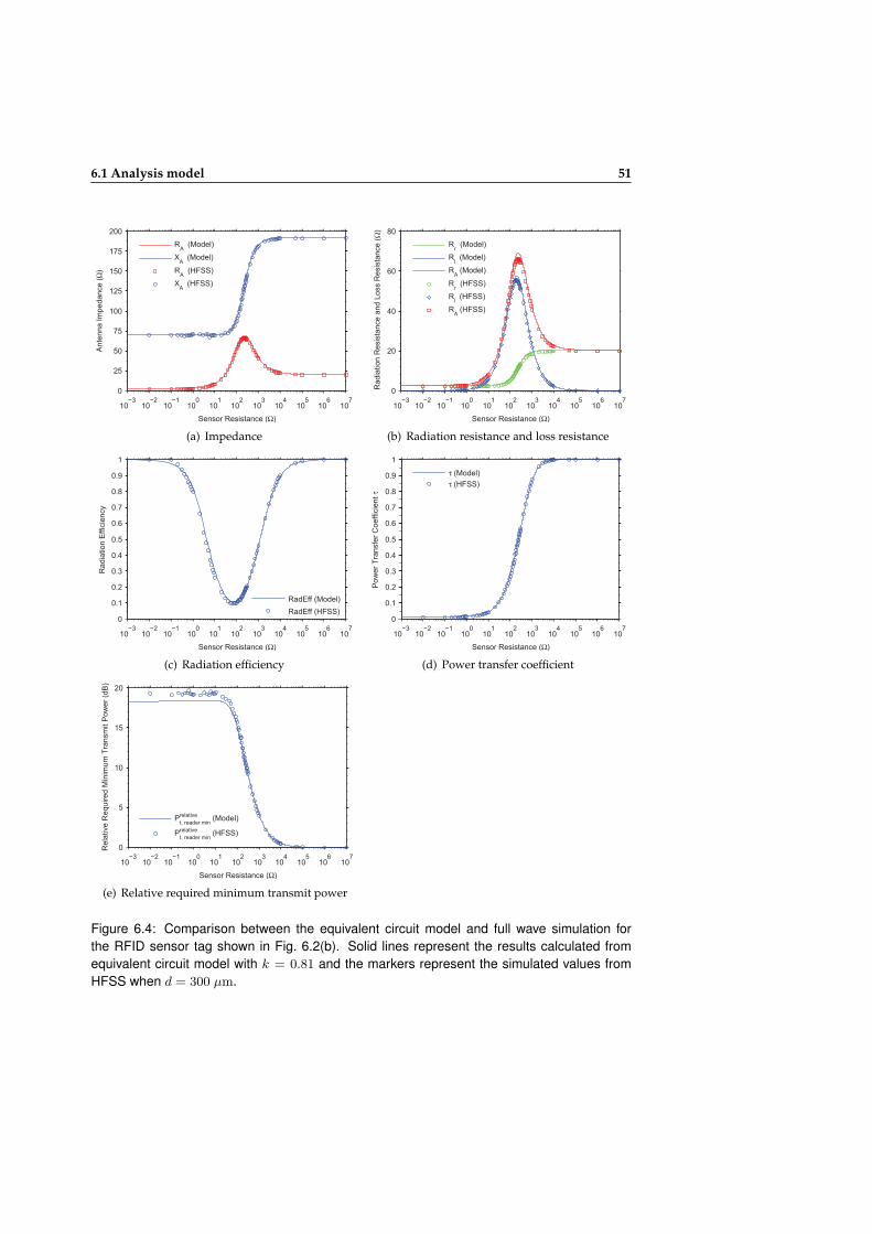
6.1 Analysis model 51
10−3
10−2
10−1
100
101
102
103
104
105
106
107
0
25
50
75
100
125
150
175
200
Sensor Resistance (Ω)
Ante
nna I
mpedance (
Ω)
RA (Model)
XA (Model)
RA (HFSS)
XA (HFSS)
(a) Impedance
10−3
10−2
10−1
100
101
102
103
104
105
106
107
0
20
40
60
80
Sensor Resistance (Ω)
Radia
tion R
esis
tance a
nd L
oss R
esis
tance (
Ω)
Rr (Model)
Rl (Model)
RA (Model)
Rr (HFSS)
Rl (HFSS)
RA (HFSS)
(b) Radiation resistance and loss resistance
10−3
10−2
10−1
100
101
102
103
104
105
106
107
0
0.1
0.2
0.3
0.4
0.5
0.6
0.7
0.8
0.9
1
Sensor Resistance (Ω)
Radia
tion E
ffic
iency
RadEff (Model)
RadEff (HFSS)
(c) Radiation efficiency
10−3
10−2
10−1
100
101
102
103
104
105
106
107
0
0.1
0.2
0.3
0.4
0.5
0.6
0.7
0.8
0.9
1
Sensor Resistance (Ω)
Pow
er
Tra
nsfe
r C
oeff
icie
nt
τ
τ (Model)
τ (HFSS)
(d) Power transfer coefficient
10−3
10−2
10−1
100
101
102
103
104
105
106
107
0
5
10
15
20
Sensor Resistance (Ω)
Rela
tive R
equired M
inim
um
Tra
nsm
it P
ow
er
(dB
)
Prelative
t, reader min (Model)
Prelative
t, reader min (HFSS)
(e) Relative required minimum transmit power
Figure 6.4: Comparison between the equivalent circuit model and full wave simulation forthe RFID sensor tag shown in Fig. 6.2(b). Solid lines represent the results calculated fromequivalent circuit model with k = 0.81 and the markers represent the simulated values fromHFSS when d = 300 µm.
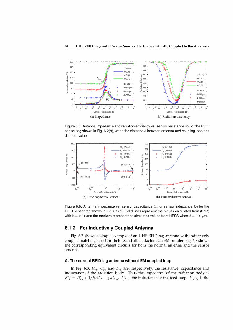
52 UHF RFID Tags with Passive Sensors Electromagnetically Coupled to the Antennas
10−3
10−2
10−1
100
101
102
103
104
105
106
107
0
25
50
75
100
125
150
175
200
Sensor Resistance (Ω)
Ante
nna I
mpedance (
Ω)
XA
RA
(HFSS)
d=100µm
d=300µm
d=500µm
(Model)
k=0.93
k=0.81
k=0.72
(a) Impedance
10−3
10−2
10−1
100
101
102
103
104
105
106
107
0
0.1
0.2
0.3
0.4
0.5
0.6
0.7
0.8
0.9
1
Sensor Resistance (Ω)
Radia
tion E
ffic
iency
(HFSS)
d=100µm
d=300µm
d=500µm
(Model)
k=0.93
k=0.81
k=0.72
(b) Radiation efficiency
Figure 6.5: Antenna impedance and radiation efficiency vs. sensor resistance RS for the RFIDsensor tag shown in Fig. 6.2(b), when the distance d between antenna and coupling loop hasdifferent values.
10−2
10−1
100
101
102
−1000
−500
0
500
1000
1500
2000
Sensor Capacitance (pF)
Ante
nna I
mpedance (
Ω)
RA (Model)
ZA (Model)
RA (HFSS)
XA (HFSS)
(0.01,19.9)
(0.01,193)
(100,1.98)
(100,68.3)
(a) Pure capacitive sensor
10−2
10−1
100
101
102
103
104
105
0
25
50
75
100
125
150
175
200
Sensor Inductance (nH)
Ante
nna I
mpedance (
Ω)
RA (Model)
ZA (Model)
RA (HFSS)
XA (HFSS)
(b) Pure inductive sensor
Figure 6.6: Antenna impedance vs. sensor capacitance CS or sensor inductance LS for theRFID sensor tag shown in Fig. 6.2(b). Solid lines represent the results calculated from (6.17)with k = 0.81 and the markers represent the simulated values from HFSS when d = 300 µm.
6.1.2 For Inductively Coupled Antenna
Fig. 6.7 shows a simple example of an UHF RFID tag antenna with inductivelycoupled matching structure, before and after attaching an EM coupler. Fig. 6.8 showsthe corresponding equivalent circuits for both the normal antenna and the sensorantenna.
A. The normal RFID tag antenna without EM coupled loop
In Fig. 6.8, R′rb, C ′
rb and L′rb are, respectively, the resistance, capacitance and
inductance of the radiation body. Thus the impedance of the radiation body isZ ′rb = R′
rb + 1/jωC ′rb + jωL′
rb. L′fl is the inductance of the feed loop. k′rb,fl is the
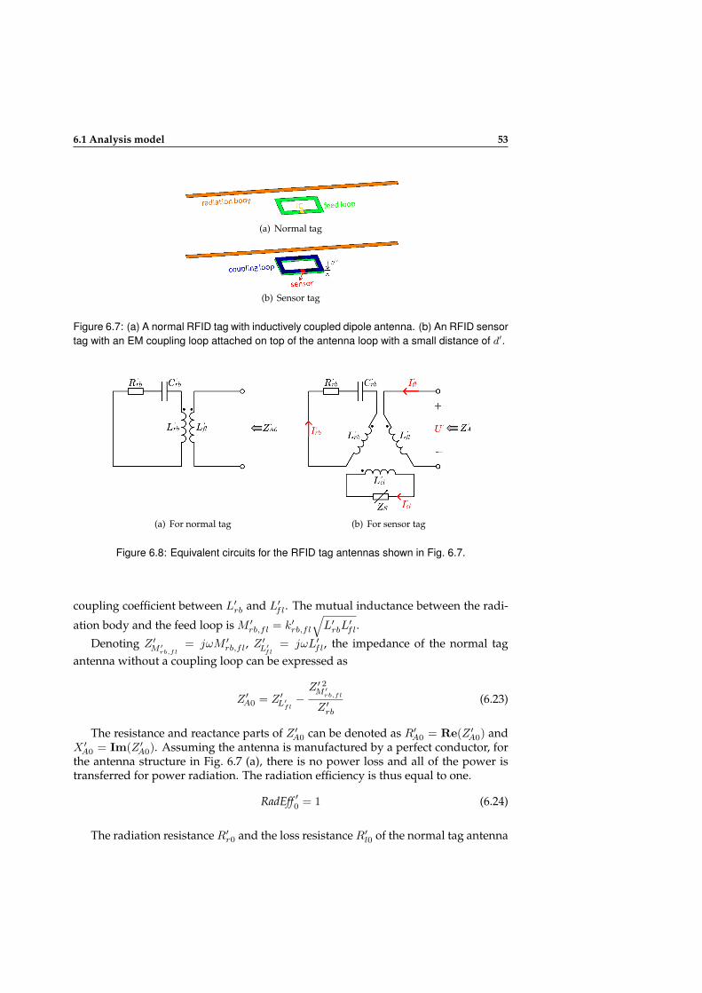
6.1 Analysis model 53
(a) Normal tag
(b) Sensor tag
Figure 6.7: (a) A normal RFID tag with inductively coupled dipole antenna. (b) An RFID sensortag with an EM coupling loop attached on top of the antenna loop with a small distance of d′.
(a) For normal tag (b) For sensor tag
Figure 6.8: Equivalent circuits for the RFID tag antennas shown in Fig. 6.7.
coupling coefficient between L′rb and L′
fl. The mutual inductance between the radi-
ation body and the feed loop is M ′rb,fl = k′rb,fl
√L′rbL
′fl.
Denoting Z ′M ′
rb,fl= jωM ′
rb,fl, Z′L′fl
= jωL′fl, the impedance of the normal tag
antenna without a coupling loop can be expressed as
Z ′A0 = Z ′
L′fl−
Z ′ 2M ′
rb,fl
Z ′rb
(6.23)
The resistance and reactance parts of Z ′A0 can be denoted as R′
A0 = Re(Z ′A0) and
X ′A0 = Im(Z ′
A0). Assuming the antenna is manufactured by a perfect conductor, forthe antenna structure in Fig. 6.7 (a), there is no power loss and all of the power istransferred for power radiation. The radiation efficiency is thus equal to one.
RadEff ′0 = 1 (6.24)
The radiation resistance R′r0 and the loss resistance R′
l0 of the normal tag antenna

54 UHF RFID Tags with Passive Sensors Electromagnetically Coupled to the Antennas
can be calculated from
R′r0 =R′
A0 · RadEff ′0 = R′A0 (6.25)
R′l0 =R′
A0 · (1− RadEff ′0) = 0 (6.26)
B. The RFID tag antenna with EM coupled sensor loop
Fig. 6.8 (b) shows the equivalent circuit when the coupling loop is present ontop of the tag antenna. The coupling loop has an self-inductance of L′
cl. k′rb,cl, k
′fl,cl
are the coupling coefficients between L′rb and L′
cl, L′fl and L′
cl. Thus the mutual
coupling inductances are M ′rb,cl = k′rb,cl
√L′rbL
′cl, M
′fl,cl = k′fl,cl
√L′flL
′cl. A sensor
ZS = RS + jXS is embedded in the coupling loop to modulate the properties of theantenna.
Denoting the currents through the radiation body, the feed loop and the couplingloop as I ′rb, I ′fl and I ′cl, the following relations can be obtained from Fig. 6.8 (b):
0 =Z ′rbI
′rb + Z ′
M ′rb,fl
I ′fl + Z ′M ′
rb,clI ′cl (6.27)
0 = (Z ′L′
cl+ ZS)I
′cl + Z ′
M ′rb,cl
I ′rb + Z ′M ′
fl,clI ′fl (6.28)
U ′ =Z ′L′flI ′fl + Z ′
M ′rb,fl
I ′rb + Z ′M ′
fl,clI ′cl (6.29)
where Z ′L′
rb= jωL′
rb, Z ′L′
cl= jωL′
cl, Z′M ′
rb,cl= jωM ′
rb,cl, Z′M ′
fl,cl= jωM ′
fl,cl.
Then the relations between I ′rb, I ′cl and I ′fl are derived from Eq. 6.27-Eq. 6.28, asfollows:
I ′rb =A′I ′fl (6.30)
I ′cl =B′I ′fl (6.31)
where,
A′ =Z ′M ′
fl,clZ ′M ′
rb,cl− Z ′
M ′rb,fl
(Z ′L′
cl+ ZS)
Z ′rb(Z
′L′
cl+ ZS)− Z ′ 2
M ′rb,cl
B′ =Z ′M ′
rb,flZ ′M ′
rb,cl− Z ′
rbZ′M ′
fl,cl
Z ′rb(Z
′L′
cl+ ZS)− Z ′ 2
M ′rb,cl
The impedance of the antenna with EM couple loop can be written as a function(Eq. 6.32) of the sensor impedance ZS .
Z ′A =
U ′
I ′fl= ZL′
fl+A′Z ′
M ′rb,fl
+B′Z ′M ′
fl,cl(6.32)
The resistance and reactance part of ZA can be further denoted as R′A = Re(Z ′
A),X ′A = Im(Z ′
A).
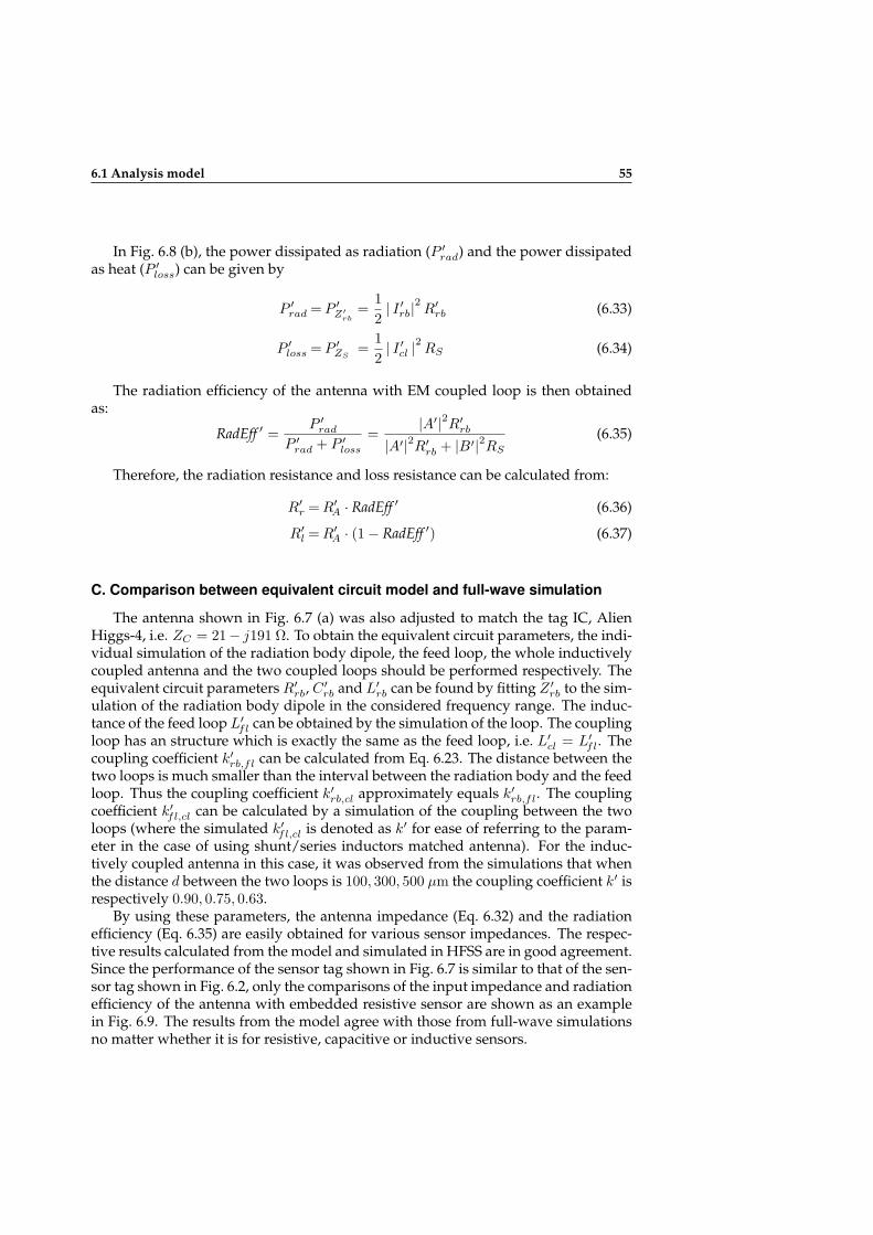
6.1 Analysis model 55
In Fig. 6.8 (b), the power dissipated as radiation (P ′rad) and the power dissipated
as heat (P ′loss) can be given by
P ′rad = P ′
Z′rb
=1
2| I ′rb|
2R′
rb (6.33)
P ′loss = P ′
ZS=
1
2| I ′cl |
2RS (6.34)
The radiation efficiency of the antenna with EM coupled loop is then obtainedas:
RadEff ′ =P ′rad
P ′rad + P ′
loss
=|A′|2R′
rb
|A′|2R′rb + |B′|2RS
(6.35)
Therefore, the radiation resistance and loss resistance can be calculated from:
R′r =R′
A · RadEff ′ (6.36)
R′l =R′
A · (1− RadEff ′) (6.37)
C. Comparison between equivalent circuit model and full-wave simulation
The antenna shown in Fig. 6.7 (a) was also adjusted to match the tag IC, AlienHiggs-4, i.e. ZC = 21− j191 Ω. To obtain the equivalent circuit parameters, the indi-vidual simulation of the radiation body dipole, the feed loop, the whole inductivelycoupled antenna and the two coupled loops should be performed respectively. Theequivalent circuit parameters R′
rb, C ′rb and L′
rb can be found by fitting Z ′rb to the sim-
ulation of the radiation body dipole in the considered frequency range. The induc-tance of the feed loop L′
fl can be obtained by the simulation of the loop. The couplingloop has an structure which is exactly the same as the feed loop, i.e. L′
cl = L′fl. The
coupling coefficient k′rb,fl can be calculated from Eq. 6.23. The distance between thetwo loops is much smaller than the interval between the radiation body and the feedloop. Thus the coupling coefficient k′rb,cl approximately equals k′rb,fl. The couplingcoefficient k′fl,cl can be calculated by a simulation of the coupling between the twoloops (where the simulated k′fl,cl is denoted as k′ for ease of referring to the param-eter in the case of using shunt/series inductors matched antenna). For the induc-tively coupled antenna in this case, it was observed from the simulations that whenthe distance d between the two loops is 100, 300, 500 µm the coupling coefficient k′ isrespectively 0.90, 0.75, 0.63.
By using these parameters, the antenna impedance (Eq. 6.32) and the radiationefficiency (Eq. 6.35) are easily obtained for various sensor impedances. The respec-tive results calculated from the model and simulated in HFSS are in good agreement.Since the performance of the sensor tag shown in Fig. 6.7 is similar to that of the sen-sor tag shown in Fig. 6.2, only the comparisons of the input impedance and radiationefficiency of the antenna with embedded resistive sensor are shown as an examplein Fig. 6.9. The results from the model agree with those from full-wave simulationsno matter whether it is for resistive, capacitive or inductive sensors.
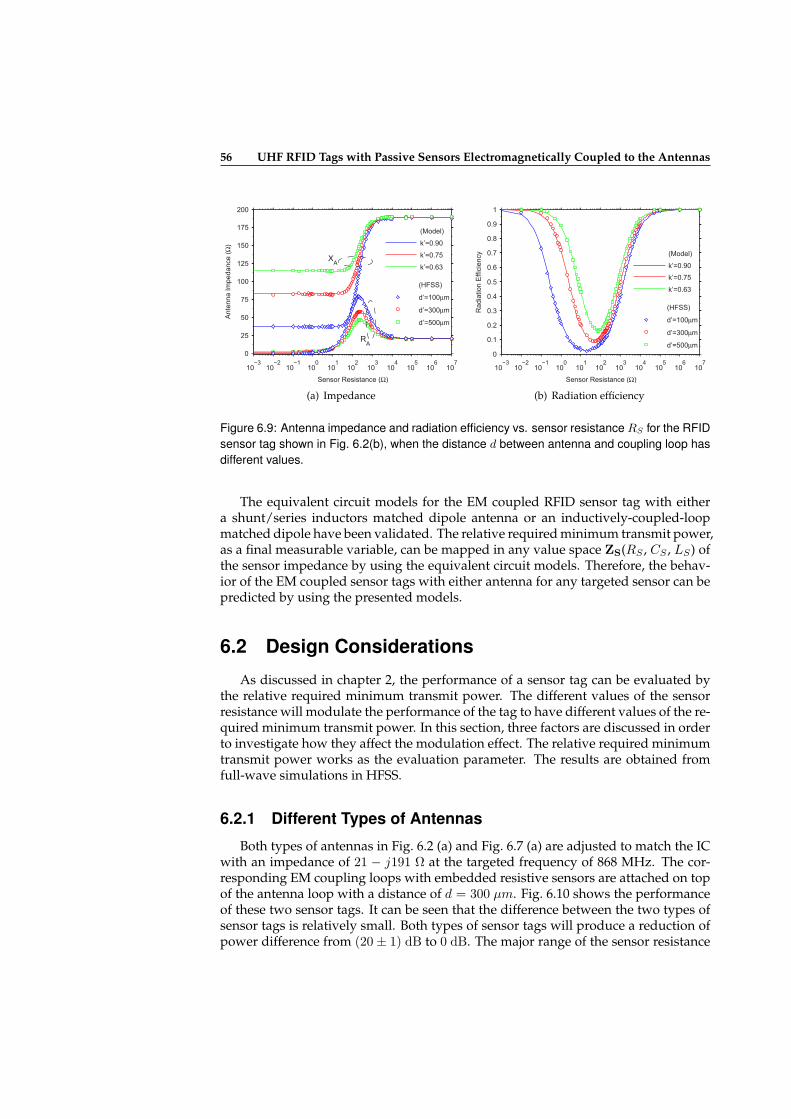
56 UHF RFID Tags with Passive Sensors Electromagnetically Coupled to the Antennas
10−3
10−2
10−1
100
101
102
103
104
105
106
107
0
25
50
75
100
125
150
175
200
Sensor Resistance (Ω)
Ante
nna I
mpedance (
Ω)
XA
RA
(HFSS)
d’=100µm
d’=300µm
d’=500µm
(Model)
k’=0.90
k’=0.75
k’=0.63
(a) Impedance
10−3
10−2
10−1
100
101
102
103
104
105
106
107
0
0.1
0.2
0.3
0.4
0.5
0.6
0.7
0.8
0.9
1
Sensor Resistance (Ω)
Radia
tion E
ffic
iency
(HFSS)
d’=100µm
d’=300µm
d’=500µm
(Model)
k’=0.90
k’=0.75
k’=0.63
(b) Radiation efficiency
Figure 6.9: Antenna impedance and radiation efficiency vs. sensor resistance RS for the RFIDsensor tag shown in Fig. 6.2(b), when the distance d between antenna and coupling loop hasdifferent values.
The equivalent circuit models for the EM coupled RFID sensor tag with eithera shunt/series inductors matched dipole antenna or an inductively-coupled-loopmatched dipole have been validated. The relative required minimum transmit power,as a final measurable variable, can be mapped in any value space ZS(RS , CS , LS) ofthe sensor impedance by using the equivalent circuit models. Therefore, the behav-ior of the EM coupled sensor tags with either antenna for any targeted sensor can bepredicted by using the presented models.
6.2 Design Considerations
As discussed in chapter 2, the performance of a sensor tag can be evaluated bythe relative required minimum transmit power. The different values of the sensorresistance will modulate the performance of the tag to have different values of the re-quired minimum transmit power. In this section, three factors are discussed in orderto investigate how they affect the modulation effect. The relative required minimumtransmit power works as the evaluation parameter. The results are obtained fromfull-wave simulations in HFSS.
6.2.1 Different Types of Antennas
Both types of antennas in Fig. 6.2 (a) and Fig. 6.7 (a) are adjusted to match the ICwith an impedance of 21 − j191 Ω at the targeted frequency of 868 MHz. The cor-responding EM coupling loops with embedded resistive sensors are attached on topof the antenna loop with a distance of d = 300 µm. Fig. 6.10 shows the performanceof these two sensor tags. It can be seen that the difference between the two types ofsensor tags is relatively small. Both types of sensor tags will produce a reduction ofpower difference from (20± 1) dB to 0 dB. The major range of the sensor resistance
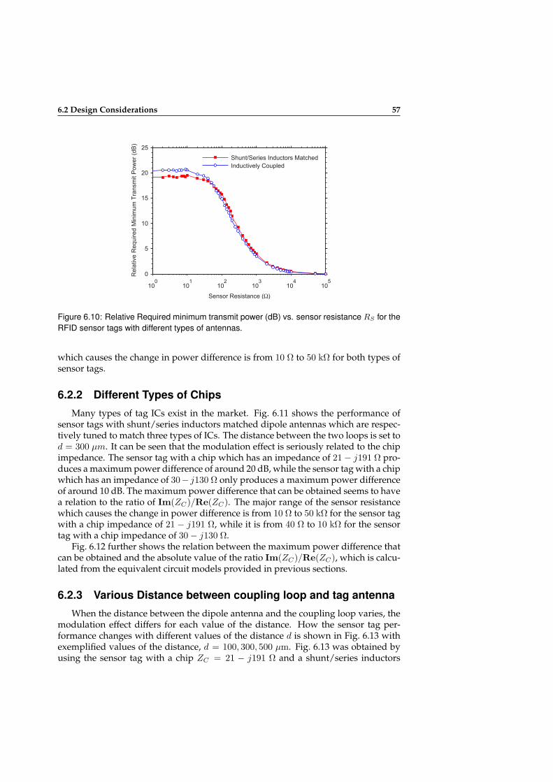
6.2 Design Considerations 57
100
101
102
103
104
105
0
5
10
15
20
25
Sensor Resistance (Ω)
Rela
tive R
equired M
inim
um
Tra
nsm
it P
ow
er
(dB
)
Shunt/Series Inductors Matched
Inductively Coupled
Figure 6.10: Relative Required minimum transmit power (dB) vs. sensor resistance RS for theRFID sensor tags with different types of antennas.
which causes the change in power difference is from 10 Ω to 50 kΩ for both types ofsensor tags.
6.2.2 Different Types of Chips
Many types of tag ICs exist in the market. Fig. 6.11 shows the performance ofsensor tags with shunt/series inductors matched dipole antennas which are respec-tively tuned to match three types of ICs. The distance between the two loops is set tod = 300 µm. It can be seen that the modulation effect is seriously related to the chipimpedance. The sensor tag with a chip which has an impedance of 21− j191 Ω pro-duces a maximum power difference of around 20 dB, while the sensor tag with a chipwhich has an impedance of 30− j130 Ω only produces a maximum power differenceof around 10 dB. The maximum power difference that can be obtained seems to havea relation to the ratio of Im(ZC)/Re(ZC). The major range of the sensor resistancewhich causes the change in power difference is from 10 Ω to 50 kΩ for the sensor tagwith a chip impedance of 21 − j191 Ω, while it is from 40 Ω to 10 kΩ for the sensortag with a chip impedance of 30− j130 Ω.
Fig. 6.12 further shows the relation between the maximum power difference thatcan be obtained and the absolute value of the ratio Im(ZC)/Re(ZC), which is calcu-lated from the equivalent circuit models provided in previous sections.
6.2.3 Various Distance between coupling loop and tag antenna
When the distance between the dipole antenna and the coupling loop varies, themodulation effect differs for each value of the distance. How the sensor tag per-formance changes with different values of the distance d is shown in Fig. 6.13 withexemplified values of the distance, d = 100, 300, 500 µm. Fig. 6.13 was obtained byusing the sensor tag with a chip ZC = 21 − j191 Ω and a shunt/series inductors
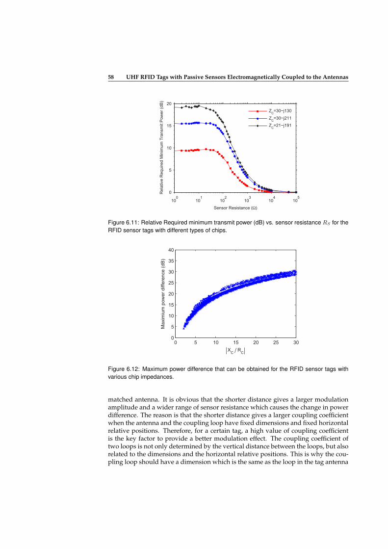
58 UHF RFID Tags with Passive Sensors Electromagnetically Coupled to the Antennas
100
101
102
103
104
105
0
5
10
15
20
Sensor Resistance (Ω)
Rela
tive R
equired M
inim
um
Tra
nsm
it P
ow
er
(dB
)
ZC=30−j130
ZC=30−j211
ZC=21−j191
Figure 6.11: Relative Required minimum transmit power (dB) vs. sensor resistance RS for theRFID sensor tags with different types of chips.
0 5 10 15 20 25 300
5
10
15
20
25
30
35
40
XC
RC
Maxim
ium
pow
er
diffe
rence (
dB
)
|| /
Figure 6.12: Maximum power difference that can be obtained for the RFID sensor tags withvarious chip impedances.
matched antenna. It is obvious that the shorter distance gives a larger modulationamplitude and a wider range of sensor resistance which causes the change in powerdifference. The reason is that the shorter distance gives a larger coupling coefficientwhen the antenna and the coupling loop have fixed dimensions and fixed horizontalrelative positions. Therefore, for a certain tag, a high value of coupling coefficientis the key factor to provide a better modulation effect. The coupling coefficient oftwo loops is not only determined by the vertical distance between the loops, but alsorelated to the dimensions and the horizontal relative positions. This is why the cou-pling loop should have a dimension which is the same as the loop in the tag antenna
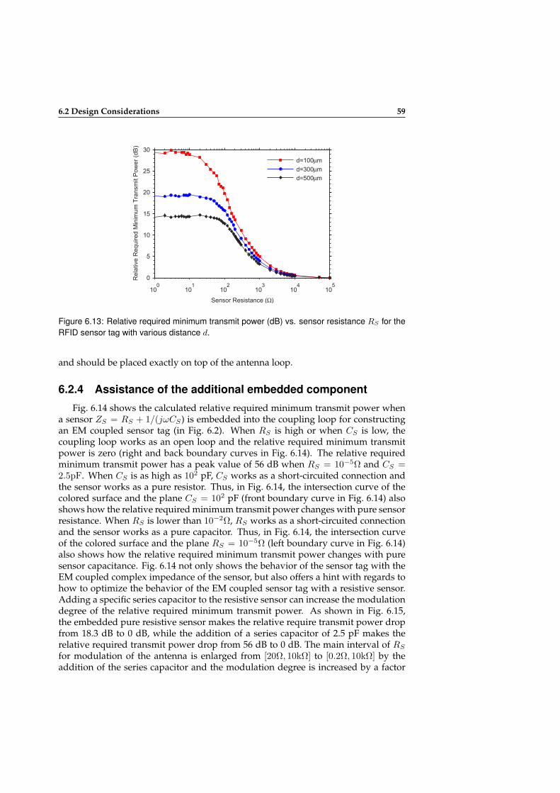
6.2 Design Considerations 59
100
101
102
103
104
105
0
5
10
15
20
25
30
Sensor Resistance (Ω)
Rela
tive R
equired M
inim
um
Tra
nsm
it P
ow
er
(dB
)
d=100µm
d=300µm
d=500µm
Figure 6.13: Relative required minimum transmit power (dB) vs. sensor resistance RS for theRFID sensor tag with various distance d.
and should be placed exactly on top of the antenna loop.
6.2.4 Assistance of the additional embedded component
Fig. 6.14 shows the calculated relative required minimum transmit power whena sensor ZS = RS + 1/(jωCS) is embedded into the coupling loop for constructingan EM coupled sensor tag (in Fig. 6.2). When RS is high or when CS is low, thecoupling loop works as an open loop and the relative required minimum transmitpower is zero (right and back boundary curves in Fig. 6.14). The relative requiredminimum transmit power has a peak value of 56 dB when RS = 10−5Ω and CS =2.5pF. When CS is as high as 102 pF, CS works as a short-circuited connection andthe sensor works as a pure resistor. Thus, in Fig. 6.14, the intersection curve of thecolored surface and the plane CS = 102 pF (front boundary curve in Fig. 6.14) alsoshows how the relative required minimum transmit power changes with pure sensorresistance. When RS is lower than 10−2Ω, RS works as a short-circuited connectionand the sensor works as a pure capacitor. Thus, in Fig. 6.14, the intersection curveof the colored surface and the plane RS = 10−5Ω (left boundary curve in Fig. 6.14)also shows how the relative required minimum transmit power changes with puresensor capacitance. Fig. 6.14 not only shows the behavior of the sensor tag with theEM coupled complex impedance of the sensor, but also offers a hint with regards tohow to optimize the behavior of the EM coupled sensor tag with a resistive sensor.Adding a specific series capacitor to the resistive sensor can increase the modulationdegree of the relative required minimum transmit power. As shown in Fig. 6.15,the embedded pure resistive sensor makes the relative require transmit power dropfrom 18.3 dB to 0 dB, while the addition of a series capacitor of 2.5 pF makes therelative required transmit power drop from 56 dB to 0 dB. The main interval of RS
for modulation of the antenna is enlarged from [20Ω, 10kΩ] to [0.2Ω, 10kΩ] by theaddition of the series capacitor and the modulation degree is increased by a factor
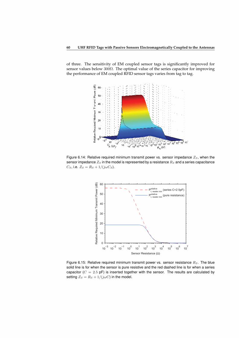
60 UHF RFID Tags with Passive Sensors Electromagnetically Coupled to the Antennas
of three. The sensitivity of EM coupled sensor tags is significantly improved forsensor values below 300Ω. The optimal value of the series capacitor for improvingthe performance of EM coupled RFID sensor tags varies from tag to tag.
Figure 6.14: Relative required minimum transmit power vs. sensor impedance ZS , when thesensor impedance ZS in the model is represented by a resistance RS and a series capacitanceCS , i.e. ZS = RS + 1/(jωCS).
10−3
10−2
10−1
100
101
102
103
104
105
106
107
0
10
20
30
40
50
60
Sensor Resistance (Ω)
Rela
tive R
equired M
inim
um
Tra
nsm
it P
ow
er
(dB
)
Prelative
t, reader min (series C=2.5pF)
Prelative
t, reader min (pure resistance)
Figure 6.15: Relative required minimum transmit power vs. sensor resistance RS . The bluesolid line is for when the sensor is pure resistive and the red dashed line is for when a seriescapacitor (C = 2.5 pF) is inserted together with the sensor. The results are calculated bysetting ZS = RS + 1/(jωC) in the model.
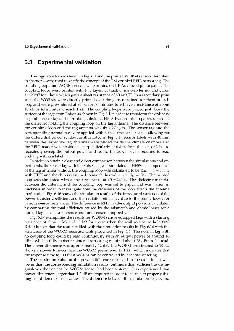
6.3 Experimental validation 61
6.3 Experimental validation
The tags from Rafsec shown in Fig. 6.1 and the printed WORM sensors describedin chapter 4 were used to verify the concept of the EM coupled RFID sensor tag. Thecoupling loops and WORM sensors were printed on HP Advanced photo paper. Thecoupling loops were printed with two layers of track of nano-sivler ink and curedat 120 C for 1 hour which gave a sheet resistance of 60 mΩ/. In a secondary printstep, the WORMs were directly printed over the gaps remained for them in eachloop and were pre-sintered at 90 C for 30 minutes to achieve a resistance of about10 kΩ or 40 minutes to reach 1 kΩ. The coupling loops were placed just above thesurface of the tags from Rafsec as shown in Fig. 6.1 in order to transform the ordinarytags into sensor tags. The printing substrate, HP Advanced photo paper, served asthe dielectric holding the coupling loop on the tag antenna. The distance betweenthe coupling loop and the tag antenna was thus 270 µm. The sensor tag and thecorresponding normal tag were applied within the same sensor label, allowing forthe differential power readout as illustrated in Fig. 2.1. Sensor labels with 40 mmbetween the respective tag antennas were placed inside the climate chamber andthe RFID reader was positioned perpendicularly at 0.8 m from the sensor label torepeatedly sweep the output power and record the power levels required to readeach tag within a label.
In order to obtain a clear and direct comparison between the simulations and ex-periments, the sensor tag with the Rafsec tag was simulated in HFSS. The impedanceof the tag antenna without the coupling loop was calculated to be ZA0 = 4 + j60 Ωwith HFSS and the chip is assumed to match this value, i.e. ZC = Z∗
A0. The printedloop was simulated with a sheet resistance of 60 mΩ/sq. The dielectric materialbetween the antenna and the coupling loop was set to paper and was varied inthickness in order to investigate how the closeness of the loop affects the antennamodulation. Fig. 6.16 shows the simulation results of the introduced variation of thepower transfer coefficient and the radiation efficiency due to the ohmic losses forvarious sensor resistances. The difference in RFID reader output power is calculatedby comparing the total efficiency caused by the mismatch and ohmic losses for anormal tag used as a reference and for a sensor equipped tag.
Fig. 6.17 exemplifies the results for WORM sensor equipped tags with a startingresistance of about 1 kΩ and 10 kΩ for a case when the wall was set to hold 80%RH. It is seen that the results tallied with the simulation results in Fig. 6.16 with theassistance of the WORM measurements presented in Fig. 4.4. The normal tag withno coupling loop could be read continuously with an output power of around 16dBm, while a fully moisture sintered sensor tag required about 28 dBm to be read.The power difference was approximately 12 dB. The WORM pre-sintered to 10 kΩshows a slower turn-on than the WORM presintered to 1 kΩ, which indicates thatthe response time to RH for a WORM can be controlled by heat pre-sintering.
The maximum value of the power difference retrieved in the experiment waslower than the corresponding simulation results, but more than sufficient to distin-guish whether or not the WORM sensor had been sintered. It is experienced thatpower differences larger than 1-2 dB are required in order to be able to properly dis-tinguish different sensor values. The difference between the simulation results and
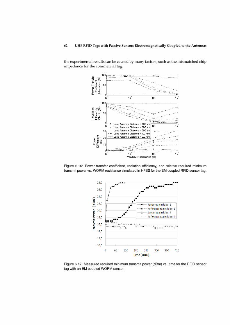
62 UHF RFID Tags with Passive Sensors Electromagnetically Coupled to the Antennas
the experimental results can be caused by many factors, such as the mismatched chipimpedance for the commercial tag.
Figure 6.16: Power transfer coefficient, radiation efficiency, and relative required minimumtransmit power vs. WORM resistance simulated in HFSS for the EM coupled RFID sensor tag.
Figure 6.17: Measured required minimum transmit power (dBm) vs. time for the RFID sensortag with an EM coupled WORM sensor.

6.4 Discussion 63
6.4 Discussion
A concept of electromagnetically coupled RFID sensor tags was presented in thischapter where electromagnetic coupling is used to modulate the tag antenna proper-ties. The EM coupling mechanism has been analyzed by showing how the antennaimpedance and radiation efficiency change with sensor impedance. Two equivalentcircuit models were respectively proposed for the EM coupled sensor tags with twotypes of antenna and the models were well verified by full-wave simulations. Theproposed models can thus be used to analyze the performance of the EM coupledsensor tags through circuit-level calculations rather that tedious full-wave simula-tions. The concept was also proved experimentally by applying the printed WORMsensor to be EM coupled to a commercial RFID tag.

64

Chapter 7
Investigation on the effect ofthe edge roughness on theantenna
The last decade’s rapid expansion of RFID-technology has constituted a drivingforce for low-cost high-speed antenna manufacturing methods. High speed manu-facturing processes are commonly associated with high mechanical tolerances. ForRFID antennas, mechanical manufacturing tolerances imply uncertainties in the an-tennas’ outer dimensions as well as in the surface- and edge-roughness of the an-tennas’ geometry. Printed antennas commonly receive a significantly higher surfaceroughness as compared to their etched counterparts. Screen-printed antennas, forexample, suffer from two different length scales of surface roughness, one due to thenature of the conductive ink itself and one due to mesh traces. Surface roughness forscreen printed RFID antennas is further described in [59] where an increase of theAC resistance per unit length by approximately 10% is observed, and with an over-all resonant frequency shift of about 1%. The largest portion of tag antennas have,so far, been manufactured by the high-speed subtractive production processes, e.g.etching and milling process. Etched and milled antennas have less surface rough-ness, but they may have a higher degree of edge roughness, Fig. 7.1, for example,shows the appearance of rough patterns produced by milling metallic foils. Roughedges lead to uncertainties in antenna properties such as resonant frequency and in-put impedance. Unforeseen antenna behavior can affect the measurements of theantenna-based sensor tags since the sensor tags should be constructed on a tag witha matched antenna and chip. Thus the tag antennas should be designed to be elec-tromagnetically robust against edge roughness that might be introduced to the an-tennas during manufacture. The influence of the edge roughness is thus investigatedhere.
This chapter characterizes the performance degradation for UHF RFID tag an-tennas, which is caused by rough edges on the antennas with a smooth surface. Theinvestigation in this work follows a deterministic approach when applying distor-tions to antenna structures and was conducted by full-wave simulations.
7.1 Method
Surface roughness and edge roughness are commonly quantified as the root meansquare (RMS) of the geometrical deviations that cause the roughness. In this inves-
65
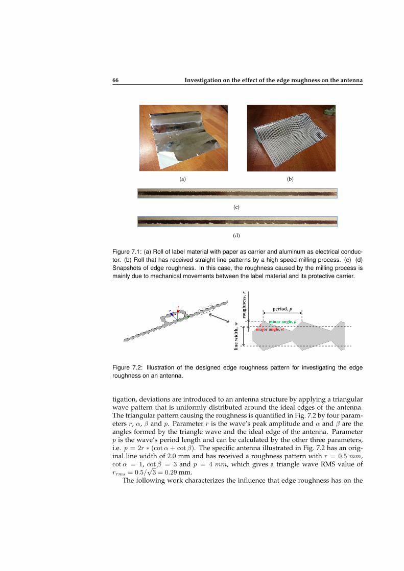
66 Investigation on the effect of the edge roughness on the antenna
(a) (b)
(c)
(d)
Figure 7.1: (a) Roll of label material with paper as carrier and aluminum as electrical conduc-tor. (b) Roll that has received straight line patterns by a high speed milling process. (c) (d)Snapshots of edge roughness. In this case, the roughness caused by the milling process ismainly due to mechanical movements between the label material and its protective carrier.
Figure 7.2: Illustration of the designed edge roughness pattern for investigating the edgeroughness on an antenna.
tigation, deviations are introduced to an antenna structure by applying a triangularwave pattern that is uniformly distributed around the ideal edges of the antenna.The triangular pattern causing the roughness is quantified in Fig. 7.2 by four param-eters r, α, β and p. Parameter r is the wave’s peak amplitude and α and β are theangles formed by the triangle wave and the ideal edge of the antenna. Parameterp is the wave’s period length and can be calculated by the other three parameters,i.e. p = 2r ∗ (cotα + cotβ). The specific antenna illustrated in Fig. 7.2 has an orig-inal line width of 2.0 mm and has received a roughness pattern with r = 0.5 mm,cotα = 1, cotβ = 3 and p = 4 mm, which gives a triangle wave RMS value ofrrms = 0.5/
√3 = 0.29 mm.
The following work characterizes the influence that edge roughness has on the
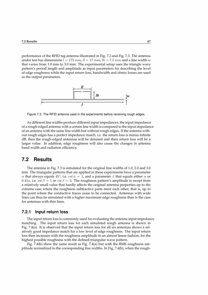
7.2 Results 67
performance of the RFID tag antenna illustrated in Fig. 7.2 and Fig. 7.3. The antennaunder test has dimensions l = 175 mm, ll = 17 mm, lh = 7.5 mm and a line width wthat varies from 1.0 mm to 3.0 mm. The experimental setup uses the triangle wavepattern’s period length and amplitude as input parameters for describing the levelof edge roughness while the input return loss, bandwidth and ohmic losses are usedas the output parameters.
Figure 7.3: The RFID antenna used in the experiments before receiving rough edges.
As different line widths produce different input impedances, the input impedanceof a rough-edged antenna with a certain line width is compared to the input impedanceof an antenna with the same line width but without rough edges. If the antenna with-out rough edges has a perfect impedance match, i.e. the return loss is minus infinitedB, then the rough-edged antennas will be detuned and their return loss will be alarger value. In addition, edge roughness will also cause the changes in antennaband width and radiation efficiency.
7.2 Results
The antenna in Fig. 7.3 is simulated for the original line widths of 1.0, 2.0 and 3.0mm. The triangular patterns that are applied in these experiments have a parameterα that always equals 45, i.e. cot α = 1, and a parameter β that equals either α or0.41α, i.e. cot β = 1 or cot β = 3. The roughness pattern’s amplitude is swept froma relatively small value that hardly affects the original antenna properties up to theextreme case where the roughness subtractive parts meet each other, that is, up tothe point where the conductive traces cease to be connected. Antennas with widelines can thus be simulated with a higher maximum edge roughness than is the casefor antennas with thin lines.
7.2.1 Input return loss
The input return loss is commonly used for evaluating the antenna input impedancematching. The input return loss for each simulated rough antenna is shown inFig. 7.4(a). It is observed that the input return loss for all six antennas shows a rel-atively good impedance match for a low level of edge roughness. The input returnloss then increases with the roughness amplitude in an almost linear fashion, for thehighest possible roughness with the defined triangular wave pattern.
Fig. 7.4(b) show the same result as Fig. 7.4(a) but with the RMS roughness am-plitude normalized to the corresponding line widths. In Fig. 7.4(b), when the rough-
68 Investigation on the effect of the edge roughness on the antenna
ness patterns have a certain triangle shape, i.e. have a fixed α and β, almost identicalchanges in input return loss are observed for the different antenna line widths. Forthe specific antenna structure used in this work, it is thus concluded that the levelof performance degradation due to edge roughness, in terms of input return loss, isrelated to the structure’s line width and not only related to the level of roughnessamplitude.
When the roughness patterns have different triangle shapes, i.e. have different αand β, the input return loss is less for the rough antennas with a larger wave periodp. Therefore, the level of performance degradation due to edge roughness is alsorelated to the wave period of the roughness pattern.
The exception occurs when the wave period of the roughness pattern is largerthan the height of the antenna loop, since the mean line-width of the loop will be-come larger and the inner area of the loop will become smaller.
0 0.2 0.4 0.6 0.8 1−35
−30
−25
−20
−15
−10
−5
0
Edge Roughness Amplitude (RMS) [mm]
S11 [
dB
]
w=1mm,cotα=1,cotβ=1
w=2mm,cotα=1,cotβ=1
w=3mm,cotα=1,cotβ=1
w=1mm,cotα=1,cotβ=3
w=2mm,cotα=1,cotβ=3
w=3mm,cotα=1,cotβ=3
(a)
0 0.1 0.2 0.3 0.4 0.5−35
−30
−25
−20
−15
−10
−5
0
Edge Roughness Amplitude (RMS) [mm]
Normalized to Antenna Line Width
S11 [
dB
]
w=1mm,cotα=1,cotβ=1
w=2mm,cotα=1,cotβ=1
w=3mm,cotα=1,cotβ=1
w=1mm,cotα=1,cotβ=3
w=2mm,cotα=1,cotβ=3
w=3mm,cotα=1,cotβ=3
(b)
Figure 7.4: Input return loss for different levels of edge roughness, at 868 MHz.
7.2 Results 69
7.2.2 Bandwidth
The previous subsection considered the deviations of the impedance for a rough-edged antenna from that of a smooth-edged antenna with the same line width ata single frequency. This subsection evaluates the impedance deviations at variousfrequencies from the impedance at 868 MHz for the individual antenna, in termsof bandwidth. That is, the bandwidth of an antenna with a specific line widthand a specific degree of edge roughness is calculated with the base in its own in-put impedance at 868 MHz and is not based upon comparisons with the smooth-edged original antenna. The bandwidth was calculated with a critical condition ofVSWR≤ 1.5 (VSWR: voltage standing wave ratio). It was observed that the band-width decreases with increased edge roughness for the specific antenna under test.This is shown in Fig. 7.5 where the bandwidth decreases from about 60 MHz to about40 MHz for each simulated antenna line width.
0.8 0.85 0.9 0.95 11
1.05
1.1
1.15
1.2
1.25
1.3
1.35
1.4
1.45
1.5
f (MHz)
VS
WR
No Edge Roughness
0.14mm RMS Roughness
0.29mm RMS Roughness
0.43mm RMS Roughness
0.56mm RMS Roughness
(a)
0 0.1 0.2 0.3 0.4 0.50
10
20
30
40
50
60
70
80
90
100
Edge Roughness Amplitude (RMS) [mm]
Normalized to Antenna Line Width
Bandw
idth
[M
Hz]
w=1mm
w=2mm
w=3mm
(b)
Figure 7.5: (a) VSWR for the antennas with different levels of edge roughness, when they havea line width of 2 mm and a triangular edge roughness pattern with parameters of α = β = 45.(b) Bandwidth decreases with increased edge roughness, when the triangular edge roughnesspattern has parameters of α = β = 45.
70 Investigation on the effect of the edge roughness on the antenna
7.2.3 Ohmic losses
A great deal of previous work on RFID tag antennas has focused on printing theantennas with electrically conductive ink, with a conductivity that is significantlylower than the antennas that are etched or milled from solid metal. It is there-fore of interest to investigate what effect a hypothetical printing process that createstraces with finite conductivity and rough edges would have on an RFID tag antenna.The results of simulating antennas with a sheet resistance of 50 mΩ/ are shown inFig. 7.6 where it is seen that ohmic losses increase with the roughness amplitude in alinear way and the effect is almost identical for different line widths if the roughnessamplitudes are normalized to the line widths. The effect of the edge roughness onthe ohmic losses is relatively mild compared to that on input return loss.
0 0.1 0.2 0.3 0.4 0.50
10
20
30
40
50
60
70
80
90
100
Edge Roughness Amplitude (RMS) [mm]
Normalized to Antenna Line Width
Ohm
ic R
adia
tion E
ffic
iency [
%]
w=1mm, 50 mΩ/sq
w=2mm, 50 mΩ/sq
w=3mm, 50 mΩ/sq
Figure 7.6: Radiation efficiency due to ohmic losses for the antennas with different levelsof edge roughness, when they have a triangular edge roughness pattern with parameters ofα = β = 45.
7.3 Discussion
For an RFID tag antenna, the edge roughness is relatively small and will not reachthe extreme case investigated, however, it can be concluded that an antenna with awider line width is more robust and can stand a higher degree of edge roughness.Antennas that are at risk of receiving a high degree of edge roughness should bedesigned to be electromagnetically robust against this kind of manufacturing issue.This initial investigation on the subject utilized relatively simple roughness models.More advanced statistical models such as those presented in [60] could indeed beutilized in order to characterize the effects of random edge roughness. The resultsof such an evaluation could advantageously constitute the basis for creating designguidelines for antennas that are robust against edge roughness.

Chapter 8
Summary of publications8.1 Paper I
This paper presents a concept of a UHF RFID humidity sensory tag which uti-lizes a moisture absorbing layer to provide humidity sensor functionality to an RFIDtag antenna and where an additional normal tag is used as a reference in order toallow differential readout of sensing information. This concept was previously pro-posed and demonstrated in [10] by using ordinary commercially available dipole-based RFID tag antennas. However, measurements of such one-layer antennas canencounter problems when they are placed on a background material that has a highpermittivity. The microstrip antennas are known as having a low influence frombackground materials. Therefore, this paper presents how microstrip antennas couldpossibly be used for such a humidity sensory tag in order to shield it from the back-ground materials. The design of the microstrip antenna is presented and the per-formance of the sensor tag is characterized both by applying water drops and byplacing the pair of antenna in a humid environment.
8.2 Paper II
This paper presents how an inkjet-printed structure can be a WORM memoryby heat sintering. This work is a primary study of the heat sintering effect of theprinted WORM structure and it shows that the printed structure will lower its re-sistance under high temperature and maintain its lowest achieved resistance value,making it a 1-bit resistive WORM memory. This paper also proposes a potentialpossibility to make the WORM memory serve as a temperature sensor. To sense thetemperature, the WORM sensor is directly integrated into an RFID tag antenna tomodulate the antenna’s performance. The characterization of the temperature sens-ing tag is shown by measuring the changes in the maximum reading distance andthe minimum transmit power required to power-up the tag.
8.3 Paper III
This paper presents the humidity sintering effect of the printed WORM memoryand how it can serve as a humidity sensor to indicate whether it has been exposedto a certain degree of humidity. The printed WORM memory permanently lowersits resistance after exposure to humidity or water. The WORM sensor is designed tobe directly embedded into the tag antenna and the change of the sensor resistance is
71

72 Summary of publications
used to modulate the properties of a UHF RFID tag antenna by changing the antennainput impedance and also by introducing or removing ohmic losses in the antennastructure. The final result is reflected in the change of the minimum transmit powerrequired to power-up the RFID tag. The modulation of the sensor resistance on theantenna electrical properties is characterized by simulations. Different geometriccombinations of sensor and antenna structures are investigated. Typical applicationsof such a humidity sensor tag are also discussed in the paper. The sensor setupcan serve to detect wetness or humidity levels in hidden locations such as withinconstruction structures and also provide information as to whether a package sentover a supply chain has exceeded a certain level of humidity during its route.
8.4 Paper IV
This paper presents another method for integrating the resistive sensor compo-nents into RFID tag antennas to construct antenna-based sensor tags. The resistivesensors are integrated into the tag antenna by means of electromagnetic coupling. Acoupling loop with an embedded resistive sensor is horizontally placed just abovethe surface of an ordinary UHF RFID tag and the sensor resistance is electromag-netically coupled to the tag antenna in order to modulate the properties of the tagantenna. The concept is experimentally verified by attaching a printed loop with anembedded WORM memory onto a commercial tag. The proposed concept showsthat commercial RFID tags can be used as sensor tags by simply adding an electro-magnetically coupled sensor as a sticker or by similar means, without the need forohmic contacts between the sensor and the original RFID tag.
8.5 Paper V
This paper proposes an analytical model for an electromagnetically coupled UHFRFID sensor tag which has a shunt/series inductors matched dipole antenna. Theantenna together with the coupling loop are represented as an equivalent circuit andthe analysis of the sensor tag becomes a circuit-level calculation after extracting pa-rameters from full-wave simulations for, respectively, the separated dipole antennaand coupling loop. The results calculated from the equivalent circuit model are com-pared with the results from full-wave simulations and show good agreement. Thepresented model can thus be an excellent alternative to full-wave simulation soft-ware when analyzing and predicting the behavior of electromagnetically coupledsensor tags, in order to save time and computational resource. Based on the analysiswith the presented model, the methods for optimizing the sensory performance ofthis kind of RFID sensor tags are also presented in this paper.
8.6 Paper VI
This paper continues the study on the electromagnetically coupled UHF RFIDsensor tags and discusses the key factors affecting the performance of the EM cou-

8.7 Paper VII 73
pled RFID sensor tags. The distance between the coupling loop and the antenna hasan impact on the coupling coefficient and it will obviously affect the performance ofthe EM coupled sensor tags. In addition, the choice of the tag antenna structures hasless influence and the choice of tag chip will have a more significant influence. In acomplementary manner, this paper also proposes an equivalent circuit model for theEM coupled sensor tags with another type of antenna structure, i.e. a dipole withinductively coupled loop for matching. The model is verified by comparison withthe full-wave simulation results. The inductively coupled dipole antenna is anotherbasic antenna structure for UHF RFID tags, in addition to that of the shunt/seriesinductors matched dipole antenna. The majority of the UHF RFID tag antennas arevariants of these two basic antenna structures. The analytical models for these twoantenna structures can be derived to be suitable for other tag antennas by varying theantenna equivalent circuit parameters or by slightly adjusting the equivalent circuitmodel.
8.7 Paper VII
This paper summarizes the two basic ideas with regards to the integration of thepassive sensor components into UHF RFID tag antennas, i.e. the method of directinsertion integration and the method of electromagnetic coupling integration. Theideas are demonstrated, in this paper, by implementing on/off tilt sensors and pres-sure sensors.
8.8 Paper VIII
This paper shows two printed memory designs within PriMeBits project, a FRAMmemory and a WORM memory, and demonstrates their possible applications insmart packaging and storage on paper.
8.9 Paper IX
Thin inkjet-printed tracks of silver nano-particles have previously been observedto show a non-reversible decrease in resistance when exposed to a high degree of rel-ative humidity and thus providing sensor functionality with a memory effect. Thisarticle provides a more in-depth explanation regarding the observed humidity sen-sor effect that originates from inkjet-printed silver nano-particle sensors on papersubstrate. It is shown that the geometry of the sensor has a large effect on the sen-sor’s initial resistance, and therefore also on the sensor’s resistive dynamic range.The importance of the sensor geometry is believed to be due to the amount of inksolvent that interacts with the coating of the paper substrate, which in turn enablesdiffusion of salts from the paper coating into the ink.

74 Summary of publications
8.10 Paper X
This work investigates the impact that the edge roughness of an antenna struc-ture has on UHF RFID tag’s communication capabilities. Edge roughness is a com-monly existing phenomenon for the antennas manufactured by high speed manufac-turing processes. The work characterizes the negative influence that edge roughnessof different levels has on standard RFID dipoles. Results show that, as expected,the performance degradation for an RFID tag antenna increases with increased edgeroughness. The results also show that the changes in antenna properties due to edgeroughness are almost identical to those for the investigated antenna line widthswhen the roughness level is normalized to its specific antenna line width. The re-sults indicate that an antenna with a wider line width is more robust and can stand ahigher degree of edge roughness. This work uses a relatively simple pattern to sim-ulate the edge roughness and it is the first step to conducting such an investigationin relation to the impact of edge roughness on the RFID tag antenna, however, theresults of this investigation could advantageously constitute the basis for creatingdesign guidelines for antennas that are robust against edge roughness.
8.11 Author’s contributions
The contribution of the author of this thesis to each paper has been summarizedin Table 8.11.

8.11 Author’s contributions 75
Table 8.1: Author’s contribution (M=Main author, C=Co-author)
Paper JG1 JS2 HN3 HA4 AA5 MG6 AM7 BN8 TU9 PJ10 CL,SF11 O12
IC M C
JG: Measurements, discussion and writing (40%)
IIM C C
JG: Main writer and measurements (95%)
IIIM C C C
JG: Main writer, simulations and measurements (80%)
IVM C C
JG: Main writer and measurements (80%)
VM C C
JG: Main writer, modeling and simulations (95%)
VIM C C
JG: Main writer, modeling and simulations (98%)
VIIC M C C C C C
JG: Discussion, measurements and writing (30%)
VIIIC C C C M C C C
JG: Measurements on the single-bit humidity sensors (8%)
IXC C C M C C C
JG: Discussion and measurements (20%)
XM C C
JG: Main writer and simulations (60%)1 Jinlan Gao 11 Cecilia Lidenmark, Sven Forsberg2 Johan Siden 12 Tomi Mattila, Jaakko Leppaniemi,3 Hans-Erik Nilsson 12 Mika Suhonen, Terho Kololuoma,4 Henrik Andersson Andreas Schaller, Alexandru Rusu,5 Ari Alastalo Suat Ayoz, Igor Stolichnov,6 Mikael Gulliksson Simo Siitonen, Tobias Lehnert,7 Anatoliy Manuilskiy Jens Adam, Michael Veith,8 Bjorn Neubauer Alexey Merkulov, Yvonne Damaschek,9 Tomas Unander Jurgen Steiger, Markus Cederberg10 Peter Jonsson Miroslav Konecny

76

Chapter 9
Thesis SummaryThis thesis has presented three approaches in relation to adding sensor function-
ality to standard passive UHF RFID tags. All three approaches utilize the sensor tomodulate the tag antenna properties and readout the sensor information by evaluat-ing the performance of the tag antenna. The presented antenna-based RFID sensortags target low-cost applications, which do not require high-precision sensing. Thepresented RFID sensor tag designs are potentially suitable for many kinds of sensorsand the work in this thesis mainly focuses on characterizing the humidity sensing.A novel low-cost printed humidity sensor with memory functionality was presentedand used for experimentally validating the proposed approaches of integration ofthe sensors into passive UHF RFID tags.
Chapter 3 presented how a moisture absorbing layer could provide humiditysensor functionality to UHF RFID tag antennas for in-situ humidity surveillance andhow a microstrip antenna could be used to shield the influence of the backgroundmaterials on such a humidity sensor tag. Chapter 4 introduced an ultra-low-costhumidity sensor printed by conductive ink, which works as a WORM memory andcan be used to detect the event of excessive humidity. Both the design and the char-acterizations of the WORM sensor were presented. Since the WORM sensor canrecord the event and its value can be read out at a later stage, the WORM bridgesthe time gap and is thus suitable for watchdog applications. Chapter 5 and chapter6 illustrated two methods to integrate a small resistive sensor component, such asa WORM, into a tag antenna. The integration of the sensor by means of galvaniccontact can be achieved in two opposite ways. In this regard, the integration of thesensor by means of electromagnetic coupling is a non-contact solution. It is an easiermeans of assembling the sensors and is particularly suitable for the one-time-usageWORM sensors since the RFID tags can be reused by simply supplying new couplingloops and sensors. Both the theoretical analysis and the experimental validation ofthe proposed RFID sensor tags have been presented in this thesis.
The measurable variables and the measurement setup for the antenna-based RFIDsensor tags have also been discussed in chapter 2.
To manufacture low-cost RFID tags, a few high-speed manufacturing processesexist for fabricating the antennas. Both an additive process and a subtractive processwill cause a certain degree of roughness to the antennas. Rough edges lead to un-certainties in antenna properties such as resonant frequency and input impedance.Unforeseen antenna behavior can affect the measurements of the antenna-based sen-sor tags since the sensor tags should be constructed on a tag with a matched antennaand chip. Thus the tag antennas should be designed to be electromagnetically robustagainst edge roughness that might be introduced to the antennas during manufac-
77

78 Thesis Summary
ture. Chapter 7 investigated the effect of the edge roughness on the performance ofthe antenna by analyzing the detuning of the antenna’s electrical properties causedby various degrees of edge roughness. This investigation utilizes a relatively sim-ple structural model to simulate the edge roughness caused by the manufacturingprocess and shows a preliminary result, however, this preliminary result could ad-vantageously constitute the basis for creating design guidelines for antennas that arerobust against edge roughness.

References[1] V. Subramanian, J. Frechet, P. Chang, D. Huang, J. Lee, S. Molesa, A. Mur-
phy, D. Redinger, and S. Volkman, “Progress toward development of all-printedRFID tags: Materials, processes, and devices,” Proceedings of the IEEE, vol. 93,no. 7, pp. 1330 –1338, July 2005.
[2] V. Subramanian, J. B. Chang, A. d. l. F. Vornbrock, D. C. Huang, L. Jagannathan,F. Liao, B. Mattis, S. Molesa, D. R. Redinger, D. Soltman, S. K. Volkman, andQ. Zhang, “Printed electronics for low-cost electronic systems: Technology sta-tus and application development,” in 38th European Solid-State Device ResearchConf., ESSDERC 2008, pp. 17 –24.
[3] A. Rida, L. Yang, R. Vyas, and M. Tentzeris, “Conductive inkjet-printed an-tennas on flexible low-cost paper-based substrates for RFID and WSN appli-cations,” IEEE Antennas and Propag. Mag., vol. 51, no. 3, pp. 13 –23, Jun. 2009.
[4] S. Leung and D. Lam, “Geometric and compaction dependence of printedpolymer-based RFID tag antenna performance,” IEEE Trans. Electron. Packag.Manuf., vol. 31, no. 2, pp. 120 –125, Apr. 2008.
[5] A. Sample, D. Yeager, P. Powledge, A. Mamishev, and J. Smith, “Design of anrfid-based battery-free programmable sensing platform,” IEEE Trans. Instrum.Meas., vol. 57, no. 11, pp. 2608 –2615, Nov. 2008.
[6] D. Yeager, P. Powledge, R. Prasad, D. Wetherall, and J. Smith, “Wirelessly-charged uhf tags for sensor data collection,” in IEEE Int. Conf. RFID, Apr. 2008,pp. 320 –327.
[7] M. Tentzeris, “Novel paper-based inkjet-printed antennas and wireless sensormodules,” in IEEE Int. Conf. Microwaves, Communications, Antennas and Elec-tronic Systems, COMCAS 2008., May, pp. 1 –8.
[8] A. Vaz, A. Ubarretxena, I. Zalbide, D. Pardo, H. Solar, A. Garcia-Alonso, andR. Berenguer, “Full passive uhf tag with a temperature sensor suitable for hu-man body temperature monitoring,” IEEE Trans. Circuits Systems II: ExpressBriefs, vol. 57, no. 2, pp. 95 –99, Feb. 2010.
[9] K. Chang, Y.-H. Kim, Y.-J. Kim, and Y. J. Yoon, “Patch antenna using synthesizedpolyimide for rfid sensing,” in The 9th European Conf. Wireless Technology, Sept.2006, pp. 83 –86.
[10] J. Siden, X. Zeng, T. Unander, A. Koptyug, and H.-E. Nilsson, “Remote moisturesensing utilizing ordinary rfid tags,” in IEEE Sensors 2007, Oct. 2007, pp. 308 –311.
79

80 REFERENCES
[11] C. Occhiuzzi, A. Rida, G. Marrocco, and M. Tentzeris, “Rfid passive gas sensorintegrating carbon nanotubes,” IEEE Trans. Microw. Theory Tech., vol. 59, no. 10,pp. 2674 –2684, Oct. 2011.
[12] S. Caizzone, C. Occhiuzzi, and G. Marrocco, “Multi-chip rfid antenna integrat-ing shape-memory alloys for detection of thermal thresholds,” IEEE Trans. An-tennas Propag., vol. 59, no. 7, pp. 2488 –2494, Jul. 2011.
[13] R. Bhattacharyya, C. Floerkemeier, and S. Sarma, “Towards tag antenna basedsensing - an rfid displacement sensor,” in IEEE Int. Conf. RFID, 2009, pp. 95–102.
[14] J. Virtanen, L. Ukkonen, T. Bjorninen, L. Sydanheimo, and A. Elsherbeni, “Tem-perature sensor tag for passive uhf rfid systems,” in IEEE Sensors ApplicationsSymp. (SAS), Feb. 2011, pp. 312 –317.
[15] R. Bhattacharyya, C. Floerkemeier, and S. Sarma, “Rfid tag antenna based tem-perature sensing,” in IEEE Int. Conf. RFID, 2010, pp. 8 –15.
[16] J. Virtanen, L. Ukkonen, T. Bjorninen, A. Elsherbeni, and L. Syda andnheimo,“Inkjet-printed humidity sensor for passive uhf rfid systems,” IEEE Trans. In-strum. Meas., vol. 60, no. 8, pp. 2768 –2777, Aug. 2011.
[17] Melexis chip, MLX90129, 13.56 MHz RFID Sen-sor transponder IC datasheet. [Online]. Available:http://www.melexis.com/Assets/MLX90129 DataSheet 5193.aspx
[18] IDS sensory tag chip, SL900A, EPC Class 3 chip with sensor for automaticdata logging - summary data sheet. [Online]. Available: http://ids-microchip.com/upload/4025878-SL900A-SD.pdf
[19] A.-L. Pasanen, J.-P. Kasanen, S. Rautiala, M. Ikaheimo, J. Rantamaki,H. Kaariainen, and P. Kalliokoski, “Fungal growth and survival in building ma-terials under fluctuating moisture and temperature conditions,” InternationalBiodeterioration & Biodegradation, vol. 46, no. 2, pp. 117 – 127, 2000.
[20] SCA Cool Logistics International Group. [Online]. Available: http://www.sca-cool-logistics.com
[21] A. Pacquit, J. Frisby, D. Diamond, K. T. Lau, A. Farrell, B. Quilty, and D. Dia-mond, “Development of a smart packaging for the monitoring of fish spoilage,”Food Chemistry, vol. 102, no. 2, pp. 466 – 470, 2007.
[22] N. P. Mahalik and A. N. Nambiar, “Trends in food packaging and manufactur-ing systems and technology,” Trends in Food Science & Technology, vol. 21, no. 3,pp. 117 – 128, March 2010.
[23] E. L. Tan, W. N. Ng, R. Shao, B. D. Pereles, and K. G. Ong, “A wireless, passivesensor for quantifying packaged food quality,” Sensors, vol. 7, no. 9, pp. 1747–1756, Sep. 2007.

REFERENCES 81
[24] D. M. Dobkin, The RF in RFID: Passive UHF RFID in Practice. Newton, MA,USA: Newnes, 2007.
[25] T. S. Rapppaport, Wireless Communications-Principles and Practice, 2nd ed. Pren-tice Hall, Pearson Education (US), 2001.
[26] A. Lazaro, D. Girbau, and D. Salinas, “Radio link budgets for UHF RFID onmultipath environments,” IEEE Trans. Antennas Propag., vol. 57, no. 4, pp. 1241–1251, Apr. 2009.
[27] J. Griffin, G. Durgin, A. Haldi, and B. Kippelen, “Rf tag antenna performanceon various materials using radio link budgets,” IEEE Antennas Wireless Propag.Lett., vol. 5, no. 1, pp. 247–250, 2006.
[28] D. Dobkin and S. Weigand, “Environmental effects on rfid tag antennas,” inIEEE MTT-S Int. Microw. Symp., 2005, pp. 135–138.
[29] J. Siden and H.-E. Nilsson, “Adaption to background material for printed RFIDantennas,” in Proc. Antenn-06, Sweden, 2006.
[30] T. Hauschild and F. Menke, “Moisture measurement in masonry walls using anon-invasive reflectometer,” Electronics Letters, vol. 34, no. 25, pp. 2413–2414,1998.
[31] T. Uesaka, Dimensional stability and environmental effects of paper properties,2nd ed. New York, USA: Marcel Dekker, 2002.
[32] L. Reindl, C. C. W. Ruppel, A. Kirmayr, N. Stockhausen, M. Hilhorst, and J. Bal-endonck, “Radio-requestable passive saw water-content sensor,” IEEE Trans.Microw. Theory Tech., vol. 49, no. 4, pp. 803–808, 2001.
[33] H. Wang, X. Qiao, J. Chen, X. Wang, and S. Ding, “Mechanisms of PVP in thepreparation of silver nanoparticles,” Materials Chemistry and Physics, vol. 94, no.23, pp. 449 – 453, 2005.
[34] L. Mo, D. Liu, X. Zhou, and L. Li, “Preparation and conductive mechanism ofthe ink-jet printed nanosilver films for flexible display,” in 2nd Int. Congress onImage and Signal Processing, CISP ’09., 2009, pp. 1–5.
[35] J. R. Greer and R. A. Street, “Thermal cure effects on electrical performance ofnanoparticle silver inks,” Acta Materialia, vol. 55, no. 18, pp. 6345 – 6349, 2007.
[36] B. J. Perelaer, A. W. M. de Laat, C. E. Hendriks, and U. S. Schubert, “Inkjet-printed silver tracks: low temperature curing and thermal stability investiga-tion,” J. Mater. Chem., vol. 18, pp. 3209–3215, 2008.
[37] M. L. Allen, M. Aronniemi, T. Mattila, A. Alastalo, K. Ojanpera, M. Suhonen,and H. Seppa, “Electrical sintering of nanoparticle structures,” Nanotechnology,vol. 19, no. 17, p. 175201, 2008.

82 REFERENCES
[38] A. T. Alastalo, H. Seppa, J. H. Leppaniemi, M. J. Aronniemi, M. L. Allen, andT. Mattila, “Modelling of nanoparticle sintering under electrical boundary con-ditions,” J. Phys. D: Appl. Phys., vol. 43, no. 48, p. 485501, 2010.
[39] J. Leppaniemi, M. Aronniemi, T. Mattila, A. Alastalo, M. Allen, and H. Seppa,“Printed WORM memory on a flexible substrate based on rapid electrical sin-tering of nanoparticles,” IEEE Trans. Electron Devices, vol. 58, no. 1, pp. 151 –159,Jan. 2011.
[40] J. Kang, J. Ryu, H. Kim, and H. Hahn, “Sintering of inkjet-printed silvernanoparticles at room temperature using intense pulsed light,” Journal of Elec-tronic Materials, vol. 40, no. 11, pp. 2268–2277, 2011.
[41] T. Kumpulainen, J. Pekkanen, J. Valkama, J. Laakso, R. Tuokko, andM. Mantysalo, “Low temperature nanoparticle sintering with continuous waveand pulse lasers,” Optics & Laser Technology, vol. 43, no. 3, pp. 570 – 576, 2011.
[42] J. Perelaer, B.-J. deGans, and U. Schubert, “Ink-jet printing and microwave sin-tering of conductive silver tracks,” Advanced Materials, vol. 18, no. 16, pp. 2101–2104, 2006.
[43] N. R. Bieri, J. Chung, S. E. Haferl, D. Poulikakos, and C. P. Grigoropoulos, “Mi-crostructuring by printing and laser curing of nanoparticle solutions,” AppliedPhysics Letters, vol. 82, no. 20, pp. 3529–3531, 2003.
[44] J. Chung, S. Ko, N. R. Bieri, C. Grigoropoulos, and D. Poulikakos, “Conduc-tor microstructures by laser curing of printed gold nanoparticle ink,” AppliedPhysics Letters, vol. 84, no. 5, pp. 801–803, 2004.
[45] A. Khan, N. Rasmussen, V. Marinov, and O. F. Swenson, “Laser sintering ofdirect write silver nano-ink conductors for microelectronic applications,” pp.687 910–687 910–11, 2008.
[46] S. H. Ko, H. Pan, C. P. Grigoropoulos, C. K. Luscombe, J. M. J. Frechet, andD. Poulikakos, “All-inkjet-printed flexible electronics fabrication on a polymersubstrate by low-temperature high-resolution selective laser sintering of metalnanoparticles,” Nanotechnology, vol. 18, no. 34, p. 345202, 2007.
[47] P. Peng, A. Hu, and Y. Zhou, “Laser sintering of silver nanoparticle thin films:microstructure and optical properties,” Applied Physics A, vol. 108, no. 3, pp.685–691, 2012.
[48] S. Magdassi, M. Grouchko, O. Berezin, and A. Kamyshny, “Triggering the sin-tering of silver nanoparticles at room temperature,” ACS Nano, vol. 4, no. 4, pp.1943–1948, 2010.
[49] M. Allen, J. Leppaniemi, M. Vilkman, A. Alastalo, and T. Mattila, “Substrate-facilitated nanoparticle sintering and component interconnection procedure,”Nanotechnology, vol. 21, no. 47, p. 475204, 2010.
REFERENCES 83
[50] W. Zapka, W. Voit, C. Loderer, and P. Lang, “Low temperature chemical post-treatment of inkjet printed nano-particle silver inks,” in Proc. 24th Int. Conf. Dig-ital Print. Technol./Digital Fabricat., 2008, p. 906911.
[51] D. Wakuda, C.-J. Kim, K.-S. Kim, and K. Suganuma, “Room temperature sinter-ing mechanism of ag nanoparticle paste,” in 2nd Electronics System-IntegrationTechnology Conference, ESTC 2008., 2008, pp. 909–914.
[52] Y. Tang, W. He, G. Zhou, S. Wang, X. Yang, Z. Tao, and J. Zhou, “A new ap-proach causing the patterns fabricated by silver nanoparticles to be conductivewithout sintering,” Nanotechnology, vol. 23, no. 35, p. 355304, 2012.
[53] M. Grouchko, A. Kamyshny, C. F. Mihailescu, D. F. Anghel, and S. Magdassi,“Conductive inks with a built-in mechanism that enables sintering at room tem-perature,” ACS Nano, vol. 5, no. 4, pp. 3354–3359, 2011.
[54] H. Andersson, A. Manuilskiy, T. Unander, C. Lidenmark, S. Forsberg, andH. Nilsson, “Inkjet printed silver nanoparticle humidity sensor with memoryeffect on paper,” IEEE Sensors J., vol. 12, no. 6, pp. 1901 –1905, Jun. 2012.
[55] J. Voutilainen, O. Valta, E. Tommila, and R. Sepponen, “Novel measurementmethod of humidity within construction structures,” helsinki University ofTechnology, Espoo, Series E: Electronic Publications E 2, pp. 1-12, 2002.
[56] L. Yang, A. Rida, R. Vyas, and M. Tentzeris, “RFID tag and RF structures on apaper substrate using inkjet-printing technology,” IEEE Trans. Microw. TheoryTech., vol. 55, no. 12, pp. 2894 –2901, Dec. 2007.
[57] T. C. Chau, B. A. Welt, and W. R. Eisentadt, “Analysis and characterization oftransponder antennae for radio frequency identification (rfid) systems,” Pack-aging Technology and Science, vol. 19, no. 1.
[58] Alien Higgs-4 IC Product Overview. [Online]. Avail-able: http://www.alientechnology.com/docs/products/Alien-Technology-Higgs-4-EPC-Class-1-Gen-2-RFID-Tag-IC.pdf
[59] D.-Y. Shin, Y. Lee, and C. H. Kim, “Performance characterization of screenprinted radio frequency identification antennas with silver nanopaste,” ThinSolid Films, vol. 517, no. 21, pp. 6112 – 6118, 2009.
[60] T. Olsson and A. Koptioug, “Statistical analysis of antenna robustness,” IEEETrans. Antennas Propag., vol. 53, no. 1, pp. 566–570, Jan. 2005.

84