Embed Size (px)
Citation preview

AN1445
Antenna design guide for MFRC52x, PN51x and PN53x Rev. 1.2 — 11 October 2010 144512
Application note PUBLIC
Document information Info Content Keywords NFC, MFRC522, MFRC523, PN511, PN512, PN531, PN532, Antenna
Design, RF Design, constant current design
Abstract This application notes provides guidance on antenna and RF design for NFC devices MFRC522, MFRC523, PN511, PN512, PN531, PN532

NXP Semiconductors AN1445 Antenna design guide for MFRC52x, PN51x and PN53x
AN1445_12 All information provided in this document is subject to legal disclaimers. © NXP B.V. 2010. All rights reserved.
Application note PUBLIC
Rev. 1.2 — 11 October 2010 144512
2 of 65
Contact information For additional information, please visit: http://www.nxp.com For sales office addresses, please send an email to: [email protected]
Revision history Rev Date Description 1.2 20101011 Update with MFRC522 and MFRC523 1.1 2008/02/22 Selection Guide and all topologies added 1.0 2007/10/31 Initial Release

NXP Semiconductors AN1445 Antenna design guide for MFRC52x, PN51x and PN53x
AN1445_12 All information provided in this document is subject to legal disclaimers. © NXP B.V. 2010. All rights reserved.
Application note PUBLIC
Rev. 1.2 — 11 October 2010 144512
3 of 65
1. Introduction
1.1 Purpose and Scope This application note is intended to give a practical guide to design and dimension antennas and RF parts for contactless reader as well as NFC devices. The application note will provide the required understanding to design application specific antennas and dimensioning RF parts to achieve the best performance for a communication according to the different communication schemes of the ICs.
The RF part covers the required matching circuit to match an application specific antenna coil to the output driver of the MFRC522/MFRC523/PN51x/PN53x as well as the receiving circuit in order to detect a received RF signal.
1.2 MFRC52x/PN51x/PN53x features The MFRC522/MFRC523/PN51x/PN53x devices are designed to communicate in three different operation modes:
1. Reader/Writer mode to communicate to an ISO/IEC14443A, MIFARE card up to 100 mm depending on the antenna size and tuning. (MFRC52x /PN51x/PN53x).
2. Reader/Writer mode to communicate to a ISO/IEC14443 B card up to 100 mm depending on the antenna size and tuning (MFRC523/PN51x/PN53x).
3. Reader/Writer mode to communicate to a FeliCa card up to 100 mm depending on the antenna size and tuning (PN51x, PN53x).
4. NFCIP-1 mode to communicate to another NFC devices up to 100 mm depending on the antenna sizes and tuning (PN51x, PN53x).
5. ISO/IEC14443A, MIFARE card or FeliCa card mode to communicate to ISO/IEC14443A, MIFARE or FeliCa reader up to 100 mm depending on the generated external field strength. (PN51x, PN53x)
The MFRC52x/PN51x/PN53x’s overall functionality can be separated into three functions: 6. Generate the RF field: The generated magnetic field has to be maximized within the
limits of the transmitter supply current and general emission limits. 7. Transmit data: The coded and modulated data signal has to be transmitted in a way,
that every card and MFRC52x /PN51x/PN53x device is able to receive it. The signal shape and timing according to relevant standards has to be considered.
8. Receive data: The response of a card or MFRC52x /PN51x/PN53x device has to be transferred to the receive input of the PN51x/PN53x considering various limits, e.g. maximum voltage and receiver sensitivity.
The operating distance for the MFRC52x/PN51x/PN53x depends on • the matching of the antenna, • the sensitivity of the receiving part, • the antenna size of the device, • the antenna size of the communication partner and • external parameters, such as metallic environment and noise.

NXP Semiconductors AN1445 Antenna design guide for MFRC52x, PN51x and PN53x
AN1445_12 All information provided in this document is subject to legal disclaimers. © NXP B.V. 2010. All rights reserved.
Application note PUBLIC
Rev. 1.2 — 11 October 2010 144512
4 of 65
Note: MFRC52x devises are Reader/Writer devises only. So these are not able to operate in target mode.
2. How to use this document The application note is intended to give a practical guide to choose the matching topology, to design antennas and calculate the matching components for the MFRC52x/PN51x/PN53x RF part. It gives a guideline starting with the recommended RF matching circuitry description as well as a dedicated description of the transmitter matching resistance and matching procedure in each chapter. The appendix of this document provides an introduction in the overall antenna design theory for the system.
Depending on the target applications, different design decisions can be made in order to optimize the antenna topology. The environmental constraints of a device/antenna are the influencing detuning parameters for the RX-path and have to be investigated. Conditions for a detuning are determined by the type of an application and housing, e.g. peer-to-peer mode, card mode, metal or composite plastic housing. These effects can cause large voltage drops at the RX-site and therefore may affect demodulation of the signal.
The user needs to follow the selection guide in chapter 3 to choose the appropriate antenna topology!
This application note is outlined as followed
1. Antenna Selection Guide
2. Antenna Topology I
3. Antenna Topology II
4. Adoptions of Antenna Topology I or II
5. Antenna Topology III
6. Appendix a. The appendix includes information describing the calculation of the inductance of an antenna coil and gives basic hints on symmetry and environmental influences. The calculation of the equivalent circuits and an overview of all relevant formulas are give as well as Tips and hints to check the antenna and RF part design.
Each Antenna Topology provides information about a. The RF part block diagram. It shows a recommended circuitry design with all
relevant components required to connect an antenna to the PN51x/PN53x. It also ensures the transmission of energy and data to the target device as well as the reception of a target device answer.
b. The TX matching resistance Rmatch is explained which is required to calculate the remaining components and to optimize PN51x/PN53x power consumption.

NXP Semiconductors AN1445 Antenna design guide for MFRC52x, PN51x and PN53x
AN1445_12 All information provided in this document is subject to legal disclaimers. © NXP B.V. 2010. All rights reserved.
Application note PUBLIC
Rev. 1.2 — 11 October 2010 144512
5 of 65
c. Formulas to calculate the EMC filter and the matching circuit d. Antenna tuning procedure e. Design and calculation of the receiving part f. Example calculations
Note: This application note does not replace the relevant datasheets referenced in chapter 9.
“Card” in this document means a contactless smart card according to the ISO/IEC14443A (or MIFARE) or a contactless card according to the FeliCa scheme. Design hints on how to place the components on a PCB are not included. Tuning and measurement of the antenna has always to be performed at the final mounting position to consider all parasitic effects, e.g. metal influence on quality factor, inductance and additional capacitance.
All topologies and design methods described in this document assume antenna and tuning components are not accessible to end user. Therefore no additional ESD protection methods are described. In case antenna wiring is accessible from device housing or after user removable parts are detached, additional ESD protection has to be evaluated. Methods described here are then no more generally valid. Increased RF output power and communication distance could be achieved by integrating the RF amplifier for NXP’s contactless Reader IC’s ([13]).

NXP Semiconductors AN1445 Antenna design guide for MFRC52x, PN51x and PN53x
AN1445_12 All information provided in this document is subject to legal disclaimers. © NXP B.V. 2010. All rights reserved.
Application note PUBLIC
Rev. 1.2 — 11 October 2010 144512
6 of 65
3. Selection Guide The following flow chart describes a selection guide for different antenna topologies. The user needs to start from the top rectangle going downwards. Due to different detuning effects on the antenna only one of the following topologies may apply to the type of reader integration.
Antenna Topology I Antenna Topology II Asymmetric antenna tuning according to chapter 6 Antenna Topology III
Verify detuning at RX-Path according to chapter 4.6
“Receiver Circuit Design”
MIFARE, Type-A/B, FeliCa,
Peer-to-Peer
If communication problems occur, that can not be resolved by adjusting register
settings or RX-path dimensioning, Antenna Topology II needs to be
applied.
This is the starting point of the selection guide. This means, all indicated protocols can be supported by the following antenna topologies.
Antenna Topology II resolves strong detuning effects on the matching circuit.
Antenna Topology III has the same physical constraints as the asymmetric tuning of the recent topologies. Antenna Topology III requires less matching components.
If Antenna Topology I and II cannot counteract communication errors in certain distances, the EMC filter and matching circuit has to be adjusted according to chapter 6
It is recommended to start with Antenna Topology I since this is the basis for
possible further adoptions.

NXP Semiconductors AN1445 Antenna design guide for MFRC52x, PN51x and PN53x
AN1445_12 All information provided in this document is subject to legal disclaimers. © NXP B.V. 2010. All rights reserved.
Application note PUBLIC
Rev. 1.2 — 11 October 2010 144512
7 of 65
4. Antenna Topology I The RF block diagram in Fig 1 shows a recommended circuitry design with all relevant components required to connect an antenna to the MFRC522/MFRC523/PN51x/PN53x. It also ensures the transmission of energy and data to the target device as well as the reception of a target device answer.
Fig 1. Block diagram of the complete RF part
Note: Fig 1 shows only the RF part and the related power supply (TVDD and TVSS). For a proper operation the analog and digital supplies and the host interface have to be connected too.
Note: Topology I is the preferred RF part topology for MFRC522 and MFRC523
Although some of theses blocks may contain only a few passive components, it is important to consider all these blocks and all their functionality to guarantee the proper working of the complete device.
The EMC filter reduces 13.56 MHz harmonics and performs an impedance transformation. The Matching Circuit acts as an impedance transformation block. The antenna coil itself generates the magnetic field. The receiving part provides the received signal to the MFRC522/MFRC523/PN51x/PN53x internal receiving stage. Basically this complete RF circuitry consists of at least 8 capacitors (max. voltage ~50V types), 2 inductors, 2 resistors (the part size determines the maximum power which the resistor can withstand) and the symmetrical antenna coil as shown in Fig 1.

NXP Semiconductors AN1445 Antenna design guide for MFRC52x, PN51x and PN53x
AN1445_12 All information provided in this document is subject to legal disclaimers. © NXP B.V. 2010. All rights reserved.
Application note PUBLIC
Rev. 1.2 — 11 October 2010 144512
8 of 65
4.1 Equivalent circuit The following subchapters describe the matching procedure. It starts with the determination of the antenna parameters and ends with a fine tuning of the antenna circuitry.
4.1.1 Determination of series equivalent circuit The antenna loop has to be connected to an impedance or network analyzer to measure the series equivalent components.
Note: The equivalent circuit (see Fig 2) must be determined under final environmental conditions especially if the antenna will be operated in metal environment or a ferrite will be used for shielding.
Antenna
Ra
La
Ca
Fig 2. Series equivalent circuit
Typical values:
La = 0.3...3 µH
Ca = 3...30 pF
Ra = 0.3...8 Ω
4.1.2 Calculation of antenna quality factor damping resistor RQ The quality factor of the antenna is calculated with
a
aa R
LQ ⋅=ω
If the calculated value of Qa is higher than the target value of 35, an external damping resistor RQ has to be inserted on each antenna side to reduce the Q-factor to a value of 35 (±10%).
The value of RQ (each side of the antenna) calculates as
−
⋅⋅= a
aQ RLR
355.0 ω
4.1.3 Determination of parallel equivalent circuit The parallel equivalent circuit of the antenna together with the added external damping resistor RQ has to be measured. The quality factor should be checked again to be sure to achieve the required value of Q=35.
(1)
(2)

NXP Semiconductors AN1445 Antenna design guide for MFRC52x, PN51x and PN53x
AN1445_12 All information provided in this document is subject to legal disclaimers. © NXP B.V. 2010. All rights reserved.
Application note PUBLIC
Rev. 1.2 — 11 October 2010 144512
9 of 65
Note: The equivalent circuit (Fig 3) must be determined under final environmental conditions especially if the antenna will be operated in metal environment or a ferrite will be used for shielding.
Antenna
RQ
RQ
Rpa LpaCpa
Fig 3. Parallel equivalent circuit
The following formula applies
Qa
apa
apa
apa
RRLR
CCLL
⋅+⋅
=
=
=
2)(
ˆ
ˆˆ
2ω
4.2 EMC filter design The EMC filter circuit for the MFRC522/;MFRC523/PN51x/PN53x fulfills two functions: the filtering of the signal and impedance transformation block. The main properties of the impedance transformation are: • Decreasing the amplitude rise time after a modulation phase • Increasing the receiving bandwidth
The EMC filter and the matching circuit must transform the antenna impedance to the required TX matching resistance Zmatch(f) at the operating frequency of f = 13.56 MHz.
Fig 4. Impedance transformation
When splitting the circuit between EMC Filter and Matching Circuit the following applies if instead of the IC two resistors with the value Rmatch/2 would be applied:
(3)

NXP Semiconductors AN1445 Antenna design guide for MFRC52x, PN51x and PN53x
AN1445_12 All information provided in this document is subject to legal disclaimers. © NXP B.V. 2010. All rights reserved.
Application note PUBLIC
Rev. 1.2 — 11 October 2010 144512
10 of 65
Fig 5. Definition of transformation impedance Ztr
trtrtr jXRZ +=
trtrtr jXRZ −=*
EMC filter general design rules:
L0 = 390 nH - 1 µH
Filter resonance frequency fr0 = 14.1 MHz ...14.5 MHz, => C0
( ) 02
00 2
1Lf
Cr⋅⋅
=π
The EMC filter resonance frequency fr0 has to be near the upper sideband frequency determined by the highest data rate (848 kHz sub carrier) in the system to achieve a broadband receiving characteristic.
Example:
L0 = 560 nH
fr0 = 14.3 MHz
C0 = 221.2 pF => chosen: 220 pF
A recommended value of 560 nH for L0 is chosen to calculate the capacitance C0. The following formulas apply for Zant = Re(Zant)+Im(Zant) and are needed to calculate the matching components.
( )2
02
002
21
⋅⋅+⋅⋅−
=CRCL
RRmatch
matchtr
ωω
(4)
(5)
(6)
(7)

NXP Semiconductors AN1445 Antenna design guide for MFRC52x, PN51x and PN53x
AN1445_12 All information provided in this document is subject to legal disclaimers. © NXP B.V. 2010. All rights reserved.
Application note PUBLIC
Rev. 1.2 — 11 October 2010 144512
11 of 65
( )
( )2
02
002
0
2
002
0
21
41
2
⋅⋅+⋅⋅−
⋅−⋅⋅−⋅⋅⋅=
CRCL
CRCLLX
match
match
tr
ωω
ωω (8)
NXP Semiconductors AN1445 Antenna design guide for MFRC52x, PN51x and PN53x
AN1445_12 All information provided in this document is subject to legal disclaimers. © NXP B.V. 2010. All rights reserved.
Application note PUBLIC
Rev. 1.2 — 11 October 2010 144512
12 of 65
4.3 Matching circuit design 4.3.1 Component calculation
The following formulas apply for the series and parallel matching capacitances:
+
⋅⋅
≈
24
11
trpatr XRRC
ω
papatrpa
CRRL
C ⋅−⋅
⋅
−⋅
≈ 2
4
1
2
1
22
ωω
Finally, a fine tuning of the matching circuit is often necessary, since the calculated values are based on simplified equations and the equivalent circuit values can not be determined 100% correct.
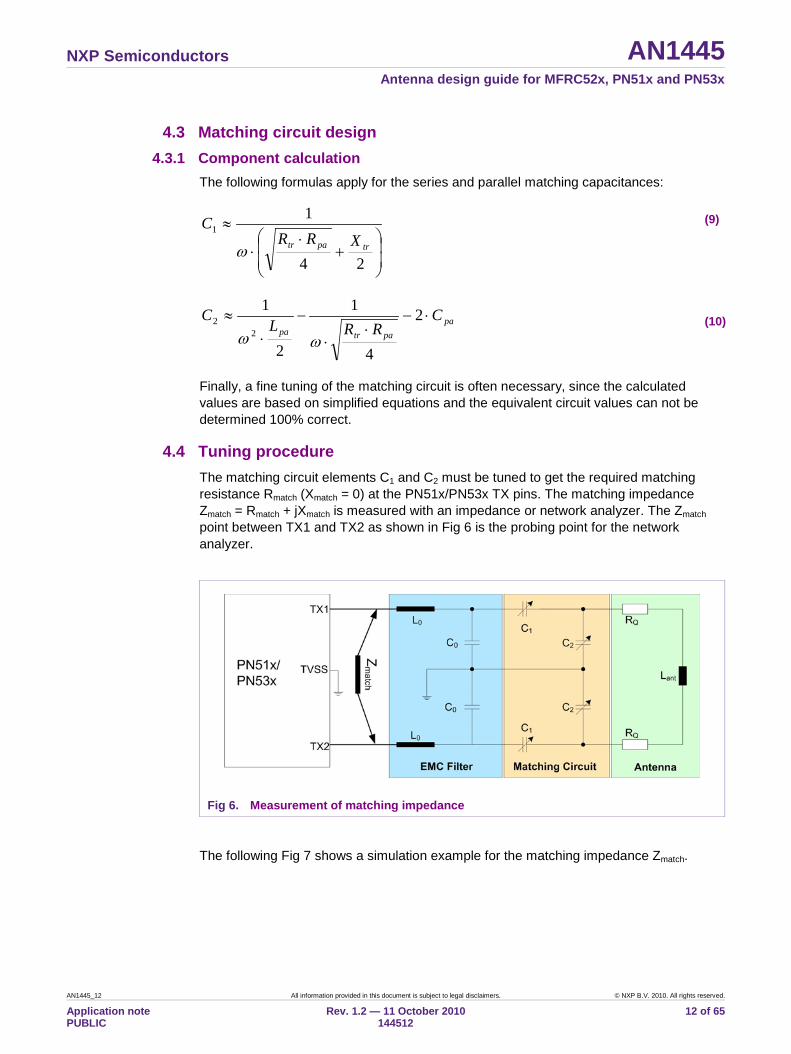
4.4 Tuning procedure The matching circuit elements C1 and C2 must be tuned to get the required matching resistance Rmatch (Xmatch = 0) at the PN51x/PN53x TX pins. The matching impedance Zmatch = Rmatch + jXmatch is measured with an impedance or network analyzer. The Zmatch point between TX1 and TX2 as shown in Fig 6 is the probing point for the network analyzer.
Fig 6. Measurement of matching impedance
The following Fig 7 shows a simulation example for the matching impedance Zmatch.
(9)
(10)

NXP Semiconductors AN1445 Antenna design guide for MFRC52x, PN51x and PN53x
AN1445_12 All information provided in this document is subject to legal disclaimers. © NXP B.V. 2010. All rights reserved.
Application note PUBLIC
Rev. 1.2 — 11 October 2010 144512
13 of 65
Fig 7. Calculation of matching impedance Fig 8 shows the smith chart simulation for Zmatch / 2:
Fig 8. Smith chart for matching impedance

NXP Semiconductors AN1445 Antenna design guide for MFRC52x, PN51x and PN53x
AN1445_12 All information provided in this document is subject to legal disclaimers. © NXP B.V. 2010. All rights reserved.
Application note PUBLIC
Rev. 1.2 — 11 October 2010 144512
14 of 65
Conditions for the tuning:
Rmatch curve symmetric around the operating frequency
Xmatch curve conjugate complex symmetric around the operating frequency
Note: All tuning and measurement of the antenna always has to be performed at the final mounting position to consider all parasitic effects like metal influence on quality factor, inductance and additional capacitance.
NXP Semiconductors AN1445 Antenna design guide for MFRC52x, PN51x and PN53x
AN1445_12 All information provided in this document is subject to legal disclaimers. © NXP B.V. 2010. All rights reserved.
Application note PUBLIC
Rev. 1.2 — 11 October 2010 144512
15 of 65
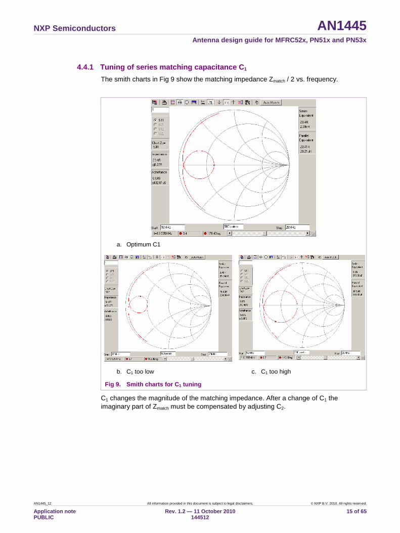
4.4.1 Tuning of series matching capacitance C1 The smith charts in Fig 9 show the matching impedance Zmatch / 2 vs. frequency.
a. Optimum C1
b. C1 too low c. C1 too high
Fig 9. Smith charts for C1 tuning
C1 changes the magnitude of the matching impedance. After a change of C1 the imaginary part of Zmatch must be compensated by adjusting C2.

NXP Semiconductors AN1445 Antenna design guide for MFRC52x, PN51x and PN53x
AN1445_12 All information provided in this document is subject to legal disclaimers. © NXP B.V. 2010. All rights reserved.
Application note PUBLIC
Rev. 1.2 — 11 October 2010 144512
16 of 65
4.5 Tuning of parallel matching capacitance C2 The smith charts show the matching impedance Zmatch / 2 vs. frequency.
d. Optimum C2
e. C2 too low f. C2 too high
Fig 10. Smith charts for C2 tuning
C2 changes mainly the imaginary part of Zmatch.

NXP Semiconductors AN1445 Antenna design guide for MFRC52x, PN51x and PN53x
AN1445_12 All information provided in this document is subject to legal disclaimers. © NXP B.V. 2010. All rights reserved.
Application note PUBLIC
Rev. 1.2 — 11 October 2010 144512
17 of 65
4.5.1 Tuning flow chart
Fig 11. Tuning flow chart
START
f Zmax > 13.56 MHz
Phase = 0 (+/- 10°)
Phase = 0 (+/- 10°)
Zmax = 40 - 50 Ohm
Zmax < 40 - 50 Ohm |Z(13.56 MHz - ∆ f)| = |Z(13.56 MHz + ∆ f)|
|Z(13.56 MHz - ∆ f)| <
|Z(13.56 MHz + ∆ f)|
TUNING OK
Increase C0
Decrease C0
NO Yes
Yes Increase C2 Decrease C2
Yes NO
NO
NO
Yes
Yes
NO NO
Decrease C1
Increase C1
Yes
NO
NXP Semiconductors AN1445 Antenna design guide for MFRC52x, PN51x and PN53x
AN1445_12 All information provided in this document is subject to legal disclaimers. © NXP B.V. 2010. All rights reserved.
Application note PUBLIC
Rev. 1.2 — 11 October 2010 144512
18 of 65
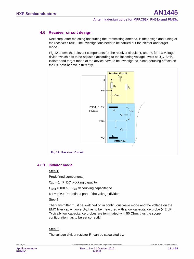
4.6 Receiver circuit design Next step, after matching and tuning the transmitting antenna, is the design and tuning of the receiver circuit. The investigations need to be carried out for initiator and target mode.
Fig 12 shows the relevant components for the receiver circuit. R1 and R2 form a voltage divider which has to be adjusted according to the incoming voltage levels at UC0. Both, Initiator and target mode of the device have to be investigated, since detuning effects on the RX path behave differently.
Fig 12. Receiver Circuit
4.6.1 Initiator mode
Predefined components:
Step 1:
CRX = 1 nF: DC blocking capacitor
Cvmid = 100 nF: Vmid decoupling capacitance
R1 = 1 kΩ: Predefined part of the voltage divider
The transmitter must be switched on in continuous wave mode and the voltage on the EMC filter capacitance UC0 has to be measured with a low capacitance probe (< 2 pF). Typically low capacitance probes are terminated with 50 Ohm, thus the scope configuration has to be set correctly!
Step 2:
The voltage divider resistor R2 can be calculated by:
Step 3:

NXP Semiconductors AN1445 Antenna design guide for MFRC52x, PN51x and PN53x
AN1445_12 All information provided in this document is subject to legal disclaimers. © NXP B.V. 2010. All rights reserved.
Application note PUBLIC
Rev. 1.2 — 11 October 2010 144512
19 of 65
−⋅= 10
12RX
C
UURR
with the target value of URX = 1 Vpp (antenna not detuned)
After inserting the determined resistor R2 the voltage on RX pin URX must be measured with a low capacitance probe (< 2 pF) for continuous transmitting mode.
Step 4:
The voltage URX must not exceed the maximum value URXmax even when the antenna is detuned by a target or passive card.
4.6.2 Target mode
The device must be placed in the test setup according to NFCIP1 test method standard. The magnetic field has to be increased continuously and the voltage on RX checked against the level URXmax.
Step 5:
URX < URXmax for H <= 7.5 A/m
If the voltage level on RX gets higher than the maximum value for field strength below 7.5 A/m, the resistor R2 must be increased to a value that meets the specification.
4.7 Example As an example the antenna of the PN51x/PN53x evaluation board Rev. 1.1 will be matched to the transmitter output.
Fig 13. PN51x/PN53x evaluation board antenna
The external RF components should be tuned to a value, that ITVDD ≈ 50mA.
Recommended Rmatch ≈ 50 Ohm
The series equivalent circuit of the antenna results to:
Ra = 1.9 Ohm
Ca = 11 pF
La= 2.9 µH
The calculation for the external damping resistor results to RQ = 2.57 Ohm. The chosen value for RQ is 3.3 Ohm and results in a Q-factor slightly below 30.
(11)

NXP Semiconductors AN1445 Antenna design guide for MFRC52x, PN51x and PN53x
AN1445_12 All information provided in this document is subject to legal disclaimers. © NXP B.V. 2010. All rights reserved.
Application note PUBLIC
Rev. 1.2 — 11 October 2010 144512
20 of 65
The parallel equivalent circuit of the antenna including quality factor damping resistors RQ = 3.3 Ohm is determined with the following values:
Rpa = 7148 Ohm
Cpa = 11 pF
Lpa= 2.9 µH
The EMC filter is determined with:
L0 = 560 nH
C0 = 220 pF
Calculation of Ztr:
Rtr = 217 Ohm
Xtr = -58 Ohm
Calculation of the matching parts C1, C2:
C1 = 19.8 pF -> 18 pF
C2 = 54.1 pF ->56 pF
For further component calculations please refer to the Excel-Worksheet “Antenna Topology I” in AN1444xx ([9]).
NXP Semiconductors AN1445 Antenna design guide for MFRC52x, PN51x and PN53x
AN1445_12 All information provided in this document is subject to legal disclaimers. © NXP B.V. 2010. All rights reserved.
Application note PUBLIC
Rev. 1.2 — 11 October 2010 144512
21 of 65
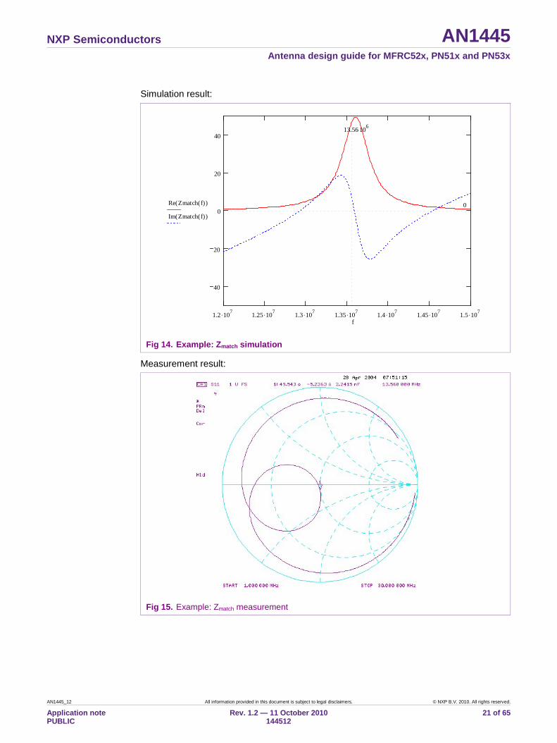
Simulation result:
Fig 14. Example: Zmatch simulation
Measurement result:
Fig 15. Example: Zmatch measurement
1.2 .107 1.25 .107 1.3 .107 1.35 .107 1.4 .107 1.45 .107 1.5 .107
40
20
0
20
40
0Re Zmatch f( )( )
Im Zmatch f( )( )
13.56 106⋅
f

NXP Semiconductors AN1445 Antenna design guide for MFRC52x, PN51x and PN53x
AN1445_12 All information provided in this document is subject to legal disclaimers. © NXP B.V. 2010. All rights reserved.
Application note PUBLIC
Rev. 1.2 — 11 October 2010 144512
22 of 65
5. Antenna Topology II This chapter introduces a capacitor split in the matching circuit to improve large voltage drops at the RX-path. The modifications in the antenna topology are show in Fig 17. The capacitor C1 at the TX1 pin from Antenna Topology I is replaced by two capacitors CS1 and CS2. The RX-Path is then connected in the middle of CS1 and CS2, which results in a more constant voltage behavior. The fine tuning of the circuit is equivalent to Antenna Topology I. Please refer to chapter 4.4 for fine tuning details.
5.1 Component calculation In order to calculate the values of the two capacitors, all other matching calculations have to be done before. To put it more precisely, the capacitor C1 has to be determined before changing the parts. The number of matching parts will not increase since CRX in Fig 17 can be removed after the performing the split of C1.
Fig 16. C1 Split Topology
Note: All tuning and measurement of the antenna always has to be performed at the final mounting position to consider all parasitic effects like metal influence on quality factor, inductance and additional capacitance.
Please also refer to the Excel-Worksheet “Antenna Topology II” in AN1444xx ([9]) for further component calculations.
To start changing the matching parts, first measure the voltage at VANT and VEMC of the Antenna Topology I with and without a target load. Place a 1k MIFARE card in the middle
NXP Semiconductors AN1445 Antenna design guide for MFRC52x, PN51x and PN53x
AN1445_12 All information provided in this document is subject to legal disclaimers. © NXP B.V. 2010. All rights reserved.
Application note PUBLIC
Rev. 1.2 — 11 October 2010 144512
23 of 65
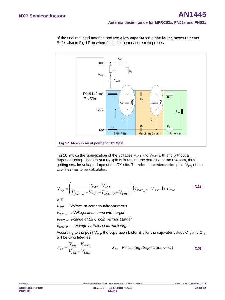
of the final mounted antenna and use a low capacitance probe for the measurements. Refer also to Fig 17 on where to place the measurement probes.
Fig 17. Measurement points for C1 Split
Fig 18 shows the visualization of the voltages VANT and VEMC with and without a target/detuning. The aim of a C1 split is to reduce the detuning at the RX-path, thus getting smaller voltage drops at the RX-site. Therefore, the intersection point Vavg of the two lines has to be calculated.
with
VANT … Voltage at antenna without target
VANT_D … Voltage at antenna with target
VEMC … Voltage at EMC point without target
VEMC_D … Voltage at EMC point with target
According to the point Vavg, the separation factor SC1 for the capacitor values C1S and C2S will be calculated as:
(12) ( ) EMCEMCDEMCEMCDEMCANTDANT
ANTEMCavg VVV
VVVVVV
V +−⋅
+−−−
= ___
(13) 1...11 CofSeperationPercentageSVVVV
S CEMCANT
EMCavgC −
−=

NXP Semiconductors AN1445 Antenna design guide for MFRC52x, PN51x and PN53x
AN1445_12 All information provided in this document is subject to legal disclaimers. © NXP B.V. 2010. All rights reserved.
Application note PUBLIC
Rev. 1.2 — 11 October 2010 144512
24 of 65
U_EMC; 5,10
U_EMC; 10,80
U_ANT; 24,14
U_ANT; 4,60
0,00
5,00
10,00
15,00
20,00
25,00
30,00
w ithout detuning w ith detuning
[V] U_EMC
U_ANT
(1) The intersection point is calculated with Vavg
Fig 18. Detuning at VEMC and VANT
The values for the two capacitors derived from the original C1 is:
Table 1 gives an example of the above made calculations with a value of 18 pF for C1.
Table 1. Example of C1-Split Measurements Values
UEMC without detuning 5,10 V
UEMC with detuning 10,80 V
UANT without detuning 24,14 V
UANT with detuning 4,60 V
Vavg 9,39 V
Percentage seperation of C1 22,58 %
C1S 79,71 pF
C2S 23,25 pF
(14) 1
11
CS S
CC =
12 1
1
CS S
CC−
= (15)
Vavg

NXP Semiconductors AN1445 Antenna design guide for MFRC52x, PN51x and PN53x
AN1445_12 All information provided in this document is subject to legal disclaimers. © NXP B.V. 2010. All rights reserved.
Application note PUBLIC
Rev. 1.2 — 11 October 2010 144512
25 of 65
Now choose appropriate values for C1S and C2S, such that the back transformation to a series capacitance gives C1 again. Thus, always check if
Otherwise the antenna will be mismatched. Replace only the capacitor C1 in the TX1-path as shown in Fig 17.
As an example, 78 pF for C1S and 23 pF for C2S has been chosen, which gives a total series capacitance of 17.76 pF for C1.
Note that the decoupling capacitor CRX was removed in the C1-split topology. See also Fig 17 on how to setup the C1-split.
Fig 19 shows the results by measuring again the voltages VRX and VANT with and without a load. It can be seen that the voltage swing on VRX with/without target load is much smaller than on a single C1 topology.
U_RX; 9,60
U_ANT; 24,14
U_ANT; 7,00U_RX; 9,50
0,00
5,00
10,00
15,00
20,00
25,00
30,00
w ithout detuning w ith detuning
[V] U_RX
U_ANT
Fig 19. The voltage at RX is more stabilized
SS
SS
CCCC
C21
211+⋅
≅ (16)

NXP Semiconductors AN1445 Antenna design guide for MFRC52x, PN51x and PN53x
AN1445_12 All information provided in this document is subject to legal disclaimers. © NXP B.V. 2010. All rights reserved.
Application note PUBLIC
Rev. 1.2 — 11 October 2010 144512
26 of 65
5.2 Features and hints of using antenna topology II By using the antenna topology II it is possible to counteract very strong voltage level variations on the RX-path in reader mode. Although there is no disadvantage in regard to communication constraints when using antenna topology II, it is trickier to tune it. In the worst case this means when using the antenna topology II, at least one more capacitor has to be reserved for the parallel capacitor C1. Remember, that both paths TX1 and TX2 have to be equal in component value. Thus, to retrieve full equivalence in the matching circuit, C1S combined with C2S needs to be equivalent to C1. The capacitance value of C1S and C2S can not always be achieved by a standard value. Mostly, a second capacitor placed in parallel to C1 (see Fig 20) or in parallel to both capacitors C1S and C2S has to be considered to get full symmetry.
Fig 20. Parallel capacitor to C1

NXP Semiconductors AN1445 Antenna design guide for MFRC52x, PN51x and PN53x
AN1445_12 All information provided in this document is subject to legal disclaimers. © NXP B.V. 2010. All rights reserved.
Application note PUBLIC
Rev. 1.2 — 11 October 2010 144512
27 of 65
6. Asymmetric tuning of antenna topology I or II The antenna topology I and II was tuned to have a matching of around 50 Ohms and an impedance curve symmetric around the operating frequency. When loaded with a target, the 13.56 MHz point shifts close to the short circuit point of the Smith Chart when strong detuning of the antenna occurs. Detuning effects arise when target(s) are placed above the reader device and load the reader antenna. The symmetric impedance curve of the antenna matching circuit may cause undesired communication failures.
One possibility to anticipate the effect of a short circuit at the real part of the impedance network is to tune the antenna matching asymmetric around the operating frequency (see Fig 21). The two resonance points of 13.56 MHz and 14.1 MHz still needs to be on the real axis of the smith chart but the crossing section moves up to the inductive part.
In order to move up the intersection point to the inductive part the capacitance C0 of the EMC filter has to be increased by about 50 pF when using the values as recommended in the example matching in chapter 4.7.
Fig 21 shows the smith chart of Zmatch vs. frequency of Antenna Topology I or II
Fig 21. Asymmetric tuning of antenna topology I and II

NXP Semiconductors AN1445 Antenna design guide for MFRC52x, PN51x and PN53x
AN1445_12 All information provided in this document is subject to legal disclaimers. © NXP B.V. 2010. All rights reserved.
Application note PUBLIC
Rev. 1.2 — 11 October 2010 144512
28 of 65
6.1 Tuning of series matching capacitance C1 The smith charts in Fig 22 shows the tuning effect on the impedance curve by adjusting C1.
Optimum C1
C1 too low C1 too high
Fig 22. Smith charts for C1 tuning

NXP Semiconductors AN1445 Antenna design guide for MFRC52x, PN51x and PN53x
AN1445_12 All information provided in this document is subject to legal disclaimers. © NXP B.V. 2010. All rights reserved.
Application note PUBLIC
Rev. 1.2 — 11 October 2010 144512
29 of 65
6.2 Tuning of parallel matching capacitance C2 The smith charts in Fig 23 shows the tuning effect on the impedance curve by adjusting C2.
Optimum C2
C1 too low C1 too high
Fig 23. Smith charts for C2 tuning
NXP Semiconductors AN1445 Antenna design guide for MFRC52x, PN51x and PN53x
AN1445_12 All information provided in this document is subject to legal disclaimers. © NXP B.V. 2010. All rights reserved.
Application note PUBLIC
Rev. 1.2 — 11 October 2010 144512
30 of 65
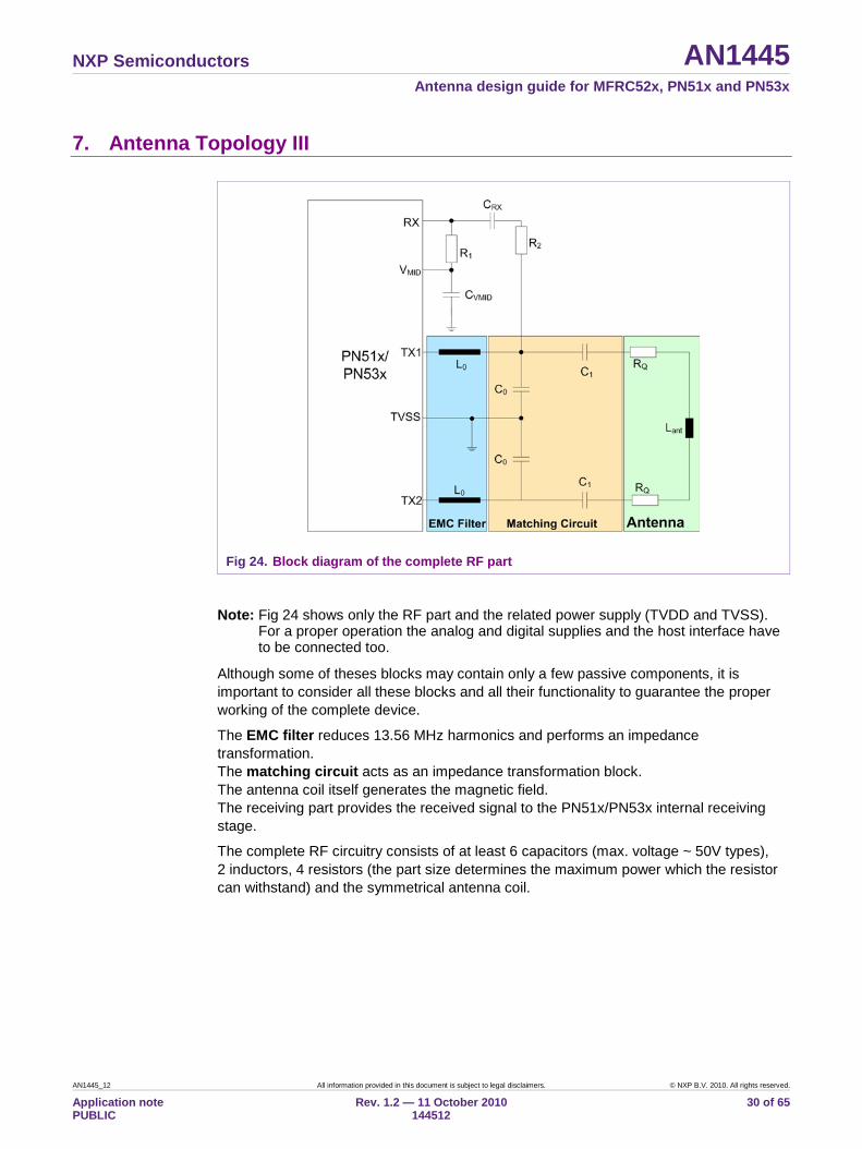
7. Antenna Topology III
Fig 24. Block diagram of the complete RF part
Note: Fig 24 shows only the RF part and the related power supply (TVDD and TVSS). For a proper operation the analog and digital supplies and the host interface have to be connected too.
Although some of theses blocks may contain only a few passive components, it is important to consider all these blocks and all their functionality to guarantee the proper working of the complete device.
The EMC filter reduces 13.56 MHz harmonics and performs an impedance transformation. The matching circuit acts as an impedance transformation block. The antenna coil itself generates the magnetic field. The receiving part provides the received signal to the PN51x/PN53x internal receiving stage.
The complete RF circuitry consists of at least 6 capacitors (max. voltage ~ 50V types), 2 inductors, 4 resistors (the part size determines the maximum power which the resistor can withstand) and the symmetrical antenna coil.

NXP Semiconductors AN1445 Antenna design guide for MFRC52x, PN51x and PN53x
AN1445_12 All information provided in this document is subject to legal disclaimers. © NXP B.V. 2010. All rights reserved.
Application note PUBLIC
Rev. 1.2 — 11 October 2010 144512
31 of 65
Table 2. Component list for a basic RF Design Abbreviation Explanation
RQ External damping resistors to adjust the quality factor. The power dissipation has to be considered.
C0, C1 Typically 0402, 0603 or 0805 SMD parts with low tolerance (< ±2%). NP0 dielectric is required for temperature stability reasons. The voltage limits has to be considered as well.
Cvmid, CRX X7R capacitor (< ±10%)
L0 Typically a small inductance with high Q factor for general applications. The frequency range and the maximum allowed current have to be considered. This inductance may be magnetically shielded.
R1, R2 0402, 0603 or 0805 SMD parts
NXP Semiconductors AN1445 Antenna design guide for MFRC52x, PN51x and PN53x
AN1445_12 All information provided in this document is subject to legal disclaimers. © NXP B.V. 2010. All rights reserved.
Application note PUBLIC
Rev. 1.2 — 11 October 2010 144512
32 of 65
7.1 Features and hints of antenna topology III The antenna topology in this document introduces some major advantages w.r.t. to power consumption, detuning effects on the RX-path and the type and amount of targets in the RF field.
The power consumption within the antenna topology described in chapter 4 “Antenna Topology I” is around 60 mA at TX-path. By changing to antenna topology III and tuning the resonance point around 70 Ω the power consumption becomes lower. The real and imaginary part of Zmatch change from symmetric to asymmetric around the operating frequency. The asymmetric impedance anticipates the detuning effect such that the magnitude of Zmatch stays closely constant when tags are in the field.
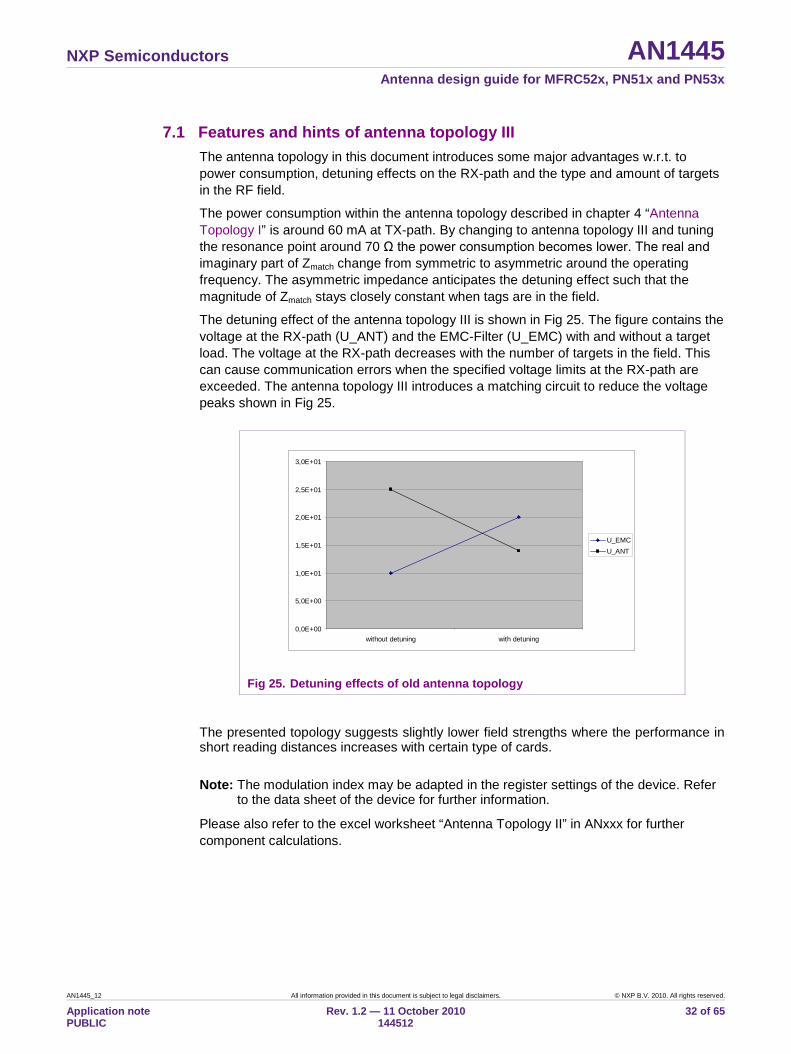
The detuning effect of the antenna topology III is shown in Fig 25. The figure contains the voltage at the RX-path (U_ANT) and the EMC-Filter (U_EMC) with and without a target load. The voltage at the RX-path decreases with the number of targets in the field. This can cause communication errors when the specified voltage limits at the RX-path are exceeded. The antenna topology III introduces a matching circuit to reduce the voltage peaks shown in Fig 25.
0,0E+00
5,0E+00
1,0E+01
1,5E+01
2,0E+01
2,5E+01
3,0E+01
without detuning with detuning
U_EMCU_ANT
Fig 25. Detuning effects of old antenna topology The presented topology suggests slightly lower field strengths where the performance in short reading distances increases with certain type of cards.
Note: The modulation index may be adapted in the register settings of the device. Refer to the data sheet of the device for further information.
Please also refer to the excel worksheet “Antenna Topology II” in ANxxx for further component calculations.

NXP Semiconductors AN1445 Antenna design guide for MFRC52x, PN51x and PN53x
AN1445_12 All information provided in this document is subject to legal disclaimers. © NXP B.V. 2010. All rights reserved.
Application note PUBLIC
Rev. 1.2 — 11 October 2010 144512
33 of 65
7.2 Transmitter matching resistance Rmatch The transmitter (TX) matching resistance Rmatch defines the equivalent resistance at the operating frequency present between the transmitter output pins TX1 and TX2 of the PN51x/PN53x. Different equivalent resistive loads lead to different transmitter current consumption.
7.2.1 Test circuit The following schematic in Fig 26 shows a possible configuration to investigate the optimum transmitter matching resistance Rmatch. The setup measures the available RF power Pant and the TX supply current ITVDD at different matching resistance values.
Fig 26. Test circuit for Rmatch
TX supply current vs. matching resistance
Fig 27 shows the TX supply current on the y-axis vs. the matching resistance on the x-axis in dependency on different supply voltages TVDD. An increase in Rmatch results in a lower current flow from TX and thus leads to a lower magnetical field generated by the antenna.
0,00
20,00
40,00
60,00
80,00
100,00
120,00
140,00
0,0 10,0 20,0 30,0 40,0 50,0 60,0 70,0 R match
TVDD [mA]
UTVDD = 2.5 V UTVDD = 3.0 V UTVDD = 3.5 V
Fig 27. Transmitter supply current vs. matching resistance
RF power vs. matching resistance
PN51x/ PN53x
L 0 TX1
TX2
TVSS C p C s
Balun 4:1
Spectrum Analyze r
50 Ohm C p,v
C s,v
C s C p,v
C s,v
C p L 0
200 Ohm R match
P ant TVDD
I TVDD U TVDD

NXP Semiconductors AN1445 Antenna design guide for MFRC52x, PN51x and PN53x
AN1445_12 All information provided in this document is subject to legal disclaimers. © NXP B.V. 2010. All rights reserved.
Application note PUBLIC
Rev. 1.2 — 11 October 2010 144512
34 of 65
Fig 28 shows antenna power (H-field) dissipation in relation to the matching resistance.
Fig 28. RF power vs. matching resistance
Power added efficiency @ 3V
Fig 29 shows the power added efficiency curve at different matching resistances of the antenna circuit.
Fig 29. Power added efficiency @ 3V
0,00
20,00
40,00
60,00
80,00
100,00
120,00
140,00
160,00
180,00
0,0 10,0 20,0 30,0 40,0 50,0 60,0 70,0 R match
P ant [mW]
UTVDD = 2.5 V UTVDD = 3.0 V UTVDD = 3.5 V
P ant =f(R match ) / PAE=f(R match ) / I TVDD =f(R match )
0,00
20,00
40,00
60,00
80,00
100,00
120,00
140,00
0,0 10,0 20,0 30,0 40,0 50,0 60,0 70,0 R match
P ant
[mW
] / P
AE
[%] /
ITV
DD
[mA
]
Pant PAE Itvdd
NXP Semiconductors AN1445 Antenna design guide for MFRC52x, PN51x and PN53x
AN1445_12 All information provided in this document is subject to legal disclaimers. © NXP B.V. 2010. All rights reserved.
Application note PUBLIC
Rev. 1.2 — 11 October 2010 144512
35 of 65
Conclusion
A higher matching resistance results in less power consumption but only slightly less available RF power output compared to the maximum available RF power output. A good compromise between available RF power and TX power consumption can be reached by a matching resistance Rmatch between 60 and 80 Ohm. The example matching circuit in chapter 7.7 has been tuned to 73 Ohm. Optimal Rmatch = 60 - 80 Ohm
7.3 Matching circuit design 7.3.1 Calculation of matching components
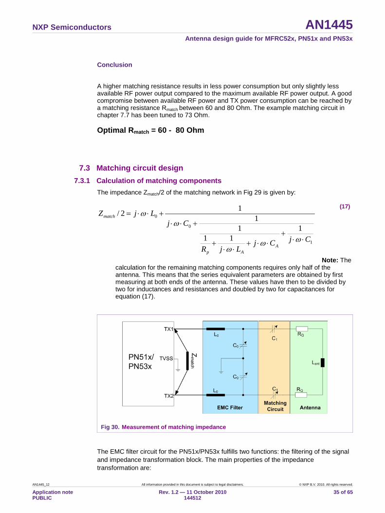
The impedance Zmatch/2 of the matching network in Fig 29 is given by:
Note: The calculation for the remaining matching components requires only half of the antenna. This means that the series equivalent parameters are obtained by first measuring at both ends of the antenna. These values have then to be divided by two for inductances and resistances and doubled by two for capacitances for equation (17).
Fig 30. Measurement of matching impedance
The EMC filter circuit for the PN51x/PN53x fulfills two functions: the filtering of the signal and impedance transformation block. The main properties of the impedance transformation are:
(17)
1
0
0
111
11
12/
CjCjLjR
CjLjZ
AAp
match
⋅⋅+
⋅⋅+⋅⋅
+
+⋅⋅+⋅⋅=
ωωω
ωω

NXP Semiconductors AN1445 Antenna design guide for MFRC52x, PN51x and PN53x
AN1445_12 All information provided in this document is subject to legal disclaimers. © NXP B.V. 2010. All rights reserved.
Application note PUBLIC
Rev. 1.2 — 11 October 2010 144512
36 of 65
• Decreasing the amplitude rise time after a modulation phase • Increasing the receiving bandwidth
The EMC filter and the matching circuit must transform the antenna impedance to the required TX matching resistance Zmatch at the operating frequency of f = 13.56 MHz.
The matching components C0 and C1 are determined by first measuring and then calculating the antenna impedance Zant.
The following formulas apply for Zant = Re(Zant)+Im(Zant):
2211
1
)Re(
⋅
−⋅+
=
AA
p
pant
LC
R
RZ
ωω
2211
1
)Im(
⋅
−⋅+
⋅−⋅
=
AA
p
AA
ant
LC
R
CL
Z
ωω
ωω
In order to solve the two unknown variables C0 and C1 in equation (17), the real part of the impedance network Zmatch is set to the matching resistance Rmatch = 73 Ohm and the imaginary part of Zmatch is set to 0. This is accomplished by extending the fraction in (17) with its complex conjugate, which is due to simplification reasons not carried out in this document.
(18)
(19)
22
0
1
)Re(73
)()Re()Re(73)Im(
1
antant
antant ZLZ
ZZ
C
−⋅⋅
+⋅⋅±⋅
=ω
ωω
⋅
⋅⋅+⋅
−⋅⋅
+⋅±
⋅+⋅
=ω
ω
ω
ωω
73)()Re()Re(73
)Re(73
)()Re()Re(73
)(73 20
22
0
20
20
0
LZZ
ZLZZ
LL
Cant
ant
antant
ant
(20)

NXP Semiconductors AN1445 Antenna design guide for MFRC52x, PN51x and PN53x
AN1445_12 All information provided in this document is subject to legal disclaimers. © NXP B.V. 2010. All rights reserved.
Application note PUBLIC
Rev. 1.2 — 11 October 2010 144512
37 of 65
Note: Due to simplification of the formulas and tolerances of the measured equivalent antenna circuit values, a final tuning of the matching circuit is necessary to achieve the required matching resistance at the transmitter output pins.
7.4 Tuning procedure The matching circuit elements C0 and C1 must be tuned to get the required matching resistance Rmatch (Xmatch = 0) at the PN51x/PN53x TX pins. The matching impedance Zmatch = Rmatch + jXmatch is measured with an impedance analyzer or network analyzer.
The following Fig 31 shows a simulation of the matching impedance Zmatch.
Fig 31. Simulation of matching impedance
Note: All tuning and measurement of the antenna has always to be performed at the final mounting position to consider all parasitic effects like metal influence on quality factor, inductance and additional capacitance.

NXP Semiconductors AN1445 Antenna design guide for MFRC52x, PN51x and PN53x
AN1445_12 All information provided in this document is subject to legal disclaimers. © NXP B.V. 2010. All rights reserved.
Application note PUBLIC
Rev. 1.2 — 11 October 2010 144512
38 of 65
The smith chart in Fig 32 shows the antenna simulation based on the example values used in chapter 7.7.
Fig 32. Smith chart for matching impedance

NXP Semiconductors AN1445 Antenna design guide for MFRC52x, PN51x and PN53x
AN1445_12 All information provided in this document is subject to legal disclaimers. © NXP B.V. 2010. All rights reserved.
Application note PUBLIC
Rev. 1.2 — 11 October 2010 144512
39 of 65
7.4.1 Tuning of EMC matching capacitance C0 The smith charts in Fig 33 show the matching impedance Zmatch vs. frequency.
Optimum C0
C0 too low C0 too high
Fig 33. Smith charts for C0 tuning
C0 changes the magnitude of the matching impedance. After a change of C0 the imaginary part of Zmatch needs to be compensated by adjusting C1.

NXP Semiconductors AN1445 Antenna design guide for MFRC52x, PN51x and PN53x
AN1445_12 All information provided in this document is subject to legal disclaimers. © NXP B.V. 2010. All rights reserved.
Application note PUBLIC
Rev. 1.2 — 11 October 2010 144512
40 of 65
7.4.2 Tuning of series matching capacitance C1 The smith charts in Fig 34 show the matching impedance Zmatch 2 vs. frequency.
Optimum C1
C1 too low C1 too high
Fig 34. Smith charts for C1 tuning
C1 changes mainly the imaginary part of Zmatch.

NXP Semiconductors AN1445 Antenna design guide for MFRC52x, PN51x and PN53x
AN1445_12 All information provided in this document is subject to legal disclaimers. © NXP B.V. 2010. All rights reserved.
Application note PUBLIC
Rev. 1.2 — 11 October 2010 144512
41 of 65
7.4.3 Tuning flow chart
Fig 35. Tuning flow chart
Note: The initial value of L0 has been set to 0.33 μH.
START
f Zmax > 13.56 MHz
Phase = 0 (+/- 10°)
Phase = 0 (+/- 10°)
Zmax = 60 - 80 Ohm
Zmax < 60 - 80 Ohm Phase(|Z(14.1 – 14.4 MHz )|)=0
TUNING OK
Increase L0
Decrease L0
NO Yes
Yes Increase C1 Decrease C1
Yes NO
NO
NO
Yes
Yes
NO NO
Increase C0
Decrease C0
Yes
NO
Phase(|Z(14.1 – 14.4 MHz )|)<0

NXP Semiconductors AN1445 Antenna design guide for MFRC52x, PN51x and PN53x
AN1445_12 All information provided in this document is subject to legal disclaimers. © NXP B.V. 2010. All rights reserved.
Application note PUBLIC
Rev. 1.2 — 11 October 2010 144512
42 of 65
7.5 Receiver circuit design Next step, after matching and tuning the transmitting antenna, is the design and tuning of the receiver circuit. The investigations need to be carried out for initiator and target mode.
Fig 36 shows the relevant components for the receiver circuit. R1 and R2 form a voltage divider which has to be adjusted according to the incoming voltage levels at UC0. Both, Initiator and Target mode of the device have to be investigated, since detuning effects on the RX path behave differently.
Fig 36. Receiver circuit
7.5.1 Initiator mode
Predefined components:
Step 1:
CRX = 1 nF: DC blocking capacitor
Cvmid = 100 nF: Vmid decoupling capacitance
R1 = 1 kΩ: Predefined part of the voltage divider
The transmitter must be switched on in continuous wave mode and the voltage on the EMC filter capacitance UC0 has to be measured with a low capacitance probe (< 2 pF).
Step 2:

NXP Semiconductors AN1445 Antenna design guide for MFRC52x, PN51x and PN53x
AN1445_12 All information provided in this document is subject to legal disclaimers. © NXP B.V. 2010. All rights reserved.
Application note PUBLIC
Rev. 1.2 — 11 October 2010 144512
43 of 65
Typically low capacitance probes are terminated with 50 Ohm, thus the scope configuration has to be set correctly!
The voltage divider resistor R2 can be calculated by:
Step 3:
−⋅= 10
12RX
C
UURR
with the target value of URX = 1 Vpp (antenna not detuned)
After inserting the determined resistor R2 the voltage on RX pin URX must be measured with a low capacitance probe (< 2 pF) for continuous transmitting mode.
Step 4:
The voltage URX must not exceed the maximum value URXmax even when the antenna is detuned by a target or passive card.
7.6 Target mode
The device must be placed in the test setup according to NFCIP1 test method standard. The magnetic field has to be increased continuously and the voltage on RX checked against the level URXmax.
Step 5:
URX < URXmax for H <= 7.5 A/m
If the voltage level on RX gets higher than the maximum value for field strength below 7.5 A/m, the resistor R2 must be increased to a value that meets the specification.
(21)
NXP Semiconductors AN1445 Antenna design guide for MFRC52x, PN51x and PN53x
AN1445_12 All information provided in this document is subject to legal disclaimers. © NXP B.V. 2010. All rights reserved.
Application note PUBLIC
Rev. 1.2 — 11 October 2010 144512
44 of 65
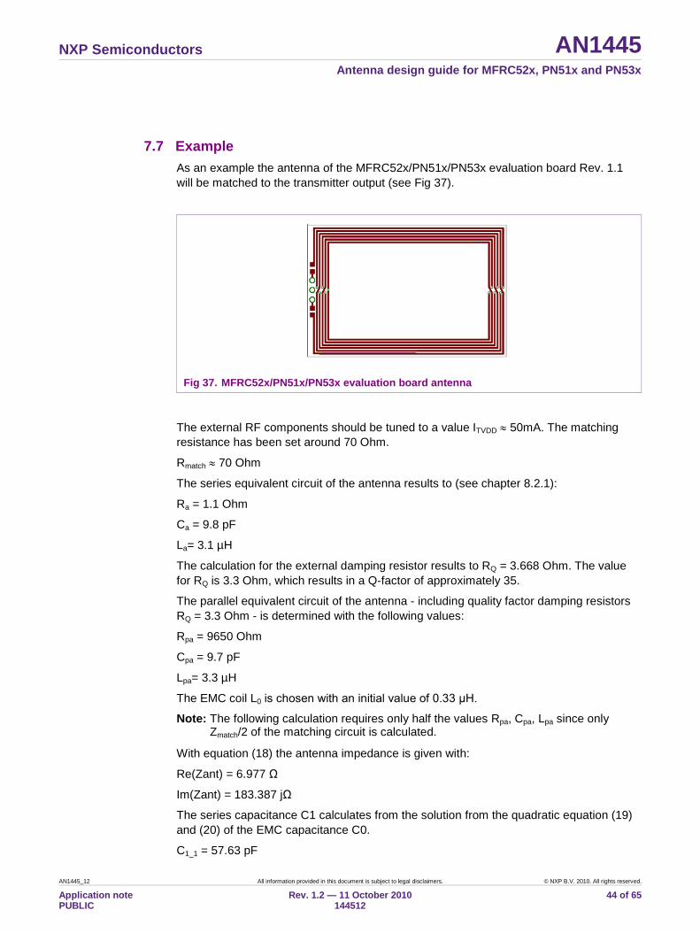
7.7 Example As an example the antenna of the MFRC52x/PN51x/PN53x evaluation board Rev. 1.1 will be matched to the transmitter output (see Fig 37).
Fig 37. MFRC52x/PN51x/PN53x evaluation board antenna
The external RF components should be tuned to a value ITVDD ≈ 50mA. The matching resistance has been set around 70 Ohm.
Rmatch ≈ 70 Ohm
The series equivalent circuit of the antenna results to (see chapter 8.2.1):
Ra = 1.1 Ohm
Ca = 9.8 pF
La= 3.1 µH
The calculation for the external damping resistor results to RQ = 3.668 Ohm. The value for RQ is 3.3 Ohm, which results in a Q-factor of approximately 35.
The parallel equivalent circuit of the antenna - including quality factor damping resistors RQ = 3.3 Ohm - is determined with the following values:
Rpa = 9650 Ohm
Cpa = 9.7 pF
Lpa= 3.3 µH
The EMC coil L0 is chosen with an initial value of 0.33 μH.
Note: The following calculation requires only half the values Rpa, Cpa, Lpa since only Zmatch/2 of the matching circuit is calculated.
With equation (18) the antenna impedance is given with:
Re(Zant) = 6.977 Ω
Im(Zant) = 183.387 jΩ
The series capacitance C1 calculates from the solution from the quadratic equation (19) and (20) of the EMC capacitance C0.
C1_1 = 57.63 pF

NXP Semiconductors AN1445 Antenna design guide for MFRC52x, PN51x and PN53x
AN1445_12 All information provided in this document is subject to legal disclaimers. © NXP B.V. 2010. All rights reserved.
Application note PUBLIC
Rev. 1.2 — 11 October 2010 144512
45 of 65
C1_2 = 71.95 pF
The EMC capacitances C0_1 and C0_2 are determined for the values of C1_1 and C1_2:
C0_1 = -417.62 pF
C0_2 = 618.20 pF
The correct values for the matching components are C1_2 and C0_2.
Refer to Fig 31 for a simulation of the magnitude and phase of the final antenna circuit.
The smith chart in Fig 38 was captured with a network analyzer showing a matching at 72 Ohm with the given values above.
Fig 38. Zmatch simulation

NXP Semiconductors AN1445 Antenna design guide for MFRC52x, PN51x and PN53x
AN1445_12 All information provided in this document is subject to legal disclaimers. © NXP B.V. 2010. All rights reserved.
Application note PUBLIC
Rev. 1.2 — 11 October 2010 144512
46 of 65
8. Appendix
8.1 Antenna design 8.1.1 Antenna inductance
The following two sub-chapters 8.1.2 and 8.1.3 show required formulas to estimate the antenna inductance in free air.
Note: Sophisticated simulation software is required to calculate the antennas parameters to estimate antenna values in environments containing metal (such as shielding planes or batteries in devices).
8.1.2 Circular antennas Fig 39 shows the profile a typical circular antenna.
D
s
Fig 39. Circular antenna
The inductance can be estimated using the following formula:
[ ][ ][ ]cmDcms
cmDNnHL aa
⋅+
⋅⋅=
75.21
6.24][2
D Average antenna diameter
s Antenna width
Na Number of turns
(22)

NXP Semiconductors AN1445 Antenna design guide for MFRC52x, PN51x and PN53x
AN1445_12 All information provided in this document is subject to legal disclaimers. © NXP B.V. 2010. All rights reserved.
Application note PUBLIC
Rev. 1.2 — 11 October 2010 144512
47 of 65
8.1.3 Rectangular antennas Fig 40 shows a typical rectangular antenna.
gw
b0
a0
bavg
aavg
Fig 40. Rectangular antenna Variables: ao, bo Overall dimensions of the coil aavg, bavg Average dimensions of the coil t Track thickness w Track width g Gap between tracks Na Number of turns d Equivalent diameter of the track The inductance can be calculated by:
[ ] 8.14321
0aa NxxxxL ⋅+−+⋅=
πµ
With:
( )π
wtd +⋅=
2
( )wgNaa aoavg +⋅−= ( )wgNbb aoavg +⋅−=
++⋅
⋅⋅⋅=
221
2ln
avgavgavg
avgavgavg
baad
baax
++⋅
⋅⋅⋅=
222
2ln
avgavgavg
avgavgavg
babd
babx
(23)
NXP Semiconductors AN1445 Antenna design guide for MFRC52x, PN51x and PN53x
AN1445_12 All information provided in this document is subject to legal disclaimers. © NXP B.V. 2010. All rights reserved.
Application note PUBLIC
Rev. 1.2 — 11 October 2010 144512
48 of 65
+−+⋅= 22
3 2 avgavgavgavg babax 44
avgavg bax
+=
8.1.4 Number of turns Depending on the antenna size, the number of turns has to be chosen in a way to achieve an antenna inductance between 300 nH and 3 µH.
The parasitic capacitance should be kept as low as possible to achieve a self-resonance frequency > 35 MHz.
A typical the number of turns will be in the range
Na=1 – 6,
which is suitable for various applications and antenna sizes.
Due to the coupling coefficient, a low number of turns are preferred. The lower the numbers of turns, the lower is the influence of coupled devices (e.g. 2nd NFC device, Card, Reader) to the 1st device. This also means that the detuning effect on the 1st device is minimized when reducing the distance between the two devices. The overall performance loss due to low number of turns is negligible.
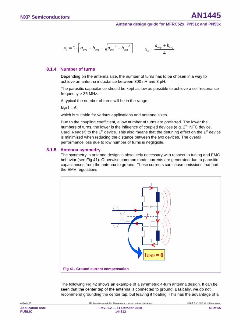
8.1.5 Antenna symmetry The symmetry in antenna design is absolutely necessary with respect to tuning and EMC behavior (see Fig 41). Otherwise common mode currents are generated due to parasitic capacitances from the antenna to ground. These currents can cause emissions that hurt the EMV regulations
Fig 41. Ground current compensation
The following Fig 42 shows an example of a symmetric 4-turn antenna design. It can be seen that the center tap of the antenna is connected to ground. Basically, we do not recommend grounding the center tap, but leaving it floating. This has the advantage of a

NXP Semiconductors AN1445 Antenna design guide for MFRC52x, PN51x and PN53x
AN1445_12 All information provided in this document is subject to legal disclaimers. © NXP B.V. 2010. All rights reserved.
Application note PUBLIC
Rev. 1.2 — 11 October 2010 144512
49 of 65
virtual ground point which is floating to achieve symmetry of the antenna. Refer also to Fig 41 where center tap is not connected.
Fig 42. Example symmetric 4-turn antenna
8.1.6 Ferrite shielding The benefit of a ferrite is to shield an antenna against the influence of metal. A metal plane could be part of the housing of the device or a ground plane of the device PCB itself, which has to be connected very near to the antenna. If metal is placed very near to the antenna the alternating magnetic field generates eddy currents in the metal. These eddy currents absorb power, and lead to detuning of the antenna due to a decreased inductance and quality factor. Therefore, it is necessary to shield the antenna with ferrite for proper operation in close metallic environment.
The following examples should give an estimation about the influence of ferrite to the distribution of the magnetic field.
A circular antenna has been used to simplify the simulation. A circular antenna is rotational symmetric to the x-axis. Therefore, the simulation can be reduced to a two dimensional mathematical problem. The simulation estimates the field distribution of a non-disturbed antenna. It has been assumed an antenna radius of 7.5 cm with 1 turn and a copper wire of 1mm thickness.
Fig 43 shows the two-dimensional magnetic field of the circular antenna.
The right part shows the field distribution. The highest field strength is generated in the area of the coil.
The left part shows the magnitude of the field strength H over the distance d. The minimal field strength of HMIN = 1.5 A/m defined by ISO/IEC 14443 is marked with doted vertical line.
Note: The shielding effect of the ferrite strongly depends on the ferrite material and the distance between antenna and influencing material. The shielding effect may be negligible if the antenna is very near to interfering material (metal, battery) and the ferrite has low permeability (foils usually µR<10).
TVSS

NXP Semiconductors AN1445 Antenna design guide for MFRC52x, PN51x and PN53x
AN1445_12 All information provided in this document is subject to legal disclaimers. © NXP B.V. 2010. All rights reserved.
Application note PUBLIC
Rev. 1.2 — 11 October 2010 144512
50 of 65
Fig 43. Non disturbed field distribution of a circular antenna
Fig 44 shows the field distribution of the defined antenna but a metal plane near to the antenna. The magnitude of the field strength has decreased compared to the disturbed field which leads to a decreased operating distance.
026 4
5 cm
Minimum field strength
Hmin=1.5 A/m
Field strengthcolor map
metal plane
d
|H| [A/m]
Fig 44. Field distribution of a circular antenna with a metal plane
026 4
d
7.5 cm
Minimum field strengthHmin=1.5 A/m
Field strengthcolor map
|H| [A/m]

NXP Semiconductors AN1445 Antenna design guide for MFRC52x, PN51x and PN53x
AN1445_12 All information provided in this document is subject to legal disclaimers. © NXP B.V. 2010. All rights reserved.
Application note PUBLIC
Rev. 1.2 — 11 October 2010 144512
51 of 65
Fig 45 shows a ferrite plane (µR=40) which is positioned between the metal plane and the antenna coil itself. The field strength very near to the ferrite increases, but the increasing magnitude does not necessarily result in an increase of the operating distance at HMIN value (vertical doted line).
Fig 45. Ferrite shielded field distribution of a circular antenna
The simulation shows that the use of a ferrite reduces the generated eddy currents in a metal plane. The ferrite generates an additional field component, which results in a fixed detuning of the antenna itself.
8.1.7 Antenna quality factor The quality factor is a determining constraint to design and tune an antenna. Fig 46 shows an excerpt of a typical 100% ASK modulation. The maximum timing limit of 3us (as defined in the ISO/IEC14443) for a modulation pause is taken to calculate the quality factor.
Fig 46. Pulse width definition
026 4
d
7.5 cm
Minimum field strength
Hmin=1.5 A/m
Field strengthcolor map
metal planeferrite plane
T = 3 µs

NXP Semiconductors AN1445 Antenna design guide for MFRC52x, PN51x and PN53x
AN1445_12 All information provided in this document is subject to legal disclaimers. © NXP B.V. 2010. All rights reserved.
Application note PUBLIC
Rev. 1.2 — 11 October 2010 144512
52 of 65
The bandwidth B –pulse width T product is defined as:
1≥⋅TB
With the bandwidth definition
QfB =
the B-T product results to
Note: The recommended antenna quality factor is Qa = 35.
(24)
(25)
68.40356.13
≤µ⋅≤
⋅≤
QsMHzQ
TfQ

NXP Semiconductors AN1445 Antenna design guide for MFRC52x, PN51x and PN53x
AN1445_12 All information provided in this document is subject to legal disclaimers. © NXP B.V. 2010. All rights reserved.
Application note PUBLIC
Rev. 1.2 — 11 October 2010 144512
53 of 65
8.2 Equivalent circuit 8.2.1 Determination of series equivalent circuit
The antenna loop has to be connected to an impedance analyzer to measure the series equivalent components.
Note: The equivalent circuit (see Fig 47) must be determined under final environmental conditions especially if the antenna will be operated in metal environment or a ferrite will be used for shielding.
Antenna
Ra
La
Ca
Fig 47. Series equivalent circuit
Typical values:
La = 0.3...3 µH
Ca = 3...30 pF
Ra = 0.3...8 Ω
8.2.2 Calculation of antenna quality factor damping resistor RQ The quality factor of the antenna is
a
aa R
LQ ⋅=ω
If the calculated value of Qa is higher than the target value of 35, an external damping resistor RQ has to be inserted on each antenna side to reduce the Q-factor to a value of 35 (±10%).
The value of RQ calculates as:
−
⋅⋅= a
aQ RLR
355.0 ω
(26)
(27)

NXP Semiconductors AN1445 Antenna design guide for MFRC52x, PN51x and PN53x
AN1445_12 All information provided in this document is subject to legal disclaimers. © NXP B.V. 2010. All rights reserved.
Application note PUBLIC
Rev. 1.2 — 11 October 2010 144512
54 of 65
8.2.3 Determination of parallel equivalent circuit The parallel equivalent circuit of the antenna together with the added external damping resistor RQ has to be measured. The quality factor should be checked again to be sure to achieve the required value of Q=35.
Note: The equivalent circuit (Fig 48) must be determined under final environmental conditions especially if the antenna will be operated in metal environment or a ferrite will be used for shielding.
Antenna
RQ
RQ
Rpa LpaCpa
Fig 48. Parallel equivalent circuit
The following formula applies:
Qa
apa
apa
apa
RRLR
CCLL
⋅+⋅
=
=
=
2)(
ˆ
ˆˆ
2ω
(28)

NXP Semiconductors AN1445 Antenna design guide for MFRC52x, PN51x and PN53x
AN1445_12 All information provided in this document is subject to legal disclaimers. © NXP B.V. 2010. All rights reserved.
Application note PUBLIC
Rev. 1.2 — 11 October 2010 144512
55 of 65
8.3 Equivalent circuit measurement 8.3.1 Impedance analyzer with equivalent circuit calculation
Impedance analyzers like Agilent 4294A or 4395A can determine directly the series or parallel equivalent circuit by measuring the magnitude and the phase of the impedance of the connected antenna.
Note: The antenna has to be at the final mounting position to consider all parasitic effects like metal influence on quality factor, inductance and additional capacitance.
The antenna needs to be connected to the analyzer by using an appropriate test fixture that does not influence any antenna parameters.
The analyzer has to be calibrated (open, short and load compensation at the calibration plane) and the test fixture needs to be compensated (open, short compensation at the connection points) before each measurement. Please refer to device manual on how to carry out these steps.
Settings: Θ,Z
Start frequency: 1 MHz
Stop frequency: above self-resonance frequency of the antenna
Advantage: • Fast and simple method
Disadvantages: • Additional equipment required • Low accuracy of the measurement which especially results from the loss resistance
for high quality factor coils (Qpc > 60).
8.3.2 Network analyzer This section briefly describes the determination of the antenna equivalent circuit using a network analyzer without any equivalent circuit functionality.
Note: The antenna has to be at the final mounting position to consider all parasitic effects like metal influence on quality factor, inductance and additional capacitance.
The antenna needs to be connected to the analyzer by using an appropriate test fixture that does not influence the antenna parameters.
The analyzer has to be calibrated (open, short and load compensation at the calibration plane) and the test fixture needs to be compensated (open, short compensation at the connection points) before each measurement. Please refer to device manual on how to carry out these steps.
Settings: S11,
Chart: Smith Z
Start frequency: 1 MHz

NXP Semiconductors AN1445 Antenna design guide for MFRC52x, PN51x and PN53x
AN1445_12 All information provided in this document is subject to legal disclaimers. © NXP B.V. 2010. All rights reserved.
Application note PUBLIC
Rev. 1.2 — 11 October 2010 144512
56 of 65
Stop frequency: above self-resonance frequency of the antenna
8.3.3 Series equivalent circuit The following characteristic circuit elements can be determined by measurements at characteristic points (see also Fig 47 for series equivalent circuit).
Rs Equivalent resistance at f = 1 MHz
La Equivalent inductance at f = 1 MHz
Rp Equivalent resistance at the self-resonance frequency
fra Self-resonance frequency of the antenna
The antenna capacitance Ca can be calculated with:
( ) ara
a LfC 22
1⋅⋅
=π
The following Fig 49 shows simulation results to determine the characteristic circuit.
g. Rs = 0.82 Ohm, La = 2.99 µH h. Rp = 18 kOhm, fra = 29.14 MHz
Fig 49. Simulation results for characteristic circuit
The series equivalent resistance of the antenna (see Fig 50) at the operating frequency fop = 13.56 MHz can be calculated out of the characteristic circuit with:
(29)

NXP Semiconductors AN1445 Antenna design guide for MFRC52x, PN51x and PN53x
AN1445_12 All information provided in this document is subject to legal disclaimers. © NXP B.V. 2010. All rights reserved.
Application note PUBLIC
Rev. 1.2 — 11 October 2010 144512
57 of 65
Fig 50. Series equivalent resistance calculation
( )p
aopsa R
LfRR
22 ⋅⋅⋅+=
π
The parallel equivalent circuit always has to be calculated by means of the series equivalent circuit using equation (28).
(30)
Ra
La
Ca
Rs
La
Ca Rp

NXP Semiconductors AN1445 Antenna design guide for MFRC52x, PN51x and PN53x
AN1445_12 All information provided in this document is subject to legal disclaimers. © NXP B.V. 2010. All rights reserved.
Application note PUBLIC
Rev. 1.2 — 11 October 2010 144512
58 of 65
8.4 Pulse shape check The following pulse shape checks are a quick way for investigating the shaping of the generated RF-field. The figures in 8.5 always relates to the latest ISO/IEC18092 specification.
The correct measurement techniques needs to be carried out in ISO/IEC 22536 (NFCIP – RF Interface Test methods) and/or ISO/IEC 10373-6 (Identification cards – Test methods) and ISO/IEC14443!
The Q-factor can be checked by using the fact that the Q-factor has a direct influence on the edges of the modulation shape.
An oscilloscope with a bandwidth of at least 50 MHz has to be used to carry out the module shape measurements (Fig 51).
Fig 51. Setup to check the Q-factor
CH1: Use a loop with the ground line shortcut at the probe to enable inductive signal coupling. Hold the probe loop closely above the antenna.
CH2: Used as trigger signal by using Sigout (See [1]-[4] for reference documents)
It is recommended to check the pulse shape according to the values given in Fig 52 and Fig 52.
Note: The absolute measured voltage in CH1 depends on the coupling (= distance) between the probe loop and the reader antenna. The influence of the coupling on the shape can be neglected. The complete antenna tuning and Q-checking is done without any card.
PHILIPS
Antenna
ReaderTerminal
NXP Semiconductors AN1445 Antenna design guide for MFRC52x, PN51x and PN53x
AN1445_12 All information provided in this document is subject to legal disclaimers. © NXP B.V. 2010. All rights reserved.
Application note PUBLIC
Rev. 1.2 — 11 October 2010 144512
59 of 65
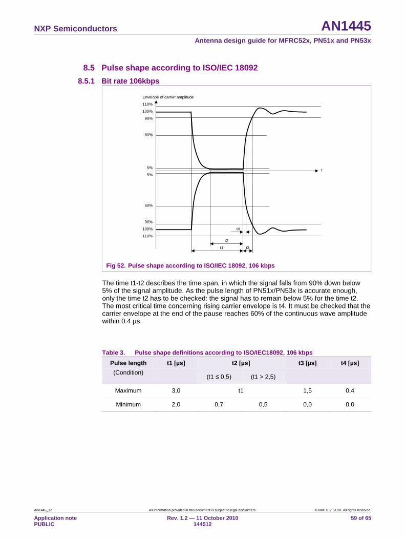
8.5 Pulse shape according to ISO/IEC 18092 8.5.1 Bit rate 106kbps
Fig 52. Pulse shape according to ISO/IEC 18092, 106 kbps The time t1-t2 describes the time span, in which the signal falls from 90% down below 5% of the signal amplitude. As the pulse length of PN51x/PN53x is accurate enough, only the time t2 has to be checked: the signal has to remain below 5% for the time t2. The most critical time concerning rising carrier envelope is t4. It must be checked that the carrier envelope at the end of the pause reaches 60% of the continuous wave amplitude within 0.4 µs.
Table 3. Pulse shape definitions according to ISO/IEC18092, 106 kbps Pulse length (Condition)
t1 [µs] t2 [µs] t3 [µs] t4 [µs]
(t1 ≤ 0,5) (t1 > 2,5)
Maximum 3,0 t1 1,5 0,4
Minimum 2,0 0,7 0,5 0,0 0,0
110% 100% 90%
5%
60%
5%
60%
90% 100% 110%
t4
t2 t1 t3
Envelope of carrier amplitude
t

NXP Semiconductors AN1445 Antenna design guide for MFRC52x, PN51x and PN53x
AN1445_12 All information provided in this document is subject to legal disclaimers. © NXP B.V. 2010. All rights reserved.
Application note PUBLIC
Rev. 1.2 — 11 October 2010 144512
60 of 65
8.5.2 Bit rate 212 kbps and 424 kbps
Fig 53. Pulse shape according to ISO/IEC 18092, 212 and 424 kbps
Table 4. Table 8-1: Pulse shape definitions according to ISO/IEC18092, 212 and 424 kbps 212 kbps 424 kbps
tf 2,0 µs max 1,0 µs max
tr 2,0 µs max 1,0 µs max
y 0,1 (a-b) 0,1 (a-b)
hf, hr 0,1 (a-b) max 0,1 (a-b) max

NXP Semiconductors AN1445 Antenna design guide for MFRC52x, PN51x and PN53x
AN1445_12 All information provided in this document is subject to legal disclaimers. © NXP B.V. 2010. All rights reserved.
Application note PUBLIC
Rev. 1.2 — 11 October 2010 144512
61 of 65
9. References [1] Data sheet: PN511 Transmission Module (Doc. No.: 0797xx)
[2] Data sheet: PN512 Transmission Module (Doc. No.: 1113xx)
[3] Data sheet: PN531 Transmission Module (Doc. No.: 1119xx)
[4] Data sheet: PN532 Transmission Module (Doc. No.:1154xx)
[5] Ecma 340 NFCIP-1 Interface and protocol
[6] ISO/IEC 18092: Near Field Communication – Interface and Protocol (NFCIP-1)
[7] MathCAD 13
[8] RFSim99
[9] NFC Transmission Module Antenna and RF Design Guide - Addon - Excel Calculation (Doc. No.: 1444xx)
[10] ISO/IEC 10373-6
[11] ISO/IEC 22536
[12] ISO/IEC 14443
[13] RF amplifier for NXP’s contactless NFC Reader IC’s (Doc. No.: 1425xx)
[14] Datasheet MFRC523, Contactless Reader IC
[15] Datasheet MFRC522, Contactless Reader IC
10. Abbreviations EMC Electromagnetic compatibility IC Integrated circuit NFC Near field communication PCB Printed circuit board Rmatch Transmitter matching resistance RF Radio frequency RFID Radio frequency identification RX Receiver TX Transmitter Zmatch Transmitter matching impedance

U
nknown docum
ent property nam
e.
Error! Unknow
n document property nam
e.Error! Unknow
n document property nam
e. Error! U
nknown docum
ent property
NXP Semiconductors AN1445 Antenna design guide for MFRC52x, PN51x and PN53x
AN1445_12 All information provided in this document is subject to legal disclaimers. © NXP B.V. 2010. All rights reserved.
Application note PUBLIC
Rev. 1.2 — 11 October 2010 144512
62 of 65
11. Legal information
11.1 Definitions Draft — The document is a draft version only. The content is still under internal review and subject to formal approval, which may result in modifications or additions. NXP Semiconductors does not give any representations or warranties as to the accuracy or completeness of information included herein and shall have no liability for the consequences of use of such information.
11.2 Disclaimers Limited warranty and liability — Information in this document is believed to be accurate and reliable. However, NXP Semiconductors does not give any representations or warranties, expressed or implied, as to the accuracy or completeness of such information and shall have no liability for the consequences of use of such information.
In no event shall NXP Semiconductors be liable for any indirect, incidental, punitive, special or consequential damages (including - without limitation - lost profits, lost savings, business interruption, costs related to the removal or replacement of any products or rework charges) whether or not such damages are based on tort (including negligence), warranty, breach of contract or any other legal theory.
Notwithstanding any damages that customer might incur for any reason whatsoever, NXP Semiconductors’ aggregate and cumulative liability towards customer for the products described herein shall be limited in accordance with the Terms and conditions of commercial sale of NXP Semiconductors.
Right to make changes — NXP Semiconductors reserves the right to make changes to information published in this document, including without limitation specifications and product descriptions, at any time and without notice. This document supersedes and replaces all information supplied prior to the publication hereof.
Suitability for use — NXP Semiconductors products are not designed, authorized or warranted to be suitable for use in life support, life-critical or safety-critical systems or equipment, nor in applications where failure or malfunction of an NXP Semiconductors product can reasonably be expected to result in personal injury, death or severe property or environmental damage. NXP Semiconductors accepts no liability for inclusion and/or use of NXP Semiconductors products in such equipment or applications and therefore such inclusion and/or use is at the customer’s own risk.
Applications — Applications that are described herein for any of these products are for illustrative purposes only. NXP Semiconductors makes no representation or warranty that such applications will be suitable for the specified use without further testing or modification.
Customers are responsible for the design and operation of their applications and products using NXP Semiconductors products, and NXP Semiconductors accepts no liability for any assistance with applications or customer product design. It is customer’s sole responsibility to determine whether the NXP Semiconductors product is suitable and fit for the customer’s applications and products planned, as well as for the planned application and use of customer’s third party customer(s). Customers should provide appropriate design and operating safeguards to minimize the risks associated with their applications and products.
NXP Semiconductors does not accept any liability related to any default, damage, costs or problem which is based on any weakness or default in the customer’s applications or products, or the application or use by customer’s third party customer(s). Customer is responsible for doing all necessary
testing for the customer’s applications and products using NXP Semiconductors products in order to avoid a default of the applications and the products or of the application or use by customer’s third party customer(s). NXP does not accept any liability in this respect.
Export control — This document as well as the item(s) described herein may be subject to export control regulations. Export might require a prior authorization from national authorities.
Evaluation products — This product is provided on an “as is” and “with all faults” basis for evaluation purposes only. NXP Semiconductors, its affiliates and their suppliers expressly disclaim all warranties, whether express, implied or statutory, including but not limited to the implied warranties of non-infringement, merchantability and fitness for a particular purpose. The entire risk as to the quality, or arising out of the use or performance, of this product remains with customer.
In no event shall NXP Semiconductors, its affiliates or their suppliers be liable to customer for any special, indirect, consequential, punitive or incidental damages (including without limitation damages for loss of business, business interruption, loss of use, loss of data or information, and the like) arising out the use of or inability to use the product, whether or not based on tort (including negligence), strict liability, breach of contract, breach of warranty or any other theory, even if advised of the possibility of such damages.
Notwithstanding any damages that customer might incur for any reason whatsoever (including without limitation, all damages referenced above and all direct or general damages), the entire liability of NXP Semiconductors, its affiliates and their suppliers and customer’s exclusive remedy for all of the foregoing shall be limited to actual damages incurred by customer based on reasonable reliance up to the greater of the amount actually paid by customer for the product or five dollars (US$5.00). The foregoing limitations, exclusions and disclaimers shall apply to the maximum extent permitted by applicable law, even if any remedy fails of its essential purpose.
11.3 Licenses Purchase of NXP ICs with ISO/IEC 14443 type B functionality
This NXP Semiconductors IC is ISO/IEC 14443 Type B software enabled and is licensed under Innovatron’s Contactless Card patents license for ISO/IEC 14443 B.
The license includes the right to use the IC in systems and/or end-user equipment.
RATP/Innovatron Technology
11.4 Trademarks Notice: All referenced brands, product names, service names and trademarks are property of their respective owners.
MIFARE— is a trademark of NXP B.V.

NXP Semiconductors AN1445 Antenna design guide for MFRC52x, PN51x and PN53x
AN1445_12 All information provided in this document is subject to legal disclaimers. © NXP B.V. 2010. All rights reserved.
Application note PUBLIC
Rev. 1.2 — 11 October 2010 144512
63 of 65
12. List of figures
Fig 1. Block diagram of the complete RF part ............. 7Fig 2. Series equivalent circuit .................................... 8Fig 3. Parallel equivalent circuit .................................. 9Fig 4. Impedance transformation ................................ 9Fig 5. Definition of transformation impedance Ztr ...... 10Fig 6. Measurement of matching impedance ............ 12Fig 7. Calculation of matching impedance ................ 13Fig 8. Smith chart for matching impedance ............... 13Fig 9. Smith charts for C1 tuning ............................... 15Fig 10. Smith charts for C2 tuning ............................... 16Fig 11. Tuning flow chart ............................................. 17Fig 12. Receiver Circuit ............................................... 18Fig 13. PN51x/PN53x evaluation board antenna ........ 19Fig 14. Example: Zmatch simulation .............................. 21Fig 15. Example: Zmatch measurement ........................ 21Fig 16. C1 Split Topology ............................................ 22Fig 17. Measurement points for C1 Split ..................... 23Fig 18. Detuning at VEMC and VANT .............................. 24Fig 19. The voltage at RX is more stabilized ............... 25Fig 20. Parallel capacitor to C1 ................................... 26Fig 21. Asymmetric tuning of antenna topology I and II
........................................................................ 27Fig 22. Smith charts for C1 tuning ............................... 28Fig 23. Smith charts for C2 tuning ............................... 29Fig 24. Block diagram of the complete RF part ........... 30Fig 25. Detuning effects of old antenna topology ........ 32Fig 26. Test circuit for Rmatch ....................................... 33Fig 27. Transmitter supply current vs. matching
resistance ........................................................ 33Fig 28. RF power vs. matching resistance .................. 34Fig 29. Power added efficiency @ 3V ......................... 34Fig 30. Measurement of matching impedance ............ 35Fig 31. Simulation of matching impedance ................. 37Fig 32. Smith chart for matching impedance ............... 38Fig 33. Smith charts for C0 tuning ............................... 39Fig 34. Smith charts for C1 tuning ............................... 40Fig 35. Tuning flow chart ............................................. 41Fig 36. Receiver circuit ............................................... 42Fig 37. MFRC52x/PN51x/PN53x evaluation board
antenna ........................................................... 44Fig 38. Zmatch simulation .............................................. 45Fig 39. Circular antenna .............................................. 46Fig 40. Rectangular antenna ....................................... 47Fig 41. Ground current compensation ......................... 48Fig 42. Example symmetric 4-turn antenna ................ 49Fig 43. Non disturbed field distribution of a circular
antenna ........................................................... 50
Fig 44. Field distribution of a circular antenna with a metal plane ...................................................... 50
Fig 45. Ferrite shielded field distribution of a circular antenna ........................................................... 51
Fig 46. Pulse width definition ...................................... 51Fig 47. Series equivalent circuit .................................. 53Fig 48. Parallel equivalent circuit ................................. 54Fig 49. Simulation results for characteristic circuit ...... 56Fig 50. Series equivalent resistance calculation .......... 57Fig 51. Setup to check the Q-factor ............................. 58Fig 52. Pulse shape according to ISO/IEC 18092, 106
kbps ................................................................. 59Fig 53. Pulse shape according to ISO/IEC 18092, 212
and 424 kbps ................................................... 60

NXP Semiconductors AN1445 Antenna design guide for MFRC52x, PN51x and PN53x
AN1445_12 All information provided in this document is subject to legal disclaimers. © NXP B.V. 2010. All rights reserved.
Application note PUBLIC
Rev. 1.2 — 11 October 2010 144512
64 of 65
13. List of tables
Table 1. Example of C1-Split ........................................ 24Table 2. Component list for a basic RF Design ............. 31Table 3. Pulse shape definitions according to
ISO/IEC18092, 106 kbps ................................ 59Table 4. Table 8-1: Pulse shape definitions according to
ISO/IEC18092, 212 and 424 kbps .................. 60

NXP Semiconductors AN1445 Antenna design guide for MFRC52x, PN51x and PN53x
Please be aware that important notices concerning this document and the product(s) described herein, have been included in the section 'Legal information'.
© NXP B.V. 2010. All rights reserved.
For more information, please visit: http://www.nxp.com For sales office addresses, please send an please send an email to: [email protected]
Date of release: 11 October 2010 144512
Document identifier: AN1445_12
14. Contents
1. Introduction ......................................................... 3 1.1 Purpose and Scope ............................................ 3 1.2 MFRC52x/PN51x/PN53x features ...................... 3 2. How to use this document .................................. 4 3. Selection Guide ................................................... 6 4. Antenna Topology I ............................................. 7 4.1 Equivalent circuit ................................................ 8 4.1.1 Determination of series equivalent circuit ........... 8 4.1.2 Calculation of antenna quality factor damping
resistor RQ .......................................................... 8 4.1.3 Determination of parallel equivalent circuit ......... 8 4.2 EMC filter design ................................................ 9 4.3 Matching circuit design ..................................... 12 4.3.1 Component calculation ..................................... 12 4.4 Tuning procedure ............................................. 12 4.4.1 Tuning of series matching capacitance C1 ....... 15 4.5 Tuning of parallel matching capacitance C2 ..... 16 4.5.1 Tuning flow chart .............................................. 17 4.6 Receiver circuit design ..................................... 18 4.6.1 Initiator mode ................................................... 18 4.6.2 Target mode ..................................................... 19 4.7 Example ........................................................... 19 5. Antenna Topology II .......................................... 22 5.1 Component calculation ..................................... 22 5.2 Features and hints of using antenna topology II
......................................................................... 26 6. Asymmetric tuning of antenna topology I or II27 6.1 Tuning of series matching capacitance C1 ....... 28 6.2 Tuning of parallel matching capacitance C2 ..... 29 7. Antenna Topology III ......................................... 30 7.1 Features and hints of antenna topology III ....... 32 7.2 Transmitter matching resistance Rmatch ............ 33 7.2.1 Test circuit ........................................................ 33 7.3 Matching circuit design ..................................... 35 7.3.1 Calculation of matching components ............... 35 7.4 Tuning procedure ............................................. 37 7.4.1 Tuning of EMC matching capacitance C0 ......... 39 7.4.2 Tuning of series matching capacitance C1 ....... 40 7.4.3 Tuning flow chart .............................................. 41 7.5 Receiver circuit design ..................................... 42 7.5.1 Initiator mode ................................................... 42 7.6 Target mode ..................................................... 43 7.7 Example ........................................................... 44 8. Appendix ............................................................ 46 8.1 Antenna design ................................................ 46
8.1.1 Antenna inductance .......................................... 46 8.1.2 Circular antennas ............................................. 46 8.1.3 Rectangular antennas ...................................... 47 8.1.4 Number of turns ................................................ 48 8.1.5 Antenna symmetry ........................................... 48 8.1.6 Ferrite shielding ................................................ 49 8.1.7 Antenna quality factor ....................................... 51 8.2 Equivalent circuit .............................................. 53 8.2.1 Determination of series equivalent circuit ......... 53 8.2.2 Calculation of antenna quality factor damping
resistor RQ ........................................................ 53 8.2.3 Determination of parallel equivalent circuit ....... 54 8.3 Equivalent circuit measurement ....................... 55 8.3.1 Impedance analyzer with equivalent circuit
calculation ........................................................ 55 8.3.2 Network analyzer .............................................. 55 8.3.3 Series equivalent circuit.................................... 56 8.4 Pulse shape check ........................................... 58 8.5 Pulse shape according to ISO/IEC 18092 ........ 59 8.5.1 Bit rate 106kbps ............................................... 59 8.5.2 Bit rate 212 kbps and 424 kbps ........................ 60 9. References ......................................................... 61 10. Abbreviations ..................................................... 61 11. Legal information .............................................. 62 11.1 Definitions ......................................................... 62 11.2 Disclaimers ....................................................... 62 11.3 Licenses ........................................................... 62 11.4 Trademarks ...................................................... 62 12. List of figures ..................................................... 63 13. List of tables ...................................................... 64 14. Contents ............................................................. 65