Embed Size (px)
Citation preview
8/8/2019 Anthony Leung Thesis
http://slidepdf.com/reader/full/anthony-leung-thesis 1/116
Performance Analysis of SCM Optical Transmission Link for
Fiber-to-the-Home
EECS891
By
Anthony Leung
BSEE University of Missouri-Rolla
Submitted to the Department of Electrical Engineering and Computer Scienceand the Faculty of the Graduate School of the University of Kansas
in partial fulfillment of the requirements for the degree of
Master of Science
________________________________
Professor in Charge
________________________________
________________________________
________________________________
Date EECS891 Project Submitted
8/8/2019 Anthony Leung Thesis
http://slidepdf.com/reader/full/anthony-leung-thesis 2/116
i
ABSTRACT
After years of anticipation, organizations such as ILECS, CLECS and municipalities are
deploying Fiber to the Home networks in various communities across the states. A Fiber to the
Home (FTTH) network is a residential communications infrastructure where fibers run all the
way to the subscriber premises.
Recent FTTH field test trials were demonstrated last year using low cost CWDM passive
optical network with three (3) optical channels to support Broadband Services. Wavelength
1550nm was used to broadcast TV programs, wavelength 1490nm was used to transmit
downstream data and wavelength 1310nm was used for upstream digital data transmission.
The idea of this project is to study another approach using SCM-based optical network to
transmit 78 CATV and 1Gb/s digital data from central office to subscriber premises using one
(1) optical channel.
The goal of this project is to evaluate the physical transmission quality of analog and
digital signal using SCM approach. Therefore, this study will look at
1) CATV carrier-to-noise ratio (CNR) in SCM externally modulation optical link.
2) Digital data Q-Value in SCM externally modulation optical link.
3) The characteristic of fiber nonlinear crosstalk such as Stimulated Raman
Scattering (SRS), Cross Phase Modulation (XPM) and Four-wave mixing (FWM)
in SCM externally modulation optical link
4) The impact of fiber nonlinear crosstalk on CATV CNR & Digital data Q-Value
performance.

8/8/2019 Anthony Leung Thesis
http://slidepdf.com/reader/full/anthony-leung-thesis 3/116
ii
ACKNOWLEDGEMENTS
I would like to express my sincere thanks to Dr. Ronqing Hui for his guidance throughout
this project. His teaching in his course EECS628 helped me gain insight in to the field of Optical
Communication. His suggestions and comments have been of great help for me in completing
this project.
8/8/2019 Anthony Leung Thesis
http://slidepdf.com/reader/full/anthony-leung-thesis 4/116
iii
TABLE OF CONTENTS
1. Introduction …………………………………………………………………… 1
1.1 Background…………………….. ............................................................ 1
1.2
Project purpose & Motivation …………………………………………. 31.3 Project Organization …………………………………………………… 5
2 Proposed SCM Network ……………………………………………… 6
2.1 SCM Modulation ………………………………………………………. 7
2.1.1 Analog Modulation ……………………………………………. 7
2.1.2 Digital Modulation …………………………………………….. 7
2.2 Optical Single side band Modulation & MZ Modulator ………………. 8
2.3 Nonlinear Distortion of Conventional MZ Modulator ………………… 12
3 Optical link model for CNR and Q-Value Calculation …………………….. 18
3.1 Analog and Digital Optical Link Model ……………………………….. 18
3.1.1 Signal Power in Optical Link ………………………………….. 19
3.1.2 Noise Contribution in Optical System ………………………… 21
3.2 Analog CNR Calculation ……………………………………………… 23
3.3 Digital Q-Value Calculation …………………………………………… 24
4 Analysis and Performance of Analog and Digital Optical Link …………... 26
4.1 Optical Power Budget …………………………………………………… 26
4.2 CATV Carrier-to-Noise Ratio (CNR) ……………………………….... 29
4.3 Dual Parallel Linearized External Modulators ………………………… 32
4.3.1 CNR performance using linearized MZ Modulator ………….... 39
4.3.2 Network Scalability using linearized MZ Modulator ………..... 42
4.4 Digital Data Q Value using linearized MZ Modulator ………………… 45
5 Fiber Nonlinear (crosstalk) …………………………………………………. 48
5.1 Stimulated Raman Scattering (SRS) crosstalk Frequency Response …. 48
5.2 Cross Phase Modulation (XPM) crosstalk Frequency Response ……… 54
5.3 Constructive & Destructive crosstalk (SRS+XPM) Concept …………. 56
5.4 SRS & XPM crosstalk in SCM externally modulated optical link ……. 60
5.5 Four-wave Mixing (FWM) in SCM externally modulated optical link ... 64
5.6 Impact of signal-crosstalk Noise on SCM optical network performance 71
8/8/2019 Anthony Leung Thesis
http://slidepdf.com/reader/full/anthony-leung-thesis 5/116
iv
5.7 CATV CNR included signal-crosstalk Noise term …………………….. 72
5.8 Digital Q-Value included signal-crosstalk Noise term ………………..... 74
6 Conclusion & Future Work ………………………………………………….. 78
6.1 Conclusion ……………………………………………………………... 786.2 Future Work …………………………………………………………..... 79
REFERENCE ……………………………………………………………………….... 81
Appendix 1: Derivation of Output MZ Modulator for composite signal ……….. 83
Appendix 2: Derivation of Composite Second Order and Composite Triple Beat 85
Appendix 3: Relations between n0 and χ 3
…………………………………………..
88
Appendix 4: Matlab Program ………………………………………………………. 90
8/8/2019 Anthony Leung Thesis
http://slidepdf.com/reader/full/anthony-leung-thesis 6/116
v
LIST OF FIGURES
Figure 1-1: FTTH WDM Solution ………………………………………………….. 3
Figure 1-2: FTTH SCM Network ………………………………………………....... 3
Figure 2-1: SCM Diagram ………………………………………………………...... 6
Figure 2-2: Second Order Product Count vs. Channel Number ………………......... 14
Figure 2-3: Third Order Product Count vs. Channel Number ………………..…….. 14
Figure 2-4: CTB/C, CSO/C vs. Applied DC bias Voltage at 5% OMI ……….......... 16
Figure 2-5: CTB/C vs. OMI ………………………………………………………… 17
Figure 3-1: Concept Model of SCM System for CNR and Q-Value Calculation ...... 19
Figure 4-1: Power Budget (dB) vs. the number of End Users ……………………… 27
Figure 4-2: CNR across 78 Video Channel ………………………………………… 29
Figure 4-3: CNR vs. OMI with one Remote Unit ………………………………...... 30
Figure 4-4: CNR vs. Number End-Users ………………………………………....... 31
Figure 4-5: Dual Parallel MZ Modulator …………………………………………… 32
Figure 4-6: DPMZ Power Divider Ratio vs. OMI …………………………….......... 34
Figure 4-7: C/CTB Performance with B=2, and A=0.87, 0.88 & 0.89 …………….. 35
Figure 4-8: C/CTB Performance with B=2.5, and A=0.92, 0.93 & 0.94 …………… 35
Figure 4-9: C/CTB Performance with B=3, and A=0.94, 0.95 & 0.97 …………….. 36
Figure 4-10: Three Cases Study ……………………………………………………… 37
Figure 4-11: Carrier to Third & Fifth Order Distortion vs. OMI ……………………. 38
Figure 4-12: Shot, ASE, Thermal & RIN Noises …………………………………… 39
Figure 4-13: CNR vs. OMI using Case I Linear Modulator ………………………… 40
Figure 4-14: CNR vs. OMI using Case II Linear Modulator ……………………….. 41
8/8/2019 Anthony Leung Thesis
http://slidepdf.com/reader/full/anthony-leung-thesis 7/116
vi
Figure 4-15: CNR vs. OMI using Case III Linear Modulator ………………………. 41
Figure 4-16: CNR vs. Number End-Users using Case I Linear Modulator …………. 42
Figure 4-17: CNR vs. Number End-Users using Case II Linear Modulator ………... 43
Figure 4-18: CNR vs. Number End-Users using Case III Linear Modulator ……...... 44
Figure 4-19: Q-Value Set 1 ………………………………………………………….. 46
Figure 4-19: Q-Value Set 2 ………………………………………………………….. 47
Figure 4-19: Q-Value Set 3 ………………………………………………………….. 47
Figure 5-1: SRS …………………………………………………………………….. 48
Figure 5-2: SRS Frequency Response ……………………………………………… 53
Figure 5-3: XPM Frequency Response …………………………………………….. 56
Figure 5-4A: CW wavelength > Modulation wavelength in 1nm spacing …………… 58
Figure 5-4B: CW wavelength < Modulation wavelength in 1nm spacing …………… 58
Figure 5-5A: CW wavelength > Modulation wavelength in 4nm spacing …………… 59
Figure 5-5B: CW wavelength < Modulation wavelength in 4nm spacing …………… 59
Figure 5-6A: CW wavelength > Modulation wavelength in 8nm spacing …………… 59
Figure 5-6B: CW wavelength < Modulation wavelength in 8nm spacing …………… 59
Figure 5-7: Crosstalk Frequency Response (SRS & XPM) at Channel 2 ………..... 62
Figure 5-8: Crosstalk Frequency Response (SRS & XPM) at Channel 1 ………..... 62
Figure 5-9A: Crosstalk Optical Power vs. Wavelength spacing ……………………… 63
Figure 5-9B: Crosstalk ratio vs. Wavelength spacing ………………………………... 63
Figure 5-10A: FWM Optical Power vs. Wavelength spacing …………………………. 65
Figure 5-10B: FWM crosstalk ratio vs. Wavelength spacing ………………………… 65
Figure 5-11: Crosstalk ratio (SRS+XPM+FWM) vs. Wavelength spacing …………. 66
8/8/2019 Anthony Leung Thesis
http://slidepdf.com/reader/full/anthony-leung-thesis 8/116
vii
Figure 5-12: Crosstalk ratio vs. Wavelength spacing with different fibers ………..... 67
Figure 5-13: Crosstalk ratio vs. CATV Channel Index ……………………………... 68
Figure 5-14: Crosstalk ratio at Digital Channel ……………………………………... 68
Figure 5-15: CATV Channel 1 crosstalk ratio vs. input fiber optical channel power 69
Figure 5-16: Digital Channel crosstalk ratio vs. input fiber optical channel power 70
Figure 5-17: CNR vs. Receiver optical power per channel …………………………. 73
Figure 5-18: Network Scalability: CNR vs. Customer Premise …………………….. 73
Figure 5-19: BPSK Q Value vs. optical channel power …………………………….. 74
Figure 5-20: QPSK Q Value vs. optical channel power …………………………….. 75
Figure 5-21: ASK Q Value vs. optical channel power ………………………………. 75
Figure 5-22: BPSK, QPSK & ASK Q Value vs. optical channel power ……………. 76
Figure 5-23: BPSK, QPSK & ASK Q Value vs. Customer Premise ………………... 76
8/8/2019 Anthony Leung Thesis
http://slidepdf.com/reader/full/anthony-leung-thesis 9/116
viii
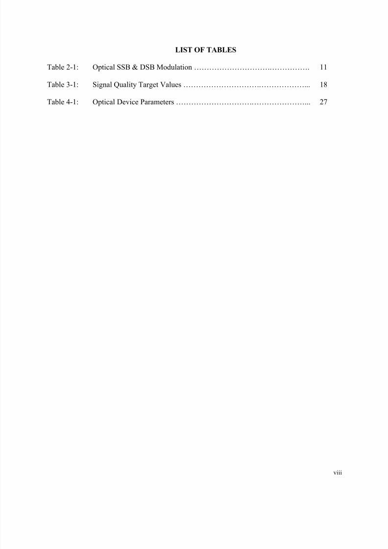
LIST OF TABLES
Table 2-1: Optical SSB & DSB Modulation ………………………………………. 11
Table 3-1: Signal Quality Target Values …………………………………………... 18
Table 4-1: Optical Device Parameters ……………………………………………... 27
8/8/2019 Anthony Leung Thesis
http://slidepdf.com/reader/full/anthony-leung-thesis 10/116
1
CHAPTER 1: INTRODUCTION
1.1 Background
This project studies and examines the transmission performance of SCM Optical
Network to support Broadband Services such as cable TV programs and Broadband Internet
access. After years of anticipation, organizations such as ILECS, CLECS and municipalities are
deploying Fiber to the Home networks in various communities across the states. A Fiber to the
Home (FTTH) network is a residential communications infrastructure where fibers run all the
way to the subscriber premises.
FTTH networks differ from past residential telecommunications infrastructure such as the
telephone and cable TV networks. Those networks were built to support specific applications;
namely, telephone service and cable television. Nowadays, cable modem and DSL technologies
are used to adapt these existing networks to provide broadband Internet access. The current
cable modem and DSL broadband services are sufficient for today’s applications, however, these
technologies will soon face bandwidth limitation challenges to provide next generation
broadband service to customers over coaxial cable and twisted-copper pair wiring. To address
these issues, ATM-PON and Ethernet PON FTTH solutions have been proposed in recent years.
ATM-PON and Ethernet PON are based on the common network architecture, but adopt
different transfer technologies to support integrated services and multiple protocols. ATM-PON
and Ethernet PON both use Time Division Multiple Access (TDMA) based media access control
(MAC) protocol for upstream transmission.
In TDM-based PON, some of the fiber and transceiver-in-feeder networks are shared by
end-users, and only low-cost, passive power splitters are on the light paths between Central
Office (CO) and end users. This enables cost sharing of a transceiver and reduces maintenance
8/8/2019 Anthony Leung Thesis
http://slidepdf.com/reader/full/anthony-leung-thesis 11/116
2
cost significantly. On the other hand, the TDM-based MAC protocols for collision-free
upstream transmission are rather complicated, so the future upgrade of TDM-PON could be a
major challenge. Any change in line rate and frame format for upgrade requires a change of
MAC protocol and thereby the equipment in the network. In addition to upstream transmission
protocol issue, transmission clocks of each customer premises are different from one another.
Therefore, reset and synchronization should be done within the overhead period of each
upstream slot, which is a very challenging task especially at high speed. Furthermore, Video
Broadcasting is one of important services that access network must deliver. While cable TV
service providers provide data services via cable modems in addition to broadcast video services,
telephone providers cannot deliver comparable video broadcasting with the current TDM-based
system. Therefore, broadcast video overlay has become one of major driving force for WDM-
based system.
WDM-based network shares many benefits of TDM-based system. In addition, WDM
efficiently exploits the large capacity of optical fiber without much change in infrastructure and
can provide a virtual point-to-point connection to each end-user, which is totally independent of
line rate and frame format.
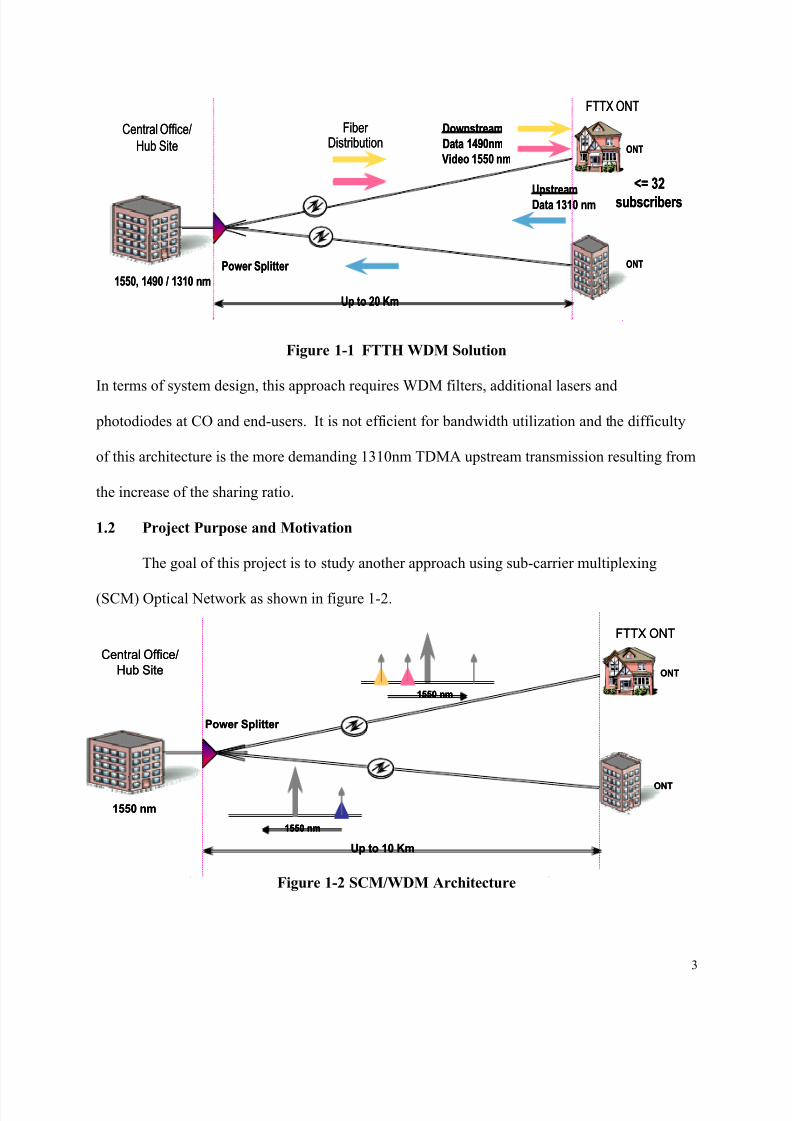
The recent WDM-based FTTH network uses 1550 nm wavelength for CATV video
stream, 1490nm for digital data downstream and 1310nm upstream TDMA as shown in figure
1-1.
8/8/2019 Anthony Leung Thesis
http://slidepdf.com/reader/full/anthony-leung-thesis 12/116
3
Figure 1-1 FTTH WDM Solution
In terms of system design, this approach requires WDM filters, additional lasers and
photodiodes at CO and end-users. It is not efficient for bandwidth utilization and the difficulty
of this architecture is the more demanding 1310nm TDMA upstream transmission resulting from
the increase of the sharing ratio.
1.2 Project Purpose and Motivation
The goal of this project is to study another approach using sub-carrier multiplexing
(SCM) Optical Network as shown in figure 1-2.
Figure 1-2 SCM/WDM Architecture
Power Splitter
<= 32
subscribers
Up to 20 Km
1550, 1490 / 1310 nm
FTTX ONT
Central Office/
Hub Site
ONT
ONT
Fiber
Distribution
Downstream
Data 1490nm
Video 1550 nm
Upstream
Data 1310 nm
Power Splitter
<= 32
subscribers
Up to 20 Km
1550, 1490 / 1310 nm
FTTX ONT
Central Office/
Hub Site
ONT
ONT
Fiber
Distribution
Downstream
Data 1490nm
Video 1550 nm
Upstream
Data 1310 nm
Up to 10 Km
1550 nm
FTTX ONT
Central Office/
Hub Site
ONT
ONT
Power Splitter
1550 nm
1550 nm
Up to 10 Km
1550 nm
FTTX ONT
Central Office/
Hub Site
ONT
ONT
Power Splitter
1550 nm1550 nm
1550 nm1550 nm
8/8/2019 Anthony Leung Thesis
http://slidepdf.com/reader/full/anthony-leung-thesis 13/116
4
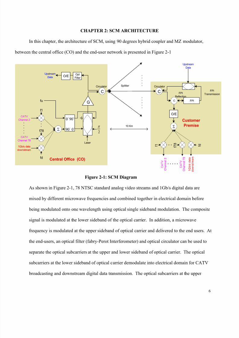
Because of the simplicity and stability of microwave and RF devices, SCM over WDM
can combine different RF channels (analog & digital signals) closely with each other in electrical
domain, and then modulate onto an optical carrier. In this study, 78 NTSC standard analog
video streams and 1Gb/s digital data are mixed by different microwave frequencies and
combined together in the electrical domain before modulating onto one wavelength using optical
single sideband modulation. This composite signal is modulated at the lower sideband of the
optical carrier. In addition, a microwave frequency is modulated at the upper sideband of optical
carrier. At the end-users, an optical filter (fabry-Perot Interferometer) and optical circulator can
be used to separate the optical subcarriers at the upper and lower sideband of optical carrier. The
optical subcarriers at the lower sideband of optical carrier will then demodulate into electrical
domain for CATV broadcasting and downstream digital data transmission. The optical
subcarriers at the upper sideband of optical carrier can be used as an optical source for end-user
upstream digital data transmission.
The goal of this project is to examine the transmission performance of SCM/WDM
network transmitting1Gb/s data and 78 CATV Analog video streams under one wavelength.
Therefore, this project will examine the CATV Carrier-to-Noise Ratio (CNR), the digital data
receiver Q values, the characteristic of fiber nonlinear characteristic as well as the impact of fiber
nonlinear crosstalk to CATV analog and digital transmission performance.
8/8/2019 Anthony Leung Thesis
http://slidepdf.com/reader/full/anthony-leung-thesis 14/116
5
1.3 Project Organization
This project is organized into 6 chapters. In chapter 2, the SCM over WDM
based architecture, using 90 degree hybrid coupler and a Mach-Zender Modulator for optical
single-side band modulation (OSSB), will be presented. In chapter 3, the analytical calculation
of video stream Carrier-to-Noise Ratio (CNR) and Digital Q-Value in optical systems based on a
SCM externally modulated optical link concept model is presented. In chapter 4, a detailed
analysis of Carrier-to-Noise Ratio (CNR) for analog video transmission and digital data Q-value
as well as an overview of the effect of using Dual Parallel linearized external modulator to
suppress third-order nonlinear distortion will be examined. In chapter 5, Stimulated Raman
Scattering (SRS), Cross Phase Modulation (XPM) & Four-wave mixing will be presented and a
detailed analysis of resulting nonlinear crosstalk that impacts on the CATV CNR & digital Q-
Value of SCM/WDM network will be studied. And finally, in chapter 6, the results of the above
analysis are summarized and the problems that need further study are discussed and prospected.
8/8/2019 Anthony Leung Thesis
http://slidepdf.com/reader/full/anthony-leung-thesis 15/116
6
CHAPTER 2: SCM ARCHITECTURE
In this chapter, the architecture of SCM, using 90 degrees hybrid coupler and MZ modulator,
between the central office (CO) and the end-user network is presented in Figure 2-1
C A T V
C h a n n e l 2
C A T V
C h a n n e l 7 8
1 G b / s d a t a
d o w n s t r e a m
C
CATV
Channel 2
CATV
Channel 78
f1
f78
1Gb/s data
downstream
fd
fu
2
π
Σ
o
90
o
90
o
0
o
0
Laser
FPI
O/E
f 7 8
f d
Σ
f 1
Upstream
Data
O/EUpstream
Data
C
Splitter
Opt
Filter
Central Office (CO)
Customer
Premise10 Km
FPI
Reflection
FPI
Transmission
G
CC
Circulator Circulator
Figure 2-1: SCM Diagram
As shown in Figure 2-1, 78 NTSC standard analog video streams and 1Gb/s digital data are
mixed by different microwave frequencies and combined together in electrical domain before
being modulated onto one wavelength using optical single sideband modulation. The composite
signal is modulated at the lower sideband of the optical carrier. In addition, a microwave
frequency is modulated at the upper sideband of optical carrier and delivered to the end users. At
the end-users, an optical filter (fabry-Perot Interferometer) and optical circulator can be used to
separate the optical subcarriers at the upper and lower sideband of optical carrier. The optical
subcarriers at the lower sideband of optical carrier demodulate into electrical domain for CATV
broadcasting and downstream digital data transmission. The optical subcarriers at the upper
8/8/2019 Anthony Leung Thesis
http://slidepdf.com/reader/full/anthony-leung-thesis 16/116
7
sideband of optical carrier are used as an optical source at the end-user for upstream digital data
transmission.
2.1 Subcarrier Modulation
In SCM optical transmission systems, a large variety of modulation scheme become
feasible because all those modulation and demodulation can be done in microwave domain.
2.1.1 Analog AM-VSB Modulation
The standard modulation format for NTSC analog video stream is AM-VSM (Amplitude-
modulation with vestigial sideband modulation). Amplitude modulation with vestigial sideband
(AM-VSB) modulation up converts each video stream on an allocated CATV frequency. The
NTSC standard analog video stream has two major components, picture carrier and audio
subcarrier. The TV luminance and the 3.58 MHz chrominance subcarrier amplitude modulates
an IF carrier (such as 55.25MHz, 61.25MHz, etc), then, an asymmetrically filter is used to filter
portion of the upper sideband of the amplitude modulated signal such that the upper sideband
edge is 1.25MHz above the IF carrier and the lower sideband edge is 4.75MHz below the IF
carrier.
The output expression for VSB-AM is )())cos()(()( t ht t m Act s c ∗⋅⋅= ω , where m(t) is the
video stream input, h (t) is the sideband filter, and )cos( t cω is the microwave frequency. A
separate mixer is needed for each video subcarrier channel at own microwave frequency. A
sinusoidal signal, )cos( t mω , is used to represent video stream input for approximation.
Therefore, the output expression for a 78 VSB-AM modulated signal can be rewritten as
t c At s micii
i
i )cos()(78
1
ω ω −⋅= ∑=
.
8/8/2019 Anthony Leung Thesis
http://slidepdf.com/reader/full/anthony-leung-thesis 17/116
8
2.1.2 Digital Modulation
The Q value of digital data transmission performance of this study is based on the BPSK,
QPSK & ASK (OOK) modulation schemes. The baseband signal is modulated to a subcarrier
frequency by a carrier suppress mixer.
The expression for the output of such a mixer is )cos()()( t t xt y cω ⋅= , where )cos( t cω is
the microwave carrier of downlink digital data and x(t) is the baseband signal. The baseband
signal, x(t), can set as bipolar (+1,-1) for BPSK modulated signal, or unipolar (0, 1) for ASK
modulated signal.
2.2 Optical single-side band Modulation & Mach-Zehnder modulator
After SCM modulation, all subcarriers are combined together by a wideband microwave
power coupler to modulate lightwave from the laser. In this study, external intensity
modulation/direct detection is used to support lightwave analog video and digital data
transmission.
There are two main classes of external modulators available for external intensity
modulation: the Mach-Zehnder (MZ) interferometer and the electroabsorption (EA) modulator.
Compared to EA modulator, the MZ modulator is modulator choice for a vast majority of system
manufacturers because of its lower insertion loss, controlled frequency chirp and its well
behaved on/off characteristics. The MZ device relies on the electro-optic effects to manipulate
the optical phase differently between the two interferometer branches to effect ‘on/off’
switching. Here the switch voltage is commonly referred to as π V and Lithium Niobate (LiNbO3)
is the most common used material.
8/8/2019 Anthony Leung Thesis
http://slidepdf.com/reader/full/anthony-leung-thesis 18/116
9
The conventional MZ modulator consists of waveguides forming two Y junctions in an
electro-optic material with coplanar electrodes over the waveguides. The voltage response of
MZ modulator can be described as [4]
( )[ ] ( )[ ] ( )
−∆⋅=+⋅
⋅= −+−
2cos
4
22
21θ β β ω θ β ω L
L P ee L P
P ain
Lt jl t jainout (2-1)
where P in is the average input optical power, La is the 3-dB waveguide loss at the combiner Y-
junction, ω is the optical carrier frequency, θ is the static bias phase shift between the two arms,
and ∆Βl = ( β 1- β 2)L =π
π
V
t V )(is the applied voltage-induced phase difference between the two
arms.
In order to minimize the impact of fiber chromatic dispersion and to increase the optical
bandwidth efficiency, optical single-side band (OSSB) modulation is used. The OSSB signal
can be generated using MZ modulator. The output of the MZ modulator can be written as [1] &
[5]
[ ] [ ] )cos(coscoscos2
)( θ ω βπ ω ω βπ γπ ω +++++= t t t t At E icico (2-2)
The first and second term of the equation represent the phase modulation of upper and lower arm
of MZ modulator. This two phase modulated optical wave then recombines resulting in
amplitude modulation, where cos(ωit) is the modulating RF signal and cos(ωit+θ) is the phase
shifted modulating RF signal, ω is modulation signal frequency,π
γ V
V dc= is the bias of one arm,
and π βπ π V
V ac= is the optical modulation index.
8/8/2019 Anthony Leung Thesis
http://slidepdf.com/reader/full/anthony-leung-thesis 19/116
10
To obtain optical single side band, the phase difference of the modulating RF signal on
each MZ modulator arm is2
π θ = . In addition, the applied dc Voltage, V dc, drives to one half of
swinging voltage, V Л , to bias the MZ Modulator at the quadrature point to obtain2π phase
difference between two MZ modulator arms. By biasing the MZ Modulator at the quadratue
point, the even order nonlinear distortions are cancelled. The equation in (2-2) can be expanded
in terms of Bessel functions to give
( )
+−−=
+++
++=
t V
V J t t
V
V J
At E
t
V
V t t
V
V
V
V t
At E
icac
ccac
o
iac
ciacdc
co
)cos()(2sincos)(2
)(
)cos(coscoscos
2
)(
10 ω ω π ω ω π
θ ω π ω ω π π ω
π π
π π π (2-3)
The first term is the optical carrier at wavelengthc
c
c
ω
π λ
2= , while the second term is a lower
sideband at the optical frequency ic ω ω + .
Furthermore, in order to double the information capacity transmitting different
information in the two sidebands of the same optical carrier, a 4-port 90-degree RF hybrid is
used along with dual electrode LiNbO3 Mach Zehnder modulator as shown in Figure 2-1.
The 90-degree RF hybrid coupler has two input and two output ports. When signal A
enters port 1, the signal power is divided equally between ports 3 and 4. The output signal at
port 3 will have a –90 degree phase shift and no phase shift at port 4. At the same time, when
signal B enters port 2, the output signal at port 4 will have –90 degree phase shift and no phase
shift at port 3. Nothing is coupled from port 2 to port 1.
When combining RF hybrid coupler and a MZ modulator, several types of optical
modulations can be obtained as summarized in Table 2-1:
8/8/2019 Anthony Leung Thesis
http://slidepdf.com/reader/full/anthony-leung-thesis 20/116
11
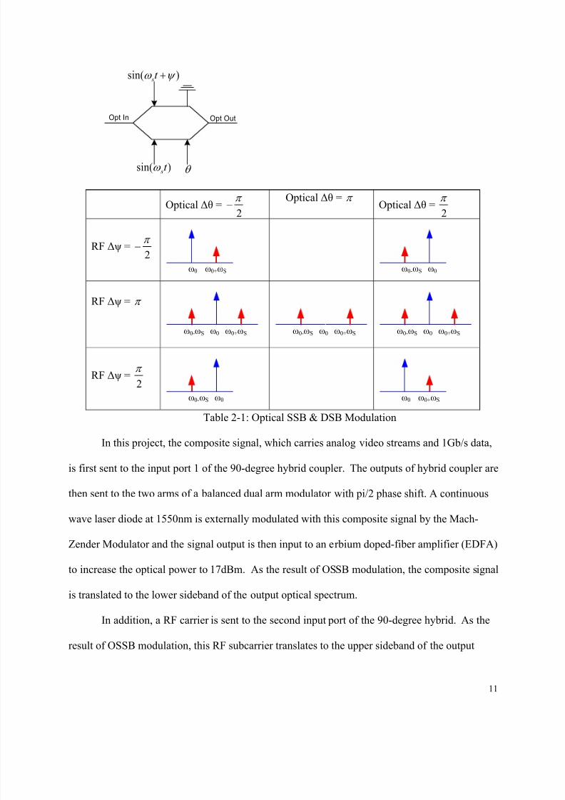
)sin( ψ ω +t s
)sin( t s
ω θ
Opt In Opt Out
Optical ∆θ =2
π −
Optical ∆θ = π Optical ∆θ =
2
π
RF ∆ψ =2
π −
ω0 ω0+ωS ω0-ωS ω0
RF ∆ψ = π
ω0-ωS ω0 ω0+ωS ω0-ωS ω0 ω0+ωS ω0-ωS ω0 ω0+ωS
RF ∆ψ =2
π
ω0-ωS ω0 ω0 ω0+ωS
Table 2-1: Optical SSB & DSB Modulation
In this project, the composite signal, which carries analog video streams and 1Gb/s data,
is first sent to the input port 1 of the 90-degree hybrid coupler. The outputs of hybrid coupler are
then sent to the two arms of a balanced dual arm modulator with pi/2 phase shift. A continuous
wave laser diode at 1550nm is externally modulated with this composite signal by the Mach-
Zender Modulator and the signal output is then input to an erbium doped-fiber amplifier (EDFA)
to increase the optical power to 17dBm. As the result of OSSB modulation, the composite signal
is translated to the lower sideband of the output optical spectrum.
In addition, a RF carrier is sent to the second input port of the 90-degree hybrid. As the
result of OSSB modulation, this RF subcarrier translates to the upper sideband of the output
8/8/2019 Anthony Leung Thesis
http://slidepdf.com/reader/full/anthony-leung-thesis 21/116
12
optical spectrum. This optical subcarrier will be delivered to the end-users as the optical source
for upstream transmission.
The output of MZ modulator can be express as
[ ]
−−
+−
−+−
−=
∑=
t V
A J E
t t xV
A J E
t V
A J E
t t V
A J
E t E
uci
d ci
i
mici
cci
)cos()(
)cos()()(
))(cos()(
)sin()cos()(2
)(
1
1
78
1
1
0
ω ω π
ω ω π
ω ω ω π
ω ω π
π
π
π
π
(2-4)
where the first term is the optical carrier at wavelengthc
c
c
ω
π λ
2= , the second and third terms
represents 78 video signal and digital data at lower sideband of optical carrier, respectively. The
digital data x(t) is (-1,1) for BPSK, 2
1,
2
1− for QPSK, and (0,1) for ASK modulation. The
last term represents the dc optical subcarrier at upper sideband of optical carrier.
2.3 Nonlinear Distortion of Conventional MZ Modulator
The voltage response of MZ modulator in equation (2-1) is
( )
−+=
−∆⋅= θ π
θ β
π V
t V L P L L P P ain
ainout
)(cos1
22cos2 ,
When the MZ modulator is bias at quadrature point, the phase bias between two arms of the
modulator is2
π θ = . The transfer function of the MZ modulator is expressed as a sine wave-like
function of the input voltage. For this reason, signal distortion is always found in a MZ
modulator output. In other words, when multiple carrier frequencies pass through a nonlinear
8/8/2019 Anthony Leung Thesis
http://slidepdf.com/reader/full/anthony-leung-thesis 22/116
13
device such as a conventional MZ modulator, signal products other than the original frequencies
are produced. In analog video transmissions, many channels are allocated close to one another.
As a result, signal distortion in a channel can cause an interference problem with other channels.
Two nonlinear terms generated by MZ modulator are composite second order (CSO) and
composite triple beat (CTB).
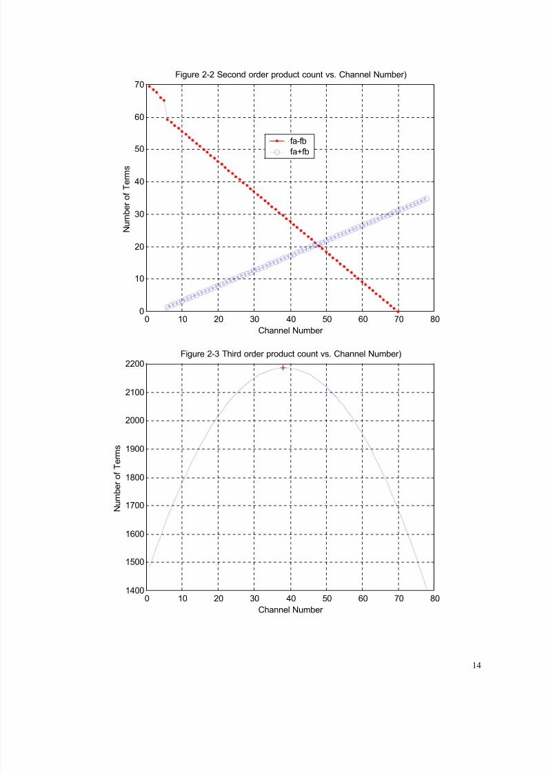
In a multichannel system, the number of CSO terms increase linearly as the number of
channels increase, whereas for CTB terms, it increases as 2 N . Figure 2-2 shows the CSO
( ba f f ± ) Intermodulation product terms for a 78-channel system where the terms ba f f − are
clearly seen to be dominant at the lower end of the multichannel spectrum while at the upper
edge the type ba f f + that dominates. In this case, the number of second-order IM products that
fall right on the first CATV channel is N CSO = 69.
Figure 2-3 shows the CTB ( cba f f f ±± ) Intermodulation product terms for a 78-channel
system where the maximum value of CTB occurs at the centers of the channel groups and where
the number of third-order IM products that fall right on the channel number 38 is N CTB=2185.
8/8/2019 Anthony Leung Thesis
http://slidepdf.com/reader/full/anthony-leung-thesis 23/116
14
0 10 20 30 40 50 60 70 800
10
20
30
40
50
60
70Figure 2-2 Second order product count vs. Channel Number)
Channel Number
N u m b e r o f T e r m s
fa-fb
fa+fb
0 10 20 30 40 50 60 70 801400
1500
1600
1700
1800
1900
2000
2100
2200Figure 2-3 Third order product count vs. Channel Number)
Channel Number
N u m b e r o f T e r m s
8/8/2019 Anthony Leung Thesis
http://slidepdf.com/reader/full/anthony-leung-thesis 24/116
15
In general, second and other high even-order distortions of the MZ modulators can be
eliminated by optimization of the driving bias point at quadrature point. Reference [4]
demonstrates CSO products can be cancelled by setting the dc applied voltage V dc equal to
...),2,1,0(, ±±=mmV π on a dual outputs BBI modulator.
In this project, a conventional MZ modulator with a single output is used and the
derivation of composite second order (CSO) and composite triple beat (CTB) is detailed in
Appendix 2. The power ratio of composite second order (CSO) to carrier is:
2
2
1
01
2
0
2
1
)sin(
)cos(
)]()[(2
)]([)]([2
dc
dc
CSO N
N
V V
V V
N
V
A J
V
A J
V
A J
V
A J
C
CSO
π
π
π π
π π π
π
π π
π π
⋅
= −
−
(2-5)
This formula clearly shows that when the applied dc Voltage is equal to
...),2
3,
2
1(, ±±=mmV π , the CSO distortion is cancelled out. In other words, by setting the
applied dc Voltage equal to
2
π V , all even-order distortion are cancelled and the bias phase shift
between the two arms of modulator is2
π . The power ratio of composite triple beat (CTB) to
carrier is:
2
2
1
01
3
0
3
1
)sin(
)sin(
)]()[(2
)]([)]([2
dc
dc
CTB N
N
V
V
V V
N
V
A J
V
A J
V
A J
V
A J
C
CTB
π
π
π π
π π
π
π
π π
π π
⋅
=−
−
(2-6)
8/8/2019 Anthony Leung Thesis
http://slidepdf.com/reader/full/anthony-leung-thesis 25/116
16
When the optical modulation index isπ
π χ
V
A= << 1, we can approximate 1)(0 = χ J [4] and
2)(1
χ χ = J [4] and equation (2-6) can be simplified as CTB N
x
C
CTB⋅
=
4
2, where N CTB is the
product count of third-order intermodulations in a particular channel.
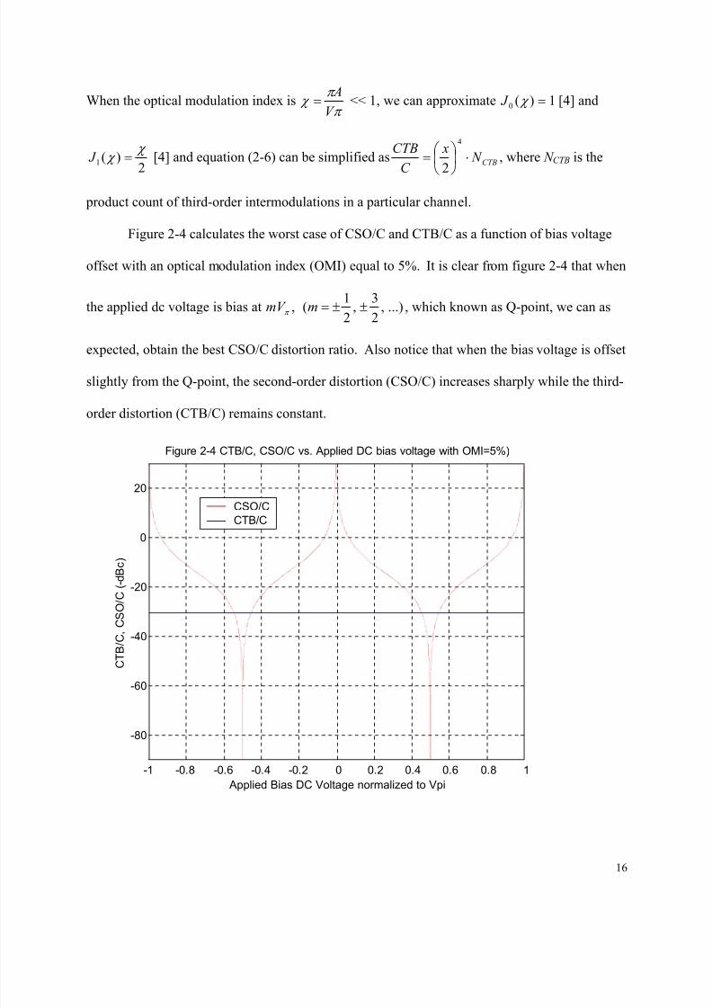
Figure 2-4 calculates the worst case of CSO/C and CTB/C as a function of bias voltage
offset with an optical modulation index (OMI) equal to 5%. It is clear from figure 2-4 that when
the applied dc voltage is bias at ...),2
3,
2
1(, ±±=mmV π , which known as Q-point, we can as
expected, obtain the best CSO/C distortion ratio. Also notice that when the bias voltage is offset
slightly from the Q-point, the second-order distortion (CSO/C) increases sharply while the third-
order distortion (CTB/C) remains constant.
-1 -0.8 -0.6 -0.4 -0.2 0 0.2 0.4 0.6 0.8 1
-80
-60
-40
-20
0
20
Figure 2-4 CTB/C, CSO/C vs. Applied DC bias voltage with OMI=5%)
Applied Bias DC Voltage normalized to Vpi
C T B / C , C S O / C ( - d B c )
CSO/C
CTB/C
8/8/2019 Anthony Leung Thesis
http://slidepdf.com/reader/full/anthony-leung-thesis 26/116
17
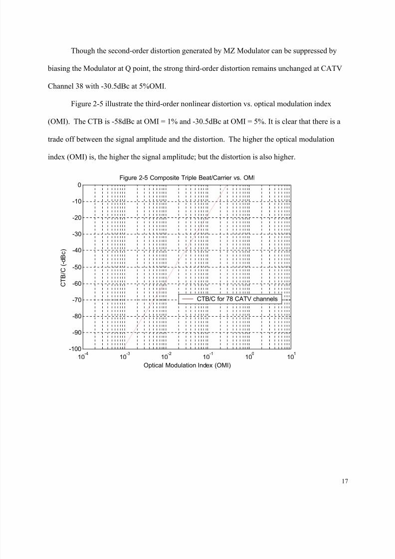
Though the second-order distortion generated by MZ Modulator can be suppressed by
biasing the Modulator at Q point, the strong third-order distortion remains unchanged at CATV
Channel 38 with -30.5dBc at 5%OMI.
Figure 2-5 illustrate the third-order nonlinear distortion vs. optical modulation index
(OMI). The CTB is -58dBc at OMI = 1% and -30.5dBc at OMI = 5%. It is clear that there is a
trade off between the signal amplitude and the distortion. The higher the optical modulation
index (OMI) is, the higher the signal amplitude; but the distortion is also higher.
10-4
10-3
10-2
10-1
100
101
-100
-90
-80
-70
-60
-50
-40
-30
-20
-10
0Figure 2-5 Composite Triple Beat/Carrier vs. OMI
Optical Modulation Index (OMI)
C T B / C ( - d B c )
CTB/C for 78 CATV channels
8/8/2019 Anthony Leung Thesis
http://slidepdf.com/reader/full/anthony-leung-thesis 27/116
18
CHAPTER 3: OPTICAL LINK MODEL FOR CNR AND Q-VALUE CALCULATION
3.1 Analog and Digital Optical Link Model
In analyzing the performance of analog systems, one usually calculates the Carrier-to-
Noise Ratio (CNR) which is expressed as the ratio of the signal power to the total noise power.
In analyzing the performance of digital system, one usually calculates the Bit Error Rate (BER),
or Q-Value.
In order to guarantee a good CNR value, the receiver should have low intrinsic noise and
the detectable signal power should be sufficiently high to dominate this noise power. Other
noise contributions are PIN-receiver shot noise, laser RIN noise, signal-ASE noise generated by
the EDFA booster amplifier, laser clipping, as well as the composite triple beat (CTB) nonlinear
whose distortions can seriously degrade transmission performance.
The FCC requires CNR > 43 dB and distortions such as CSO & CTB > 51dBc under
FCC specification Section 76.605(a). Most systems are design for approximately 48dB CNR at
the end-of-line to account for house amps and bigger TV screens.
The typical digital data specifications requires the BER be 1e-9 or Q value = 6 or better.
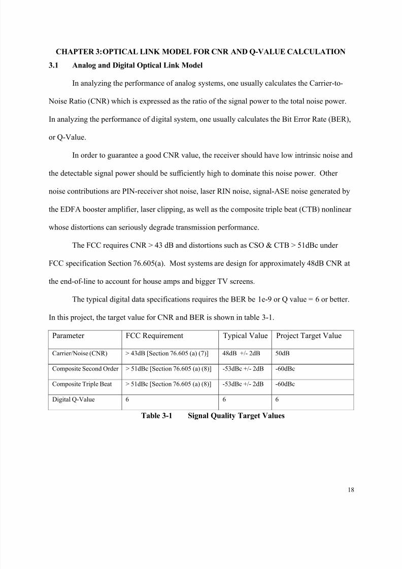
In this project, the target value for CNR and BER is shown in table 3-1.
Parameter FCC Requirement Typical Value Project Target Value
Carrier/Noise (CNR) > 43dB [Section 76.605 (a) (7)] 48dB +/- 2dB 50dB
Composite Second Order > 51dBc [Section 76.605 (a) (8)] -53dBc +/- 2dB -60dBc
Composite Triple Beat > 51dBc [Section 76.605 (a) (8)] -53dBc +/- 2dB -60dBc
Digital Q-Value 6 6 6
Table 3-1 Signal Quality Target Values
8/8/2019 Anthony Leung Thesis
http://slidepdf.com/reader/full/anthony-leung-thesis 28/116
19
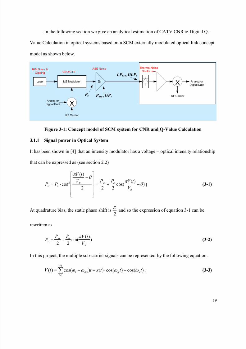
In the following section we give an analytical estimation of CATV CNR & Digital Q-
Value Calculation in optical systems based on a SCM externally modulated optical link concept
model as shown below.
G
ASE Noise
Analog or Digital Data
RF Carrier
Χ
Thermal Noise
Shot Noise
Laser MZ Modulator
Analog or
Digital Data
RF Carrier
Χ
RIN Noise &
Clipping CSO/CTB
P s P ase ,GP s
LP ase ,GLP s
Figure 3-1: Concept model of SCM system for CNR and Q-Value Calculation
3.1.1 Signal power in Optical System
It has been shown in [4] that an intensity modulator has a voltage – optical intensity relationship
that can be expressed as (see section 2.2)
))(cos(222
)(
cos2 θ π
θ π
π
π −+=
−
⋅= V t V P P V
t V
P P ooo s ] (3-1)
At quadrature bias, the static phase shift is2
π and so the expression of equation 3-1 can be
rewritten as
))(
sin(
22 π
π
V
t V P P P oo
s += (3-2)
In this project, the multiple sub-carrier signals can be represented by the following equation:
∑=
+⋅+−=78
1
)cos()cos()()cos()(i
ud imi t t t xt t V ω ω ω ω , (3-3)
8/8/2019 Anthony Leung Thesis
http://slidepdf.com/reader/full/anthony-leung-thesis 29/116
20
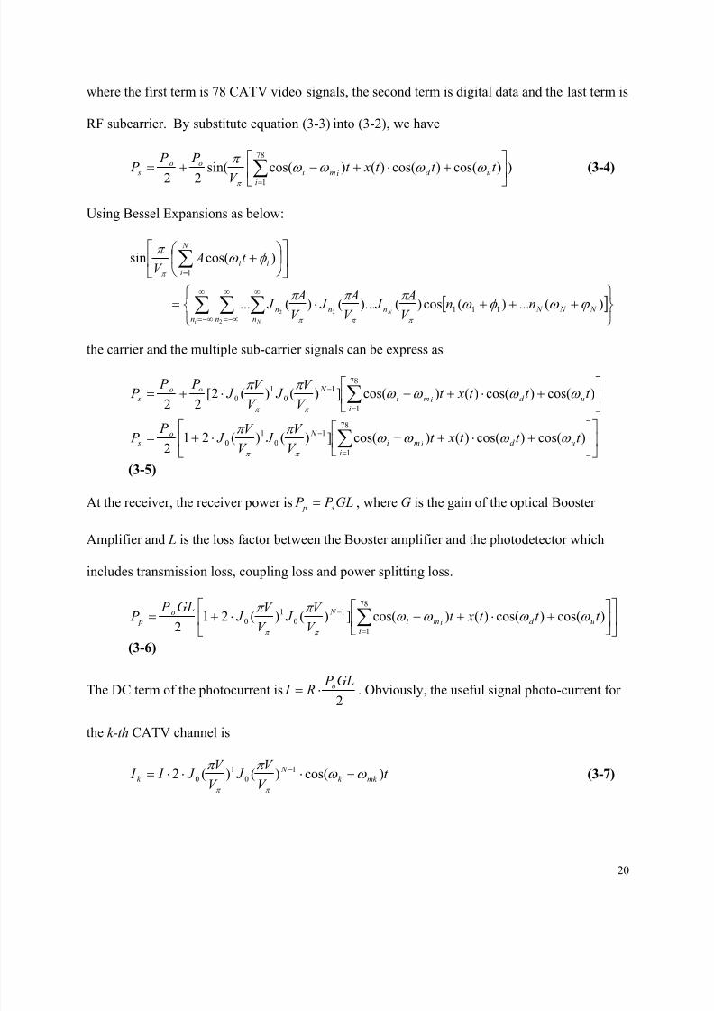
where the first term is 78 CATV video signals, the second term is digital data and the last term is
RF subcarrier. By substitute equation (3-3) into (3-2), we have
))cos()cos()()cos(sin(22
78
1
+⋅+−+=
∑=i
ud i
mioo
s t t t xt V
P P P ω ω ω ω
π
π
(3-4)
Using Bessel Expansions as below:
[ ]
+++⋅=
+
∑ ∑ ∑
∑
∞
−∞=
∞
−∞=
∞
=
i N
N
n n n
N N N nnn
N
i
ii
nnV
A J
V
A J
V
A J
t AV
2
22)(...)(cos)()...()(...
)cos(sin
111
1
ϕ ω φ ω π π π
φ ω π
π π π
π
the carrier and the multiple sub-carrier signals can be express as
+⋅+−⋅+=
+⋅+−⋅+=
∑
∑
=
−
=
−
78
1
1
0
1
0
78
1
1
0
1
0
)cos()cos()()cos(])()(212
)cos()cos()()cos(])()(2[22
i
ud imi
N o s
i
ud imi
N oo s
t t t xt V
V J
V
V J
P P
t t t xt V
V J
V
V J
P P P
ω ω ω ω π π
ω ω ω ω π π
π π
π π
(3-5)
At the receiver, the receiver power is GL P P s p = , where G is the gain of the optical Booster
Amplifier and L is the loss factor between the Booster amplifier and the photodetector which
includes transmission loss, coupling loss and power splitting loss.
+⋅+−⋅+= ∑
=
−78
1
1
0
1
0 )cos()cos()()cos(])()(212 i
ud imi
N o p t t t xt
V
V J
V
V J
GL P P ω ω ω ω
π π
π π
(3-6)
The DC term of the photocurrent is2
GL P R I o⋅= . Obviously, the useful signal photo-current for
the k-th CATV channel is
t V
V J
V
V J I I mk k
N
k )cos()()(2 1
0
1
0 ω ω π π
π π
−⋅⋅⋅= − (3-7)
8/8/2019 Anthony Leung Thesis
http://slidepdf.com/reader/full/anthony-leung-thesis 30/116
21
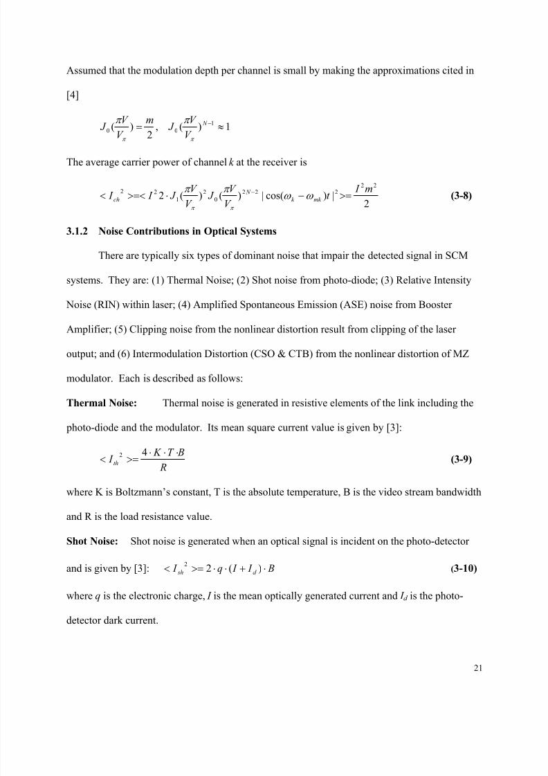
Assumed that the modulation depth per channel is small by making the approximations cited in
[4]
1)(,
2
)( 1
00 ≈= − N
V
V J
m
V
V J
π π
π π
The average carrier power of channel k at the receiver is
2|)cos(|)()(2
22222
0
2
1
22 m I t
V
V J
V
V J I I mk k
N
ch >=−⋅>=<< −ω ω
π π
π π
(3-8)
3.1.2 Noise Contributions in Optical Systems
There are typically six types of dominant noise that impair the detected signal in SCM
systems. They are: (1) Thermal Noise; (2) Shot noise from photo-diode; (3) Relative Intensity
Noise (RIN) within laser; (4) Amplified Spontaneous Emission (ASE) noise from Booster
Amplifier; (5) Clipping noise from the nonlinear distortion result from clipping of the laser
output; and (6) Intermodulation Distortion (CSO & CTB) from the nonlinear distortion of MZ
modulator. Each is described as follows:
Thermal Noise: Thermal noise is generated in resistive elements of the link including the
photo-diode and the modulator. Its mean square current value is given by [3]:
R
BT K I th
⋅⋅⋅>=<
42 (3-9)
where K is Boltzmann’s constant, T is the absolute temperature, B is the video stream bandwidth
and R is the load resistance value.
Shot Noise: Shot noise is generated when an optical signal is incident on the photo-detector
and is given by [3]: B I I q I d sh ⋅+⋅⋅>=< )(22
(3-10)
where q is the electronic charge, I is the mean optically generated current and I d is the photo-
detector dark current.
8/8/2019 Anthony Leung Thesis
http://slidepdf.com/reader/full/anthony-leung-thesis 31/116
22
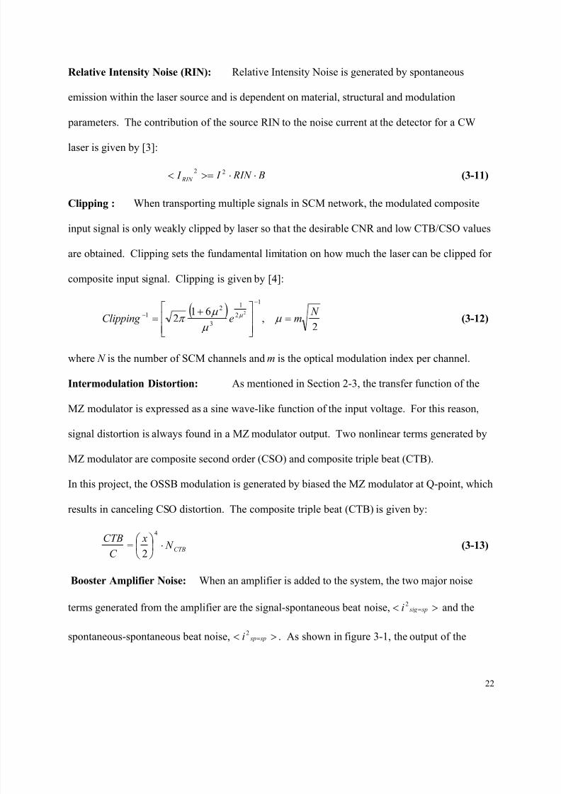
Relative Intensity Noise (RIN): Relative Intensity Noise is generated by spontaneous
emission within the laser source and is dependent on material, structural and modulation
parameters. The contribution of the source RIN to the noise current at the detector for a CW
laser is given by [3]:
B RIN I I RIN ⋅⋅>=< 22 (3-11)
Clipping : When transporting multiple signals in SCM network, the modulated composite
input signal is only weakly clipped by laser so that the desirable CNR and low CTB/CSO values
are obtained. Clipping sets the fundamental limitation on how much the laser can be clipped for
composite input signal. Clipping is given by [4]:
( )2
,61
2
1
2
1
3
21 2 N
meClipping =
+=
−
− µ µ
µ π µ
(3-12)
where N is the number of SCM channels and m is the optical modulation index per channel.
Intermodulation Distortion: As mentioned in Section 2-3, the transfer function of the
MZ modulator is expressed as a sine wave-like function of the input voltage. For this reason,
signal distortion is always found in a MZ modulator output. Two nonlinear terms generated by
MZ modulator are composite second order (CSO) and composite triple beat (CTB).
In this project, the OSSB modulation is generated by biased the MZ modulator at Q-point, which
results in canceling CSO distortion. The composite triple beat (CTB) is given by:
CTB N x
C
CTB⋅
=
4
2
(3-13)
Booster Amplifier Noise: When an amplifier is added to the system, the two major noise
terms generated from the amplifier are the signal-spontaneous beat noise, >< = sp sig i 2 and the
spontaneous-spontaneous beat noise, >< = sp spi 2. As shown in figure 3-1, the output of the
8/8/2019 Anthony Leung Thesis
http://slidepdf.com/reader/full/anthony-leung-thesis 32/116
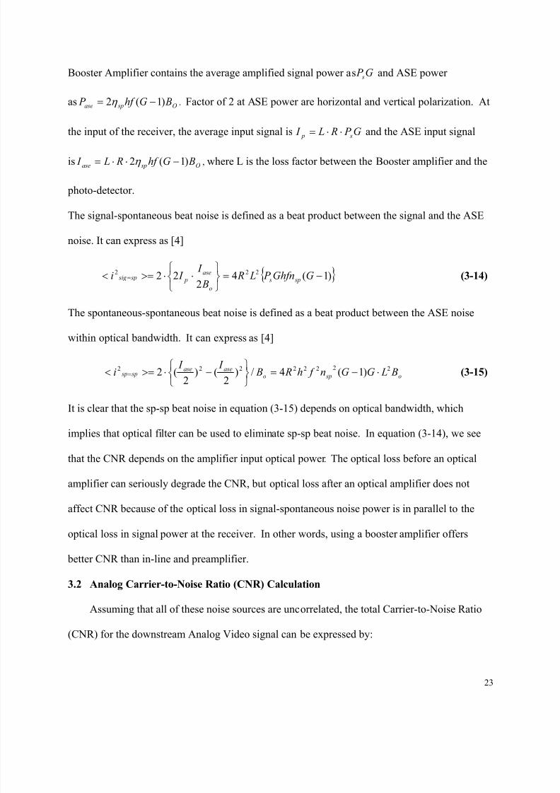
23
Booster Amplifier contains the average amplified signal power as G P s and ASE power
as O spase BGhf P )1(2 −= η . Factor of 2 at ASE power are horizontal and vertical polarization. At
the input of the receiver, the average input signal is G P R L I s p
⋅⋅= and the ASE input signal
is O spase BGhf R L I )1(2 −⋅⋅= η , where L is the loss factor between the Booster amplifier and the
photo-detector.
The signal-spontaneous beat noise is defined as a beat product between the signal and the ASE
noise. It can express as [4]
)1(4222222
−=
⋅⋅>=< = GGhfn P L R B
I
I i sp s
o
ase
p sp sig (3-14)
The spontaneous-spontaneous beat noise is defined as a beat product between the ASE noise
within optical bandwidth. It can express as [4]
o spoasease
sp sp B LGGn f h R B I I
i 22222222 )1(4/)2
()2
(2 ⋅−=
−⋅>=< = (3-15)
It is clear that the sp-sp beat noise in equation (3-15) depends on optical bandwidth, which
implies that optical filter can be used to eliminate sp-sp beat noise. In equation (3-14), we see
that the CNR depends on the amplifier input optical power . The optical loss before an optical
amplifier can seriously degrade the CNR, but optical loss after an optical amplifier does not
affect CNR because of the optical loss in signal-spontaneous noise power is in parallel to the
optical loss in signal power at the receiver. In other words, using a booster amplifier offers
better CNR than in-line and preamplifier.
3.2 Analog Carrier-to-Noise Ratio (CNR) Calculation
Assuming that all of these noise sources are uncorrelated, the total Carrier-to-Noise Ratio
(CNR) for the downstream Analog Video signal can be expressed by:
8/8/2019 Anthony Leung Thesis
http://slidepdf.com/reader/full/anthony-leung-thesis 33/116
24
( )4
1
3
2
1
21
2
1
22
1
22
1
2
22
1
1111111
16[]
612[]
8[]
4[]
8[]
2[
2
−−−−−−
−−−−−−−
⋅+
+++++
⋅=
+++++=
ctb sp
s
p
p p
p
p
total
CTBClipping ASE shot Thermal RIN total
N m
e
RBhfn
I m
BqI
I m
R
KTB
I m
B I RIN
I mCNR
CNRCNRCNRCNRCNRCNRCNR
µ
µ π µ
(3-16)
The total noise becomes the sum of above components, and since some of these components are
signal dependent, the limiting noise is dependent on the received optical power. The first three
noise terms of equation 3-16 can be summarized as followed:
• Thermal noise limited - increasing the optical power transmitted by 1dB will generally
improve the CNR at the receiver by ~ 1dB.
• Shot noise limited - a 1dB increase in optical power will improve the CNR by 0.5dB.
• RIN limited - no benefit to increase optical power.
3.3 Digital Q Value Calculation
Digital communications systems have many advantages over analog systems brought about
by the need to detect the presence or absence of a pulse rather than measure the absolute pulse
shape. Such detection can be made with reasonable accuracy even if the pulses are distorted and
noisy.
The receiver samples the incoming optical pulses at a rate equal to the bit rate of
transmission and a decision, which is usually performed by setting a threshold level, is made as
to whether each pulse corresponds to a “1” or “0” for ASK system or “1” or “-1” for BPSK
system.
The quality of a digital communication system is specified by its BER or Q value. The
BER is specified as the average probability of incorrect bit identification. In general, the higher
8/8/2019 Anthony Leung Thesis
http://slidepdf.com/reader/full/anthony-leung-thesis 34/116
25
the received Q-value, the lower the BER probability will be. The relationship between BER and
Q-value can be express as [3]
QeQerf BER
Q
2
2
21
21
21
−
≈
−= π
,
From equation (3-6), the useful signal photo-current for the digital channel is
)cos()( t t xm I I d p ω ⋅⋅⋅= ,
where x(t) = -1,1 for BPSK, 2
1,
2
1− for QPSK and 1,0 for ASK system
The receiver Q value for BPSK and ASK system can be approximated as
σ 2
)1()1( −−= P P
BPSK
I I Q (3-17)
σ 2
)2
1()
2
1( −−
= P P
QPSK
I I
Q (3-18)
σ 2
)0()1( P P ASK
I I Q
−= (3-19)
where σ is the square root of total noise in an optical receiver, which is the composite of the
signal shot noise, the thermal noise, Laser RIN noise, and ASE Booster amplifier noise.
8/8/2019 Anthony Leung Thesis
http://slidepdf.com/reader/full/anthony-leung-thesis 35/116
26
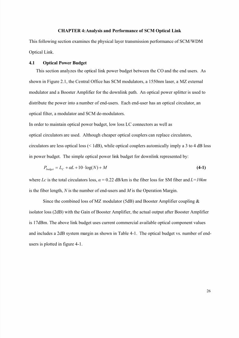
CHAPTER 4: Analysis and Performance of SCM Optical Link
This following section examines the physical layer transmission performance of SCM/WDM
Optical Link.
4.1 Optical Power Budget
This section analyzes the optical link power budget between the CO and the end users. As
shown in Figure 2.1, the Central Office has SCM modulators, a 1550nm laser, a MZ external
modulator and a Booster Amplifier for the downlink path. An optical power splitter is used to
distribute the power into a number of end-users. Each end-user has an optical circulator, an
optical filter, a modulator and SCM de-modulators.
In order to maintain optical power budget, low loss LC connectors as well as
optical circulators are used. Although cheaper optical couplers can replace circulators,
circulators are less optical loss (< 1dB), while optical couplers automically imply a 3 to 4 dB loss
in power budget. The simple optical power link budget for downlink represented by:
M N L L P C budget +⋅++= )log(10α (4-1)
where Lc is the total circulators loss, α = 0.22 dB/km is the fiber loss for SM fiber and L=10km
is the fiber length, N is the number of end-users and M is the Operation Margin.
Since the combined loss of MZ modulator (5dB) and Booster Amplifier coupling &
isolator loss (2dB) with the Gain of Booster Amplifier, the actual output after Booster Amplifier
is 17dBm. The above link budget uses current commercial available optical component values
and includes a 2dB system margin as shown in Table 4-1. The optical budget vs. number of end-
users is plotted in figure 4-1.
8/8/2019 Anthony Leung Thesis
http://slidepdf.com/reader/full/anthony-leung-thesis 36/116
27
Laser
Central Office (CO)Customer Premis
GMZ
PINOpt
Filter
+17 dBm
-5 dBm
-2 dBm couplingand isolator loss
10 Km fiber loss
Splitter Loss
-1 dBm
-1 dBm
PINOptFilter
MZ
-5 dBm
Laser MZ Modulator Booster Amplifier Photodiode
Power = 6, 8 &10dBm Loss=5dB Input Power from -1, 1 & 3dBm Responsivity = 0.8, 0.9A/W
Wavelength = 1550nm Bandwidth = 20GHz Output Power = 17dBm BW = 6MHz (CATV)
RIN=-155, -160dB/Hz Noise Figure = 5dB BW = 0.75GHz (Digital)
nsp = 1.5849 T=300K, Kb=1.38e-23
Coupling and Isolator loss = 2dB Resistance = 1000 ohms
Table 4-1 Optical Device Parameters
0 10 20 30 40 50 606
8
10
12
14
16
18
20
22
24Figure 4-1: Requirement Power Budget (dB) verus the number of End Users
Number of End Users
R e q u i r e d P o w e r B u d g e t ( d B )
8/8/2019 Anthony Leung Thesis
http://slidepdf.com/reader/full/anthony-leung-thesis 37/116
28
RMS modulation index (M)
In general, the signal current at each subcarrier channel is fully dependent upon the
optical modulation index (OMI), “m”, which is a measure of the ratio of the peak modulation of
the individual channel to the average optical power. For a SCM system with 4 subcarrier
channels, the maximum OMI for each channel is 25%.
In common CATV systems, the modulation index (OMI) is twice or more of the
reciprocal of the channel number, i.e., summation of all the modulation indexes will give over
100% modulation. System manufacturers reply upon the fact that the individual channels are not
modulated coherently and the signals add up statistically, seldom reaching 100% OMI, as a
consequence, the laser is operating in its linear region. In this project, the SCM network, which
is composed of 78 video subcarrier channels and 1 digital subcarrier channel, the rms modulation
index (M) is defined as N mM rms = ; where m is the OMI for each channel and N is the total
number of subcarrier channel.
8/8/2019 Anthony Leung Thesis
http://slidepdf.com/reader/full/anthony-leung-thesis 38/116
29
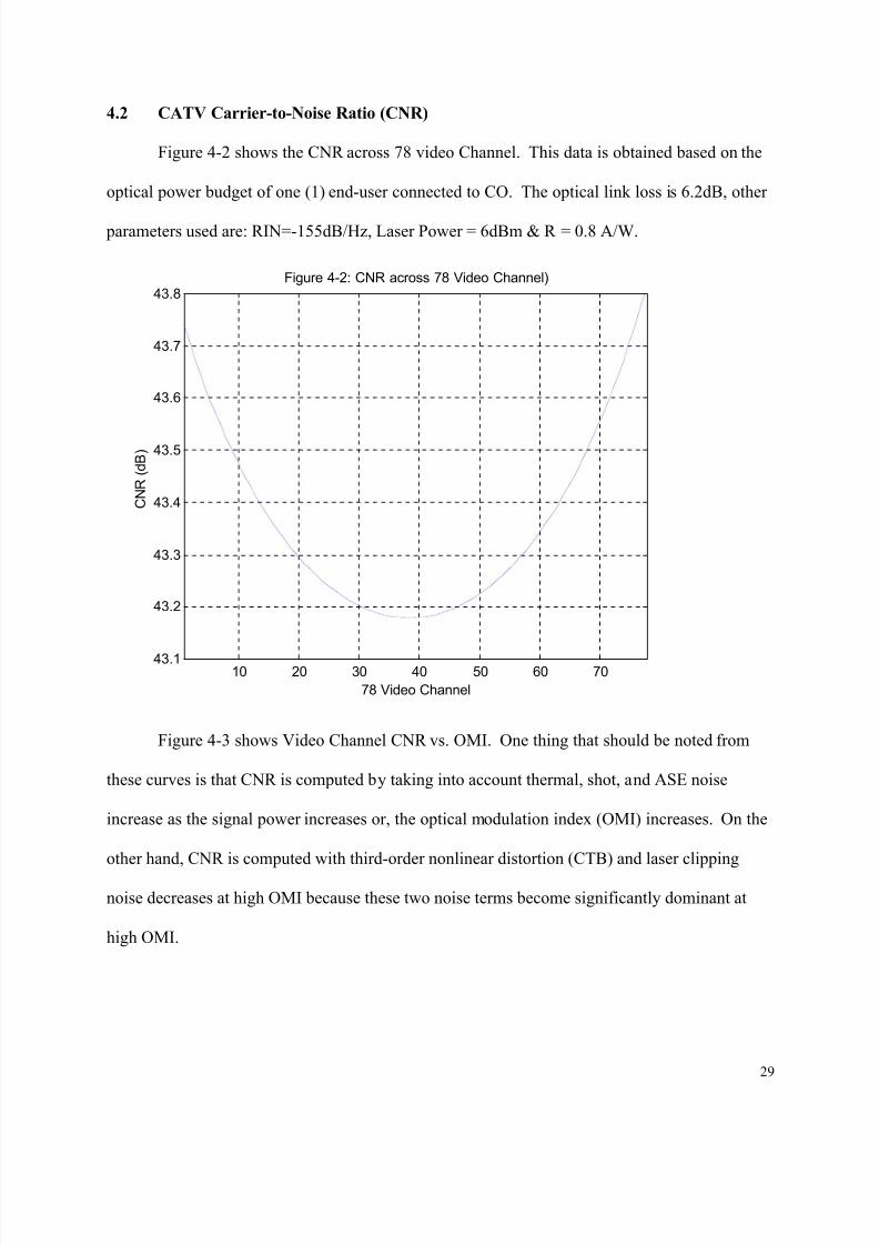
4.2 CATV Carrier-to-Noise Ratio (CNR)
Figure 4-2 shows the CNR across 78 video Channel. This data is obtained based on the
optical power budget of one (1) end-user connected to CO. The optical link loss is 6.2dB, other
parameters used are: RIN=-155dB/Hz, Laser Power = 6dBm & R = 0.8 A/W.
10 20 30 40 50 60 7043.1
43.2
43.3
43.4
43.5
43.6
43.7
43.8Figure 4-2: CNR across 78 Video Channel)
78 Video Channel
C N R ( d B )
Figure 4-3 shows Video Channel CNR vs. OMI. One thing that should be noted from
these curves is that CNR is computed by taking into account thermal, shot, and ASE noise
increase as the signal power increases or, the optical modulation index (OMI) increases. On the
other hand, CNR is computed with third-order nonlinear distortion (CTB) and laser clipping
noise decreases at high OMI because these two noise terms become significantly dominant at
high OMI.
8/8/2019 Anthony Leung Thesis
http://slidepdf.com/reader/full/anthony-leung-thesis 39/116
30
10-4
10-3
10-2
10-1
100
101
0
10
20
30
40
50
60
70
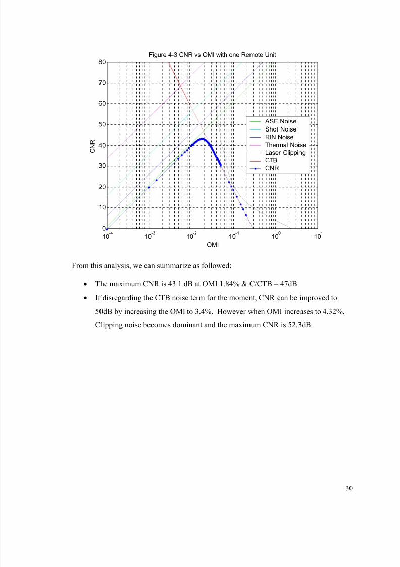
80Figure 4-3 CNR vs OMI with one Remote Unit
OMI
C N R
ASE Noise
Shot Noise
RIN Noise
Thermal Noise
Laser Clipping
CTB
CNR
From this analysis, we can summarize as followed:
• The maximum CNR is 43.1 dB at OMI 1.84% & C/CTB = 47dB
• If disregarding the CTB noise term for the moment, CNR can be improved to
50dB by increasing the OMI to 3.4%. However when OMI increases to 4.32%,
Clipping noise becomes dominant and the maximum CNR is 52.3dB.
8/8/2019 Anthony Leung Thesis
http://slidepdf.com/reader/full/anthony-leung-thesis 40/116
31
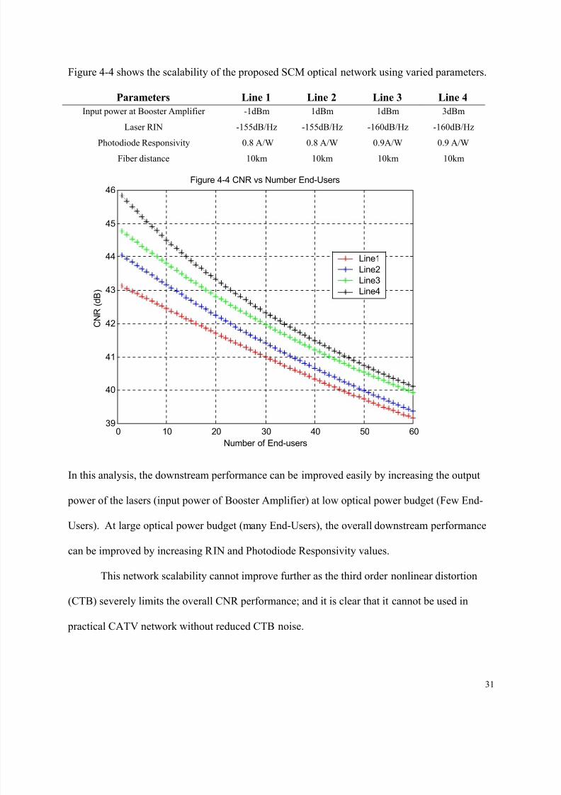
Figure 4-4 shows the scalability of the proposed SCM optical network using varied parameters.
Parameters Line 1 Line 2 Line 3 Line 4
Input power at Booster Amplifier -1dBm 1dBm 1dBm 3dBm
Laser RIN -155dB/Hz -155dB/Hz -160dB/Hz -160dB/Hz
Photodiode Responsivity 0.8 A/W 0.8 A/W 0.9A/W 0.9 A/W
Fiber distance 10km 10km 10km 10km
0 10 20 30 40 50 6039
40
41
42
43
44
45
46Figure 4-4 CNR vs Number End-Users
Number of End-users
C N R ( d B )
Line1
Line2
Line3Line4
In this analysis, the downstream performance can be improved easily by increasing the output
power of the lasers (input power of Booster Amplifier) at low optical power budget (Few End-
Users). At large optical power budget (many End-Users), the overall downstream performance
can be improved by increasing RIN and Photodiode Responsivity values.
This network scalability cannot improve further as the third order nonlinear distortion
(CTB) severely limits the overall CNR performance; and it is clear that it cannot be used in
practical CATV network without reduced CTB noise.
8/8/2019 Anthony Leung Thesis
http://slidepdf.com/reader/full/anthony-leung-thesis 41/116
32
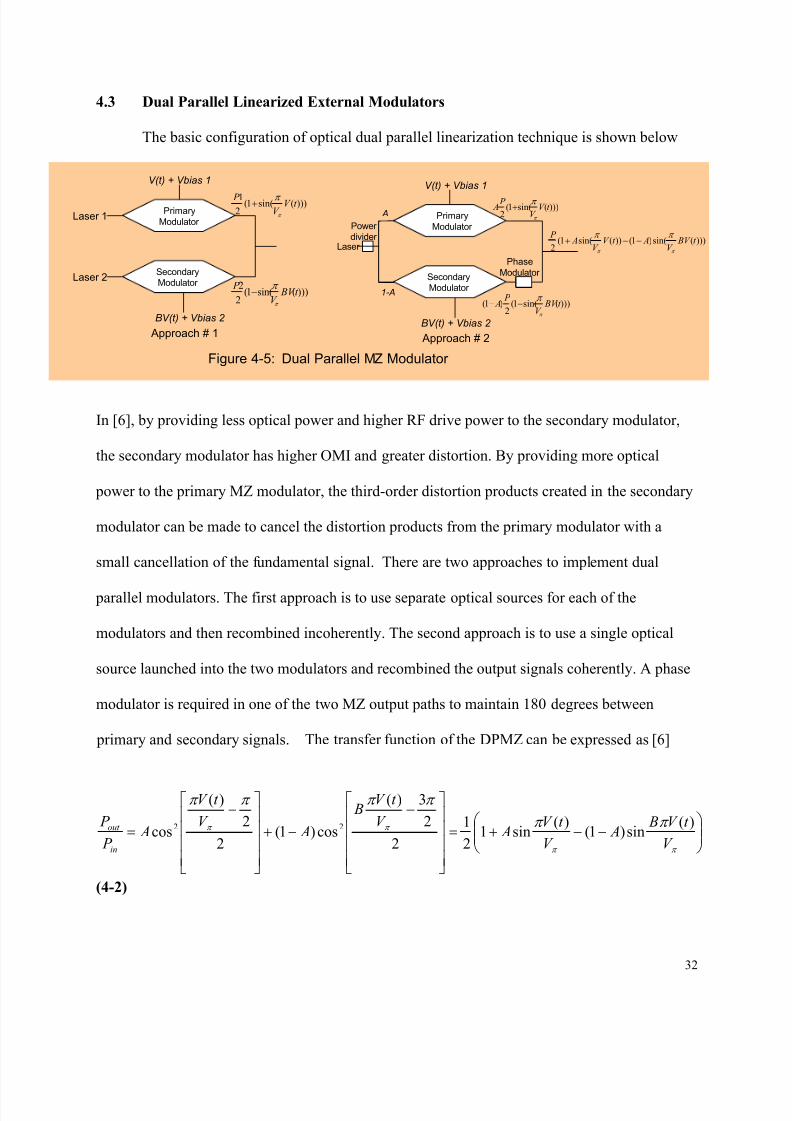
4.3 Dual Parallel Linearized External Modulators
The basic configuration of optical dual parallel linearization technique is shown below
Laser 1
Laser 2
V(t) + Vbias 1
BV(t) + Vbias 2
)))(sin(1(21 t V
V
P
π
π +
)))(sin(1(2
2t BV
V
P
π
π −
Laser
V(t) + Vbias 1
)))(sin(1(2
t V V
P A
π
π +
)))(sin(1(2
)1( t BV V
P A
π
π −−
Approach # 1BV(t) + Vbias 2
A
1-A
Power divider
Primary
Modulator
SecondaryModulator
SecondaryModulator
Primary
Modulator
Phase
Modulator
Approach # 2
)))(sin()1())(sin(1(2
t BV V
At V V
A P
π π
π π −−+
Figure 4-5: Dual Parallel MZ Modulator
In [6], by providing less optical power and higher RF drive power to the secondary modulator,
the secondary modulator has higher OMI and greater distortion. By providing more optical
power to the primary MZ modulator, the third-order distortion products created in the secondary
modulator can be made to cancel the distortion products from the primary modulator with a
small cancellation of the fundamental signal. There are two approaches to implement dual
parallel modulators. The first approach is to use separate optical sources for each of the
modulators and then recombined incoherently. The second approach is to use a single optical
source launched into the two modulators and recombined the output signals coherently. A phase
modulator is required in one of the two MZ output paths to maintain 180 degrees between
primary and secondary signals. The transfer function of the DPMZ can be expressed as [6]
−−+=
−
−+
−
=π π
π π π π
π π π π
V
t V B A
V
t V A
V
t V B
AV
t V
A P
P
in
out )(sin)1(
)(sin1
2
1
2
2
3)(
cos)1(2
2
)(
cos 22
(4-2)
8/8/2019 Anthony Leung Thesis
http://slidepdf.com/reader/full/anthony-leung-thesis 42/116
33
where A is the splitting ratio of the input power divider and B is the ratio of RF drive power.
Assuming V(t) is a multi-sinusoidal signal, using trigonometric identities and Bessel functions,
the amplitude of the fundamental carrier with frequency ωk can be expressed as
1
01
1
01 )()()1()()(−− −−= N N
in V
A B J
V
A B J A
V
A J
V
A AJ
P
P k
π π π π
ω π π π π (4-3)
and the amplitude of the third-order intermodulation component of the frequency ωi+ω j+ωk can
be expressed as
3
0
3
1
3
0
3
1 )()()1()()(−−++
−−= N N
in V
A B J
V
A B J A
V
A J
V
A AJ
P
P k jk
π π π π
ω ω ω π π π π (4-4)
It is easy to show that the third-order intermoduloation product can be cancelled when
3
0
3
1
3
0
3
1
3
0
3
1
)()()()(
)()(
−−
−
+
= N N
N
V
A B J
V
A B J
V
A J
V
A J
V
A B J
V
A B J
A
π π π π
π π
π π π π
π π
(4-5)
The expressions can be simplified by assuming that the modulation depth/channel is small and
by making the approximations [2]
2)(
)(
0
1 m B
Bm J
Bm J = and ,1)4/exp()( 22
0 ≈−≈ N m B Bm J N when m is extremely small
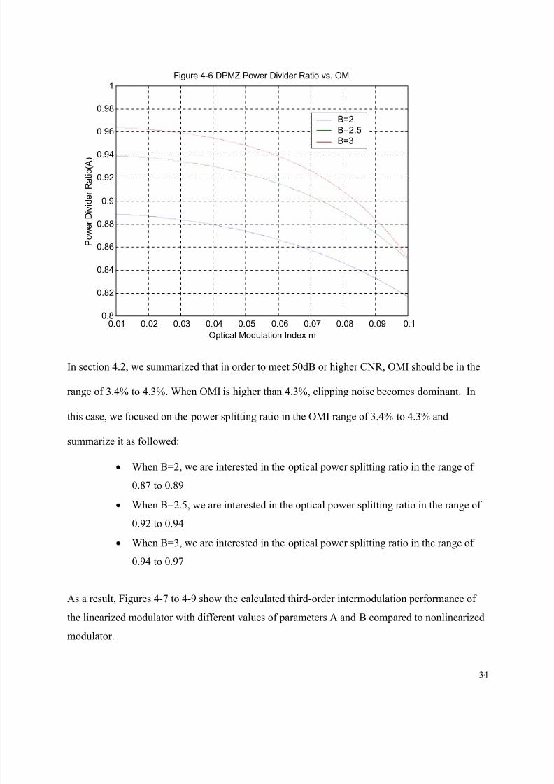
From equation (4-5), we easily find the optimize value of optical power splitting ratio (A) , the
RF drive power (B) and the modulation index (OMI) to minimize third order intermodulation
product. Figure 4-6 shows the variation of the values of optical power splitting ratio required to
attain minimum third order intermodulation product for different values of B and OMI.
8/8/2019 Anthony Leung Thesis
http://slidepdf.com/reader/full/anthony-leung-thesis 43/116
34
0.01 0.02 0.03 0.04 0.05 0.06 0.07 0.08 0.09 0.10.8
0.82
0.84
0.86
0.88
0.9
0.92
0.94
0.96
0.98
1Figure 4-6 DPMZ Power Divider Ratio vs. OMI
Optical Modulation Index m
P o w e r D i v i d e r R a t i o ( A )
B=2
B=2.5
B=3
In section 4.2, we summarized that in order to meet 50dB or higher CNR, OMI should be in the
range of 3.4% to 4.3%. When OMI is higher than 4.3%, clipping noise becomes dominant. In
this case, we focused on the power splitting ratio in the OMI range of 3.4% to 4.3% and
summarize it as followed:
• When B=2, we are interested in the optical power splitting ratio in the range of
0.87 to 0.89
• When B=2.5, we are interested in the optical power splitting ratio in the range of
0.92 to 0.94
• When B=3, we are interested in the optical power splitting ratio in the range of
0.94 to 0.97
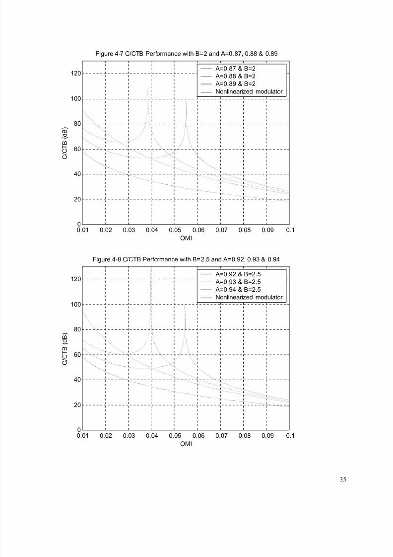
As a result, Figures 4-7 to 4-9 show the calculated third-order intermodulation performance of
the linearized modulator with different values of parameters A and B compared to nonlinearized
modulator.
8/8/2019 Anthony Leung Thesis
http://slidepdf.com/reader/full/anthony-leung-thesis 44/116
35
0.01 0.02 0.03 0.04 0.05 0.06 0.07 0.08 0.09 0.10
20
40
60
80
100
120
Figure 4-7 C/CTB Performance with B=2 and A=0.87, 0.88 & 0.89
OMI
C / C T B ( d B )
A=0.87 & B=2
A=0.88 & B=2
A=0.89 & B=2
Nonlinearized modulator
0.01 0.02 0.03 0.04 0.05 0.06 0.07 0.08 0.09 0.10
20
40
60
80
100
120
Figure 4-8 C/CTB Performance with B=2.5 and A=0.92, 0.93 & 0.94
OMI
C / C T B ( d B )
A=0.92 & B=2.5
A=0.93 & B=2.5
A=0.94 & B=2.5Nonlinearized modulator
8/8/2019 Anthony Leung Thesis
http://slidepdf.com/reader/full/anthony-leung-thesis 45/116
36
0.01 0.02 0.03 0.04 0.05 0.06 0.07 0.08 0.09 0.10
20
40
60
80
100
120
Figure 4-9 C/CTB Performance with B=3 and A=0.94, 0.95, 0.96 & 0.97
OMI
C / C T B ( d B )
A=0.94 & B=3
A=0.95 & B=3
A=0.96 & B=3
A=0.97 & B=3
Nonlinearized modulator
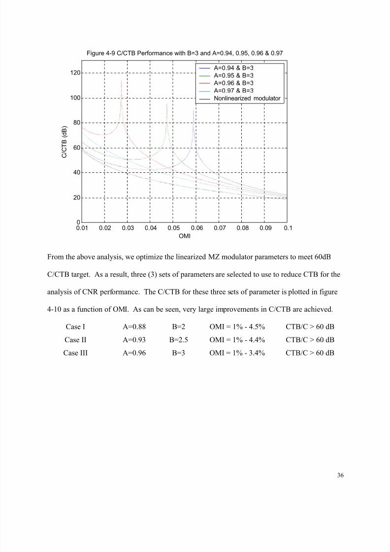
From the above analysis, we optimize the linearized MZ modulator parameters to meet 60dB
C/CTB target. As a result, three (3) sets of parameters are selected to use to reduce CTB for the
analysis of CNR performance. The C/CTB for these three sets of parameter is plotted in figure
4-10 as a function of OMI. As can be seen, very large improvements in C/CTB are achieved.
Case I A=0.88 B=2 OMI = 1% - 4.5% CTB/C > 60 dB
Case II A=0.93 B=2.5 OMI = 1% - 4.4% CTB/C > 60 dB
Case III A=0.96 B=3 OMI = 1% - 3.4% CTB/C > 60 dB
8/8/2019 Anthony Leung Thesis
http://slidepdf.com/reader/full/anthony-leung-thesis 46/116
37
0.01 0.015 0.02 0.025 0.03 0.035 0.04 0.045 0.050
20
40
60
80
100
120
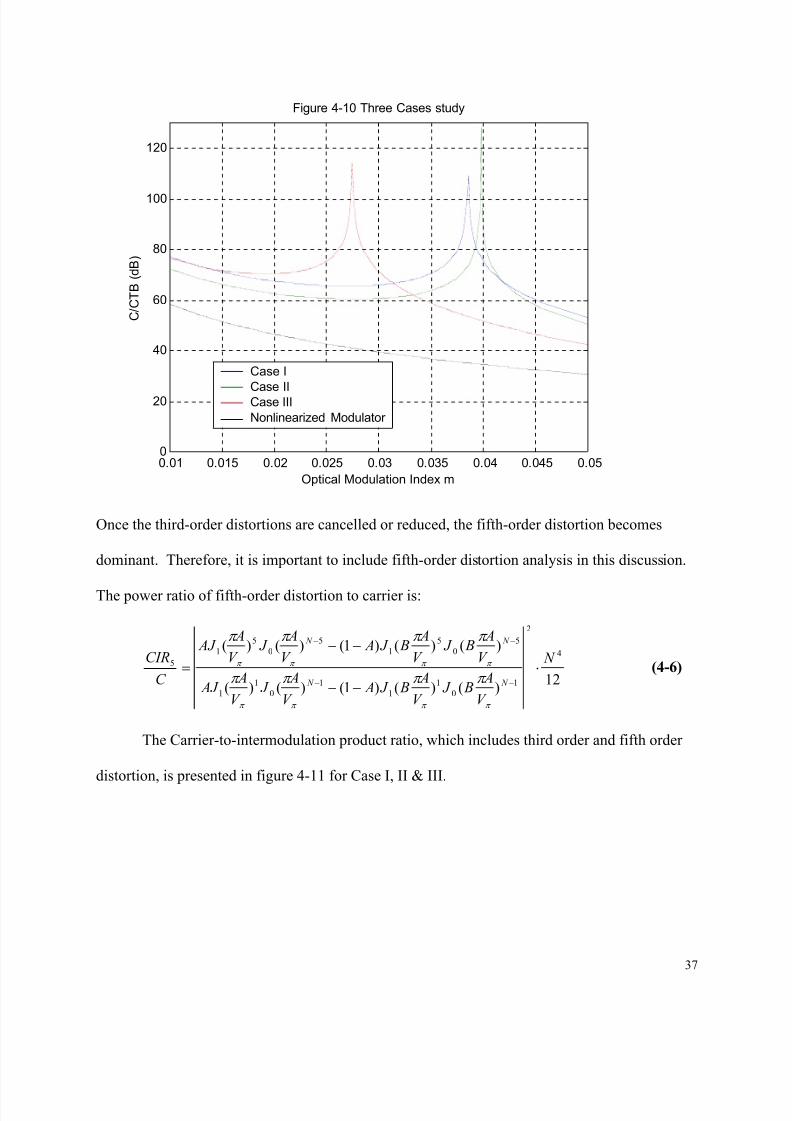
Figure 4-10 Three Cases study
Optical Modulation Index m
C / C T B ( d B )
Case I
Case IICase III
Nonlinearized Modulator
Once the third-order distortions are cancelled or reduced, the fifth-order distortion becomes
dominant. Therefore, it is important to include fifth-order distortion analysis in this discussion.
The power ratio of fifth-order distortion to carrier is:
12)()()1()()(
)()()1()()(4
2
1
0
1
1
1
0
1
1
5
0
5
1
5
0
5
1
5 N
V
A B J
V
A B J A
V
A J
V
A AJ
V
A B J
V
A B J A
V
A J
V
A AJ
C
CIR
N N
N N
⋅
−−
−−
=−−
−−
π π π π
π π π π
π π π π
π π π π
(4-6)
The Carrier-to-intermodulation product ratio, which includes third order and fifth order
distortion, is presented in figure 4-11 for Case I, II & III.
8/8/2019 Anthony Leung Thesis
http://slidepdf.com/reader/full/anthony-leung-thesis 47/116
38
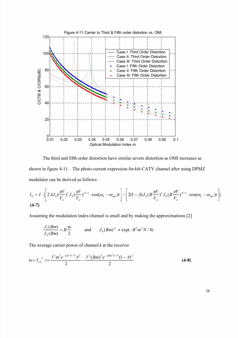
0.01 0.02 0.03 0.04 0.05 0.06 0.07 0.08 0.09 0.10
20
40
60
80
100
120Figure 4-11 Carrier to Third & Fifth order distortion vs. OMI
Optical Modulation Index m
C / C T B & C / C I R 5 ( d B )
Case I: Third Order Distortion
Case II: Third Order Distortion
Case III: Third Order Distortion
Case I: Fifth Order Distortion
Case II: Fifth Order Distortion
Case III: Fifth Order Distortion
The third and fifth order distortion have similar severe distortion as OMI increases as
shown in figure 4-11. The photo-current expression for kth-CATV channel after using DPMZ
modulator can be derived as follows:
)cos()()()1(2)cos()()(2 1
0
1
0
1
0
1
0
−⋅−−
−⋅⋅= −− t
V
V B J
V
V B J At
V
V J
V
V AJ I I mk k
N
mk k
N
k ω ω π π
ω ω π π
π π π π
(4-7)
Assuming the modulation index/channel is small and by making the approximations [2]
2)(
)(
0
1 m B
Bm J
Bm J = and )4/exp()( 22
0 N m B Bm J N −≈
The average carrier power of channel k at the receiver
is2
)1()(
2
24/22224/2222
22
Ae Bm I Aem I I
N Bm N m
ch
−−>=<
−−
(4-8)
8/8/2019 Anthony Leung Thesis
http://slidepdf.com/reader/full/anthony-leung-thesis 48/116
39
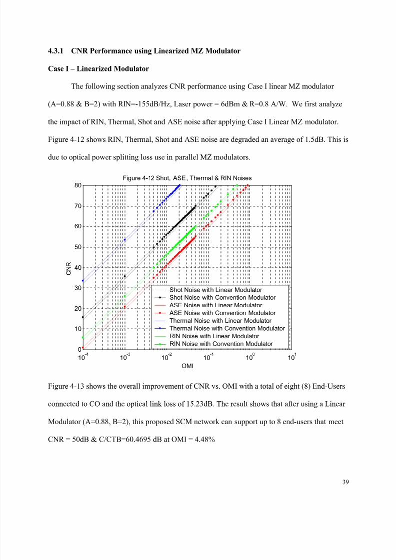
4.3.1 CNR Performance using Linearized MZ Modulator
Case I – Linearized Modulator
The following section analyzes CNR performance using Case I linear MZ modulator
(A=0.88 & B=2) with RIN=-155dB/Hz, Laser power = 6dBm & R=0.8 A/W. We first analyze
the impact of RIN, Thermal, Shot and ASE noise after applying Case I Linear MZ modulator.
Figure 4-12 shows RIN, Thermal, Shot and ASE noise are degraded an average of 1.5dB. This is
due to optical power splitting loss use in parallel MZ modulators.
10-4
10-3
10-2
10-1
100
101
0
10
20
30
40
50
60
70
80Figure 4-12 Shot, ASE, Thermal & RIN Noises
OMI
C N R
Shot Noise with Linear Modulator
Shot Noise with Convention Modulator
ASE Noise with Linear Modulator
ASE Noise with Convention Modulator
Thermal Noise with Linear Modulator
Thermal Noise with Convention Modulator
RIN Noise with Linear Modulator
RIN Noise with Convention Modulator
Figure 4-13 shows the overall improvement of CNR vs. OMI with a total of eight (8) End-Users
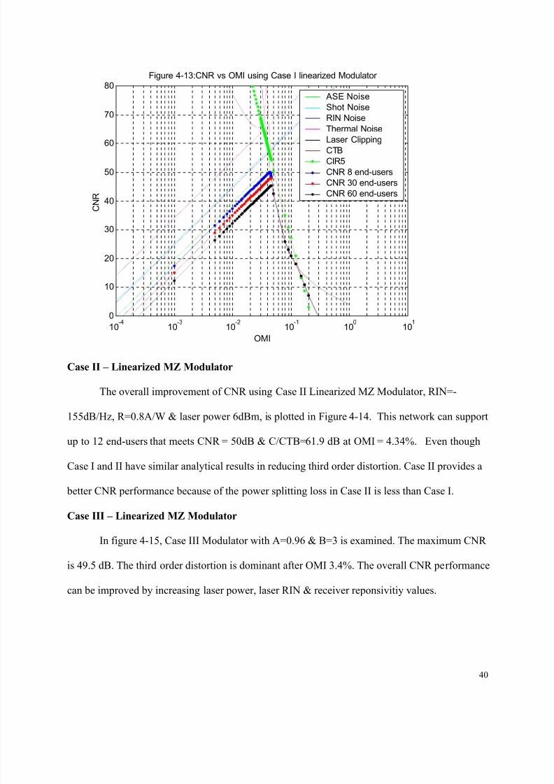
connected to CO and the optical link loss of 15.23dB. The result shows that after using a Linear
Modulator (A=0.88, B=2), this proposed SCM network can support up to 8 end-users that meet
CNR = 50dB & C/CTB=60.4695 dB at OMI = 4.48%
8/8/2019 Anthony Leung Thesis
http://slidepdf.com/reader/full/anthony-leung-thesis 49/116
40
10-4
10-3
10-2
10-1
100
101
0
10
20
30
40
50
60
70
80Figure 4-13:CNR vs OMI using Case I linearized Modulator
OMI
C N R
ASE Noise
Shot Noise
RIN Noise
Thermal Noise
Laser ClippingCTB
CIR5
CNR 8 end-users
CNR 30 end-users
CNR 60 end-users
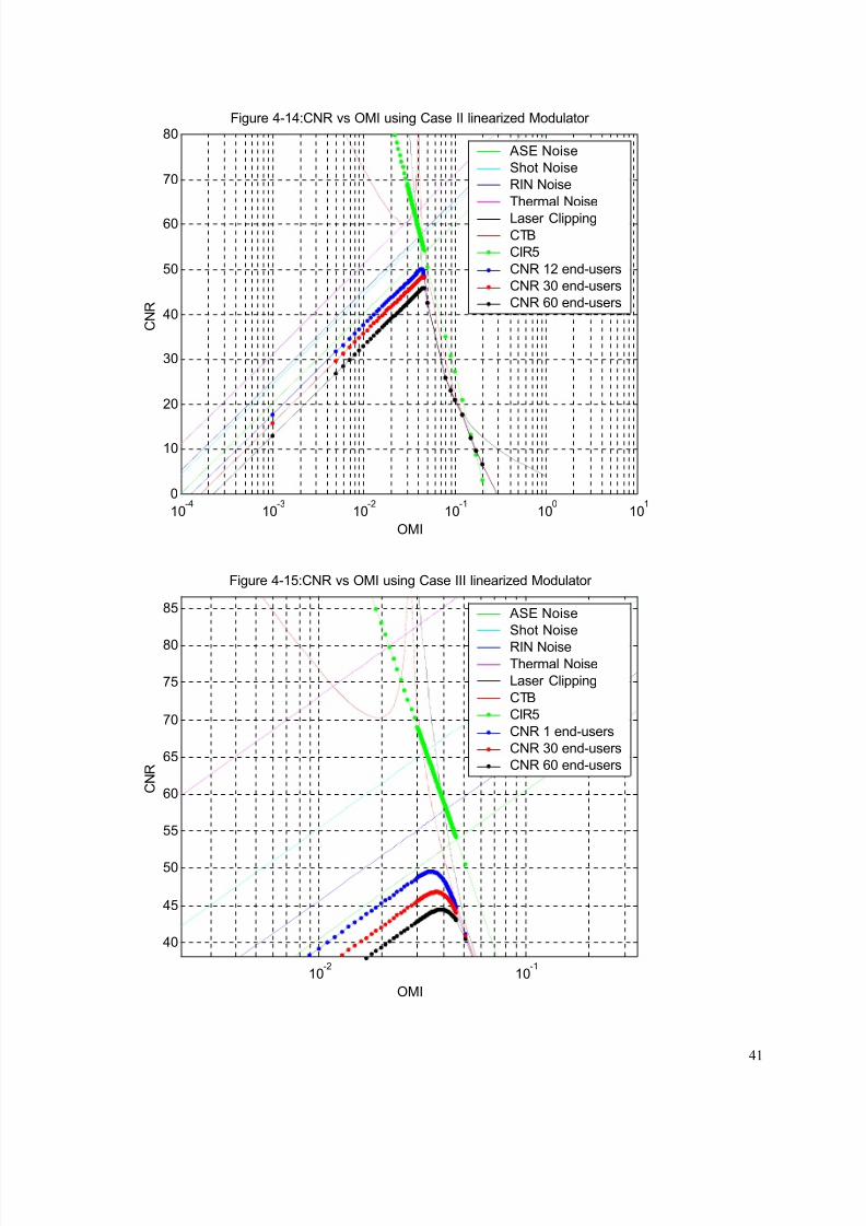
Case II – Linearized MZ Modulator
The overall improvement of CNR using Case II Linearized MZ Modulator, RIN=-
155dB/Hz, R=0.8A/W & laser power 6dBm, is plotted in Figure 4-14. This network can support
up to 12 end-users that meets CNR = 50dB & C/CTB=61.9 dB at OMI = 4.34%. Even though
Case I and II have similar analytical results in reducing third order distortion. Case II provides a
better CNR performance because of the power splitting loss in Case II is less than Case I.
Case III – Linearized MZ Modulator
In figure 4-15, Case III Modulator with A=0.96 & B=3 is examined. The maximum CNR
is 49.5 dB. The third order distortion is dominant after OMI 3.4%. The overall CNR performance
can be improved by increasing laser power, laser RIN & receiver reponsivitiy values.
8/8/2019 Anthony Leung Thesis
http://slidepdf.com/reader/full/anthony-leung-thesis 50/116
41
10-4
10-3
10-2
10-1
100
101
0
10
20
30
40
50
60
70
80Figure 4-14:CNR vs OMI using Case II linearized Modulator
OMI
C N R
ASE Noise
Shot Noise
RIN Noise
Thermal Noise
Laser ClippingCTB
CIR5
CNR 12 end-users
CNR 30 end-users
CNR 60 end-users
10-2
10-1
40
45
50
55
60
65
70
75
80
85
Figure 4-15:CNR vs OMI using Case III linearized Modulator
OMI
C N R
ASE Noise
Shot Noise
RIN NoiseThermal Noise
Laser Clipping
CTB
CIR5
CNR 1 end-users
CNR 30 end-users
CNR 60 end-users
8/8/2019 Anthony Leung Thesis
http://slidepdf.com/reader/full/anthony-leung-thesis 51/116
42
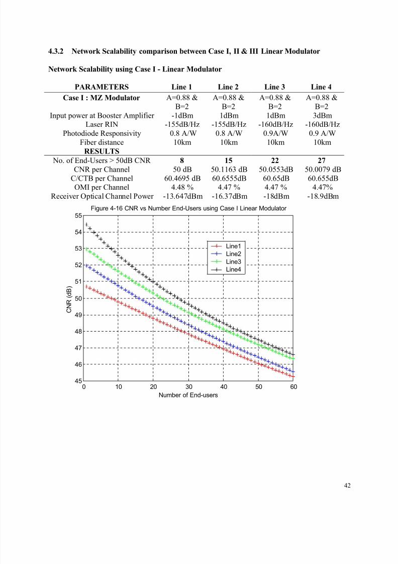
4.3.2 Network Scalability comparison between Case I, II & III Linear Modulator
Network Scalability using Case I - Linear Modulator
PARAMETERS Line 1 Line 2 Line 3 Line 4
Case I : MZ Modulator A=0.88 &B=2
A=0.88 &B=2
A=0.88 &B=2
A=0.88 &B=2
Input power at Booster Amplifier -1dBm 1dBm 1dBm 3dBmLaser RIN -155dB/Hz -155dB/Hz -160dB/Hz -160dB/Hz
Photodiode Responsivity 0.8 A/W 0.8 A/W 0.9A/W 0.9 A/W
Fiber distance 10km 10km 10km 10km
RESULTS
No. of End-Users > 50dB CNR 8 15 22 27
CNR per Channel 50 dB 50.1163 dB 50.0553dB 50.0079 dB
C/CTB per Channel 60.4695 dB 60.6555dB 60.65dB 60.655dBOMI per Channel 4.48 % 4.47 % 4.47 % 4.47%
Receiver Optical Channel Power -13.647dBm -16.37dBm -18dBm -18.9dBm
0 10 20 30 40 50 6045
46
47
48
49
50
51
52
53
54
55Figure 4-16 CNR vs Number End-Users using Case I Linear Modulator
Number of End-users
C N R ( d B )
Line1
Line2
Line3
Line4
8/8/2019 Anthony Leung Thesis
http://slidepdf.com/reader/full/anthony-leung-thesis 52/116
43
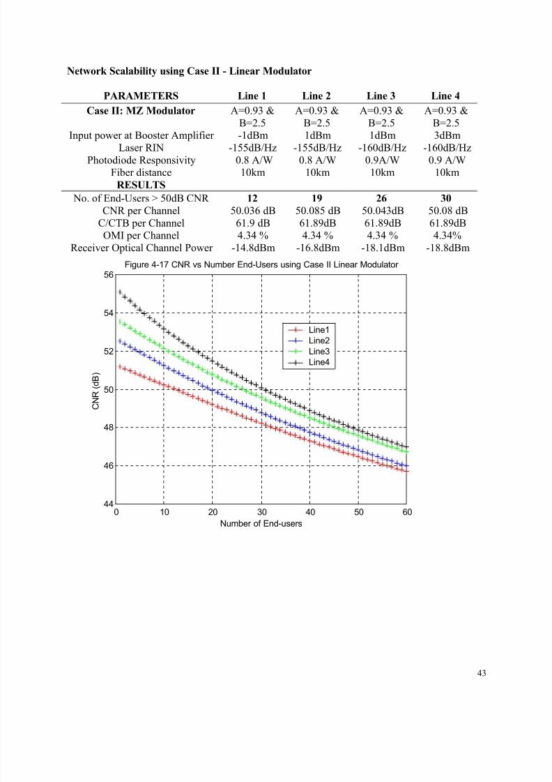
Network Scalability using Case II - Linear Modulator
PARAMETERS Line 1 Line 2 Line 3 Line 4
Case II: MZ Modulator A=0.93 &
B=2.5
A=0.93 &
B=2.5
A=0.93 &
B=2.5
A=0.93 &
B=2.5
Input power at Booster Amplifier -1dBm 1dBm 1dBm 3dBmLaser RIN -155dB/Hz -155dB/Hz -160dB/Hz -160dB/Hz
Photodiode Responsivity 0.8 A/W 0.8 A/W 0.9A/W 0.9 A/WFiber distance 10km 10km 10km 10km
RESULTS
No. of End-Users > 50dB CNR 12 19 26 30
CNR per Channel 50.036 dB 50.085 dB 50.043dB 50.08 dB
C/CTB per Channel 61.9 dB 61.89dB 61.89dB 61.89dBOMI per Channel 4.34 % 4.34 % 4.34 % 4.34%
Receiver Optical Channel Power -14.8dBm -16.8dBm -18.1dBm -18.8dBm
0 10 20 30 40 50 6044
46
48
50
52
54
56
Figure 4-17 CNR vs Number End-Users using Case II Linear Modulator
Number of End-users
C N R ( d B )
Line1
Line2
Line3
Line4
8/8/2019 Anthony Leung Thesis
http://slidepdf.com/reader/full/anthony-leung-thesis 53/116
44
Network Scalability using Case III - Linear Modulator
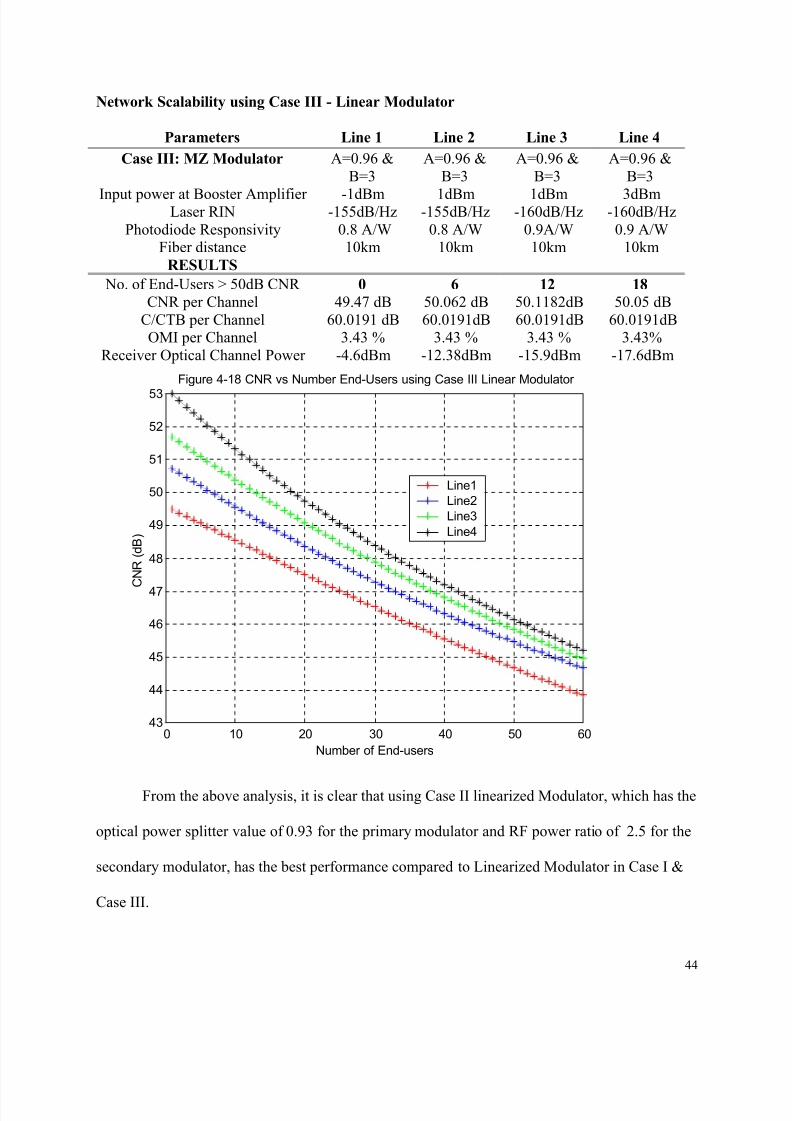
Parameters Line 1 Line 2 Line 3 Line 4
Case III: MZ Modulator A=0.96 &
B=3
A=0.96 &
B=3
A=0.96 &
B=3
A=0.96 &
B=3
Input power at Booster Amplifier -1dBm 1dBm 1dBm 3dBmLaser RIN -155dB/Hz -155dB/Hz -160dB/Hz -160dB/Hz
Photodiode Responsivity 0.8 A/W 0.8 A/W 0.9A/W 0.9 A/WFiber distance 10km 10km 10km 10km
RESULTS
No. of End-Users > 50dB CNR 0 6 12 18
CNR per Channel 49.47 dB 50.062 dB 50.1182dB 50.05 dB
C/CTB per Channel 60.0191 dB 60.0191dB 60.0191dB 60.0191dBOMI per Channel 3.43 % 3.43 % 3.43 % 3.43%
Receiver Optical Channel Power -4.6dBm -12.38dBm -15.9dBm -17.6dBm
0 10 20 30 40 50 6043
44
45
46
47
48
49
50
51
52
53
Figure 4-18 CNR vs Number End-Users using Case III Linear Modulator
Number of End-users
C N R ( d B )
Line1
Line2
Line3
Line4
From the above analysis, it is clear that using Case II linearized Modulator, which has the
optical power splitter value of 0.93 for the primary modulator and RF power ratio of 2.5 for the
secondary modulator, has the best performance compared to Linearized Modulator in Case I &
Case III.
8/8/2019 Anthony Leung Thesis
http://slidepdf.com/reader/full/anthony-leung-thesis 54/116
45
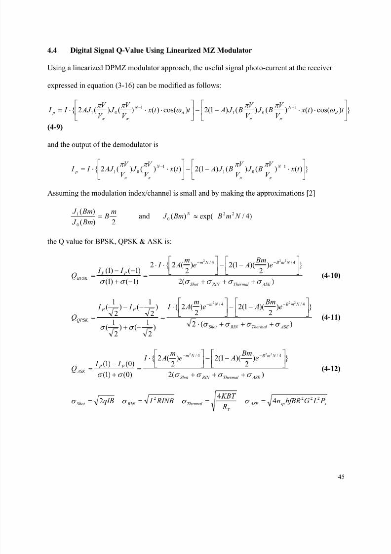
4.4 Digital Signal Q-Value Using Linearized MZ Modulator
Using a linearized DPMZ modulator approach, the useful signal photo-current at the receiver
expressed in equation (3-16) can be modified as follows:
)cos()()()()1(2)cos()()()(2 1
01
1
01
⋅⋅−−
⋅⋅⋅= −− t t x
V
V B J
V
V B J At t x
V
V J
V
V AJ I I d
N
d
N
p ω π π
ω π π
π π π π
(4-9)
and the output of the demodulator is
)()()()1(2)()()(2 1
01
1
01
⋅−−
⋅⋅= −− t x
V
V B J
V
V B J At x
V
V J
V
V AJ I I N N
p
π π π π
π π π π
Assuming the modulation index/channel is small and by making the approximations [2]
2)(
)(
0
1 m B
Bm J
Bm J = and )4/exp()( 22
0 N m B Bm J N −≈
the Q value for BPSK, QPSK & ASK is:
)(2
)2
)(1(2)2
(22
)1()1(
)1()1(
4/4/222
ASE Thermal RIN Shot
N m B N m
P P BPSK
e Bm
Aem
A I I I
Qσ σ σ σ σ σ +++
−−
⋅⋅
=−+
−−=
−−
(4-10)
)(2
)2
)(1(2)2
(2
)2
1()
2
1(
)2
1()
2
1(
4/4/ 222
ASE Thermal RIN Shot
N m B N m
P P
QPSK
e Bm
Aem
A I I I
Qσ σ σ σ σ σ +++⋅
−−
⋅
=
−+
−−
=
−−
(4-11)
)(2
)2
)(1(2)2
(2
)0()1(
)0()1(
4/4/ 222
ASE Thermal RIN Shot
N m B N m
P P ASK
e Bm
Aem
A I I I
Qσ σ σ σ σ σ +++
−−
⋅
=+
−=
−−
(4-12)
s sp ASE
T
Thermal RIN Shot P LGhfBRn R
KBT RINB I qIB 2222
44
2 ==== σ σ σ σ
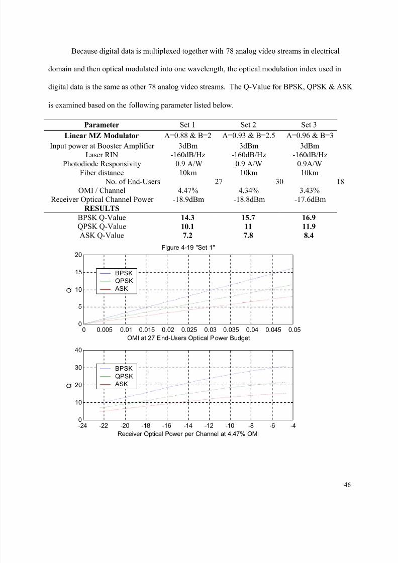
8/8/2019 Anthony Leung Thesis
http://slidepdf.com/reader/full/anthony-leung-thesis 55/116
46
Because digital data is multiplexed together with 78 analog video streams in electrical
domain and then optical modulated into one wavelength, the optical modulation index used in
digital data is the same as other 78 analog video streams. The Q-Value for BPSK, QPSK & ASK
is examined based on the following parameter listed below.
Parameter Set 1 Set 2 Set 3
Linear MZ Modulator A=0.88 & B=2 A=0.93 & B=2.5 A=0.96 & B=3
Input power at Booster Amplifier 3dBm 3dBm 3dBm
Laser RIN -160dB/Hz -160dB/Hz -160dB/Hz
Photodiode Responsivity 0.9 A/W 0.9 A/W 0.9A/W
Fiber distance 10km 10km 10km No. of End-Users 27 30 18
OMI / Channel 4.47% 4.34% 3.43%
Receiver Optical Channel Power -18.9dBm -18.8dBm -17.6dBmRESULTS
BPSK Q-Value 14.3 15.7 16.9
QPSK Q-Value 10.1 11 11.9
ASK Q-Value 7.2 7.8 8.4
0 0.005 0.01 0.015 0.02 0.025 0.03 0.035 0.04 0.045 0.050
5
10
15
20Figure 4-19 "Set 1"
OMI at 27 End-Users Optical Power Budget
Q
BPSK
QPSK
ASK
-24 -22 -20 -18 -16 -14 -12 -10 -8 -6 -40
10
20
30
40
Receiver Optical Power per Channel at 4.47% OMI
Q
BPSK
QPSK
ASK
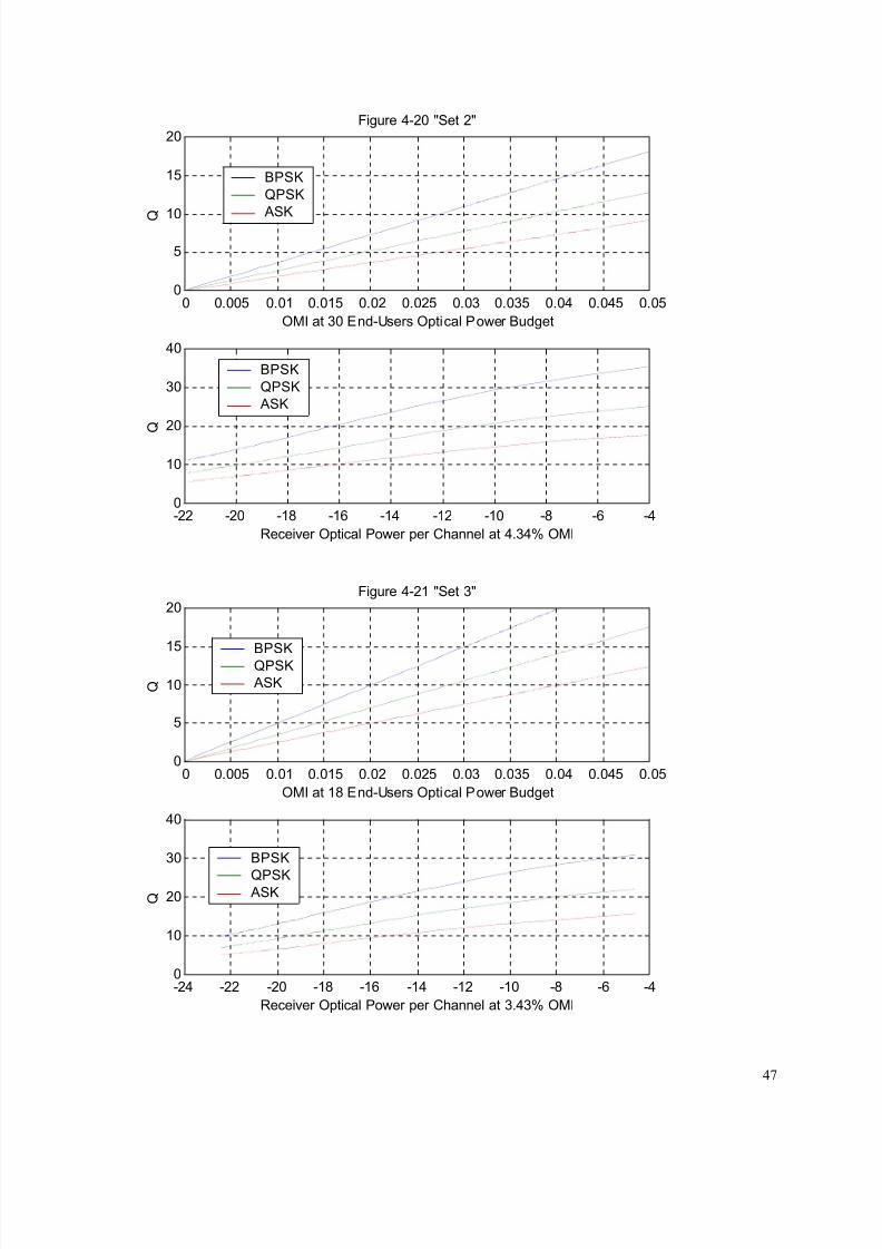
8/8/2019 Anthony Leung Thesis
http://slidepdf.com/reader/full/anthony-leung-thesis 56/116
47
0 0.005 0.01 0.015 0.02 0.025 0.03 0.035 0.04 0.045 0.050
5
10
15
20Figure 4-20 "Set 2"
OMI at 30 End-Users Optical Power Budget
Q
BPSK
QPSK
ASK
-22 -20 -18 -16 -14 -12 -10 -8 -6 -40
10
20
30
40
Receiver Optical Power per Channel at 4.34% OMI
Q
BPSK
QPSK
ASK
0 0.005 0.01 0.015 0.02 0.025 0.03 0.035 0.04 0.045 0.050
5
10
15
20Figure 4-21 "Set 3"
OMI at 18 End-Users Optical Power Budget
Q
BPSK
QPSK
ASK
-24 -22 -20 -18 -16 -14 -12 -10 -8 -6 -40
10
20
30
40
Receiver Optical Power per Channel at 3.43% OMI
Q
BPSK
QPSKASK
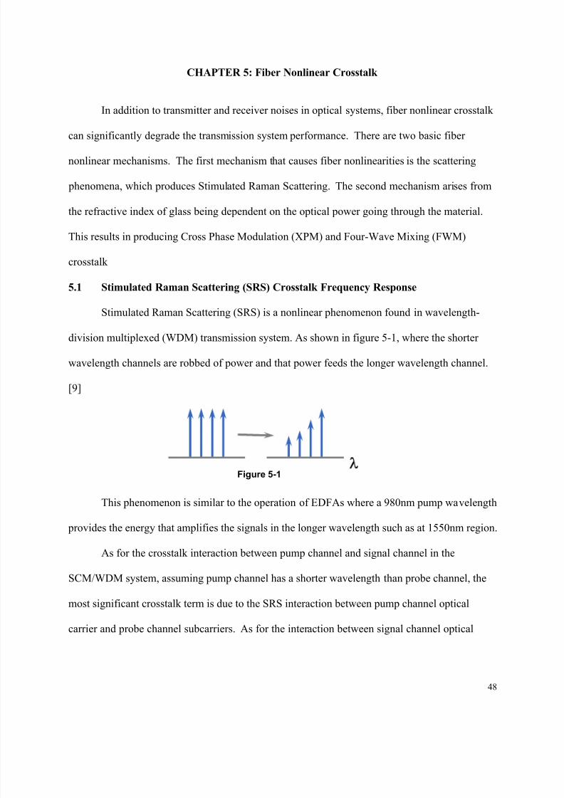
8/8/2019 Anthony Leung Thesis
http://slidepdf.com/reader/full/anthony-leung-thesis 57/116
48
CHAPTER 5: Fiber Nonlinear Crosstalk
In addition to transmitter and receiver noises in optical systems, fiber nonlinear crosstalk
can significantly degrade the transmission system performance. There are two basic fiber
nonlinear mechanisms. The first mechanism that causes fiber nonlinearities is the scattering
phenomena, which produces Stimulated Raman Scattering. The second mechanism arises from
the refractive index of glass being dependent on the optical power going through the material.
This results in producing Cross Phase Modulation (XPM) and Four-Wave Mixing (FWM)
crosstalk
5.1 Stimulated Raman Scattering (SRS) Crosstalk Frequency Response
Stimulated Raman Scattering (SRS) is a nonlinear phenomenon found in wavelength-
division multiplexed (WDM) transmission system. As shown in figure 5-1, where the shorter
wavelength channels are robbed of power and that power feeds the longer wavelength channel.
[9]
This phenomenon is similar to the operation of EDFAs where a 980nm pump wavelength
provides the energy that amplifies the signals in the longer wavelength such as at 1550nm region.
As for the crosstalk interaction between pump channel and signal channel in the
SCM/WDM system, assuming pump channel has a shorter wavelength than probe channel, the
most significant crosstalk term is due to the SRS interaction between pump channel optical
carrier and probe channel subcarriers. As for the interaction between signal channel optical
λFigure 5-1
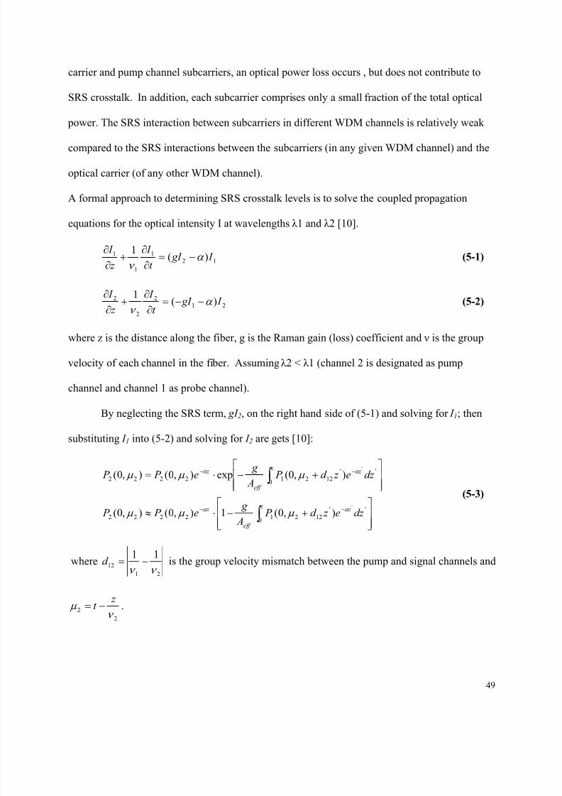
8/8/2019 Anthony Leung Thesis
http://slidepdf.com/reader/full/anthony-leung-thesis 58/116
49
carrier and pump channel subcarriers, an optical power loss occurs , but does not contribute to
SRS crosstalk. In addition, each subcarrier comprises only a small fraction of the total optical
power. The SRS interaction between subcarriers in different WDM channels is relatively weak
compared to the SRS interactions between the subcarriers (in any given WDM channel) and the
optical carrier (of any other WDM channel).
A formal approach to determining SRS crosstalk levels is to solve the coupled propagation
equations for the optical intensity I at wavelengths λ 1 and λ 2 [10].
121
1
1 )(1
I gI t
I
z
I α
ν −=
∂
∂+
∂
∂ (5-1)
212
2
2 )(1
I gI t
I
z
I α
ν −−=
∂
∂+
∂
∂ (5-2)
where z is the distance along the fiber, g is the Raman gain (loss) coefficient and ν is the group
velocity of each channel in the fiber. Assuming λ 2 < λ 1 (channel 2 is designated as pump
channel and channel 1 as probe channel).
By neglecting the SRS term, gI 2, on the right hand side of (5-1) and solving for I 1; then
substituting I 1 into (5-2) and solving for I 2 are gets [10]:
+−⋅≈
+−⋅=
∫
∫
−−
−−
z z
eff
z
z z
eff
z
dz e z d P A
g e P P
dz e z d P A
g e P P
0
''
12212222
0
''
12212222
'
'
),0(1),0(),0(
),0(exp),0(),0(
α α
α α
µ µ µ
µ µ µ
(5-3)
where21
12 11ν ν
−=d is the group velocity mismatch between the pump and signal channels and
2
2ν
µ z
t −= .
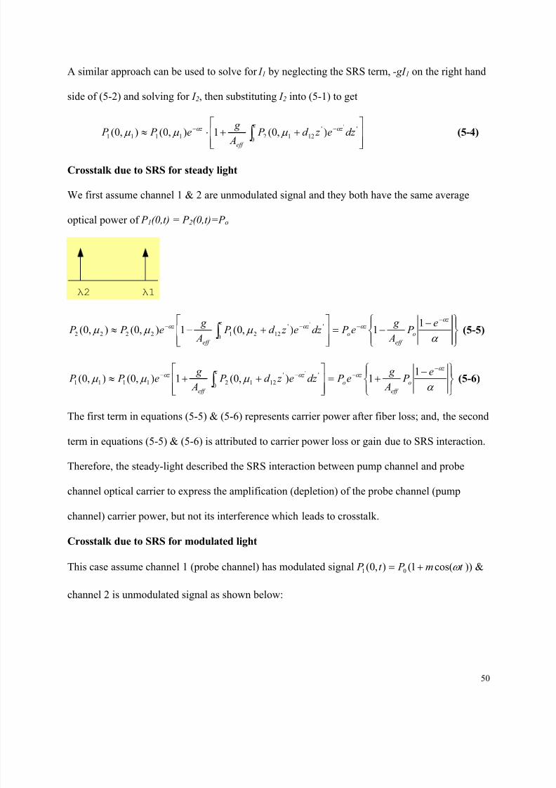
8/8/2019 Anthony Leung Thesis
http://slidepdf.com/reader/full/anthony-leung-thesis 59/116
50
A similar approach can be used to solve for I 1 by neglecting the SRS term, -gI 1 on the right hand
side of (5-2) and solving for I 2, then substituting I 2 into (5-1) to get
++⋅≈
∫
−−z
z
eff
z dz e z d P A
g e P P
0
''
12121111
'
),0(1),0(),0( α α µ µ µ (5-4)
Crosstalk due to SRS for steady light
We first assume channel 1 & 2 are unmodulated signal and they both have the same average
optical power of P 1(0,t) = P 2(0,t)=P o
λ2 λ1
−
−=
+−≈
−−−−
∫ α µ µ µ
α α α α
z
o
eff
z
o
z z
eff
z e P
A
g e P dz e z d P
A
g e P P
11),0(1),0(),0(
0
''
12212222
'
(5-5)
−
+=
++≈
−−−−
∫ α µ µ µ
α α α α
z
o
eff
z
o
z z
eff
z e P
A
g e P dz e z d P
A
g e P P
11),0(1),0(),0(
0
''
12121111
'
(5-6)
The first term in equations (5-5) & (5-6) represents carrier power after fiber loss; and, the second
term in equations (5-5) & (5-6) is attributed to carrier power loss or gain due to SRS interaction.
Therefore, the steady-light described the SRS interaction between pump channel and probe
channel optical carrier to express the amplification (depletion) of the probe channel (pump
channel) carrier power, but not its interference which leads to crosstalk.
Crosstalk due to SRS for modulated light
This case assume channel 1 (probe channel) has modulated signal ))cos(1(),0( 01 t m P t P ω += &
channel 2 is unmodulated signal as shown below:
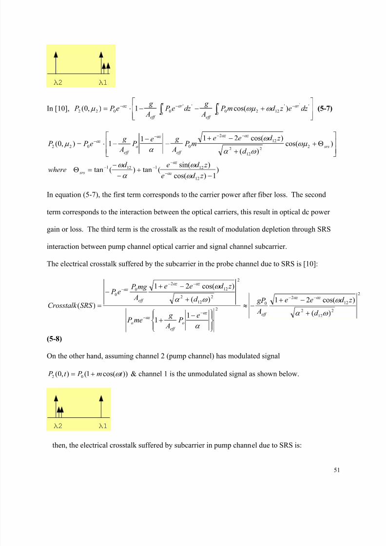
8/8/2019 Anthony Leung Thesis
http://slidepdf.com/reader/full/anthony-leung-thesis 60/116
51
λ2 λ1
In [10],
+−−⋅= ∫ ∫
−−− z z
eff
z z
eff
z dz e z d m P A
g dz e P
A
g e P P
0
''
12200
''
0022
'
)cos(1),0( α α α ω ωµ µ (5-7)
)1)cos(
)sin((tan)(tan
)cos()(
)cos(2111),0(
12
121121
22
12
2
12
2
0022
−+
−
−=Θ
Θ+
+
−+−
−−⋅=
−
−−−
−−−−
z d e
z d ed where
d
z d eem P
A
g e P
A
g e P P
z
z
srs
srs
z z
eff
z
o
eff
z
ω
ω
α
ω
ωµ ω α
ω
α µ
α
α
α α α α
In equation (5-7), the first term corresponds to the carrier power after fiber loss. The second
term corresponds to the interaction between the optical carriers, this result in optical dc power
gain or loss. The third term is the crosstalk as the result of modulation depletion through SRS
interaction between pump channel optical carrier and signal channel subcarrier.
The electrical crosstalk suffered by the subcarrier in the probe channel due to SRS is [10]:
2
2
12
2
12
2
0
2
2
2
12
2
12
2
0
0
)(
)cos(21
11
)(
)cos(21
)(ω α
ω
α
ω α
ω α α
α α
α α
α
d
z d ee
A
gP
e P
A
g me P
d
z d ee A
mg P e P
SRS Crosstalk
z z
eff z
o
eff
z
o
z z
eff
z
+
−+−≈
−
+
+−+−
=−−
−−
−−
−
(5-8)
On the other hand, assuming channel 2 (pump channel) has modulated signal
))cos(1(),0( 02 t m P t P ω += & channel 1 is the unmodulated signal as shown below.
λ2 λ1
then, the electrical crosstalk suffered by subcarrier in pump channel due to SRS is:
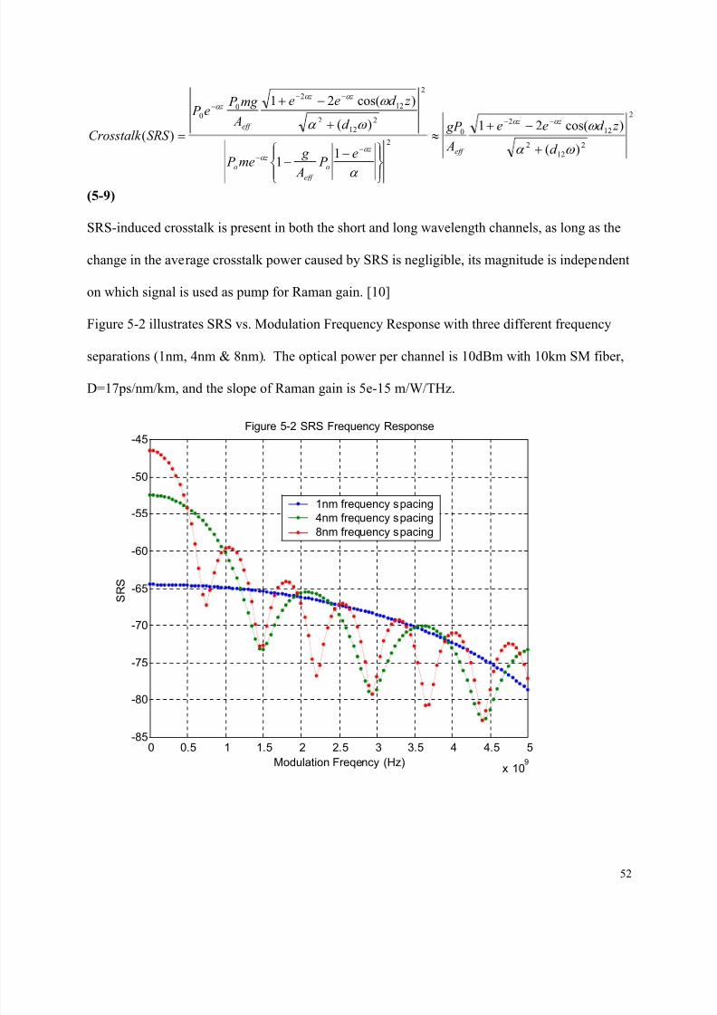
8/8/2019 Anthony Leung Thesis
http://slidepdf.com/reader/full/anthony-leung-thesis 61/116
52
2
2
12
2
12
2
0
2
2
2
12
2
12
2
00
)(
)cos(21
11
)(
)cos(21
)(ω α
ω
α
ω α
ω
α α
α α
α α
α
d
z d ee
A
gP
e P
A
g me P
d
z d ee
A
mg P e P
SRS Crosstalk
z z
eff z
o
eff
z
o
z z
eff
z
+
−+≈
−
−
+
−+
=−−
−−
−−−
(5-9)
SRS-induced crosstalk is present in both the short and long wavelength channels, as long as the
change in the average crosstalk power caused by SRS is negligible, its magnitude is independent
on which signal is used as pump for Raman gain. [10]
Figure 5-2 illustrates SRS vs. Modulation Frequency Response with three different frequency
separations (1nm, 4nm & 8nm). The optical power per channel is 10dBm with 10km SM fiber,
D=17ps/nm/km, and the slope of Raman gain is 5e-15 m/W/THz.
0 0.5 1 1.5 2 2.5 3 3.5 4 4.5 5
x 109
-85
-80
-75
-70
-65
-60
-55
-50
-45Figure 5-2 SRS Frequency Response
Modulation Freqency (Hz)
S R S
1nm frequency spacing
4nm frequency spacing
8nm frequency spacing

8/8/2019 Anthony Leung Thesis
http://slidepdf.com/reader/full/anthony-leung-thesis 62/116
53
We can summarize the characteristic of SRS Crosstalk Frequency Response as followed:
• As Frequency Separation (Wavelength Separation) increases, SRS crosstalk increases.
• SRS crosstalk decreases as modulation frequency increases when frequency separation >
1nm & SRS crosstalk stays constant as modulation frequency increases when frequency
separation is small, such as when less than 0.5nm.
• SRS crosstalk is dominant at large frequency separation with small modulation
frequency.
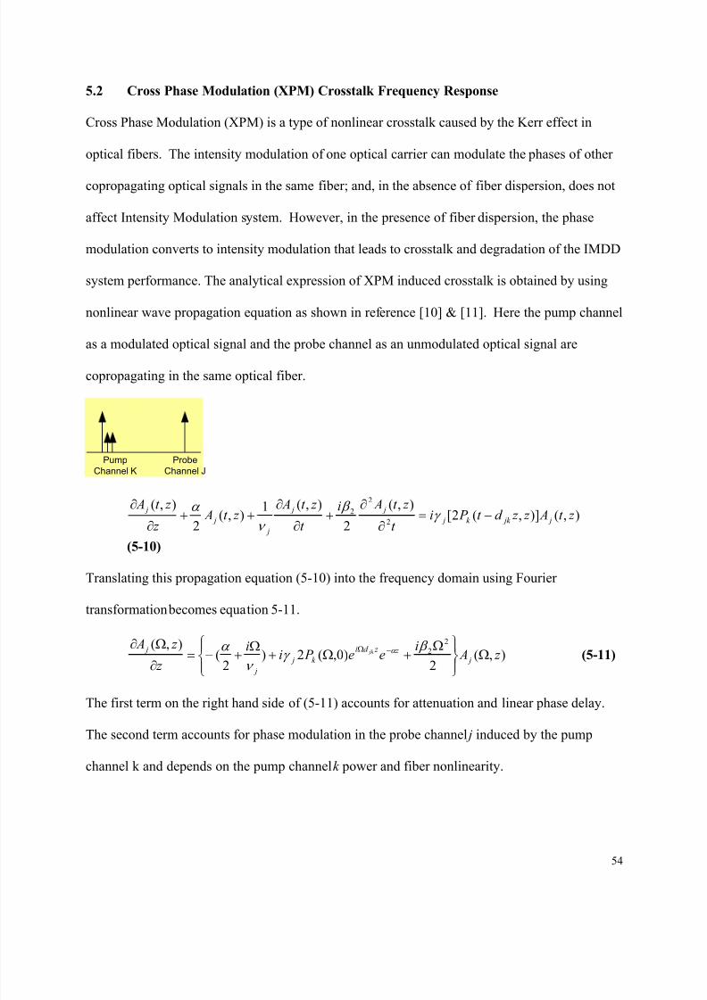
8/8/2019 Anthony Leung Thesis
http://slidepdf.com/reader/full/anthony-leung-thesis 63/116
54
5.2 Cross Phase Modulation (XPM) Crosstalk Frequency Response
Cross Phase Modulation (XPM) is a type of nonlinear crosstalk caused by the Kerr effect in
optical fibers. The intensity modulation of one optical carrier can modulate the phases of other
copropagating optical signals in the same fiber; and, in the absence of fiber dispersion, does not
affect Intensity Modulation system. However, in the presence of fiber dispersion, the phase
modulation converts to intensity modulation that leads to crosstalk and degradation of the IMDD
system performance. The analytical expression of XPM induced crosstalk is obtained by using
nonlinear wave propagation equation as shown in reference [10] & [11]. Here the pump channel
as a modulated optical signal and the probe channel as an unmodulated optical signal are
copropagating in the same optical fiber.
Pump
Channel K
Probe
Channel J
),()],(2[),(
2
),(1),(
2
),(
2
2
2 z t A z z d t P i
t
z t Ai
t
z t A z t A
z
z t A j jk k j
j j
j
j
j−=
∂
∂+
∂
∂++
∂
∂γ
β
ν
α
(5-10)
Translating this propagation equation (5-10) into the frequency domain using Fourier
transformation becomes equation 5-11.
),(2
)0,(2)2
(),( 2
2 z Ai
ee P ii
z
z A j
z z d i
k j
j
j jk Ω
Ω
+Ω+Ω
+−=∂
Ω∂−Ω β
γ ν
α α (5-11)
The first term on the right hand side of (5-11) accounts for attenuation and linear phase delay.
The second term accounts for phase modulation in the probe channel j induced by the pump
channel k and depends on the pump channel k power and fiber nonlinearity.
8/8/2019 Anthony Leung Thesis
http://slidepdf.com/reader/full/anthony-leung-thesis 64/116
55
In a short fiber section, dz, the crosstalk phase modulation in the probe signal induced by the
pump signal can be linearized under the small signal approximation [10],[11] In addition,
because of chromatic dispersion of the fiber, the crosstalk phase modulation generated at z=z’ is
converted into an amplitude modulation at the end of fiber z=L. Integrating all XPM
contributions along the fiber such as fiber loss, linear phase delay, phase modulation, phase
modulation to intensity modulation conversion, the total intensity noise at the end of fiber z=L
can be obtained as shown in reference [10], [11]
Ω−Ω−
−−
Ω+Ω−
−Ω=Ω∆
−ΩΩ−=Ω∆
Ω+−Ω
Ω+−Ω
Ω−
Ω−−Ω−−
∫
)2/()2/()0,(2)(),(
]2/)(sin[)0,(2)0(2),(
2
2
)(2
2
2
)(2
0
2
2
)()/(
2
2
2
2
β α β α γ
β γ
α β
α β
ν
α ν α
id ii
ee
id ii
ee P e L P L A
dz z Le P e P L A
jk
Ld i Li
jk
Ld i Li
k j
Li
j j
L z d i
k j
z i
j j
jk jk
j
jk j
and the XPM induced electrical power spectral density in the probe channel j is
2
2
2
)(2
2
2
)(2
2
)2/()2/()0,(2),(
)(
),(),(
22
22
Ω−Ω−−−
Ω+Ω−−Ω=Ω∆
Ω∆=Ω∆
Ω+−Ω
Ω+−Ω
β α β α γ
α
β
α
β
id ii
ee
id ii
ee P L P
L P
L A L P
jk
Ld i
Li
jk
Ld i
Li
k j j
j
j
j
jk jk
(5-12)
Figure 5-3 illustrates XPM vs. Modulation Frequency Response with three different
frequency separations (1nm, 4nm & 8nm). The average optical channel power is 10dBm with
10km SM fiber, D=17ps/nm/km.
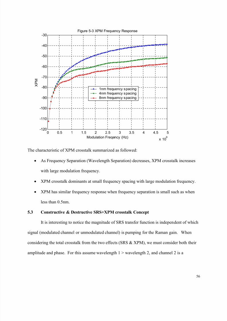
8/8/2019 Anthony Leung Thesis
http://slidepdf.com/reader/full/anthony-leung-thesis 65/116
56
0 0.5 1 1.5 2 2.5 3 3.5 4 4.5 5
x 109
-120
-110
-100
-90
-80
-70
-60
-50
-40
-30Figure 5-3 XPM Frequency Response
Modulation Freqency (Hz)
X P M
1nm frequency spacing
4nm frequency spacing
8nm frequency spacing
The characteristic of XPM crosstalk summarized as followed:
• As Frequency Separation (Wavelength Separation) decreases, XPM crosstalk increases
with large modulation frequency.
• XPM crosstalk dominants at small frequency spacing with large modulation frequency.
• XPM has similar frequency response when frequency separation is small such as when
less than 0.5nm.
5.3 Constructive & Destructive SRS+XPM crosstalk Concept
It is interesting to notice the magnitude of SRS transfer function is independent of which
signal (modulated channel or unmodulated channel) is pumping for the Raman gain. When
considering the total crosstalk from the two effects (SRS & XPM), we must consider both their
amplitude and phase. For this assume wavelength 1 > wavelength 2, and channel 2 is a
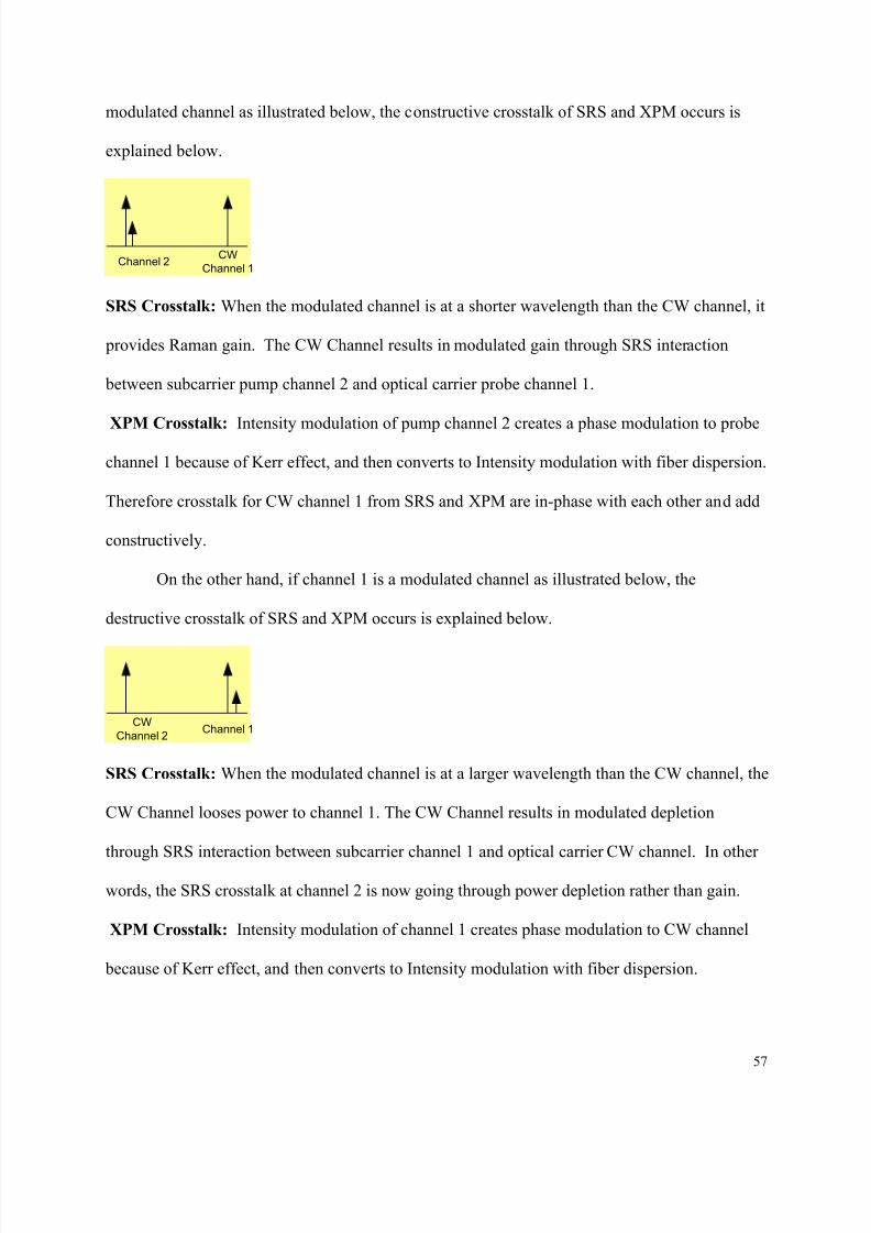
8/8/2019 Anthony Leung Thesis
http://slidepdf.com/reader/full/anthony-leung-thesis 66/116
57
modulated channel as illustrated below, the constructive crosstalk of SRS and XPM occurs is
explained below.
Channel 2CW
Channel 1
SRS Crosstalk: When the modulated channel is at a shorter wavelength than the CW channel, it
provides Raman gain. The CW Channel results in modulated gain through SRS interaction
between subcarrier pump channel 2 and optical carrier probe channel 1.
XPM Crosstalk: Intensity modulation of pump channel 2 creates a phase modulation to probe
channel 1 because of Kerr effect, and then converts to Intensity modulation with fiber dispersion.
Therefore crosstalk for CW channel 1 from SRS and XPM are in-phase with each other and add
constructively.
On the other hand, if channel 1 is a modulated channel as illustrated below, the
destructive crosstalk of SRS and XPM occurs is explained below.
CW
Channel 2Channel 1
SRS Crosstalk: When the modulated channel is at a larger wavelength than the CW channel, the
CW Channel looses power to channel 1. The CW Channel results in modulated depletion
through SRS interaction between subcarrier channel 1 and optical carrier CW channel. In other
words, the SRS crosstalk at channel 2 is now going through power depletion rather than gain.
XPM Crosstalk: Intensity modulation of channel 1 creates phase modulation to CW channel
because of Kerr effect, and then converts to Intensity modulation with fiber dispersion.
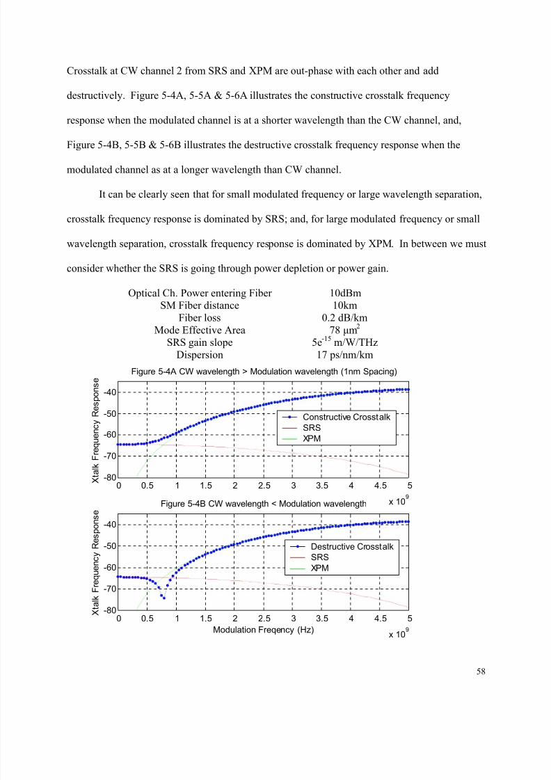
8/8/2019 Anthony Leung Thesis
http://slidepdf.com/reader/full/anthony-leung-thesis 67/116
58
Crosstalk at CW channel 2 from SRS and XPM are out-phase with each other and add
destructively. Figure 5-4A, 5-5A & 5-6A illustrates the constructive crosstalk frequency
response when the modulated channel is at a shorter wavelength than the CW channel, and,
Figure 5-4B, 5-5B & 5-6B illustrates the destructive crosstalk frequency response when the
modulated channel as at a longer wavelength than CW channel.
It can be clearly seen that for small modulated frequency or large wavelength separation,
crosstalk frequency response is dominated by SRS; and, for large modulated frequency or small
wavelength separation, crosstalk frequency response is dominated by XPM. In between we must
consider whether the SRS is going through power depletion or power gain.
Optical Ch. Power entering Fiber 10dBmSM Fiber distance 10km
Fiber loss 0.2 dB/km
Mode Effective Area 78 µm2
SRS gain slope 5e-15
m/W/THz
Dispersion 17 ps/nm/km
0 0.5 1 1.5 2 2.5 3 3.5 4 4.5 5
x 109
-80
-70
-60
-50
-40
Figure 5-4A CW wavelength > Modulation wavelength (1nm Spacing)
X t a l k F r e q u e n c y R e
s p o n s e
Constructive Crosstalk
SRS
XPM
0 0.5 1 1.5 2 2.5 3 3.5 4 4.5 5
x 109
-80
-70
-60
-50
-40
Figure 5-4B CW wavelength < Modulation wavelength
Modulation Freqency (Hz)
X t a l k F r e q u e n c y R
e s p o n s e
Destructive CrosstalkSRS
XPM
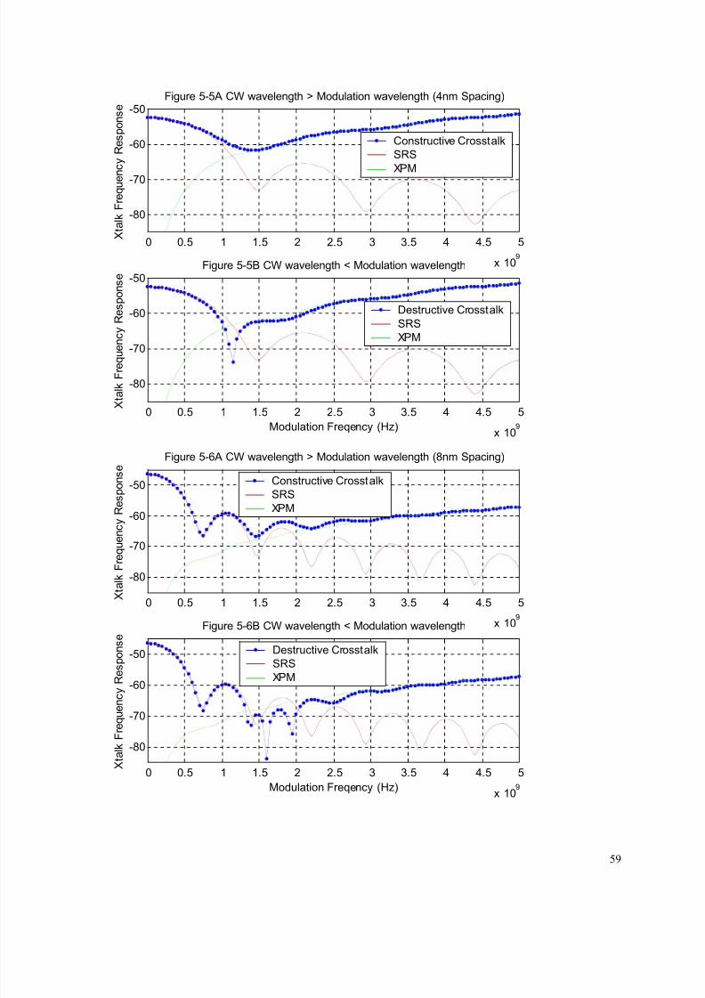
8/8/2019 Anthony Leung Thesis
http://slidepdf.com/reader/full/anthony-leung-thesis 68/116
59
0 0.5 1 1.5 2 2.5 3 3.5 4 4.5 5
x 109
-80
-70
-60
-50Figure 5-5A CW wavelength > Modulation wavelength (4nm Spacing)
X t a l k F r e q u e n
c y R e s p o n s e
Constructive Crosstalk
SRS
XPM
0 0.5 1 1.5 2 2.5 3 3.5 4 4.5 5
x 109
-80
-70
-60
-50Figure 5-5B CW wavelength < Modulation wavelength
Modulation Freqency (Hz)
X t a l k F r e q u e
n c y R e s p o n s e
Destructive Crosstalk
SRS
XPM
0 0.5 1 1.5 2 2.5 3 3.5 4 4.5 5
x 109
-80
-70
-60
-50
Figure 5-6A CW wavelength > Modulation wavelength (8nm Spacing)
X t a l k F r e q u e n c y R e s p o n s e
Constructive Crosstalk
SRS
XPM
0 0.5 1 1.5 2 2.5 3 3.5 4 4.5 5
x 109
-80
-70
-60
-50
Figure 5-6B CW wavelength < Modulation wavelength
Modulation Freqency (Hz)
X t a l k F r e q u e n c y R e s p o n s e
Destructive Crosstalk
SRS
XPM
8/8/2019 Anthony Leung Thesis
http://slidepdf.com/reader/full/anthony-leung-thesis 69/116
60
5.4 SRS and XPM Crosstalk in SCM externally modulated optical link
In this section, we examine SRS & XPM crosstalk interaction between subcarrier
channels (analog and digital) within the same wavelength. Equation (5-4) can be re-modified by
assuming the two (2) subcarrier channels are ))cos((),0( 202 t m P t P ω = and
))cos((),0( 101 t m P t P ω = , which have the same average optical power and OMI.
Assuming subcarrier 2 RF frequency > subcarrier 1 RF frequency: the SRS crosstalk at
subcarrier 2 suffers by subcarrier channel 1
++⋅= ∫
−− z z
eff
z
o dz e z d m P
A
g em P P
0
''
121110222
'
)cos(1)cos(),0(α α
ω µ ω ωµ µ (5-13)
where the first term corresponds to pump subcarrier after fiber loss and the second term is the
crosstalk terms which correspond to the SRS interaction between pump and probe subcarriers.
This SRS crosstalk is a result of power gain. The SRS crosstalk level in electrical domain can be
expressed as following:
2
2
12
2
12
2
0
2
0
2
2
12
2
12
2
00
)(
)cos(21)()cos(21
)(ω α
ω ω α ω
α α
α
α α
α
d
z d ee
A
m gP
me P
d z d ee
Amg P me P
SRS Crosstalk
z z
eff z
z z
eff
z
+
−+=
+
−+
=−−
−
−−
−
(5-14)
where P 0m is the optical power of RF channel.
Before we analyze SRS & XPM crosstalk between analog and digital SCM/WDM
system, it is important to address the sensitivity of the probe channel to SRS & XPM induced
crosstalk is related on its receiver bandwidth, therefore, the crosstalk between high and low bit
rate channels is comparable to the crosstalk between two low bit rate channels [10]. In this
project, we have assumed that the crosstalk level between 1Gb/s digital data & 6MHz analog
channel is comparable to the crosstalk between two 6MHz analog channels.
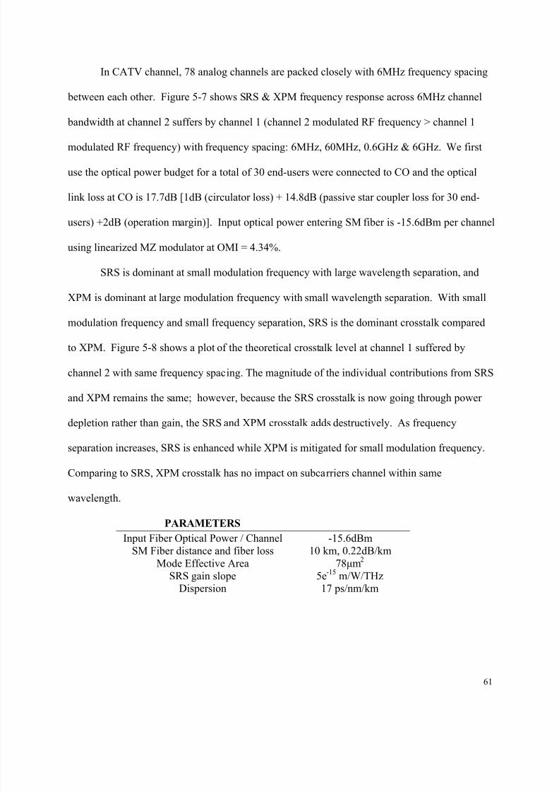
8/8/2019 Anthony Leung Thesis
http://slidepdf.com/reader/full/anthony-leung-thesis 70/116
61
In CATV channel, 78 analog channels are packed closely with 6MHz frequency spacing
between each other. Figure 5-7 shows SRS & XPM frequency response across 6MHz channel
bandwidth at channel 2 suffers by channel 1 (channel 2 modulated RF frequency > channel 1
modulated RF frequency) with frequency spacing: 6MHz, 60MHz, 0.6GHz & 6GHz. We first
use the optical power budget for a total of 30 end-users were connected to CO and the optical
link loss at CO is 17.7dB [1dB (circulator loss) + 14.8dB (passive star coupler loss for 30 end-
users) +2dB (operation margin)]. Input optical power entering SM fiber is -15.6dBm per channel
using linearized MZ modulator at OMI = 4.34%.
SRS is dominant at small modulation frequency with large wavelength separation, and
XPM is dominant at large modulation frequency with small wavelength separation. With small
modulation frequency and small frequency separation, SRS is the dominant crosstalk compared
to XPM. Figure 5-8 shows a plot of the theoretical crosstalk level at channel 1 suffered by
channel 2 with same frequency spacing. The magnitude of the individual contributions from SRS
and XPM remains the same; however, because the SRS crosstalk is now going through power
depletion rather than gain, the SRS and XPM crosstalk adds destructively. As frequency
separation increases, SRS is enhanced while XPM is mitigated for small modulation frequency.
Comparing to SRS, XPM crosstalk has no impact on subcarriers channel within same
wavelength.
PARAMETERS
Input Fiber Optical Power / Channel -15.6dBm
SM Fiber distance and fiber loss 10 km, 0.22dB/kmMode Effective Area 78µm2
SRS gain slope 5e-15
m/W/THzDispersion 17 ps/nm/km
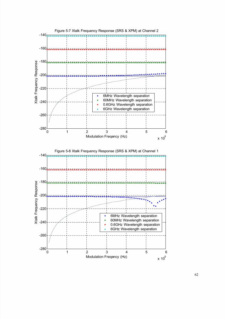
8/8/2019 Anthony Leung Thesis
http://slidepdf.com/reader/full/anthony-leung-thesis 71/116
62
0 1 2 3 4 5 6
x 106
-280
-260
-240
-220
-200
-180
-160
-140Figure 5-7 Xtalk Frequency Response (SRS & XPM) at Channel 2
Modulation Freqency (Hz)
X t a l k F r e q u e n c y R e s p o n s e
6MHz Wavelength separation
60MHz Wavelength separation
0.6GHz Wavelength separation
6GHz Wavelength separation
0 1 2 3 4 5 6
x 106
-280
-260
-240
-220
-200
-180
-160
-140Figure 5-8 Xtalk Frequency Response (SRS & XPM) at Channel 1
Modulation Freqency (Hz)
X
t a l k F r e q u e n c y R e s p o n s e
6MHz Wavelength separation
60MHz Wavelength separation
0.6GHz Wavelength separation6GHz Wavelength separation
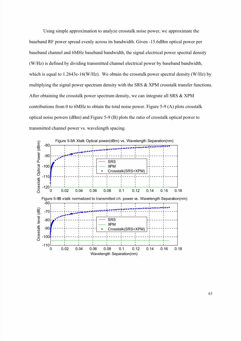
8/8/2019 Anthony Leung Thesis
http://slidepdf.com/reader/full/anthony-leung-thesis 72/116
63
Using simple approximation to analyze crosstalk noise power, we approximate the
baseband RF power spread evenly across its bandwidth. Given -15.6dBm optical power per
baseband channel and 6MHz baseband bandwidth, the signal electrical power spectral density
(W/Hz) is defined by dividing transmitted channel electrical power by baseband bandwidth,
which is equal to 1.2643e-16(W/Hz). We obtain the crosstalk power spectral density (W/Hz) by
multiplying the signal power spectrum density with the SRS & XPM crosstalk transfer functions.
After obtaining the crosstalk power spectrum density, we can integrate all SRS & XPM
contributions from 0 to 6MHz to obtain the total noise power. Figure 5-9 (A) plots crosstalk
optical noise powers (dBm) and Figure 5-9 (B) plots the ratio of crosstalk optical power to
transmitted channel power vs. wavelength spacing.
0 0.02 0.04 0.06 0.08 0.1 0.12 0.14 0.16 0.18-120
-110
-100
-90
-80Figure 5-9A Xtalk Optical power(dBm) vs. Wavelength Separation(nm)
C r o s s t a l k O p t i c a l P o w e r ( d B m )
SRS
XPM
Crosstalk(SRS+XPM)
0 0.02 0.04 0.06 0.08 0.1 0.12 0.14 0.16 0.18-110
-100
-90
-80
-70
-60Figure 5-9B xtalk normalized to transmitted ch. power vs. Wavelength Separation(nm)
Wavelength Separation(nm)
C r o s s t a l k l e v e l ( d B )
SRS
XPM
Crosstalk(SRS+XPM)

8/8/2019 Anthony Leung Thesis
http://slidepdf.com/reader/full/anthony-leung-thesis 73/116
64
The SRS & XPM induced crosstalk between subcarriers in the same wavelength is
summarized as follows:
• Compared to XPM, SRS is the dominant crosstalk in small signal bandwidth and small
frequency spacing.
• Because of small channel bandwidth and small optical channel power, SRS-induced
crosstalk is independent of which subcarrier channel is the pump for the Raman gain.
• Overall result, SRS & XPM Crosstalk show very minimal impact between two subcarrier
channels in the same wavelength.
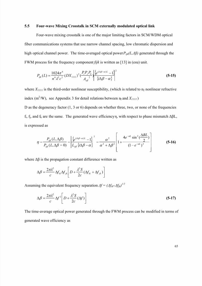
8/8/2019 Anthony Leung Thesis
http://slidepdf.com/reader/full/anthony-leung-thesis 74/116
65
5.5 Four-wave Mixing Crosstalk in SCM externally modulated optical link
Four-wave mixing crosstalk is one of the major limiting factors in SCM/WDM optical
fiber communications systems that use narrow channel spacing, low chromatic dispersion and
high optical channel power. The time-averaged optical power P ijk (L, β ) generated through the
FWM process for the frequency component fijk is written as [13] in (esu) unit.
2)(
2
2
1111224
6 1)()(
1024)(
α β λ
π α β
−∆
−=
−∆
i
e
A
P P P DX
cn L P
Li
eff
k ji
ijk (5-15)
where X 1111 is the third-order nonlinear susceptibility, (which is related to n2 nonlinear refractive
index (m
2
/W), see Appendix 3 for detail relations between n2 and Χ 1111 )
D as the degeneracy factor (1, 3 or 6) depends on whether three, two, or none of the frequencies
f i, f j, and f k are the same. The generated wave efficiency η, with respect to phase mismatch ∆βL,
is expressed as
−
∆
+∆+
=−∆
−=
=∆
∆=
−
−−∆
2
2
22
22
)(
)1(
)2
(sin4
11
)0,(
),( L
L
eff
Li
ijk
ijk
e
BLe
i L
e
L P
L P α
α α β
β α
α
α β β
β η (5-16)
where ∆β is the propagation constant difference written as
∆+∆+∆∆=∆ )(
2
2 22
jk ik jk ik f f c
S D f f
c
λ πλ β
Assuming the equivalent frequency separation f = ( f ik* f jk )1/2
∆+∆=∆ )(
2
2 22
2
f c
S D f
c
λ πλ β (5-17)
The time-average optical power generated through the FWM process can be modified in terms of
generated wave efficiency as
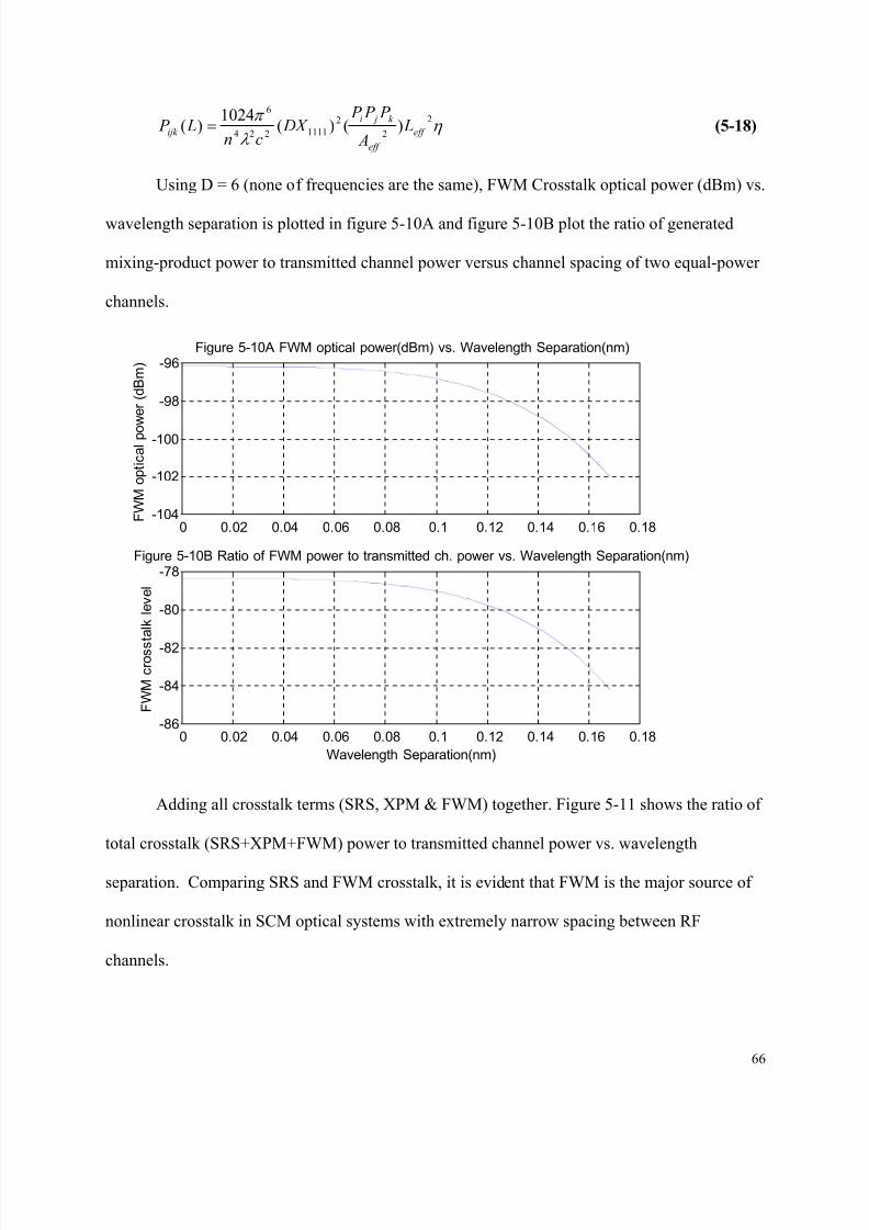
8/8/2019 Anthony Leung Thesis
http://slidepdf.com/reader/full/anthony-leung-thesis 75/116
66
η λ
π 2
2
2
1111224
6
)()(1024
)( eff
eff
k ji
ijk L A
P P P DX
cn L P = (5-18)
Using D = 6 (none of frequencies are the same), FWM Crosstalk optical power (dBm) vs.
wavelength separation is plotted in figure 5-10A and figure 5-10B plot the ratio of generated
mixing-product power to transmitted channel power versus channel spacing of two equal-power
channels.
0 0.02 0.04 0.06 0.08 0.1 0.12 0.14 0.16 0.18-104
-102
-100
-98
-96Figure 5-10A FWM optical power(dBm) vs. Wavelength Separation(nm)
F W M o p t i c a l p o
w e r ( d B m )
0 0.02 0.04 0.06 0.08 0.1 0.12 0.14 0.16 0.18-86
-84
-82
-80
-78Figure 5-10B Ratio of FWM power to transmitted ch. power vs. Wavelength Separation(nm)
Wavelength Separation(nm)
F W M c r o s s
t a l k l e v e l
Adding all crosstalk terms (SRS, XPM & FWM) together. Figure 5-11 shows the ratio of
total crosstalk (SRS+XPM+FWM) power to transmitted channel power vs. wavelength
separation. Comparing SRS and FWM crosstalk, it is evident that FWM is the major source of
nonlinear crosstalk in SCM optical systems with extremely narrow spacing between RF
channels.
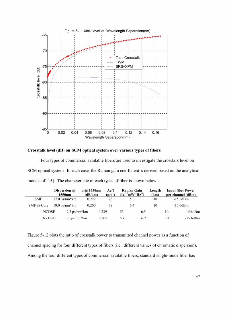
8/8/2019 Anthony Leung Thesis
http://slidepdf.com/reader/full/anthony-leung-thesis 76/116
67
0 0.02 0.04 0.06 0.08 0.1 0.12 0.14 0.16-95
-90
-85
-80
-75
-70
-65Figure 5-11 Xtalk level vs. Wavelength Separation(nm)
Wavelength Separation(nm)
C r o s s t a l k l e v e l ( d B )
Total Crosstalk
FWM
SRS+XPM
Crosstalk level (dB) on SCM optical system over various types of fibers
Four types of commercial available fibers are used to investigate the crosstalk level on
SCM optical system. In each case, the Raman gain coefficient is derived based on the analytical
models of [15]. The characteristic of each types of fiber is shown below.
Dispersion @
1550nm
α @ 1550nm
(dB/km)
Aeff
(µm2)
Raman Gain
(1e-27
mW-1
Hz-1
) Length
(km)
Input fiber Power
per channel (dBm)
SMF 17.0 ps/nm*km 0.222 78 5.0 10 -15.6dBm
SMF Si-Core 19.0 ps/nm*km 0.200 78 6.4 10 -15.6dBm
NZDSF- -2.3 ps/nm*km 0.239 53 6.5 10 -15.6dBm
NZDSF+ 3.0 ps/nm*km 0.205 53 6.7 10 -15.6dBm
Figure 5-12 plots the ratio of crosstalk power to transmitted channel power as a function of
channel spacing for four different types of fibers (i.e., different values of chromatic dispersion).
Among the four different types of commercial available fibers, standard single-mode fiber has
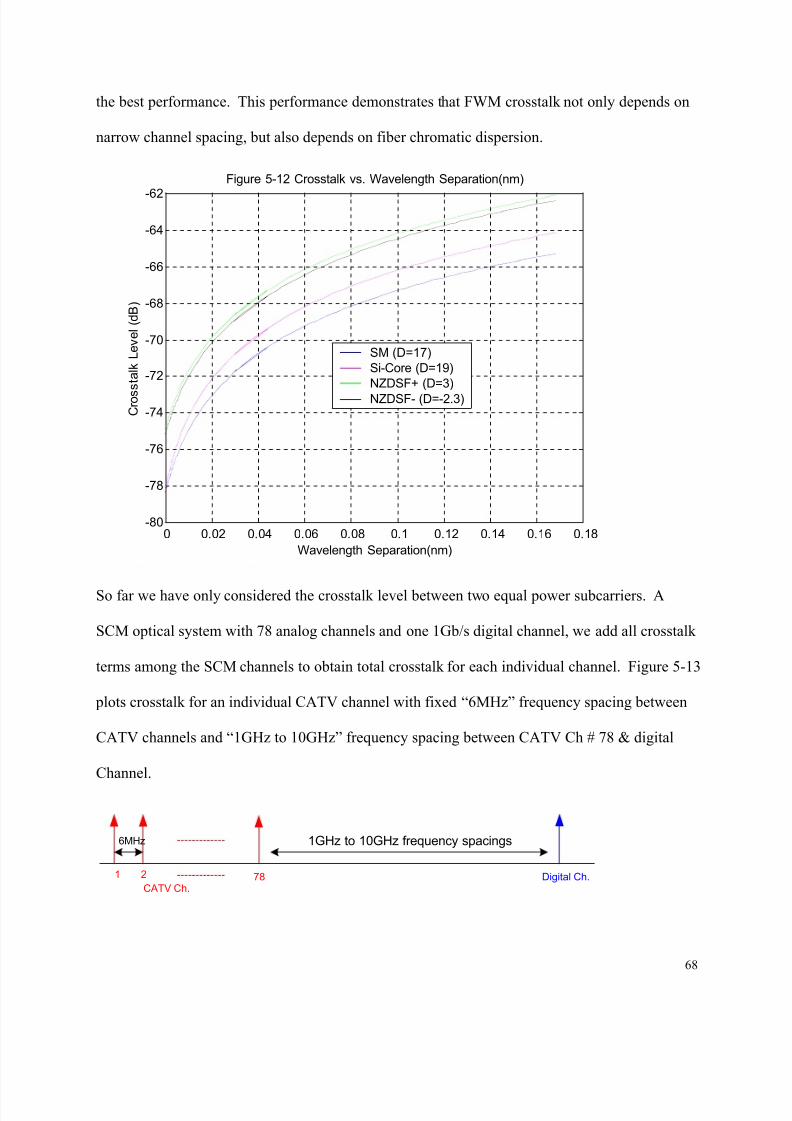
8/8/2019 Anthony Leung Thesis
http://slidepdf.com/reader/full/anthony-leung-thesis 77/116
68
the best performance. This performance demonstrates that FWM crosstalk not only depends on
narrow channel spacing, but also depends on fiber chromatic dispersion.
0 0.02 0.04 0.06 0.08 0.1 0.12 0.14 0.16 0.18-80
-78
-76
-74
-72
-70
-68
-66
-64
-62
Figure 5-12 Crosstalk vs. Wavelength Separation(nm)
Wavelength Separation(nm)
C r o s s t a l k L e v e l ( d B )
SM (D=17)
Si-Core (D=19)
NZDSF+ (D=3)
NZDSF- (D=-2.3)
So far we have only considered the crosstalk level between two equal power subcarriers. A
SCM optical system with 78 analog channels and one 1Gb/s digital channel, we add all crosstalk
terms among the SCM channels to obtain total crosstalk for each individual channel. Figure 5-13
plots crosstalk for an individual CATV channel with fixed “6MHz” frequency spacing between
CATV channels and “1GHz to 10GHz” frequency spacing between CATV Ch # 78 & digital
Channel.
CATV Ch.Digital Ch.1 2 78
1GHz to 10GHz frequency spacings6MHz
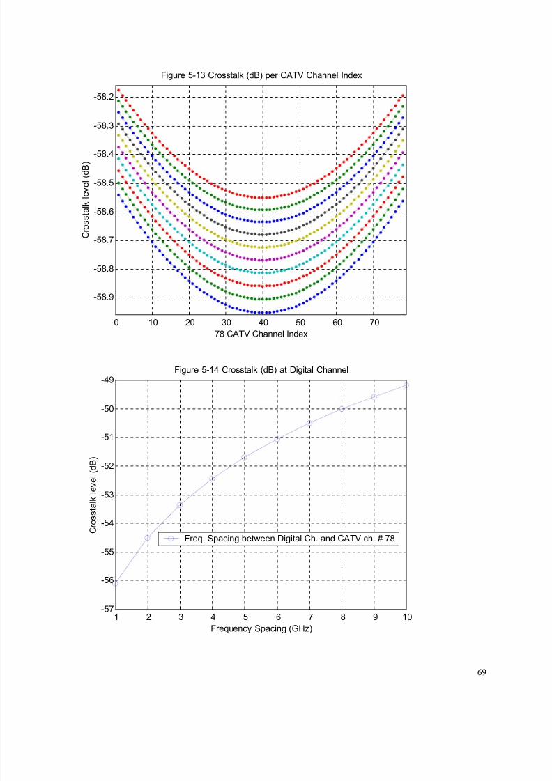
8/8/2019 Anthony Leung Thesis
http://slidepdf.com/reader/full/anthony-leung-thesis 78/116
69
0 10 20 30 40 50 60 70
-58.9
-58.8
-58.7
-58.6
-58.5
-58.4
-58.3
-58.2
Figure 5-13 Crosstalk (dB) per CATV Channel Index
C r o s s t a l k l e v e l ( d B )
78 CATV Channel Index
1 2 3 4 5 6 7 8 9 10-57
-56
-55
-54
-53
-52
-51
-50
-49Figure 5-14 Crosstalk (dB) at Digital Channel
Frequency Spacing (GHz)
C r o s s t a l k l e v e l ( d B )
Freq. Spacing between Digital Ch. and CATV ch. # 78
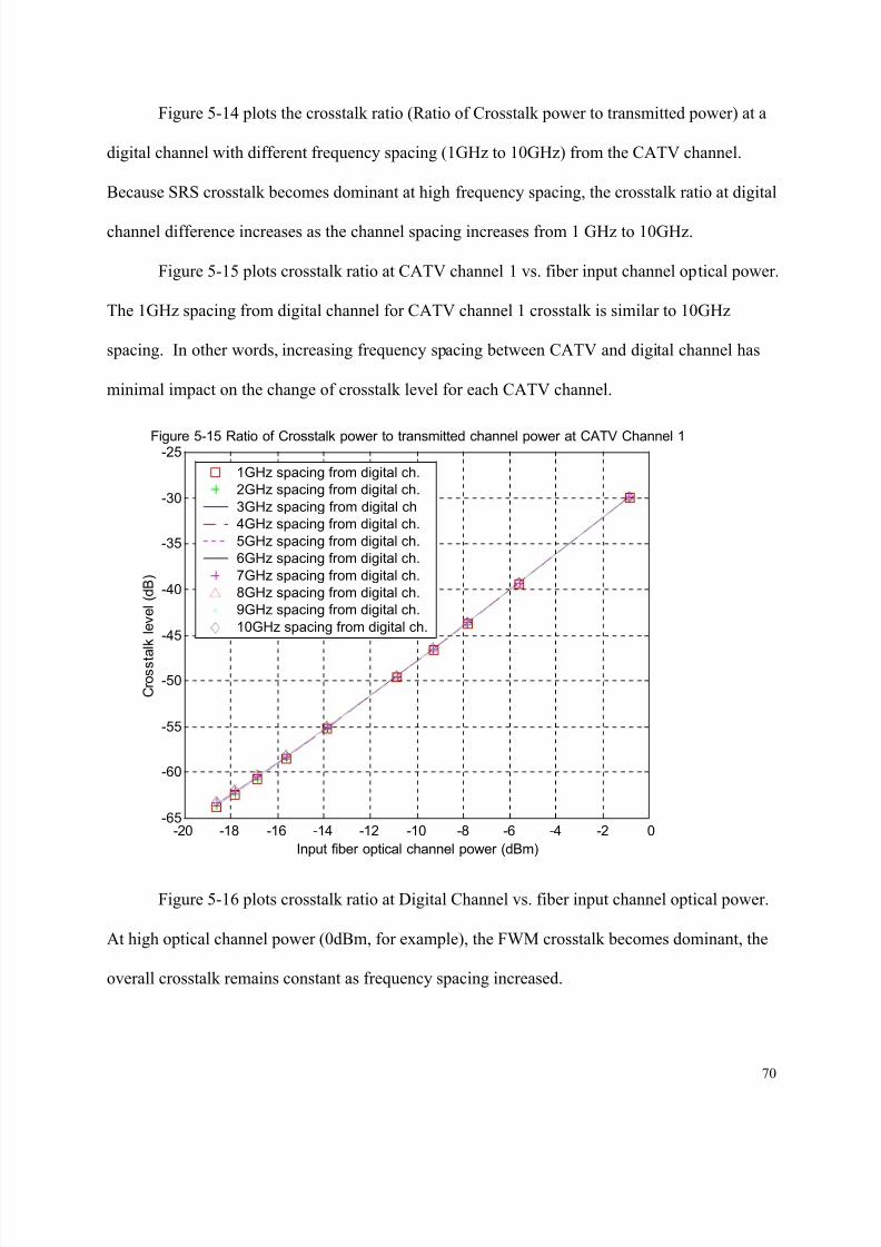
8/8/2019 Anthony Leung Thesis
http://slidepdf.com/reader/full/anthony-leung-thesis 79/116
70
Figure 5-14 plots the crosstalk ratio (Ratio of Crosstalk power to transmitted power) at a
digital channel with different frequency spacing (1GHz to 10GHz) from the CATV channel.
Because SRS crosstalk becomes dominant at high frequency spacing, the crosstalk ratio at digital
channel difference increases as the channel spacing increases from 1 GHz to 10GHz.
Figure 5-15 plots crosstalk ratio at CATV channel 1 vs. fiber input channel optical power.
The 1GHz spacing from digital channel for CATV channel 1 crosstalk is similar to 10GHz
spacing. In other words, increasing frequency spacing between CATV and digital channel has
minimal impact on the change of crosstalk level for each CATV channel.
-20 -18 -16 -14 -12 -10 -8 -6 -4 -2 0-65
-60
-55
-50
-45
-40
-35
-30
-25Figure 5-15 Ratio of Crosstalk power to transmitted channel power at CATV Channel 1
Input fiber optical channel power (dBm)
C r o s s t a
l k l e v e l ( d B )
1GHz spacing from digital ch.
2GHz spacing from digital ch.
3GHz spacing from digital ch
4GHz spacing from digital ch.
5GHz spacing from digital ch.
6GHz spacing from digital ch.
7GHz spacing from digital ch.
8GHz spacing from digital ch.
9GHz spacing from digital ch.
10GHz spacing from digital ch.
Figure 5-16 plots crosstalk ratio at Digital Channel vs. fiber input channel optical power.
At high optical channel power (0dBm, for example), the FWM crosstalk becomes dominant, the
overall crosstalk remains constant as frequency spacing increased.
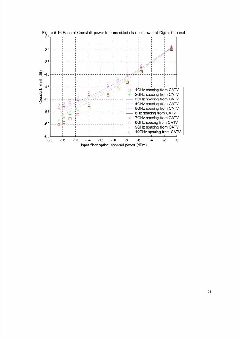
8/8/2019 Anthony Leung Thesis
http://slidepdf.com/reader/full/anthony-leung-thesis 80/116
71
-20 -18 -16 -14 -12 -10 -8 -6 -4 -2 0-65
-60
-55
-50
-45
-40
-35
-30
-25Figure 5-16 Ratio of Crosstalk power to transmitted channel power at Digital Channel
Input fiber optical channel power (dBm)
C r o s s t a l k l e v e l ( d B )
1GHz spacing from CATV
2GHz spacing from CATV
3GHz spacing from CATV
4GHz spacing from CATV
5GHz spacing from CATV
6Hz spacing from CATV
7GHz spacing from CATV8GHz spacng from CATV
9GHz spacing from CATV
10GHz spacing from CATV
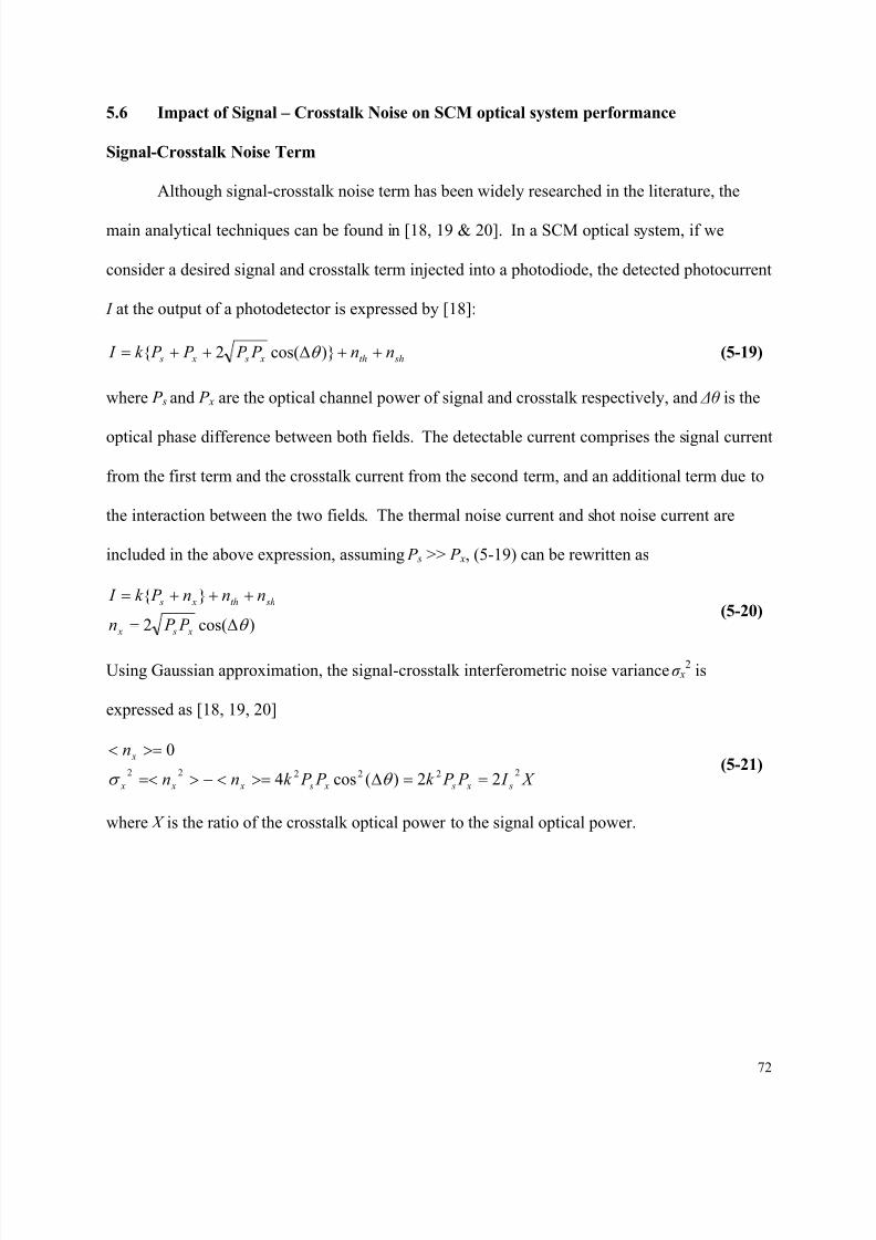
8/8/2019 Anthony Leung Thesis
http://slidepdf.com/reader/full/anthony-leung-thesis 81/116
72
5.6 Impact of Signal – Crosstalk Noise on SCM optical system performance
Signal-Crosstalk Noise Term
Although signal-crosstalk noise term has been widely researched in the literature, the
main analytical techniques can be found in [18, 19 & 20]. In a SCM optical system, if we
consider a desired signal and crosstalk term injected into a photodiode, the detected photocurrent
I at the output of a photodetector is expressed by [18]:
shth x s x s nn P P P P k I ++∆++= )cos(2 θ (5-19)
where P s and P x are the optical channel power of signal and crosstalk respectively, and θ is the
optical phase difference between both fields. The detectable current comprises the signal current
from the first term and the crosstalk current from the second term, and an additional term due to
the interaction between the two fields. The thermal noise current and shot noise current are
included in the above expression, assuming P s >> P x, (5-19) can be rewritten as
)cos(2
θ ∆=
+++=
x s x
shth x s
P P n
nnn P k I (5-20)
Using Gaussian approximation, the signal-crosstalk interferometric noise variance σ x2
is
expressed as [18, 19, 20]
X I P P k P P k nn
n
s x s x s x x x
x
22222222)(cos4
0
==∆>=<−>=<
>=<
θ σ (5-21)
where X is the ratio of the crosstalk optical power to the signal optical power.
8/8/2019 Anthony Leung Thesis
http://slidepdf.com/reader/full/anthony-leung-thesis 82/116
73
5.7 CATV CNR include signal-crosstalk noise term
SCM Optical transmission performance including RIN noise, Thermal noise, Shot noise,
ASE noise, Clipping noise, Nonlinear Distortion as well as Signal-crosstalk noise term is
analyzed in this section. Use the best case linearized Dual parallel MZ Modulators with A=0.93
and B=2.5 and same parameter values as discussed in section 4.3., the comparison of Case I & II
CATV CNR with and without signal-crosstalk noise terms versus optical channel power is
plotted in figure 5-17.
PARAMETERS Case 1 Case 2
Linearized MZ Modulator A=0.93 & B=2.5 A=0.93 & B=2.5
Input power at Booster Amplifier -1dBm 3dBmLaser RIN -155dB/Hz -160dB/Hz
Photodiode Responsivity 0.8 A/W 0.9 A/W
Fiber distance 10km 10km
OMI 4.343% 4.343%
As optical channel power increases, crosstalk noise increases and degrades system performance.
The plot shows the highest CNR includes crosstalk noise term is 48.5dB using Case I model. It
indicates that as long as the receiver optical channel power is in the range of -20dBm to -17dBm,
we can obtain CNR up to 48dB or higher. Figure 5-18 plots CNR vs. number of customer
premises. It shows the SCM optical system required to connect at least 20 but no more than 40
customer units to meet 48dB CNR. With this understanding, it is important to optimize the
practical optical link budget to meet the system performance.
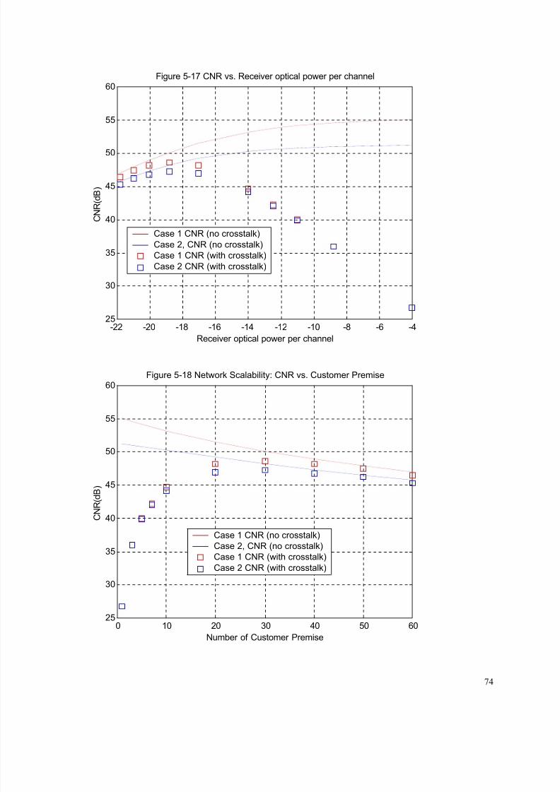
8/8/2019 Anthony Leung Thesis
http://slidepdf.com/reader/full/anthony-leung-thesis 83/116
74
-22 -20 -18 -16 -14 -12 -10 -8 -6 -425
30
35
40
45
50
55
60Figure 5-17 CNR vs. Receiver optical power per channel
Receiver optical power per channel
C N R ( d B )
Case 1 CNR (no crosstalk)
Case 2, CNR (no crosstalk)
Case 1 CNR (with crosstalk)
Case 2 CNR (with crosstalk)
0 10 20 30 40 50 6025
30
35
40
45
50
55
60Figure 5-18 Network Scalability: CNR vs. Customer Premise
Number of Customer Premise
C N R ( d B )
Case 1 CNR (no crosstalk)
Case 2, CNR (no crosstalk)
Case 1 CNR (with crosstalk)Case 2 CNR (with crosstalk)
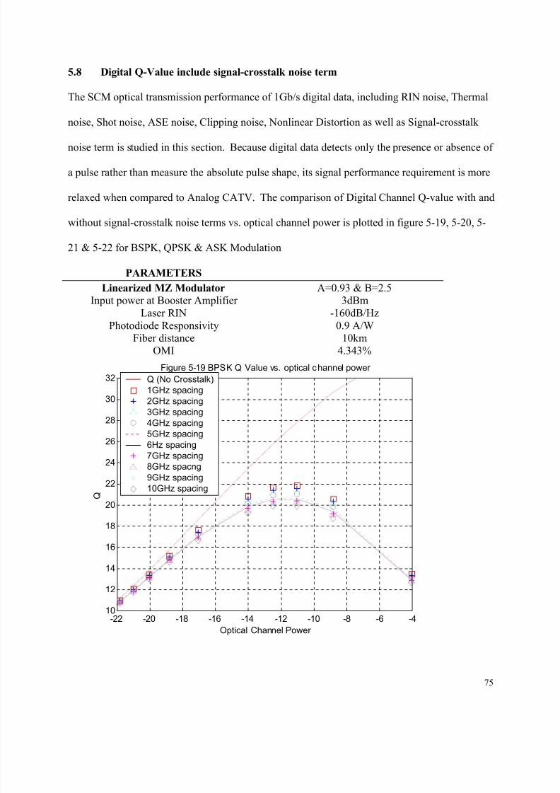
8/8/2019 Anthony Leung Thesis
http://slidepdf.com/reader/full/anthony-leung-thesis 84/116
75
5.8 Digital Q-Value include signal-crosstalk noise term
The SCM optical transmission performance of 1Gb/s digital data, including RIN noise, Thermal
noise, Shot noise, ASE noise, Clipping noise, Nonlinear Distortion as well as Signal-crosstalk
noise term is studied in this section. Because digital data detects only the presence or absence of
a pulse rather than measure the absolute pulse shape, its signal performance requirement is more
relaxed when compared to Analog CATV. The comparison of Digital Channel Q-value with and
without signal-crosstalk noise terms vs. optical channel power is plotted in figure 5-19, 5-20, 5-
21 & 5-22 for BSPK, QPSK & ASK Modulation
PARAMETERSLinearized MZ Modulator A=0.93 & B=2.5
Input power at Booster Amplifier 3dBm
Laser RIN -160dB/Hz
Photodiode Responsivity 0.9 A/WFiber distance 10km
OMI 4.343%
-22 -20 -18 -16 -14 -12 -10 -8 -6 -410
12
14
16
18
20
22
24
26
28
30
32Figure 5-19 BPSK Q Value vs. optical channel power
Optical Channel Power
Q
Q (No Crosstalk)
1GHz spacing
2GHz spacing
3GHz spacing
4GHz spacing
5GHz spacing
6Hz spacing
7GHz spacing
8GHz spacng
9GHz spacing
10GHz spacing
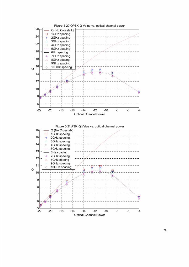
8/8/2019 Anthony Leung Thesis
http://slidepdf.com/reader/full/anthony-leung-thesis 85/116
76
-22 -20 -18 -16 -14 -12 -10 -8 -6 -4
6
8
10
12
14
16
18
20
22
24
26Figure 5-20 QPSK Q Value vs. optical channel power
Optical Channel Power
Q
Q (No Crosstalk)
1GHz spacing
2GHz spacing
3GHz spacing
4GHz spacing
5GHz spacing
6Hz spacing
7GHz spacing
8GHz spacng
9GHz spacing
10GHz spacing
-22 -20 -18 -16 -14 -12 -10 -8 -6 -45
6
7
8
9
10
11
12
13
14
15
16Figure 5-21 ASK Q Value vs. optical channel power
Optical Channel Power
Q
Q (No Crosstalk)
1GHz spacing
2GHz spacing
3GHz spacing4GHz spacing
5GHz spacing
6Hz spacing
7GHz spacing
8GHz spacng
9GHz spacing
10GHz spacing
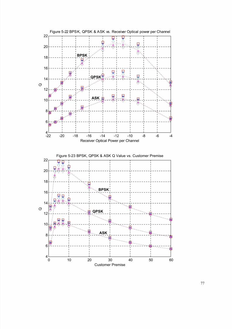
8/8/2019 Anthony Leung Thesis
http://slidepdf.com/reader/full/anthony-leung-thesis 86/116
77
-22 -20 -18 -16 -14 -12 -10 -8 -6 -44
6
8
10
12
14
16
18
20
22Figure 5-22 BPSK, QPSK & ASK vs. Receiver Optical power per Channel
Receiver Optical Power per Channel
Q
BPSK
QPSK
ASK
0 10 20 30 40 50 604
6
8
10
12
14
16
18
20
22Figure 5-23 BPSK, QPSK & ASK Q Value vs. Customer Premise
Customer Premise
Q
BPSK
QPSK
ASK
8/8/2019 Anthony Leung Thesis
http://slidepdf.com/reader/full/anthony-leung-thesis 87/116
78
Figure 5-23 plots Digital Q-value vs. number of customer premises. Based on the theoretical
analysis, the transmission performance to be expected from a SCM optical system supporting 78
CATV and 1Gb/s digital data from central office to customer premises is summarized as follows:
1) The desirable receiver optical power per channel is in the range of -20dBm to -17dBm in
order to achieve the maximum CNR.
2) The Optical Power (rms) contains 79 modulated RF signals at Receiver can be calculated
as -10.5dBm to -7.5dBm.
3) The RF channel power at the output of photodiode is calculated as -90dBm to -84.9dBm
using Responsivity =0.9 and Circuit Resistance = 50ohms.
4) CATV CNR = 48dB to 48.5dB.
5) Digital BPSK Q = 13 to 17.
6) Digital QPSK Q = 9 to 12.
7) Digital ASK Q = 6 to 8.
8) Number of Customer premises = 20 to 40.
8/8/2019 Anthony Leung Thesis
http://slidepdf.com/reader/full/anthony-leung-thesis 88/116
79
CHAPTER 6: Conclusion & Future Work
6.1 Conclusion
This project analyzed the transmission performance of SCM Optical system transmitting
78 CATV analog and 1Gb/s digital data from CO to customer premises. This study demonstrates
that using OSSB modulation, all even-order nonlinear distortion generated by MZ modulator can
be cancelled by biasing the modulator at Q point. Also, the third order distortion generated by
the MZ modulator can be suppressed using linearized dual parallel modulators. Three scenarios
were studied to optimize the CTB suppression. The best result occurs when the setting of the
optical power splitting ratio is 0.93 at the primary MZ modulator and the RF power ratio is 2.5 at
the secondary MZ modulator. The analytical results of this study demonstrate that the scalability
of this SCM externally modulated optical network, excluding the fiber nonlinear impact, can
connect as many as 30 customers. With such optical power budget, the quality of CATV can
achieve 50dB CNR or higher and the third order distortion of 60dBc or higher. In addition to
CATV, the performance of downstream digital data shows good analytical results.
• BPSK modulation results in Q value equal to 15
• QPSK modulation results in Q value equal to 11
• ASK modulation results the Q value equal to 7
The results are due to the high optical power transmission in the SCM externally modulated
network and because the digital signal performance requirement is a more relax compared to
analog CATV.
However, we’ve seen in addition to noise terms such as thermal, shot, ASE, RIN,
clipping, non-linear distortion generated from the system transmitter, the MZ modulator and
receivers, the fiber nonlinear crosstalk plays an important role in determining the overall network
8/8/2019 Anthony Leung Thesis
http://slidepdf.com/reader/full/anthony-leung-thesis 89/116
80
transmission performance. SRS, XPM and FWM are studied in this project. Because the
sensitivity of probe channel to induced crosstalk is related on its receiver bandwidth, the
crosstalk level between high and small bandwidth channels is comparable to the crosstalk
between two small bandwidth channels [10]. In other words, the crosstalk level between 1Gb/s
digital channel and CATV channel is comparable to the crosstalk between two CATV channels.
Because of small signal bandwidth and small optical power per CATV channel, XPM
demonstrates no impact on SCM system performance. On the other hand, FWM, as expected,
becomes dominant crosstalk at narrow channel spacing and SRS becomes dominant at large
channel spacing. This demonstrates that FWM is the main crosstalk noise term in SCM network.
Adding signal-crosstalk noise term and re-evaluating the crosstalk impact on the overall
CATV and Digital data transmission performance, it is interesting to notice that as optical
channel power increases, crosstalk noise power increases and seriously degrades the transmission
performance. As a result, in order to optimize the maximum CATV transmission performance,
the desirable receiver optical power per baseband channel is in the range of -20dBm to -17dBm.
This study concludes that by optimizing the receiver optical power, the downstream
transmission quality of CATV and digital data, as well as the scalability of this SCM network,
can be summarized as follows:
A. Transmission Quality
1) CATV CNR in the range of 48dB to 48.5dB.
2) Digital BPSK Q = 13 to 17
3) Digital QPSK Q = 9 to 12
4) Digital ASK Q = 6 to 8
8/8/2019 Anthony Leung Thesis
http://slidepdf.com/reader/full/anthony-leung-thesis 90/116
81
B. Network Scalability
1) Number of Customers premises = 20 to 40
and because of star network configuration, there is only 3dB optical power splitter loss
difference between 20 and 40 customers. With this understanding, it is important to optimize
and careful engineer the optical power link budget during practical implementation.
6.2 Future Work
This project analyzed the downlink transmission performance of SCM optical network
transmitting 78 CATV and 1 digital channel at the lower sideband of optical carrier using OSSB
modulation technique. Also, it presented the idea of transmitting an optical subcarrier at the
upper sideband of optical carrier and delivering it to the end-user. Under this scenario, the optical
subcarrier is used as optical source for uplink transmission to eliminate laser source.
The future study is suggest as listed below:
• Analyze the uplink transmission performance and the impact of optical crosstalk under
bi-directional fiber transmission;
• Analyze uplink multiple access method such as Time Division Multiple Access
(TDMA), Subcarrier Multiple Access (SCMA) and their efficiencies;
• Because Narrow-band optical filter is relative expensive compared to wide-band optical
filter, further study in separate upper and lower side-band of optical carrier at end-users
is suggested.
•
The even-order distortion produced by a conventional modulator can be cancelled using
OSSB modulation. CSO is also affected by various phenomena such as chirp, fiber
chromatic dispersion and polarization-mod dispersion (PMD), self-phase modulation
(SPM) as well as gain-tilt of optical amplifiers. Future study in CSO is suggested.
8/8/2019 Anthony Leung Thesis
http://slidepdf.com/reader/full/anthony-leung-thesis 91/116
82
REFERENCE
[1] R. Hui, B. Zhu, R. Huang, C. Allen, K. Demarest, D. Richards, “Subcarrier Multiplexing
for High-speed Optical Transmission,” Journal of Lightwave Technology, vol. 20, no. 3,
March 2002
[2] R. Olshansky, “Optimal Design of Subcarrier Multiplexed lightwave systems employing
linearized external modulators,” Journal of Lightwave Technology, vol. 10, no.3 March,
1992
[3] G Keiser, Optical fiber Communication, Boston, 2000
[4] W. Way, Broadband Hybrid Fiber/Coax Access System Technologies, San Diego, CA:
Academic, 1999
[5] G. Smith, D. Novak, Z. Ahmed, “Overcoming Chromatic-Dispersion Effects in Fiber-
Wireless Systems Incorporating External Modulators,” IEEE Transactions on MicrowaveTheory and Techniques, vol. 45, no. 8, August 1997.
[6] J. Brooks, G. Maurer, R. Becker, “Implementation and Evaluation of a Dual Parallel
Linearization System for AM-SCM Video Transmission,” Journal of Lightwave
Technology, vol. 11, no. 1, January 1993.
[7] FCC Standard and Regulations: Section 76.605 “Multichannel Video and Cable
Television Service”
[8] J. Chiddix, H. Laor, D. Pangrac, L. Williamson & R. Wolfe, “AM Video on Fiber inCATV systems: Need and Implementation”, IEEE Journal on Selected Areas in
Communications, vol. 8, no. 7, September 1990
[9] S. Bigo, S. Gauchard, A. Bertaina, & J. Hamaide, “Experimental Investigation of
Stimulated Raman Scattering Limitation on WDM Transmission Over Various Types of
Fiber Infrastructures,” IEEE Photonics Technology Letters, vol. 11, no. 6 June 1999.
[10] M Phillips & D. Ott, “Crosstalk Due to Optical Fiber Nonlinearities in WDM CATV
Lightwave Systems,” Journal of Lightwave Technology, vol 17, no. 10, Oct. 1999.
[11] R. Hui, Y. Wang, K. Demarest, C. Allen, “Frequency Response of Cross-Phase
Modulation in Multispan WDM Optical Fiber Systems,” IEEE Photonics Technology
letters, vol 10, no. 9, September, 1998
[12] R. Hui, K. Demarest, C. Allen, “Cross-Phase Modulation in Multispan WDM Optical
Fiber system,” Journal of Lightwave Technology, vol 17, no. 3, June 1999
8/8/2019 Anthony Leung Thesis
http://slidepdf.com/reader/full/anthony-leung-thesis 92/116
83
[13] N. Shibata, R. Braun, R. Waarts, “Phase Mismatch Dependence of Efficiency of Wave
Generation Through Four-Wave Mixing in a Single-Mode Optical Fiber,” IEEE Journal
of Quantum Electronics, vol QE-23, no. 7, July 1987
[14] R. Tkach, A. Chraplyvy, F. Forghieri, A. Gnauck, R. Derosier, “Four-Photon Mixing and
High-Speed WDM Systems,” Journal of Lightwave Technology, vol 13, no.5 May 1995.
[15] M. Zirngibl, “Analytical model of Raman gain effects in massive wavelength division
multiplexed transmission systems, “Electron Letter, vol. 34, no. 8, pp. 789-790, 1998.
[16] P. N. Butcher & D. Cotter, The Elements of Nonlinear Optics, Cambridge University
Press, 1990
[17] P. Gunter, Nonlinear Optical Effects and Materials, New York, Springer-Verlag Press,
2000.
[18] K. Inoue, K. Nakanishi, K. Oda and H. Toba, “Crosstalk and Power Penalty due to fiber four-wave mixing in multichannel transmissions”, Journal of Lightwave Technology, vol.
12, no.8, August 1994
[19] P. J. Legg, M. Tur, and I. Andonvic, “Solution paths to limit interferometric noise
induced performance degradation in ASK/direct detection lightwave network”, Journal of
Lightwave Technology, vol. 14, pp.1943-54, 1996.
[20] E. L. Goldstein, L. Eskildsen, and A. F. Elrefaie, “Performance implications of component crosstalk in transparent lightwave networks”, IEEE Photonics Technology
Letters, vol.6, pp. 657-60, 1004

8/8/2019 Anthony Leung Thesis
http://slidepdf.com/reader/full/anthony-leung-thesis 93/116
84
Appendix 1
Derivation of Output MZ Modulator for composite signal
In this Appendix, as shown in figure, the output of MZ Modulator for composite signal
will be derivate. We start with the expression
78 RF Modulated Video streams: t c At s micii
i
i )cos()(78
1
ω ω −⋅= ∑=
Downstream digital data: )cos()()( t t xt s d d ω ⋅=
10GHz RF subcarrier )cos()( t t s uu ω =
+⋅+−+−
−++⋅++−+=
−++⋅++−++
+⋅+−++=
∑
∑
∑
∑
=
=
=
=
)cos()cos()()cos(sin(2
)2
cos()2
cos()(]2
)cos[(cos(2
)2
cos()2
cos()(]2
)cos[(cos(2
)cos()cos()()cos(2
cos(2
78
1
78
1
78
1
78
1
0
t t t xt V
t E
t t t xt V
t E
t t t xt V
t E
t t t xt V
t E
E
ud
iimic
i
i
ud imici
ud
iimic
i
i
ud imici
ω ω ω ω π
ω
π ω
π ω
π ω ω
π ω
π ω
π ω
π ω ω
π ω
ω ω ω ω π π
ω
π
π
π
π
Using Bessel function expansions
( )
++−⋅=
+⋅+−+−+−
⋅⋅⋅=
++⋅+−=
++
∑
∑ ∑ ∑ ∑∑
∑∑
=
−
∞
−∞=
∞
−∞=
∞ ∞
−∞=
∞
−∞=
=
−∞=
78
1
1
01
787878222111
7821
78
1
)cos()]cos()([])cos([)()(2
)]()()(()(....)()(cos[
)()()()....()(...
)2
cos()cos()()cos(sin)]()()([sin
1 782
i
ud mii
N
uud d mm
n n n nund nnnn
n
i
ud imiud i
t t t xt V
V J
V
V J
t nt t xnt nt nt n
V
A J
V
A J
V
A J
V
A J
V
A J
t t t xt V
t S t S t S V
d u
ω ω ω ω π π
ω ω ω ω ω ω ω ω
π π π π π
π ω ω ω ω
π π
π π
π π π π π
π π
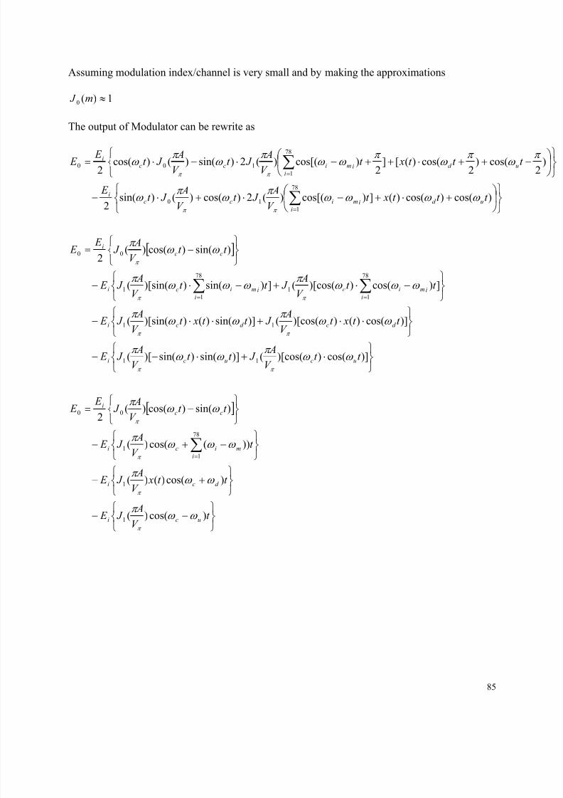
8/8/2019 Anthony Leung Thesis
http://slidepdf.com/reader/full/anthony-leung-thesis 94/116
85
Assuming modulation index/channel is very small and by making the approximations
1)(0 ≈m J
The output of Modulator can be rewrite as
[ ]
[ ]
−−
+−
−+−
−=
⋅+⋅−−
⋅⋅+⋅⋅−
−⋅+−⋅−
−=
+⋅+−⋅+⋅−
−++⋅++−⋅−⋅=
∑
∑ ∑
∑
∑
=
= =
=
=
t V
A J E
t t xV
A J E
t V
A J E
t t
V
A J
E E
t t V
A J t t
V
A J E
t t xt V
A J t t xt
V
A J E
t t V A J t t
V A J E
t t V
A J
E E
t t t xt V
A J t
V
A J t
E
t t t xt V
A J t
V
A J t
E E
uci
d ci
i
mici
cci
ucuci
d cd ci
i iimicimici
cci
ud
iimicc
i
i
ud imicci
)cos()(
)cos()()(
))(cos()(
)sin()cos()(
2
)]cos())[cos(()]sin()sin()[(
)]cos()())[cos(()]sin()())[sin((
])cos())[cos((])sin())[sin((
)sin()cos()(2
)cos()cos()(])cos[()(2)cos()()sin(2
cos()2
cos()([]2
)cos[()(2)sin()()cos(2
1
1
78
1
1
00
11
11
78
1
78
1
11
00
78
1
10
78
1
100
ω ω π
ω ω π
ω ω ω π
ω ω π
ω ω π
ω ω π
ω ω π
ω ω π
ω ω ω π ω ω ω π
ω ω π
ω ω ω ω π
ω π
ω
ω π
ω π
ω ω π
ω π
ω
π
π
π
π
π π
π π
π π
π
π π
π π
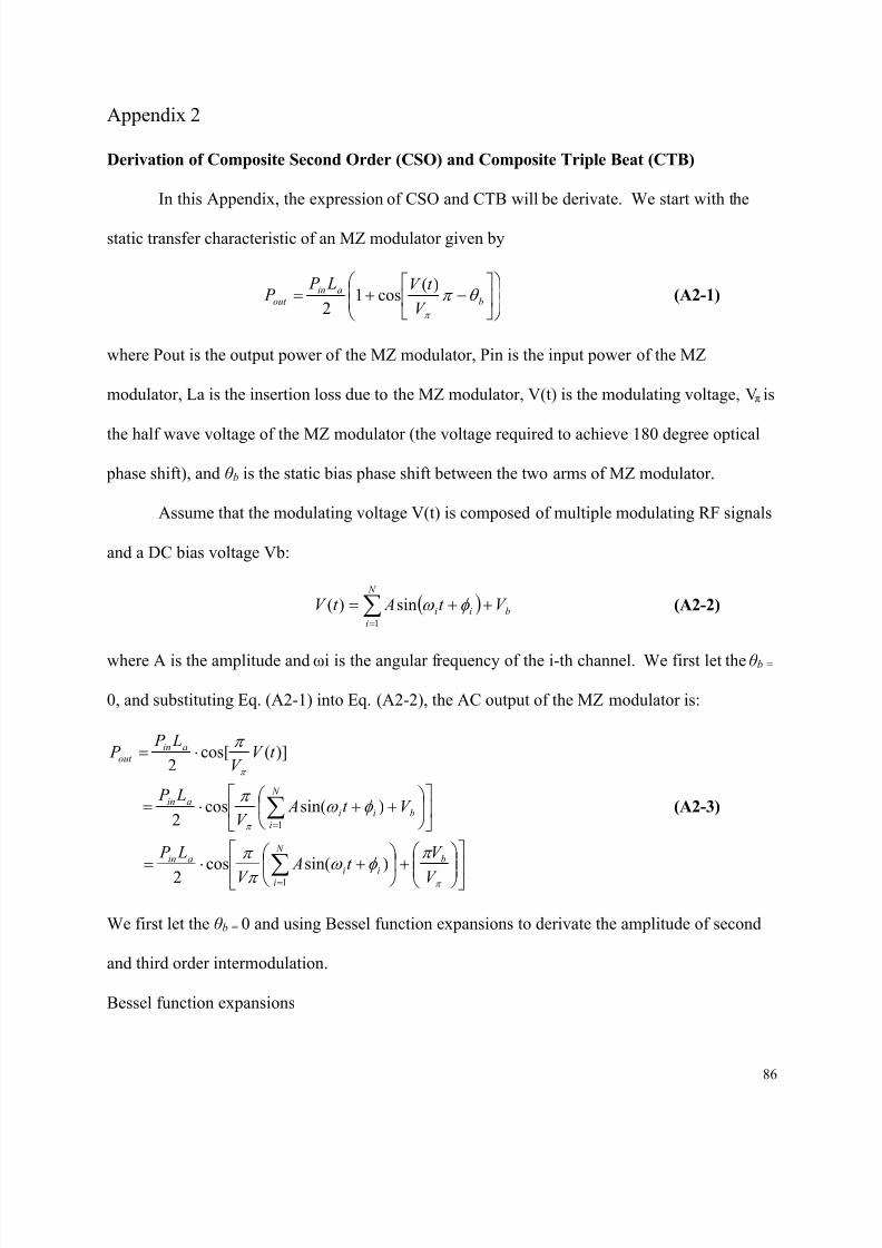
8/8/2019 Anthony Leung Thesis
http://slidepdf.com/reader/full/anthony-leung-thesis 95/116
86
Appendix 2
Derivation of Composite Second Order (CSO) and Composite Triple Beat (CTB)
In this Appendix, the expression of CSO and CTB will be derivate. We start with the
static transfer characteristic of an MZ modulator given by
−+= b
ainout
V
t V L P P θ π
π
)(cos1
2 (A2-1)
where Pout is the output power of the MZ modulator, Pin is the input power of the MZ
modulator, La is the insertion loss due to the MZ modulator, V(t) is the modulating voltage, Vπ is
the half wave voltage of the MZ modulator (the voltage required to achieve 180 degree optical
phase shift), and θ b is the static bias phase shift between the two arms of MZ modulator.
Assume that the modulating voltage V(t) is composed of multiple modulating RF signals
and a DC bias voltage Vb:
( ) b
N
i
ii V t At V ++= ∑=1
sin)( φ ω (A2-2)
where A is the amplitude and ωi is the angular frequency of the i-th channel. We first let the θ b =
0, and substituting Eq. (A2-1) into Eq. (A2-2), the AC output of the MZ modulator is:
+
+⋅=
++⋅=
⋅=
∑
∑
=
=
π
π
π
π φ ω
π
π
φ ω π
π
V
V t A
V
L P
V t AV
L P
t V V
L P P
b N
i ii
ain
N
i
biiain
ainout
1
1
)sin(cos2
)sin(cos2
)](cos[2
(A2-3)
We first let the θ b = 0 and using Bessel function expansions to derivate the amplitude of second
and third order intermodulation.
Bessel function expansions
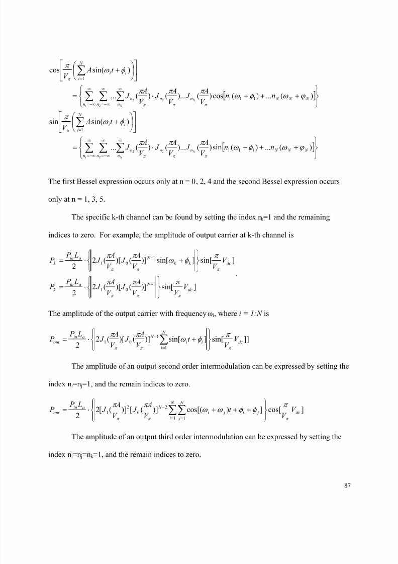
8/8/2019 Anthony Leung Thesis
http://slidepdf.com/reader/full/anthony-leung-thesis 96/116
87
[ ]
[ ]
+++⋅=
+
+++⋅=
+
∑ ∑ ∑
∑
∑ ∑ ∑
∑
∞
−∞=
∞
−∞=
∞
=
∞
−∞=
∞
−∞=
∞
=
i N
N
i N
N
n n n
N N N nnn
N
i
ii
n n n N N N nnn
N
i
ii
nnV
A J
V
A J
V
A J
t AV
nnV
A
J V
A
J V
A
J
t AV
2
22
2
22
)(...)(sin)()...()(...
)sin(sin
)(...)(cos)()...()(...
)sin(cos
111
1
111
1
ϕ ω φ ω π π π
φ ω π
ϕ ω φ ω
π π π
φ ω π
π π π
π
π π π
π
The first Bessel expression occurs only at n = 0, 2, 4 and the second Bessel expression occurs
only at n = 1, 3, 5.
The specific k-th channel can be found by setting the index nk =1 and the remaining
indices to zero. For example, the amplitude of output carrier at k-th channel is
]sin[)]()[(2
2
]sin[]sin[)]()[(22
1
01
1
01
dc
N aink
dck k
N aink
V
V V
A J
V
A J
L P P
V V V
A J
V
A J
L P P
π π π
π π π
π π π
π φ ω
π π
⋅=
+⋅=
−
−
.
The amplitude of the output carrier with frequency ωi, where i = 1:N is
]]sin[]sin[)]()[(22 1
1
01 dc
N
i
ii
N ainout V
V t
V
A J
V
A J
L P P
π π π
π φ ω
π π
+⋅= ∑=
−
The amplitude of an output second order intermodulation can be expressed by setting the
index ni=n j=1, and the remain indices to zero.
]cos[])cos[()]([)]([22 1 1
2
0
2
1 dc
N
i
N
j
ji ji
N ainout V
V t
V
A J
V
A J
L P P
π π π
π φ φ ω ω
π π
+++⋅= ∑∑= =
−
The amplitude of an output third order intermodulation can be expressed by setting the
index ni=n j=nk =1, and the remain indices to zero.

8/8/2019 Anthony Leung Thesis
http://slidepdf.com/reader/full/anthony-leung-thesis 97/116
88
]]sin[])sin[()]([)]([22 1 1 1
3
0
3
1 dc
N
i
N
j
N
k
k jik ji
N ainout V
V t
V
A J
V
A J
L P P
π π π
π φ φ φ ω ω ω
π π
+++++⋅= ∑∑∑= = =
−
Therefore, the power ratio of CSO to carrier is given by
2
2
1
01
2
0
2
1
)sin(
)cos(
)]()[(2
)]([)]([2
dc
dc
CSO N
N
V V
V V
N
V
A J
V
A J
V
A J
V
A J
C
CSO
π
π
π π
π π
π
π
π π
π π
⋅
=−
−
where Ncso is the product-count of CSO. The power ratio of CTB to carrier is given by
2
2
1
01
3
0
3
1
)sin(
)sin(
)]()[(2
)]([)]([2
dc
dc
CTB N
N
V V
V V
N
V
A J
V
A J
V
A J
V
A J
C
CTB
π
π
π π
π π
π
π
π π
π π
⋅
= −
−
where NCTB is the product-count of CTB.
It is clearly show that when the applied dc Voltage, Vdc, is set to ...),2
3,
2
1(, ±±=mmV π , the
CSO distortion null out. In other word, by setting the applied dc Voltage set to2
π V , the
modulator is biased at quadrature point, which cancel even-order distortion, and the bias phase
shift between the two arms of modulator is2
π .
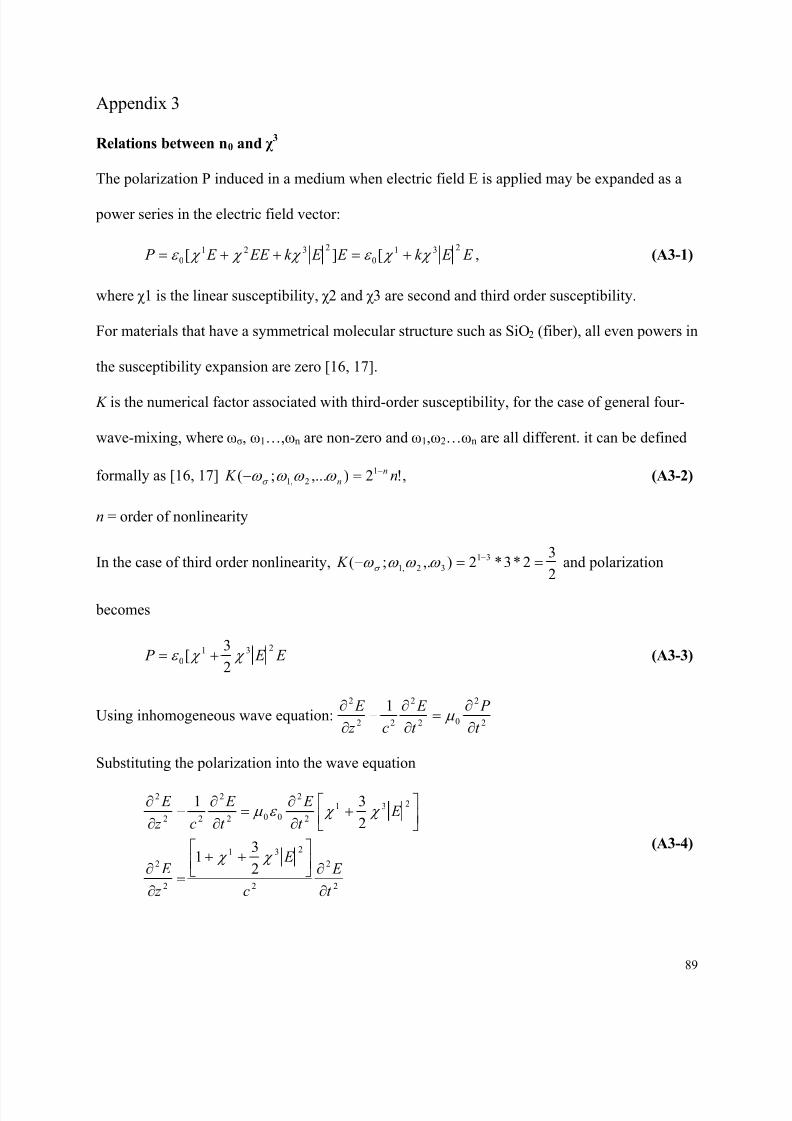
8/8/2019 Anthony Leung Thesis
http://slidepdf.com/reader/full/anthony-leung-thesis 98/116
89
Appendix 3
Relations between n0 and χ 3
The polarization P induced in a medium when electric field E is applied may be expanded as a
power series in the electric field vector:
E E k E E k EE E P 231
0
2321
0 [][ χ χ ε χ χ χ ε +=++= , (A3-1)
where χ 1 is the linear susceptibility, χ 2 and χ 3 are second and third order susceptibility.
For materials that have a symmetrical molecular structure such as SiO2 (fiber), all even powers in
the susceptibility expansion are zero [16, 17].
K is the numerical factor associated with third-order susceptibility, for the case of general four-
wave-mixing, where ωσ, ω1…,ωn are non-zero and ω1,ω2…ωn are all different. it can be defined
formally as [16, 17] !2),...;( 1
2,1 n K n
n
−=− ω ω ω ω σ , (A3-2)
n = order of nonlinearity
In the case of third order nonlinearity,2
32*3*2),.;( 31
32,1 ==− −ω ω ω ω σ K and polarization
becomes
E E P 231
02
3[ χ χ ε += (A3-3)
Using inhomogeneous wave equation:2
2
02
2
22
2 1
t
P
t
E
c z
E
∂
∂=
∂
∂−
∂
∂µ
Substituting the polarization into the wave equation
2
2
2
231
2
2
231
2
2
002
2
22
2
2
31
2
31
t
E
c
E
z
E
E t
E
t
E
c z
E
∂
∂
++
=∂
∂
+
∂
∂=
∂
∂−
∂
∂
χ χ
χ χ ε µ
(A3-4)
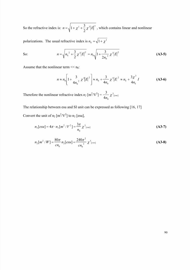
8/8/2019 Anthony Leung Thesis
http://slidepdf.com/reader/full/anthony-leung-thesis 99/116
90
So the refractive index is:231
2
31 E n χ χ ++= , which contains linear and nonlinear
polarizations. The usual refractive index is 1
0 1 χ +=n
So:23
2
0
0
232
02
31
2
3 E
nn E nn χ χ +=+= (A3-5)
Assume that the nonlinear term << n0:
I n
n E n
n E n
nn0
3
0
23
0
0
23
2
0
04
3
4
3
4
31
χ χ χ +≈+≈
+≈ (A3-6)
Therefore the nonlinear refractive index n2 [m2/V2] = ][3
04
3esu
n χ
The relationship between esu and SI unit can be expressed as following [16, 17]
Convert the unit of n2 [m2/V
2] to n2 [esu],
][3
0
22
22
3]/[4][ esu
nV mnesun χ
π π =⋅= (A3-7)
][32
0
2
2
0
22
240][
80]/[ esu
cnesuncnW mn χ
π π
== (A3-8)

8/8/2019 Anthony Leung Thesis
http://slidepdf.com/reader/full/anthony-leung-thesis 100/116
91
Appendix 4 Matlab Program
%Program 1: Nonlinear Distortion
%Plot Figure 2-2 to 2-4
clear all;
close all;index=0;index1=0;index2=0;index3=0;index4=0;%CTB Product Countschannel=[2:79]for N=78;
for r=channel;index1=index1+1;D(index1)=((r./2)*(N-r+1))+((1/4)*((N-3)^2-5-(0.5.*(1-(-1)^N))*(-
1)^(N+r)));
endend
%CATV IF carrierrun c:\eecs891\ber_cnr_pwr\channel_freq.m;
d=6;%CSO (fa-fb) Product Countschannel1=[2:79]for N=78;
for r=channel1;index2=index2+1;
D1(index2)=(N-1)*(1-((ch_freq(r-1)-d)./(ch_freq(78)-ch_freq(1))));end
end%CSO (fa+fb) Product Counts
channel2=[2:79]for N=78;
for r=channel2;index3=index3+1;
D2(index3)=(N-1)*((ch_freq(r-1)-2*ch_freq(1)+d)./(2*(ch_freq(78)-ch_freq(1))));
endend figure(1)plot(D);grid;hold;
[Nctb,ch]=max(D);plot(ch,Nctb,'*r');title('Figure 2-3 Third order product count vs. Channel Number)')xlabel('Channel Number')ylabel('Number of Terms')
figure(2)plot(D1,'.-r');grid;hold;plot(D2,'o-b');title('Figure 2-2 Second order product count vs. Channel Number)')
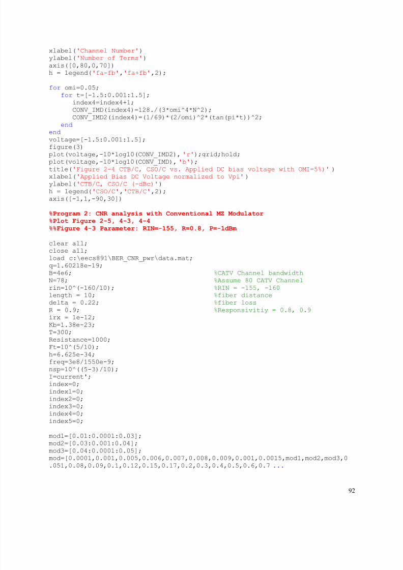
8/8/2019 Anthony Leung Thesis
http://slidepdf.com/reader/full/anthony-leung-thesis 101/116
92
xlabel('Channel Number')ylabel('Number of Terms')axis([0,80,0,70])h = legend('fa-fb','fa+fb',2);
for omi=0.05;for t=[-1.5:0.001:1.5];
index4=index4+1;CONV_IMD(index4)=128./(3*omi^4*N^2);CONV_IMD2(index4)=(1/69)*(2/omi)^2*(tan(pi*t))^2;
endendvoltage=[-1.5:0.001:1.5];figure(3)plot(voltage,-10*log10(CONV_IMD2),'r');grid;hold;plot(voltage,-10*log10(CONV_IMD),'b');title('Figure 2-4 CTB/C, CSO/C vs. Applied DC bias voltage with OMI=5%)')xlabel('Applied Bias DC Voltage normalized to Vpi')ylabel('CTB/C, CSO/C (-dBc)')h = legend('CSO/C','CTB/C',2);
axis([-1,1,-90,30])
%Program 2: CNR analysis with Conventional MZ Modulator
%Plot Figure 2-5, 4-3, 4-4
%%Figure 4-3 Parameter: RIN=-155, R=0.8, P=-1dBm
clear all;close all;load c:\eecs891\BER_CNR_pwr\data.mat;q=1.60218e-19;B=4e6; %CATV Channel bandwidthN=78; %Assume 80 CATV Channelrin=10^(-160/10); %RIN = -155, -160length = 10; %fiber distancedelta = 0.22; %fiber lossR = 0.9; %Responsivitiy = 0.8, 0.9irx = 1e-12;Kb=1.38e-23;T=300;Resistance=1000;Ft=10^(5/10);h=6.625e-34;freq=3e8/1550e-9;nsp=10^((5-3)/10);I=current';index=0;index1=0;
index2=0;index3=0;index4=0;index5=0;
mod1=[0.01:0.0001:0.03];mod2=[0.03:0.001:0.04];mod3=[0.04:0.0001:0.05];mod=[0.0001,0.001,0.005,0.006,0.007,0.008,0.009,0.001,0.0015,mod1,mod2,mod3,0.051,0.08,0.09,0.1,0.12,0.15,0.17,0.2,0.3,0.4,0.5,0.6,0.7...
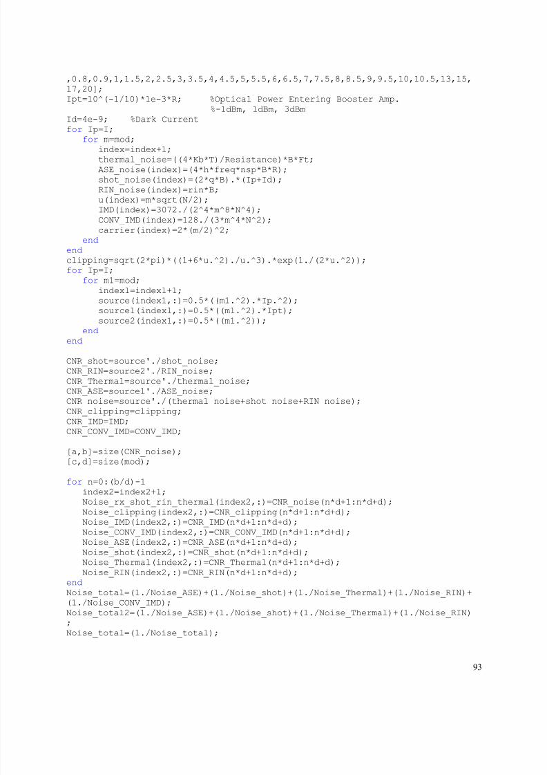
8/8/2019 Anthony Leung Thesis
http://slidepdf.com/reader/full/anthony-leung-thesis 102/116
93
,0.8,0.9,1,1.5,2,2.5,3,3.5,4,4.5,5,5.5,6,6.5,7,7.5,8,8.5,9,9.5,10,10.5,13,15,17,20];Ipt=10^(-1/10)*1e-3*R; %Optical Power Entering Booster Amp.
%-1dBm, 1dBm, 3dBmId=4e-9; %Dark Currentfor Ip=I;
for m=mod;index=index+1;thermal_noise=((4*Kb*T)/Resistance)*B*Ft;ASE_noise(index)=(4*h*freq*nsp*B*R);shot_noise(index)=(2*q*B).*(Ip+Id);RIN_noise(index)=rin*B;u(index)=m*sqrt(N/2);IMD(index)=3072./(2^4*m^8*N^4);CONV_IMD(index)=128./(3*m^4*N^2);carrier(index)=2*(m/2)^2;
endend clipping=sqrt(2*pi)*((1+6*u.^2)./u.^3).*exp(1./(2*u.^2));
for Ip=I;for m1=mod;
index1=index1+1;source(index1,:)=0.5*((m1.^2).*Ip.^2);source1(index1,:)=0.5*((m1.^2).*Ipt);source2(index1,:)=0.5*((m1.^2));
endend
CNR_shot=source'./shot_noise;CNR_RIN=source2'./RIN_noise;CNR_Thermal=source'./thermal_noise;CNR_ASE=source1'./ASE_noise;CNR_noise=source'./(thermal_noise+shot_noise+RIN_noise);CNR_clipping=clipping;CNR_IMD=IMD;CNR_CONV_IMD=CONV_IMD;
[a,b]=size(CNR_noise);[c,d]=size(mod);
for n=0:(b/d)-1index2=index2+1;Noise_rx_shot_rin_thermal(index2,:)=CNR_noise(n*d+1:n*d+d);Noise_clipping(index2,:)=CNR_clipping(n*d+1:n*d+d);Noise_IMD(index2,:)=CNR_IMD(n*d+1:n*d+d);Noise_CONV_IMD(index2,:)=CNR_CONV_IMD(n*d+1:n*d+d);
Noise_ASE(index2,:)=CNR_ASE(n*d+1:n*d+d);Noise_shot(index2,:)=CNR_shot(n*d+1:n*d+d);Noise_Thermal(index2,:)=CNR_Thermal(n*d+1:n*d+d);Noise_RIN(index2,:)=CNR_RIN(n*d+1:n*d+d);
end Noise_total=(1./Noise_ASE)+(1./Noise_shot)+(1./Noise_Thermal)+(1./Noise_RIN)+(1./Noise_CONV_IMD);Noise_total2=(1./Noise_ASE)+(1./Noise_shot)+(1./Noise_Thermal)+(1./Noise_RIN);Noise_total=(1./Noise_total);
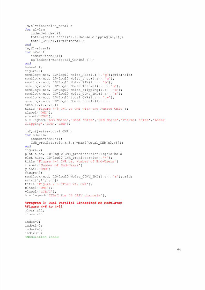
8/8/2019 Anthony Leung Thesis
http://slidepdf.com/reader/full/anthony-leung-thesis 103/116
94
[m,n]=size(Noise_total);for n1=1:m
index3=index3+1;total=[Noise_total(n1,:);Noise_clipping(n1,:)];total_CNR(n1,:)=min(total);
end [e,f]=size(I)for n2=1:f
index4=index4+1;DR(index4)=max(total_CNR(n2,:));
endhubs=1:f;figure(1)semilogx(mod, 10*log10(Noise_ASE(1,:)),'g');grid;hold;semilogx(mod, 10*log10(Noise_shot(1,:)),'c');semilogx(mod, 10*log10(Noise_RIN(1,:)),'b');semilogx(mod, 10*log10(Noise_Thermal(1,:)),'m');semilogx(mod, 10*log10(Noise_clipping(1,:)),'k');semilogx(mod, 10*log10(Noise_CONV_IMD(1,:)),'r');semilogx(mod, 10*log10(total_CNR(1,:)),'.-');
semilogx(mod, 10*log10(Noise_total2(1,:)));axis([0,10,0,80])title('Figure 4-3 CNR vs OMI with one Remote Unit');xlabel('OMI');ylabel('CNR');h = legend('ASE Noise','Shot Noise','RIN Noise','Thermal Noise','LaserClipping','CTB','CNR');
[m2,n2]=size(total_CNR);for n3=1:m2
index5=index5+1;CNR_predistortion(n3,:)=max([total_CNR(n3,:)]);
end figure(2)plot(hubs, 10*log10(CNR_predistortion));grid;holdplot(hubs, 10*log10(CNR_predistortion),'*');title('Figure 4-4 CNR vs. Number of End-Users')xlabel('Number of End-Users')ylabel('CNR')figure(3)semilogx(mod, 10*log10(Noise_CONV_IMD(1,:)),'r');grid;axis([0,10,0,80])title('Figure 2-5 CTB/C vs. OMI');xlabel('OMI');ylabel('CTB/C');h = legend('CTB/C for 78 CATV channels');
%Program 3: Dual Parallel Linearized MZ Modulator%Figure 4-6 to 4-11
clear all;close all
index=0;index1=0;index2=0;index3=0;%Modulation Index
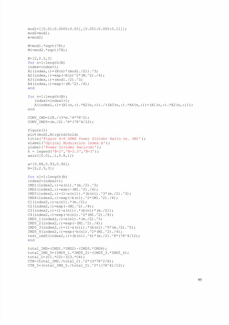
8/8/2019 Anthony Leung Thesis
http://slidepdf.com/reader/full/anthony-leung-thesis 104/116
95
mod1=[[0.01:0.0005:0.05],[0.051:0.005:0.11]];mod2=mod1;m=mod2;
M=mod1.*sqrt(78);M1=mod2.*sqrt(78);
B=[2,2.5,3]for n=1:length(B)index=index+1;A1(index,:)=(B(n)*(mod1./2)).^3;A2(index,:)=exp(-B(n)^2*(M.^2)./4);A3(index,:)=(mod1./2).^3;A4(index,:)=exp(-(M.^2)./4);end
for n=1:length(B);index1=index1+1;A(index1,:)=(A1(n,:).*A2(n,:))./((A3(n,:).*A4(n,:))+(A1(n,:).*A2(n,:)));
end
CONV_IMD=128./(3*m.^4*78^2);CONV_IMD5=(m./2).^8*(78^4/12);
figure(1)plot(mod1,A);grid;hold;title('Figure 4-6 DPMZ Power Divider Ratio vs. OMI');xlabel('Optical Modulation Index m');ylabel('Power Divider Ratio(A)');h = legend('B=2','B=2.5','B=3');axis([0.01,.1,0.8,1])
a=[0.88,0.93,0.96];b=[2,2.5,3];
for n1=1:length(b)index2=index2+1;IMD1(index2,:)=a(n1).*(m./2).^3;IMD2(index2,:)=exp(-(M1.^2)./4);IMD3(index2,:)=(1-a(n1)).*(b(n1).^3*(m./2).^3);IMD4(index2,:)=exp(-b(n1).^2*(M1.^2)./4);C1(index2,:)=a(n1).*(m./2);C2(index2,:)=exp(-(M1.^2)./4);C3(index2,:)=(1-a(n1)).*(b(n1)*(m./2));C4(index2,:)=exp(-b(n1).^2*(M1.^2)./4);IMD5_1(index2,:)=a(n1).*(m./2).^5;IMD5_2(index2,:)=exp(-(M1.^2)./4);
IMD5_3(index2,:)=(1-a(n1)).*(b(n1).^5*(m./2).^5);IMD5_4(index2,:)=exp(-b(n1).^2*(M1.^2)./4);test_imd5(index2,:)=(b(n1).^4)*(m./2).^8*(78^4/12);end
total_IMD=(IMD1.*IMD2)-(IMD3.*IMD4);total_IMD_5=(IMD5_1.*IMD5_2)-(IMD5_3.*IMD5_4);total_C=(C1.*C2)-(C3.*C4);CTB=(total_IMD./total_C).^2*(3*78^2/8);CTB_5=(total_IMD_5./total_C).^2*((78^4)/12);
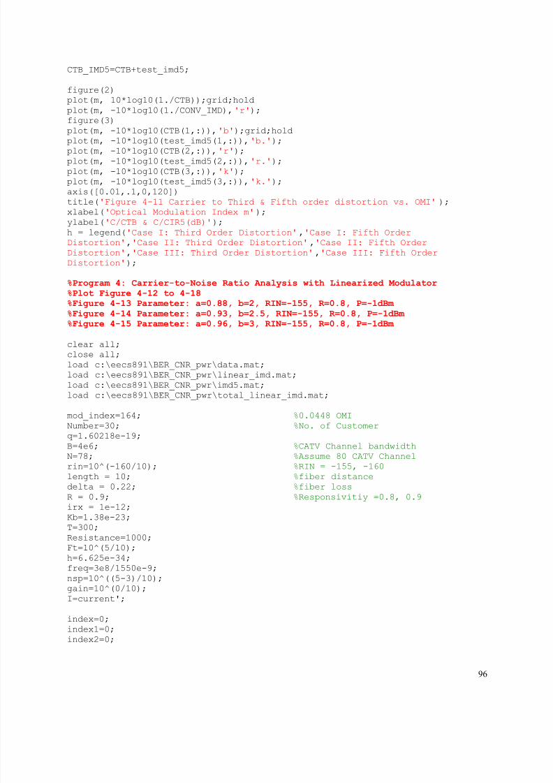
8/8/2019 Anthony Leung Thesis
http://slidepdf.com/reader/full/anthony-leung-thesis 105/116
96
CTB_IMD5=CTB+test_imd5;
figure(2)plot(m, 10*log10(1./CTB));grid;holdplot(m, -10*log10(1./CONV_IMD),'r');figure(3)plot(m, -10*log10(CTB(1,:)),'b');grid;holdplot(m, -10*log10(test_imd5(1,:)),'b.');plot(m, -10*log10(CTB(2,:)),'r');plot(m, -10*log10(test_imd5(2,:)),'r.');plot(m, -10*log10(CTB(3,:)),'k');plot(m, -10*log10(test_imd5(3,:)),'k.');axis([0.01,.1,0,120])title('Figure 4-11 Carrier to Third & Fifth order distortion vs. OMI');xlabel('Optical Modulation Index m');ylabel('C/CTB & C/CIR5(dB)');h = legend('Case I: Third Order Distortion','Case I: Fifth OrderDistortion','Case II: Third Order Distortion','Case II: Fifth OrderDistortion','Case III: Third Order Distortion','Case III: Fifth OrderDistortion');
%Program 4: Carrier-to-Noise Ratio Analysis with Linearized Modulator
%Plot Figure 4-12 to 4-18
%Figure 4-13 Parameter: a=0.88, b=2, RIN=-155, R=0.8, P=-1dBm
%Figure 4-14 Parameter: a=0.93, b=2.5, RIN=-155, R=0.8, P=-1dBm
%Figure 4-15 Parameter: a=0.96, b=3, RIN=-155, R=0.8, P=-1dBm
clear all;close all;load c:\eecs891\BER_CNR_pwr\data.mat;load c:\eecs891\BER_CNR_pwr\linear_imd.mat;load c:\eecs891\BER_CNR_pwr\imd5.mat;load c:\eecs891\BER_CNR_pwr\total_linear_imd.mat;
mod_index=164; %0.0448 OMINumber=30; %No. of Customerq=1.60218e-19;B=4e6; %CATV Channel bandwidthN=78; %Assume 80 CATV Channelrin=10^(-160/10); %RIN = -155, -160length = 10; %fiber distancedelta = 0.22; %fiber lossR = 0.9; %Responsivitiy =0.8, 0.9irx = 1e-12;Kb=1.38e-23;T=300;Resistance=1000;
Ft=10^(5/10);h=6.625e-34;freq=3e8/1550e-9;nsp=10^((5-3)/10);gain=10^(0/10);I=current';
index=0;index1=0;index2=0;
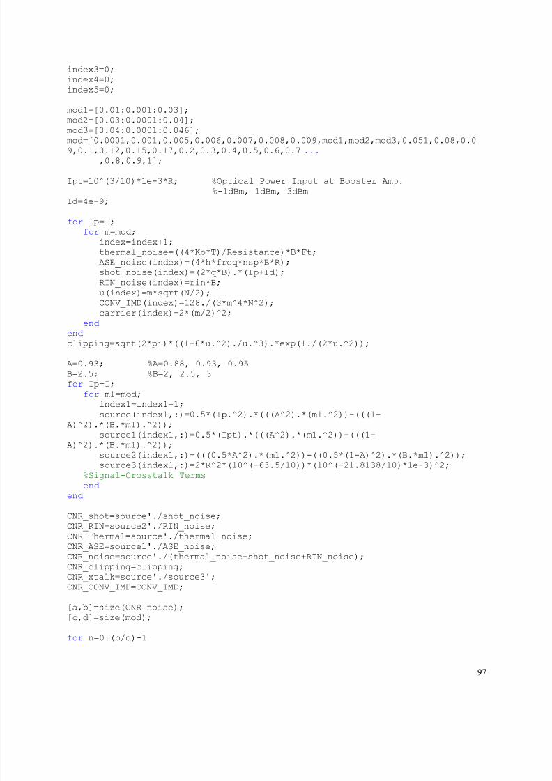
8/8/2019 Anthony Leung Thesis
http://slidepdf.com/reader/full/anthony-leung-thesis 106/116
97
index3=0;index4=0;index5=0;
mod1=[0.01:0.001:0.03];mod2=[0.03:0.0001:0.04];mod3=[0.04:0.0001:0.046];mod=[0.0001,0.001,0.005,0.006,0.007,0.008,0.009,mod1,mod2,mod3,0.051,0.08,0.09,0.1,0.12,0.15,0.17,0.2,0.3,0.4,0.5,0.6,0.7...
,0.8,0.9,1];
Ipt=10^(3/10)*1e-3*R; %Optical Power Input at Booster Amp.%-1dBm, 1dBm, 3dBm
Id=4e-9;
for Ip=I;for m=mod;
index=index+1;thermal_noise=((4*Kb*T)/Resistance)*B*Ft;ASE_noise(index)=(4*h*freq*nsp*B*R);
shot_noise(index)=(2*q*B).*(Ip+Id);RIN_noise(index)=rin*B;u(index)=m*sqrt(N/2);CONV_IMD(index)=128./(3*m^4*N^2);carrier(index)=2*(m/2)^2;
endendclipping=sqrt(2*pi)*((1+6*u.^2)./u.^3).*exp(1./(2*u.^2));
A=0.93; %A=0.88, 0.93, 0.95B=2.5; %B=2, 2.5, 3for Ip=I;
for m1=mod;index1=index1+1;source(index1,:)=0.5*(Ip.^2).*(((A^2).*(m1.^2))-(((1-
A)^2).*(B.*m1).^2));source1(index1,:)=0.5*(Ipt).*(((A^2).*(m1.^2))-(((1-
A)^2).*(B.*m1).^2));source2(index1,:)=(((0.5*A^2).*(m1.^2))-((0.5*(1-A)^2).*(B.*m1).^2));source3(index1,:)=2*R^2*(10^(-63.5/10))*(10^(-21.8138/10)*1e-3)^2;
%Signal-Crosstalk Termsend
end
CNR_shot=source'./shot_noise;CNR_RIN=source2'./RIN_noise;CNR_Thermal=source'./thermal_noise;
CNR_ASE=source1'./ASE_noise;CNR_noise=source'./(thermal_noise+shot_noise+RIN_noise);CNR_clipping=clipping;CNR_xtalk=source'./source3';CNR_CONV_IMD=CONV_IMD;
[a,b]=size(CNR_noise);[c,d]=size(mod);
for n=0:(b/d)-1
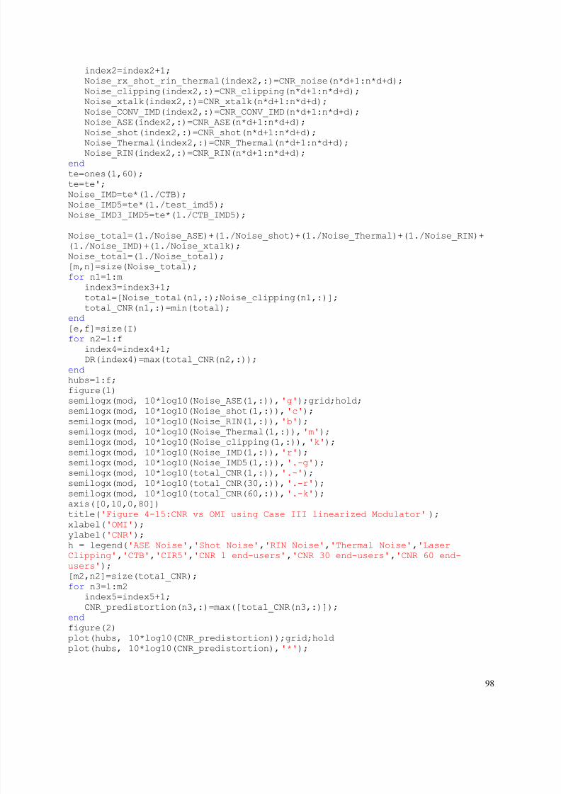
8/8/2019 Anthony Leung Thesis
http://slidepdf.com/reader/full/anthony-leung-thesis 107/116
98
index2=index2+1;Noise_rx_shot_rin_thermal(index2,:)=CNR_noise(n*d+1:n*d+d);Noise_clipping(index2,:)=CNR_clipping(n*d+1:n*d+d);Noise_xtalk(index2,:)=CNR_xtalk(n*d+1:n*d+d);Noise_CONV_IMD(index2,:)=CNR_CONV_IMD(n*d+1:n*d+d);Noise_ASE(index2,:)=CNR_ASE(n*d+1:n*d+d);Noise_shot(index2,:)=CNR_shot(n*d+1:n*d+d);Noise_Thermal(index2,:)=CNR_Thermal(n*d+1:n*d+d);Noise_RIN(index2,:)=CNR_RIN(n*d+1:n*d+d);
end te=ones(1,60);te=te';Noise_IMD=te*(1./CTB);Noise_IMD5=te*(1./test_imd5);Noise_IMD3_IMD5=te*(1./CTB_IMD5);
Noise_total=(1./Noise_ASE)+(1./Noise_shot)+(1./Noise_Thermal)+(1./Noise_RIN)+(1./Noise_IMD)+(1./Noise_xtalk);Noise_total=(1./Noise_total);[m,n]=size(Noise_total);
for n1=1:mindex3=index3+1;total=[Noise_total(n1,:);Noise_clipping(n1,:)];total_CNR(n1,:)=min(total);
end[e,f]=size(I)for n2=1:f
index4=index4+1;DR(index4)=max(total_CNR(n2,:));
endhubs=1:f;figure(1)semilogx(mod, 10*log10(Noise_ASE(1,:)),'g');grid;hold;semilogx(mod, 10*log10(Noise_shot(1,:)),'c');semilogx(mod, 10*log10(Noise_RIN(1,:)),'b');semilogx(mod, 10*log10(Noise_Thermal(1,:)),'m');semilogx(mod, 10*log10(Noise_clipping(1,:)),'k');semilogx(mod, 10*log10(Noise_IMD(1,:)),'r');semilogx(mod, 10*log10(Noise_IMD5(1,:)),'.-g');semilogx(mod, 10*log10(total_CNR(1,:)),'.-');semilogx(mod, 10*log10(total_CNR(30,:)),'.-r');semilogx(mod, 10*log10(total_CNR(60,:)),'.-k');axis([0,10,0,80])title('Figure 4-15:CNR vs OMI using Case III linearized Modulator');xlabel('OMI');ylabel('CNR');h = legend('ASE Noise','Shot Noise','RIN Noise','Thermal Noise','Laser
Clipping','CTB','CIR5','CNR 1 end-users','CNR 30 end-users','CNR 60 end-users');[m2,n2]=size(total_CNR);for n3=1:m2
index5=index5+1;CNR_predistortion(n3,:)=max([total_CNR(n3,:)]);
endfigure(2)plot(hubs, 10*log10(CNR_predistortion));grid;holdplot(hubs, 10*log10(CNR_predistortion),'*');
8/8/2019 Anthony Leung Thesis
http://slidepdf.com/reader/full/anthony-leung-thesis 108/116
99
title('CNR vs. Number of Remote Unit')xlabel('Number of Hubs (Remote Units) in a passive optical star network')ylabel('CNR')%Program 5: Q Value analysis with Linearized Modulator
%Plot figure 4-19 to 4-20
%Figure 4-19 Parameter: a=0.88, b=2, RIN=-155, R=0.8, P=-1dBm, Number=27
%Figure 4-14 Parameter: a=0.93, b=2.5, RIN=-155, R=0.8, P=-1dBm, Number=30
%Figure 4-15 Parameter: a=0.96, b=3, RIN=-155, R=0.8, P=-1dBm, Number=18
clear all;close all;load c:\eecs891\ber_cnr_pwr\data.mat;load c:\eecs891\ber_cnr_pwr\star_hub;Number=60;ix=164; %177, 164, 72q=1.60218e-19;B_total = 1e9; %Digital data rate is 1GbpsN=1; %1 digital ChannelBe=0.7*B_total/N; %Electrical Bandwidthlength = 10; %fiber distance
delta = 0.22; %fiber lossR = 0.9; %Responsivitiy= 0.8 & 0.9
Kb=1.38e-23;T=300;Resistance=1000;Ft=10^(5/10);h=6.625e-34;freq=3e8/1550e-9;F=5;nsp=10^((F-3)/10);rin=10^(-160/10); %RIN = -155 & -160Id=2e-9;
index=0;index1=0;index2=0;
mod1=[0.01:0.001:0.03];mod2=[0.03:0.0001:0.04];mod3=[0.04:0.0001:0.046];mod=[0.0001,0.001,0.005,0.006,0.007,0.008,0.009,mod1,mod2,mod3,0.051,0.08,0.09,0.1,0.12,0.15,0.17,0.2,0.3,0.4,0.5,0.6,0.7...
,0.8,0.9,1];
Ipt=sqrt(10^(3/10)*1e-3); %Input Optical Power at Booster%-1dBm, 1dBm & 3dBm
for Ip=current'*gain;for m=mod;index=index+1;thermal_noise=sqrt(((4*Be*Kb*T*Ft)/Resistance));%ASE_noise(index)=sqrt(4*R*Ip*nsp*freq*h*(gain)*Be);ASE_noise(index)=sqrt(4*nsp*freq*h*Be*R);shot_noise(index)= sqrt(2*q*Be*(Ip+Id));RIN_noise(index)=sqrt(Ip^2*rin*Be);
end
8/8/2019 Anthony Leung Thesis
http://slidepdf.com/reader/full/anthony-leung-thesis 109/116
100
end
A=0.93; %A=0.88, 0.93, 0.96B=2.5; %B=2, 2.5, 3
for Ip=current';for m1=mod;
index1=index1+1;source(index1,:)=(Ip).*((A.*m1*exp(-m1^2*80/4))-((1-A)*B.*m1*exp(-
B^2*m1^2*80/4)));source1(index1,:)=(Ipt).*((A.*m1*exp(-m1^2*80/4))-((1-A)*B.*m1*exp(-
B^2*m1^2*80/4)));source3(index1,:)=sqrt(2*R^2*(10^(-52.3845/10))*(10^(-21.8138/10)*1e-
3)^2);%Signal-Crosstalk Noise Term
end endpwr=source';
BPSK_Q_shot=source'./shot_noise;BPSK_Q_RIN=source'./RIN_noise;BPSK_Q_Thermal=source'./thermal_noise;BPSK_Q_ASE=source1'./ASE_noise;BPSK_Q_xtalk=source'./source3';BPSK_Q_noise=(1./BPSK_Q_ASE)+(1./BPSK_Q_shot)+(1./BPSK_Q_Thermal)+(1./BPSK_Q_RIN)+(1./BPSK_Q_xtalk);BPSK_Q_noise=(1./BPSK_Q_noise);BPSK_Q_noise_ASE=source1'./(ASE_noise);
[a,b]=size(BPSK_Q_noise);[c,d]=size(mod);
for n=0:(b/d)-1index2=index2+1;BPSK_Q(index2,:)=BPSK_Q_noise(n*d+1:n*d+d);ASK_Q(index2,:)=0.5*(BPSK_Q_noise(n*d+1:n*d+d));QPSK_Q(index2,:)=(1/sqrt(2))*(BPSK_Q_noise(n*d+1:n*d+d));BPSK_ASE(index2,:)=BPSK_Q_noise_ASE(n*d+1:n*d+d);power(index2,:)=pwr(n*d+1:n*d+d);
end
Q_Various=[BPSK_Q(Number,:); QPSK_Q(Number,:); ASK_Q(Number,:)];Q_ASE=[BPSK_ASE(Number,:);0.5*BPSK_ASE(Number,:);(1/sqrt(2))*BPSK_ASE(Number,:)];figure(1)
semilogx(mod, Q_Various);grid;title('Q Value at BPSK, QPSK & ASK Modulation vs Modulation Index')xlabel('Optical Modulation Index')ylabel('Q Value')axis([0.01,0.06,0,60])figure(2)plot(mod, Q_Various);gridtitle('Q Value at BPSK, QPSK & ASK Modulation vs. Modulation Index')xlabel('Optical Modulation Index')ylabel('Q')
8/8/2019 Anthony Leung Thesis
http://slidepdf.com/reader/full/anthony-leung-thesis 110/116
101
h = legend('BPSK','QPSK','ASK');axis([0,0.05,0,20])figure(3)plot(mod,Q_ASE);grid;hold;title('Q Value (Signal-ASE Noise only) Vs. Modulation Index')BPSK_value=BPSK_Q(Number,ix)QPSK_value=QPSK_Q(Number,ix)ASK_value=ASK_Q(Number,ix)p=10*log10((power(:,ix)./R)/1e-3);set=[BPSK_Q(:,ix),QPSK_Q(:,ix),ASK_Q(:,ix)];figure(4)subplot(2,1,1)plot(mod, Q_Various);gridaxis([0,0.05,0,20])title('Figure 4-20 "Set 2"')xlabel('OMI at 30 End-Users Optical Power Budget')ylabel('Q')h = legend('BPSK','QPSK','ASK');subplot(2,1,2)plot(p, set);grid;hold;
xlabel('Optical Channel Power at 4.34% OMI')ylabel('Q')h = legend('BPSK','QPSK','ASK');
%Program 6: FWM
%Plot figure 5-10A, 5-10B
run c:\eecs891\Crosstalk\SM_fiber_narrow_spacing;
clear all;close all;index=0;index1=0;index2=0;index3=0;index4=0;index5=0;
load c:\eecs891\Crosstalk\freq_spacing;load c:\eecs891\Crosstalk\smallwavelength;
wavelength=1550; %nmc=3e8/1e-9; %nm/sAeff =78*(1e-6)^2; %m^2delta =0.22/4.343; %/km = 0.25dB/kml=10; %kmleff=(1/delta)*(1-exp(-delta*l)); %kmD=(17e-12); %(Dispersion) s/(nm*km)
S=0.08e-12; %(Dispersion) s/(nm^2*km)n2=2.68e-20; %(non-linear refractive index)m^2/Wn=1.4645; %SM fiber refractive indexdf=df*1e6; %Convert MHz to HzP1=10^(-0.77/10)*1e-3;Ip=P1*0.9;a=0.93;b=2.5;m1=0.0434;
8/8/2019 Anthony Leung Thesis
http://slidepdf.com/reader/full/anthony-leung-thesis 111/116
102
source=(Ip)*((a*m1*exp(-m1^2*80/4))-((1-a)*b*m1*exp(-b^2*m1^2*80/4)));P=source/0.9%Receiver Optical Power per channelsave('power','P');B=((2*pi*wavelength^2)/c)*df.^2*D+((2*pi*wavelength^4)/c^2)*df.^3*S;N1=delta^2./(delta.^2+B.^2);N2=4*exp(-delta*l)*sin(B*l/2).^2;N3=(1-exp(-delta*l)).^2;N=N1.*(1+(N2./N3));
FWM=(32*pi*n2*(leff*1000)*6)/(240*(wavelength*1e-9)*Aeff);FWM1_sm=(FWM*P)^2*N;
figure(1)plot(dw, 10*log10(FWM1_sm));gridFWM2_sm=(FWM*P)^2*N*P*exp(-delta*l);
figure(2)subplot(2,1,1)plot(dw, 10*log10(FWM2_sm/1e-3));grid
title('Figure 5-10A FWM optical power(dBm) vs. Wavelength Separation(nm)')ylabel('FWM optical power (dBm)')subplot(2,1,2)plot(dw, 10*log10(FWM1_sm));gridtitle('Figure 5-10B Ratio of FWM power to transmitted ch. power vs.Wavelength Separation(nm)')xlabel('Wavelength Separation(nm)')ylabel('FWM crosstalk level')save('fwm_sm_ratio','FWM1_sm');save('fwm_sm_power','FWM2_sm');
%Program 7: SRS,XPM+FWM
%Plot Figure 5-7,5-8,5-9A&B,5-11 & 5-12
run c:\eecs891\Crosstalk\SM_fiber_narrow_spacing;clear all;close all;index=0;index1=0;index2=0;index3=0;index4=0;index5=0;index6=0;
load c:\eecs891\Crosstalk\smallgain;load c:\eecs891\Crosstalk\smallwavelength;load c:\eecs891\ber_cnr_pwr\data.mat;
load c:\eecs891\crosstalk\freq_spacing;
[m,number]=size(gain);
p=1 %effective polarization%Note: If the polarizations of the two (2) fields are closed to perpendicular(p=0.00001). Crosstalk mininal.%Note: If the polarizations of the two (2) fields are parallel (p=1),Crosstalk mininal.
8/8/2019 Anthony Leung Thesis
http://slidepdf.com/reader/full/anthony-leung-thesis 112/116
103
Aeff = 78*(1e-6)^2; %m^2Aeff1=78*(1e-6)^2; %m^2delta =0.222/4.343; %/km = 0.25dB/km l=10; %kmleff=(1/delta)*(1-exp(-delta*l));Dispersion=(17e-12); %s/nm/kmDispersion1=17 ; %ps/nm/kmP1=10^(-0.77/10)*1e-3;Ip=P1*0.9;
a=0.93;b=2.5;m1=0.0434;source=(Ip)*((a*m1*exp(-m1^2*80/4))-((1-a)*b*m1*exp(-b^2*m1^2*80/4)));P=source/0.9; %Optical Power per Channel
d=Dispersion*(dw);
freq=[0:.01:6];freq=freq*1e6;
for n=1:number%%%%%%%%%%%%%index=index+1;%%%%%%%%%%%%%
A(index,:)=((p*gain(n).*P)/(Aeff/1000)).^2; %1/km^2B(index,:)=1+exp(-2*delta*l)-2*exp(-delta*l).*cos(2*pi*freq*d(n)*l);C(index,:)=(delta)^2+(2*pi*freq*d(n)).^2; %1/km^2 D(index,:)=(1+((p*gain(n)*P*leff*1000)/Aeff1)).^2;srs(index,:)=(A(n,:)).*(B(n,:)./(C(n,:)));end
n2=2.68e-20 ; %m^2/W wavelength=1550; %nmwavelength=wavelength*(1e-9/1000); %convert to kmwavelength1=1550 ; %nm
c=3e8 ; %m/sc=3e8*(1e-12/1e-9); %convert to ps/nm b2=-((wavelength1)^2/(2*pi*c))*Dispersion1; %ps^2/km
alpha=2*pi*n2/(wavelength*Aeff1); %1/km
dt=dw*Dispersion1;
for n1=1:number%%%%%%%%%%%%%%%%%%
index1=index1+1;%%%%%%%%%%%%%%%%%%
A1(index1,:)=2*alpha*P;B1(index1,:)=exp(i*b2*(2*pi*freq*1e-12).^2*l*1/2)-exp(-delta*l+i*(2*pi*freq*1e-12).*dt(n1)*l);B2(index1,:)=i.*(delta-i.*2*pi*freq*1e-12.*dt(n1)+(i.*b2*(2*pi*freq*1e-12).^2*0.5));C1(index1,:)=exp(-i*b2*(2*pi*freq*1e-12).^2*l*1/2)-exp(-delta*l+i*(2*pi*freq*1e-12).*dt(n1)*l);
8/8/2019 Anthony Leung Thesis
http://slidepdf.com/reader/full/anthony-leung-thesis 113/116
104
C2(index1,:)=i.*(delta-i.*2*pi*freq*1e-12.*dt(n1)-(i.*b2*(2*pi*freq*1e-12).^2*0.5));xpm(index1,:)=abs(A1(n1,:).*((B1(n1,:)./B2(n1,:))-(C1(n1,:)./C2(n1,:)))).^2;end
xtalk_srs_xpm=abs(((srs)+(xpm)));xtalk_srs_xpm1=abs(((srs)-(xpm)));srs_6MHz=(P^2/freq(length(freq))).*srs;
%%%%%%%%%%%%%%%%%%%%%%%%%%%%%%%%%%%%%%%%%%%%%%%%%%%%%%%%%%%%%%%%%%%example:%The modulation frequency is 1GHz%The bandwidth_range is 0.1GHz%The count will be starting at%0Hz, 0.1GHz,0.2GHz,0.3GHz....0.9GHz%srs_6MHz(1), srs_6MHz(1000+1),srs_6MHz(2000+1)...srs_6MHz(9000+1)%%%%%%%%%%%%%%%%%%%%%%%%%%%%%%%%%%%%%%%%%%%%%%%%%%%%%%%%%%%%%%%%%%% n2=1modulation_frequency=freq(length(freq)); %modulation frequency bandwidth,6MHz
%count=modulation_frequency/((length(freq)-1)/n); bandwidth_range=n2*1e6 %if n2=1, bandwidth_range is 1e6
%if n2=0.01, bandwidth range is 10000Hzcount=(length(freq)-1)/(modulation_frequency/bandwidth_range);
for number1=1:numberfor number2=0:(modulation_frequency/bandwidth_range)-1
%%%%%%%%%%%%%%%%%%%%index3=index3+1;%%%%%%%%%%%%%%%%%%%%
srs_6MHz_total(number1,index3)=srs_6MHz(number1,(count*number2+1))*bandwidth_range;
endend
for number3=1:number%%%%%%%%%%%%%%%%% index4=index4+1;%%%%%%%%%%%%%%%%%%srs_total(index4)=sum(srs_6MHz_total(index4,:));
end
xpm_6MHz=(P^2/freq(length(freq))).*xpm;
for number4=1:numberfor number5=0:(modulation_frequency/bandwidth_range)-1
%%%%%%%%%%%%%%%%%%index5=index5+1;%%%%%%%%%%%%%%%%%%
xpm_6MHz_total(number4,index5)=xpm_6MHz(number4,(count*number5+1))*bandwidth_range;
endend
for number6=1:number

8/8/2019 Anthony Leung Thesis
http://slidepdf.com/reader/full/anthony-leung-thesis 114/116
105
%%%%%%%%%%%%%%%% index6=index6+1%%%%%%%%%%%%%%%%xpm_total(index6)=sum(xpm_6MHz_total(index6,:));
end
xtalk_srs_xpm_6MHz=abs((srs_total+xpm_total));
figure(1)plot(freq,10*log10((srs)));grid;title('Crosstalk (SRS) vs. Modulation Frequency')xlabel('Modulation Freqency (Hz)')ylabel('Crosstalk (SRS)')figure(2)plot(freq, 10*log10(xpm),'.-');gridtitle('Crosstalk (XPM) vs. Modulation Frequency')xlabel('Modulation Freqency (Hz)')ylabel('Crosstalk (XPM)')figure(3)plot(freq,10*log10(xtalk_srs_xpm));grid
title('Figure 5-7 Crosstalk (SRS+XPM) vs. 6MHz Modulation Frequency')xlabel('Modulation Freqency (Hz)')ylabel('Crosstalk (SRS+XPM)')figure(4)plot(freq,10*log10(xtalk_srs_xpm1));title('Figure 5-8 Crosstalk (SRS+XPM) vs. 6MHz Modulation Frequency')xlabel('Modulation Freqency (Hz)')ylabel('Crosstalk (SRS,XPM)')figure(6)plot(dw,10*log10(srs_total/1e-3),'r');holdplot(dw,10*log10(xpm_total/1e-3),'g');plot(dw,10*log10(xtalk_srs_xpm_6MHz/1e-3),'.-');gridtitle('Crosstalk Electrical power (dBm) vs. Wavelength Separation (nm)')xlabel('Wavelength Separation(nm)')ylabel('Crosstalk (SRS,XPM& SRS+XPM)')h = legend('SRS','XPM','Crosstalk(SRS+XPM)',3);figure(7)subplot(2,1,1)plot(dw,10*log10(sqrt(srs_total)/1e-3),'r');holdplot(dw,10*log10(sqrt(xpm_total)/1e-3),'g');plot(dw,10*log10(sqrt(xtalk_srs_xpm_6MHz)/1e-3),'.');gridtitle('Figure 5-9A Xtalk Optical power(dBm) vs. Wavelength Separation(nm)')ylabel('Crosstalk Optical Power (dBm)')h = legend('SRS','XPM','Crosstalk(SRS+XPM)',3);subplot(2,1,2)plot(dw,10*log10(sqrt(srs_total)/(P)),'r');holdplot(dw,10*log10(sqrt(xpm_total)/(P)),'g');
plot(dw,10*log10(sqrt(xtalk_srs_xpm_6MHz)/(P)),'.');gridtitle('Figure 5-9B xtalk normalized to transmitted ch. power vs. WavelengthSeparation(nm)')xlabel('Wavelength Separation(nm)')ylabel('Crosstalk level (dB)')h = legend('SRS','XPM','Crosstalk(SRS+XPM)',3);
load c:\eecs891\crosstalk\fwm_sm_ratio;load c:\eecs891\crosstalk\fwm_sm_power;
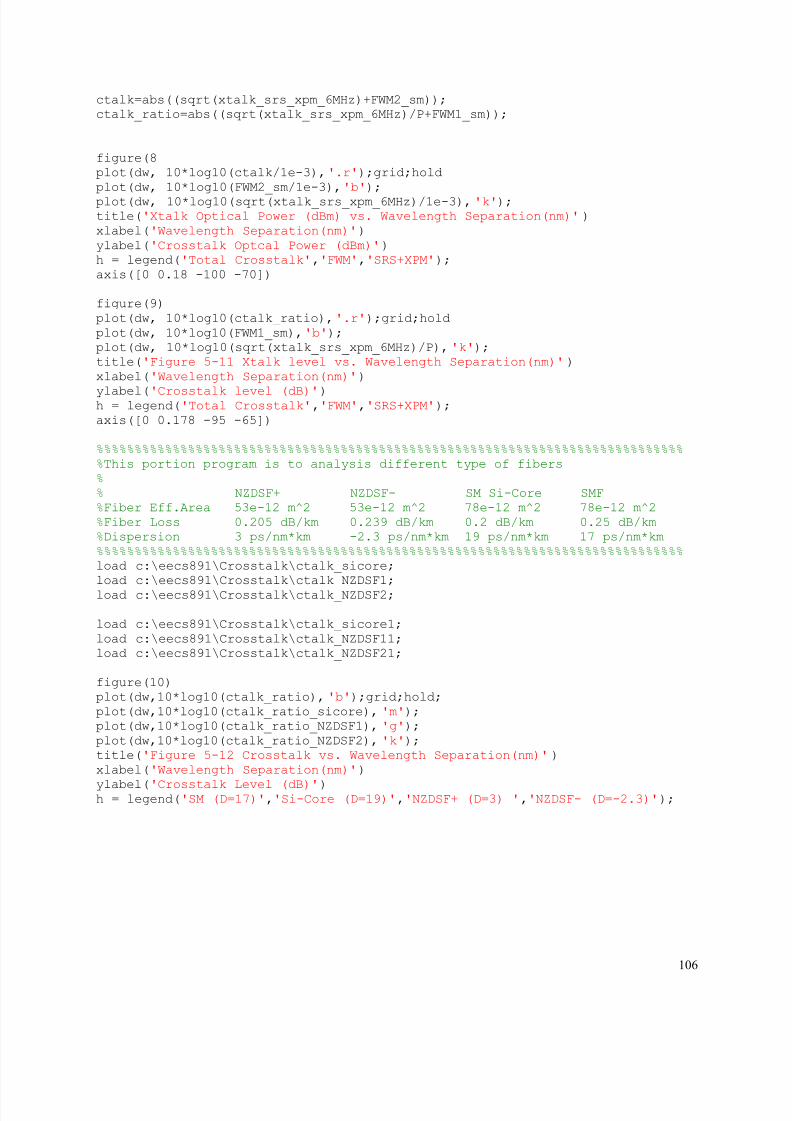
8/8/2019 Anthony Leung Thesis
http://slidepdf.com/reader/full/anthony-leung-thesis 115/116
106
ctalk=abs((sqrt(xtalk_srs_xpm_6MHz)+FWM2_sm));ctalk_ratio=abs((sqrt(xtalk_srs_xpm_6MHz)/P+FWM1_sm));
figure(8plot(dw, 10*log10(ctalk/1e-3),'.r');grid;holdplot(dw, 10*log10(FWM2_sm/1e-3),'b');plot(dw, 10*log10(sqrt(xtalk_srs_xpm_6MHz)/1e-3),'k');title('Xtalk Optical Power (dBm) vs. Wavelength Separation(nm)')xlabel('Wavelength Separation(nm)')ylabel('Crosstalk Optcal Power (dBm)')h = legend('Total Crosstalk','FWM','SRS+XPM');axis([0 0.18 -100 -70])
figure(9)plot(dw, 10*log10(ctalk_ratio),'.r');grid;holdplot(dw, 10*log10(FWM1_sm),'b');plot(dw, 10*log10(sqrt(xtalk_srs_xpm_6MHz)/P),'k');title('Figure 5-11 Xtalk level vs. Wavelength Separation(nm)')xlabel('Wavelength Separation(nm)')
ylabel('Crosstalk level (dB)')h = legend('Total Crosstalk','FWM','SRS+XPM');axis([0 0.178 -95 -65])
%%%%%%%%%%%%%%%%%%%%%%%%%%%%%%%%%%%%%%%%%%%%%%%%%%%%%%%%%%%%%%%%%%%%%%%%%%%%%%This portion program is to analysis different type of fibers%% NZDSF+ NZDSF- SM Si-Core SMF%Fiber Eff.Area 53e-12 m^2 53e-12 m^2 78e-12 m^2 78e-12 m^2%Fiber Loss 0.205 dB/km 0.239 dB/km 0.2 dB/km 0.25 dB/km%Dispersion 3 ps/nm*km -2.3 ps/nm*km 19 ps/nm*km 17 ps/nm*km%%%%%%%%%%%%%%%%%%%%%%%%%%%%%%%%%%%%%%%%%%%%%%%%%%%%%%%%%%%%%%%%%%%%%%%%%%%%%load c:\eecs891\Crosstalk\ctalk_sicore;load c:\eecs891\Crosstalk\ctalk_NZDSF1;load c:\eecs891\Crosstalk\ctalk_NZDSF2;
load c:\eecs891\Crosstalk\ctalk_sicore1;load c:\eecs891\Crosstalk\ctalk_NZDSF11;load c:\eecs891\Crosstalk\ctalk_NZDSF21;
figure(10)plot(dw,10*log10(ctalk_ratio),'b');grid;hold;plot(dw,10*log10(ctalk_ratio_sicore),'m');plot(dw,10*log10(ctalk_ratio_NZDSF1),'g');plot(dw,10*log10(ctalk_ratio_NZDSF2),'k');title('Figure 5-12 Crosstalk vs. Wavelength Separation(nm)')xlabel('Wavelength Separation(nm)')
ylabel('Crosstalk Level (dB)')h = legend('SM (D=17)','Si-Core (D=19)','NZDSF+ (D=3) ','NZDSF- (D=-2.3)');
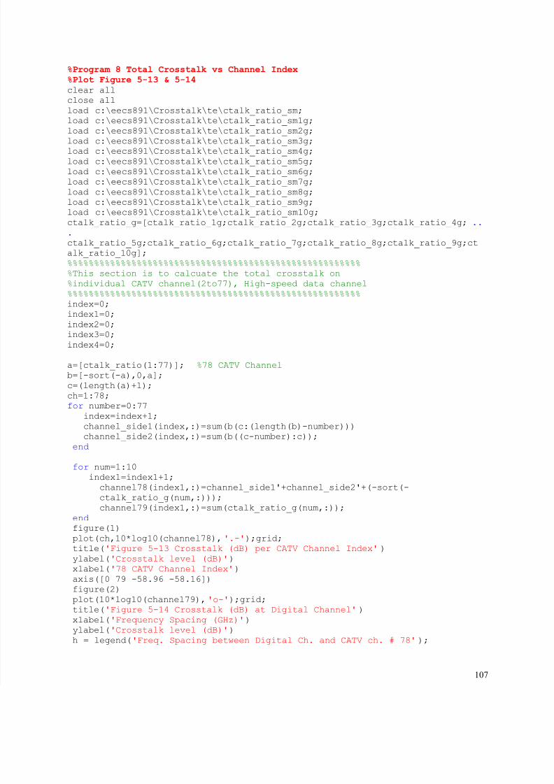
8/8/2019 Anthony Leung Thesis
http://slidepdf.com/reader/full/anthony-leung-thesis 116/116
%Program 8 Total Crosstalk vs Channel Index
%Plot Figure 5-13 & 5-14
clear allclose allload c:\eecs891\Crosstalk\te\ctalk_ratio_sm;load c:\eecs891\Crosstalk\te\ctalk_ratio_sm1g;load c:\eecs891\Crosstalk\te\ctalk_ratio_sm2g;load c:\eecs891\Crosstalk\te\ctalk_ratio_sm3g;load c:\eecs891\Crosstalk\te\ctalk_ratio_sm4g;load c:\eecs891\Crosstalk\te\ctalk_ratio_sm5g;load c:\eecs891\Crosstalk\te\ctalk_ratio_sm6g;load c:\eecs891\Crosstalk\te\ctalk_ratio_sm7g;load c:\eecs891\Crosstalk\te\ctalk_ratio_sm8g;load c:\eecs891\Crosstalk\te\ctalk_ratio_sm9g;load c:\eecs891\Crosstalk\te\ctalk_ratio_sm10g;ctalk_ratio_g=[ctalk_ratio_1g;ctalk_ratio_2g;ctalk_ratio_3g;ctalk_ratio_4g; ...ctalk_ratio_5g;ctalk_ratio_6g;ctalk_ratio_7g;ctalk_ratio_8g;ctalk_ratio_9g;ctalk_ratio_10g];%%%%%%%%%%%%%%%%%%%%%%%%%%%%%%%%%%%%%%%%%%%%%%%%%%%%%%%
%This section is to calcuate the total crosstalk on%individual CATV channel(2to77), High-speed data channel%%%%%%%%%%%%%%%%%%%%%%%%%%%%%%%%%%%%%%%%%%%%%%%%%%%%%%%index=0;index1=0;index2=0;index3=0;index4=0;
a=[ctalk_ratio(1:77)]; %78 CATV Channelb=[-sort(-a),0,a];c=(length(a)+1);ch=1:78;for number=0:77
index=index+1;channel_side1(index,:)=sum(b(c:(length(b)-number)))channel_side2(index,:)=sum(b((c-number):c));
end