Embed Size (px)
Citation preview
EE/CENG 464– Senior Design Spring 2016College of Engineering Prof. C.R. TolleSouth Dakota School of Mines & Technology
Anti-aliasing Filter Design Mini ProjectJan. 2016 Rev. 1
1 Project Definition
1.1 Project Overview
This document outlines a mini-design project required in EE/CENG-464. The goals for this project are outlined below in theproject requirement portion of the Reqs. & Specs. document, see attached in Appendix C Section 2.1. You will be requiredto design an anti-aliasing filter and its circuit, analyze the design within SPICE to ensure that your design meets the project’sdesign specs given in Appendix C Section 2.2, and lay out a small circuit board to implement the design. Once these stepsare complete, you are to write a short report detailing your design process, calculations, simulations, and lay outs. The fullset of projects requirements and specifications are documented in a requirements and specification documents attached inAppendix C.
2 Butterworth Filter Design Background
2.1 Butterworth Filter Design Equations
It is well known that a Butterworth filter achieves maximum flatness within the pass-band [1]. In this effort, we will assumethat maximum flatness within the pass-band achieves the requirement of minimal distortion within the pass-band, see Req.1 in Appendix C Section 2.1. Moreover, a Butterworth filter can be completely defined by three key parameters: cutofffrequency, fc, stop frequency, fs, and number of poles, N [2]. The basic derivations, results and equations that followhave been obtained/modified from the results in [2]. The number of poles, N , is a function of filter attenuation, δdB , at thestop-band frequency, fs, and cutoff frequency, fc:
N(δdB, fc, fs) =
log10
1
10
(2δdB20
) − 1
2 log10
(fsfc
) (1)
Once the number of poles has been specified, each of their locations can be calculated using the following formula:
sk = 2πfcej π2 ej
(2k+1)π2N where k = 0, 1, . . . , N − 1 (2)
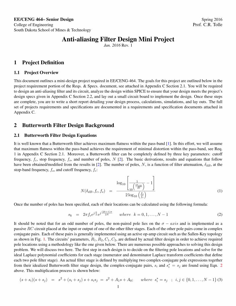
It should be noted that for an odd number of poles, the non-paired pole lies on the σ − axis and is implemented as apassiveRC circuit placed at the input or output of one of the other filter stages. Each of the other pole pairs come in complexconjugate pairs. Each of these pairs is generally implemented using an active op-amp circuit such as the Sallen-Key topologyas shown in Fig. 1. The circuits’ parameters, R1, R2, C1, C2, are defined by actual filter design in order to achieve requiredpole locations using a methodology like the one given below. There are numerous possible approaches to solving this designproblem. We will discuss two here. The first step in each design is to decide on the filtering pole locations and solve for theideal Laplace polynomial coefficients for each stage (numerator and denominator Laplace transform coefficients that defineeach two pole filter stage). An actual filter stage is defined by multiplying two complex-conjugate pole expressions togetherfrom their idealized Butterworth filter stage design, the complex-conjugate pairs, si and s∗i = sj are found using Eqn. 2above. This multiplication process is shown below:
(s+ si)(s+ sj) = s2 + (si + sj) s+ sisj = s2 +A1s+A0; where s∗i = sj ; i, j ∈ 0, 1, . . . , N − 1 (3)
1
Figure 1: Shown above is a two stage Sallen-Key op-amp circuit topology for two complex-conjugate pole pair fil-ter stages implementing a 1000Hz cuttoff frequency 4 pole Butterworth anti-alaising filter, additional backgroundinformation for this design can be obtained in [3] and [4].
The above target coefficients values, A1 and A0, can now be used to design our filter stages. Based on some simple circuitanalysis of the Sallen-Key circuit topology, one can obtain the following input-output Laplace transform expression:
voutvin
=1
R1R2C1C2
s2 + (R1+R2)R1R2C1
s+ 1R1R2C1C2
(4)
Setting our desired filter coefficients equal to the above denominator coefficients, A1 and A0, we obtain the following twoequations:
A1 =(R1 +R2)
R1R2C1(5)
A0 =1
R1R2C1C2(6)
Using best design practices, we should choose our capacitors first and then solve for our resistor values. However when wedo this, notice that our above equations become non-linear in resistance, namely they contain a ratio of unknowns: (R1+R2)
R1R2.
Thus we can’t use traditional linear techniques to solve these equations. We will introduce two approaches that can be usedto solve these types of non-linear problems: first, one can develop an iterative solution for the problem; second, since thisproblem is only second order, a simple quadratic solution restricting the design space to real values can be implemented.Both methods are discussed further below to help provide additional design techniques for your future use.
For this problem, we can construct an iterative solution by choosing our real capacitor values, C1 and C2 and thensetting up an iteration to estimate our resistor values based on our two constraint equations 5 and 6 above. We develop thisapproach next (more formal gradient decent methods can also be developed depending on the nature of the non-linearity andthe constraint equations). Choose an initial R2 value, calculate R1 and update R2 using the following equations:
R1 =1
A0R2C1C2(7)
R2 = R2 + η (A1R1R2C1 − (R1 +R2)) where η = .1, (8)
η is known as a learning factor. It controls the convergence rate of the learning iteration. Moreover, η helps reduce gradientovershoot within the learning process and provides for a smoother convergence to the desired value. An iterative method isa learning method. The usefulness of learning methods to solve non-linear problems is an important technique for a modernengineer to be aware of, thus we are introducing it within this mini project where it can be formally compared to other typesof solutions such as our next approach.
2
Our second, more straight forward approach to this second order problem is to use the quadratic equation, and restrict itssolution space to real numbers. For most non-linear problems an analytic solution does not exist, that is why this is a usefulexample problem. We can proceed by rearranging our constraint equations 5 and 6 as follows. First solve for R1R2 usingEqn. 6:
R1R2 =1
A0C1C2(9)
Next solve for R2 via Eqn. 5:
R2 =R1
A1R1C1 − 1(10)
Now we can obtain a quadratic equation in R1 by substituting Eqn. 10 into Eqn. 9 and rearranging terms:
R21
A1R1C1 − 1=
1
A0C1C2(11)
A0C1C2 R21 = A1C1 R1 − 1 (12)
R21 −
A1
A0C2R1 +
1
A0C1C2= 0 (13)
The above equation can be easily solved via the quadratic formula:
R1 =1
2
A1
A0C2±
√(A1
A0C2
)2
− 4
(1
A0C1C2
) (14)
Since we know that our resistances must be real valued, the term under the radical must be positive, which leads us to thefollowing constraint on our capacitors:(
A1
A0C2
)2
− 4
(1
A0C1C2
)≥ 0 (15)(
A1
A0C2
)2
≥ 4
(1
A0C1C2
)(16)
A21
A20C
22
≥ 4
(1
A0C1C2
)(17)
A21
A20
C1 ≥ 4
(C22
A0C2
)(18)
C1 ≥ 4
(A2
0
A21
C2
A0
)(19)
C1 ≥ 4 A0
A21
C2 (20)
So our second design method can proceed by choosing a realizable C1 and C2 that honor Eqn. 20. Then simply calculate ofR1 and R2 via Eqns. 14 and 10. One can then design a resistor network for R1 and R2 that achieves the desired accuracy forR1 and R2.
2.2 Butterworth Example Filter Design
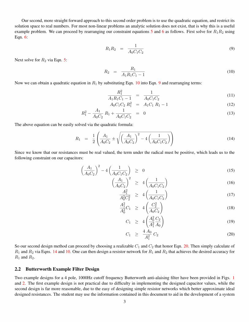
Two example designs for a 4 pole, 1000Hz cutoff frequency Butterworth anti-alaising filter have been provided in Figs. 1and 2. The first example design is not practical due to difficulty in implementing the designed capacitor values, while thesecond design is far more reasonable, due to the easy of designing simple resistor networks which better approximate idealdesigned resistances. The student may use the information contained in this document to aid in the development of a system
3
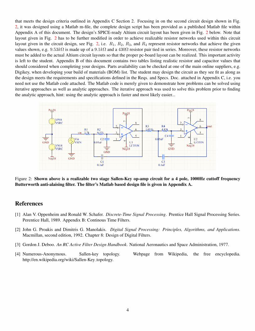
that meets the design criteria outlined in Appendix C Section 2. Focusing in on the second circuit design shown in Fig.2, it was designed using a Matlab m-file, the complete design script has been provided as a published Matlab file withinAppendix A of this document. The design’s SPICE-ready Altium circuit layout has been given in Fig. 2 below. Note thatlayout given in Fig. 2 has to be further modified in order to achieve realizable resistor networks used within this circuitlayout given in the circuit design, see Fig. 2, i.e. R1, R2, R3, and R4 represent resistor networks that achieve the givenvalues shown, e.g. 9.53kΩ is made up of a 9.1kΩ and a 430Ω resistor pair tied in series. Moreover, these resistor networksmust be added to the actual Altium circuit layouts so that the proper pc-board layout can be realized. This important activityis left to the student. Appendix B of this document contains two tables listing realistic resistor and capacitor values thatshould considered when completing your designs. Parts availability can be checked at one of the main online suppliers, e.g.Digikey, when developing your build of materials (BOM) list. The student may design the circuit as they see fit as along asthe design meets the requirements and specifications defined in the Reqs. and Specs. Doc. attached in Appendix C, i.e. youneed not use the Matlab code attached. The Matlab code is merely given to demonstrate how problems can be solved usingiterative approaches as well as analytic approaches. The iterative approach was used to solve this problem prior to findingthe analytic approach, hint: using the analytic approach is faster and most likely easier...
Figure 2: Shown above is a realizable two stage Sallen-Key op-amp circuit for a 4 pole, 1000Hz cuttoff frequencyButterworth anti-alaising filter. The filter’s Matlab based design file is given in Appendix A.
References
[1] Alan V. Oppenheim and Ronald W. Schafer. Discrete-Time Signal Processing. Prentice Hall Signal Processing Series.Perentice Hall, 1989. Appendix B: Continous Time Filters.
[2] John G. Proakis and Dimitris G. Manolakis. Digital Signal Processing: Principles, Algorithms, and Applications.Macmillan, second edition, 1992. Chapter 8: Design of Digital Filters.
[3] Gordon J. Deboo. An RC Active Filter Design Handbook. National Aeronautics and Space Administration, 1977.
[4] Numerous-Anonymous. Sallen-key topology. Webpage from Wikipedia, the free encyclopedia.http://en.wikipedia.org/wiki/Sallen-Key topology.
4

Appendix A: Design Matlab Code
5
1
Table of Contents ........................................................................................................................................ 1Filter Specs: ....................................................................................................................... 1Calculate the Butterworth filter parameters and pole locations: .................................................... 1Calculate each Butterworth filter stage: ................................................................................... 3Design the actual first stage circuit: ....................................................................................... 4Design the actual second stage circuit: .................................................................................... 5Generate an idealized Bode plot for our desgined Butterworth filter: ............................................ 6Summarize the circuit design parameters: ................................................................................ 7
%%%%%%%%%%%%%%%%%%%%%%%%%%%%%%%%%%%%%%%%%%%%%%%%%%%%%%%%%%%%%%%%%%%%%%%%%%% Senior Design -- Board layout and circuit design problem %%% SDSMT -- By Dr. Charles R. Tolle %%% Feb. 27, 2014 %%% %%% Design a 4 pole Butterworth filter, layout the circuit and test it %%% in Altium's SPICE simulation. %%%%%%%%%%%%%%%%%%%%%%%%%%%%%%%%%%%%%%%%%%%%%%%%%%%%%%%%%%%%%%%%%%%%%%%%%%%%close all; clear all; clc;format LONGG
Filter Specs:disp('Setup the Butterworth design problem:')disp('Butterworth cutoff freq.')cutoff = 1000; % -3dB cutoff frequency.disp('Butterworth stopband freq.')stopband = 2*cutoff;disp('Butterworth attenuation rounded off for the assignment:')stop_att = -22;
Setup the Butterworth design problem:Butterworth cutoff freq.Butterworth stopband freq.Butterworth attenuation rounded off for the assignment:
Calculate the Butterworth filter parameters andpole locations:
Given the above design specs -- calculate the butterworth filter polelocations:
disp('Number of Butterworth poles to achieve desired attenuation:')np = log10( (1 / (10^(2*stop_att/20))) -1) / (2*log10(stopband/cutoff))disp('Since you cannot have a partial pole round up:')np = ceil(np)
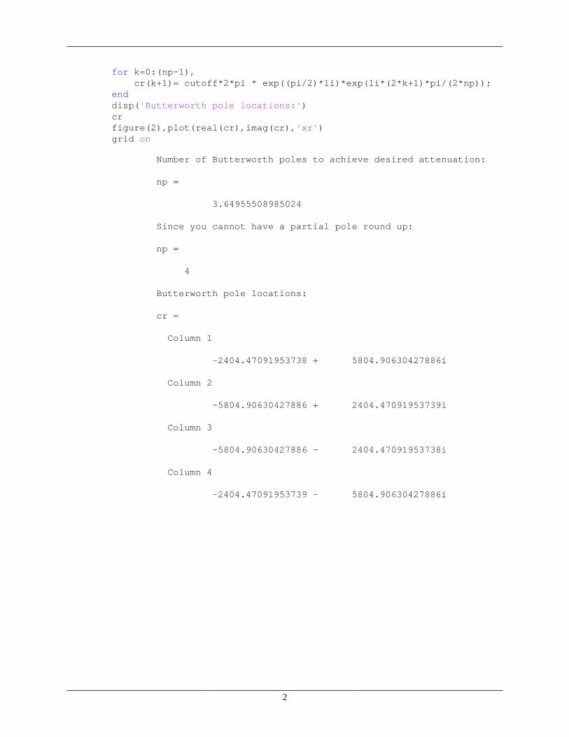
2
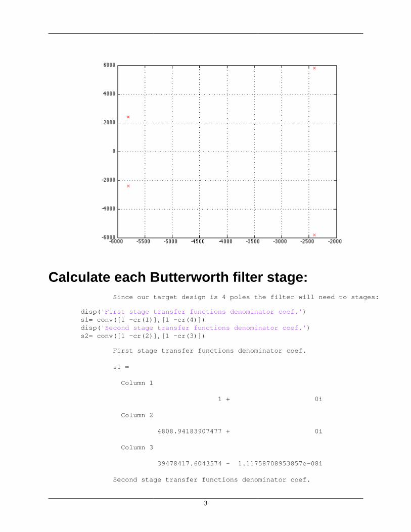
for k=0:(np-1), cr(k+1)= cutoff*2*pi * exp((pi/2)*1i)*exp(1i*(2*k+1)*pi/(2*np));enddisp('Butterworth pole locations:')crfigure(2),plot(real(cr),imag(cr),'xr')grid on
Number of Butterworth poles to achieve desired attenuation:
np =
3.64955508985024
Since you cannot have a partial pole round up:
np =
4
Butterworth pole locations:
cr =
Column 1
-2404.47091953738 + 5804.90630427886i
Column 2
-5804.90630427886 + 2404.47091953739i
Column 3
-5804.90630427886 - 2404.47091953738i
Column 4
-2404.47091953739 - 5804.90630427886i
3
Calculate each Butterworth filter stage:Since our target design is 4 poles the filter will need to stages:
disp('First stage transfer functions denominator coef.')s1= conv([1 -cr(1)],[1 -cr(4)])disp('Second stage transfer functions denominator coef.')s2= conv([1 -cr(2)],[1 -cr(3)])
First stage transfer functions denominator coef.
s1 =
Column 1
1 + 0i
Column 2
4808.94183907477 + 0i
Column 3
39478417.6043574 - 1.11758708953857e-08i
Second stage transfer functions denominator coef.
4
s2 =
Column 1
1 + 0i
Column 2
11609.8126085577 - 1.81898940354586e-12i
Column 3
39478417.6043574 - 1.11758708953857e-08i
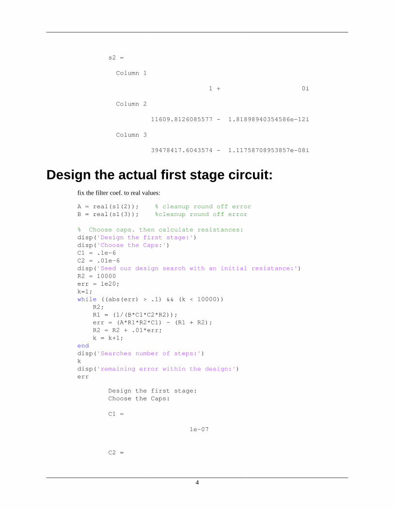
Design the actual first stage circuit:fix the filter coef. to real values:
A = real(s1(2)); % cleanup round off errorB = real(s1(3)); %cleanup round off error
% Choose caps. then calculate resistances:disp('Design the first stage:')disp('Choose the Caps:')C1 = .1e-6C2 = .01e-6disp('Seed our design search with an initial resistance:')R2 = 10000err = 1e20;k=1;while ((abs(err) > .1) && (k < 10000)) R2; R1 = (1/(B*C1*C2*R2)); err = (A*R1*R2*C1) - (R1 + R2); R2 = R2 + .01*err; k = k+1;enddisp('Searches number of steps:')kdisp('remaining error within the design:')err
Design the first stage:Choose the Caps:
C1 =
1e-07
C2 =
5
1e-08
Seed our design search with an initial resistance:
R2 =
10000
Searches number of steps:
k =
1127
remaining error within the design:
err =
-0.0992867286604451
Design the actual second stage circuit:fix the filter coef. to real values:
A = real(s2(2));B = real(s2(3));
% Choose caps. then calculate resistances:disp('Design the second stage:')disp('Choose the Caps:')C3 = .1e-6C4 = .05e-6disp('Seed our design search with an initial resistance:')R4 = 10000;err = 1e20;k=1;while ((abs(err) > .1) && (k < 3000)) R4; R3 = (1/(B*C3*C4*R4)); err = (A*R3*R4*C3) - (R3 + R4); R4 = R4 + .01*err; k = k+1;enddisp('Searches number of steps:')kdisp('remaining error within the design:')err
Design the second stage:Choose the Caps:
C3 =

6
1e-07
C4 =
5e-08
Seed our design search with an initial resistance:Searches number of steps:
k =
1328
remaining error within the design:
err =
-0.0994727122151744
Generate an idealized Bode plot for our des-gined Butterworth filter:
Butterworth transfer function numerators:
n1 = 1 / (R1*R2*C1*C2);n2 = 1 / (R3*R4*C3*C4);% Butterworth transfer function denominators:d1 = [1 ((R1+R2)/(R1*R2*C1)) (1/(R1*R2*C1*C2))];d2 = [1 ((R3+R4)/(R3*R4*C3)) (1/(R3*R4*C3*C4))];
num = n1*n2;den = conv(d1,d2);f1 = tf(num,den);
w = logspace(1,5,1000)*2*pi;[mag,phase,w] = bode(f1,w);grid onmagdb = 20*log10(mag(:));
figure(1),subplot(2,1,1),semilogx(w/(2*pi),magdb),grid onfigure(1),subplot(2,1,2),semilogx(w/(2*pi),phase(:)),grid on
subplot(2,1,1), hold onplot([cutoff cutoff], [max(magdb) min(magdb)], 'g')hold off
subplot(2,1,1), hold onplot([stopband stopband], [max(magdb) min(magdb)], 'r')hold off
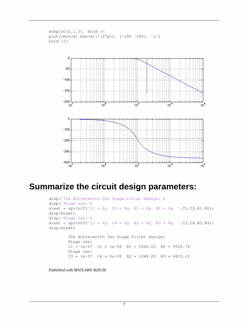
7
subplot(2,1,2), hold onplot([min(w) max(w)]/(2*pi), [-180 -180], 'g')hold off
Summarize the circuit design parameters:disp('The Butterworth Two Stage Filter Design:')disp('Stage one:')stext = sprintf('C1 = %g C2 = %g R1 = %g R2 = %g ',C1,C2,R1,R2);disp(stext)disp('Stage two:')stext = sprintf('C3 = %g C4 = %g R2 = %g R3 = %g ',C3,C4,R3,R4);disp(stext)
The Butterworth Two Stage Filter Design:Stage one:C1 = 1e-07 C2 = 1e-08 R1 = 2660.53 R2 = 9520.76 Stage two:C3 = 1e-07 C4 = 5e-08 R2 = 1048.09 R3 = 4833.61
Published with MATLAB® R2013b

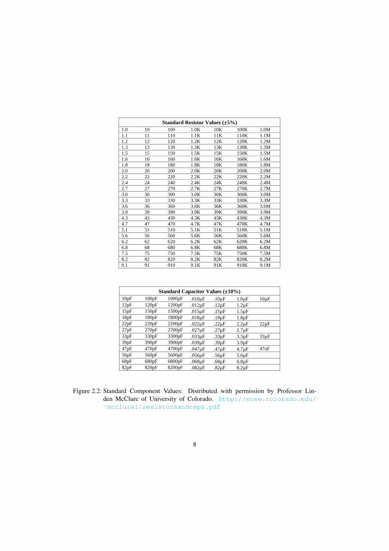
Appendix B: Standard Component ValuesDistributed with permission by Professor Linden McClure of University of Colorado.http://ecee.colorado.edu/˜mcclurel/resistorsandcaps.pdf
6
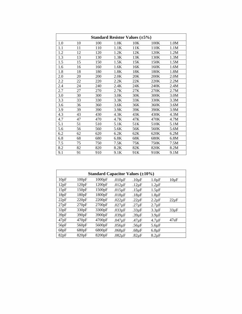
Standard Resistor Values (±±5%)1.0 10 100 1.0K 10K 100K 1.0M1.1 11 110 1.1K 11K 110K 1.1M1.2 12 120 1.2K 12K 120K 1.2M1.3 13 130 1.3K 13K 130K 1.3M1.5 15 150 1.5K 15K 150K 1.5M1.6 16 160 1.6K 16K 160K 1.6M1.8 18 180 1.8K 18K 180K 1.8M2.0 20 200 2.0K 20K 200K 2.0M2.2 22 220 2.2K 22K 220K 2.2M2.4 24 240 2.4K 24K 240K 2.4M2.7 27 270 2.7K 27K 270K 2.7M3.0 30 300 3.0K 30K 300K 3.0M3.3 33 330 3.3K 33K 330K 3.3M3.6 36 360 3.6K 36K 360K 3.6M3.9 39 390 3.9K 39K 390K 3.9M4.3 43 430 4.3K 43K 430K 4.3M4.7 47 470 4.7K 47K 470K 4.7M5.1 51 510 5.1K 51K 510K 5.1M5.6 56 560 5.6K 56K 560K 5.6M6.2 62 620 6.2K 62K 620K 6.2M6.8 68 680 6.8K 68K 680K 6.8M7.5 75 750 7.5K 75K 750K 7.5M8.2 82 820 8.2K 82K 820K 8.2M9.1 91 910 9.1K 91K 910K 9.1M
Standard Capacitor Values (±±10%)10pF 100pF 1000pF .010µF .10µF 1.0µF 10µF12pF 120pF 1200pF .012µF .12µF 1.2µF15pF 150pF 1500pF .015µF .15µF 1.5µF18pF 180pF 1800pF .018µF .18µF 1.8µF22pF 220pF 2200pF .022µF .22µF 2.2µF 22µF27pF 270pF 2700pF .027µF .27µF 2.7µF33pF 330pF 3300pF .033µF .33µF 3.3µF 33µF39pF 390pF 3900pF .039µF .39µF 3.9µF47pF 470pF 4700pF .047µF .47µF 4.7µF 47uF56pF 560pF 5600pF .056µF .56µF 5.6µF68pF 680pF 6800pF .068µF .68µF 6.8µF82pF 820pF 8200pF .082µF .82µF 8.2µF

Appendix C: Anti-aliasing Filter Design Mini-ProjectPROJECT REQUIREMENTS & SPECIFICATIONS DOCUMENT
7
Anti-aliasing Filter Design Mini-Project
PROJECT REQUIREMENTS &SPECIFICATIONS DOCUMENT
Version 1.3.1
Prepared by Prof. Charles R. Tolle
TEAM MEMBERS: EE 464 and CENG 465 Students
PROJECT ADVISOR: Prof. Charles R. Tolle
SPONSOR: SDSM&T ECE Department and its ECE Students
Jan. 12, 2016
Contents
1 Introduction 41.1 Document Purpose . . . . . . . . . . . . . . . . . . . . . . . . . . . . . . . 41.2 Project Description . . . . . . . . . . . . . . . . . . . . . . . . . . . . . . . 41.3 Document Layout . . . . . . . . . . . . . . . . . . . . . . . . . . . . . . . . 5
2 Project Requirements and Specifications 62.1 Requirements . . . . . . . . . . . . . . . . . . . . . . . . . . . . . . . . . . 62.2 Specifications . . . . . . . . . . . . . . . . . . . . . . . . . . . . . . . . . . 6
Bibliography 11
2
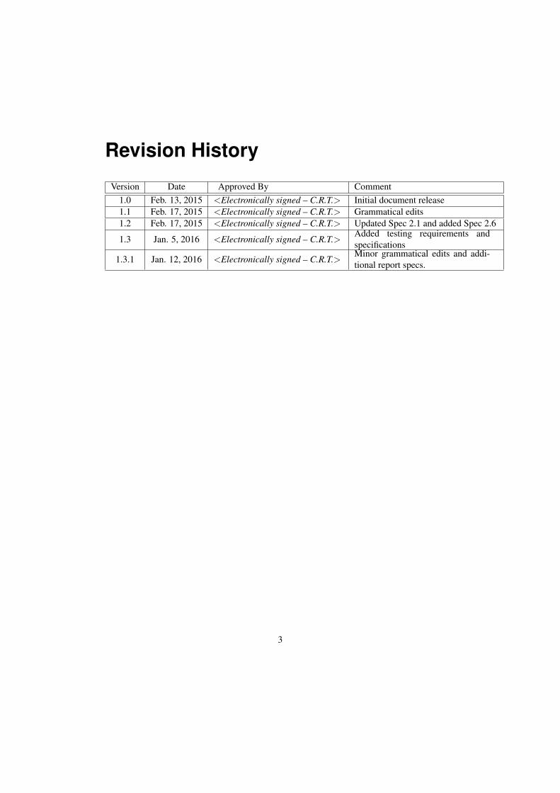
Revision History
Version Date Approved By Comment1.0 Feb. 13, 2015 <Electronically signed – C.R.T.> Initial document release1.1 Feb. 17, 2015 <Electronically signed – C.R.T.> Grammatical edits1.2 Feb. 17, 2015 <Electronically signed – C.R.T.> Updated Spec 2.1 and added Spec 2.6
1.3 Jan. 5, 2016 <Electronically signed – C.R.T.>Added testing requirements andspecifications
1.3.1 Jan. 12, 2016 <Electronically signed – C.R.T.>Minor grammatical edits and addi-tional report specs.
3
1 Introduction
1.1 Document PurposeThe purpose of this document is to provide an example requirements and specification docu-ment for South Dakota School of Mines and Technology’s (SDSM&T’s) Senior Design ClassEE 464 and CENG 464. Traditionally requirements and specification have been separated intwo different documents; however due to the size and scope of most senior projects, we willcombine these documents into a single document. Moreover, system requirements capture aproject’s system level needs/goals for a project, while project specifications are meant to di-rect/constrain the designer on how those goals are achieve. In our class, requirements will bethought of as the needs, functions, goals, and features of a project, while specifications will betreated as design guidelines, constraints, limitations, ranges, technological choices, etc. Therequirements are what needs to be accomplished or included, while specs are ranges, values,technological choices used in achieving the goal.
Within large traditional engineering projects, requirement and specification traceability isvery important. Many industries such as health care, transportation, communications, aviation,military, etc. require extensive accountability within their design processes. Such detailed ac-countability for such industries is required due to both financial as well as a legal and technicalissues. Generally, main line engineering teams are not allowed to work on items that do notstem directly from a project requirement or specification, thus the development of these doc-uments is very important. Moreover, these documents act as a contract with the customer forwhat will be delivered at the end of the project, i. e. if there isn’t a requirement for an item itisn’t included or worked on during the project.
Each project needs to develop its own requirements and specifications document. Thesedocuments constitute a significant effort within each Senior Design I project. Moreover, thisdocument acts as the guiding force behind the design and deliverables of the project. It guidesthe majority of the work preformed between the Preliminary Design Review (PDR) and theCritical Design Review (CDR), and defines the key deliverable items to the customer at theend of the project.
1.2 Project DescriptionThe EE-464/CENG-464 mini-project goals are to provide ECE students with a small examplePCB-based design project that elucidates project requirements and specifications as well asensures that all ECE students have designed a PCB board within a modern electrical ComputerAided Design (CAD) package before graduation from the SDSM&T’s ECE department. Theproject requirements are given below in Section 2.1. You will be required to design an anti-aliasing filter and its circuit, analyze the design within SPICE to ensure that your design meets
4
the project’s design specs (see Section 2.2) and lay out a small circuit board to implement thedesign. Once these steps are complete, you are to write a short report detailing your designprocess, calculations, simulations, and lay outs. The projects requirements and spec’s aredocumented below.
1.3 Document LayoutThe sections that follow provide a simplified project example based on our mini-project. Eachrequirement will be identified through the paragraph numbering structure of this document.The document structure shall be as follows:
1.w.x.y.z
Example tree structure is given below:
1 level 1 item
1.1 level 2 item
1.2 level 2 item
2 level 1 item
Requirements shall be contained in Section 2.1 of this document. The corresponding Spec-ifications are contained in section 2.2 of this document. The “1.w.x.y.z” numbering schemeshall identify the requirement and specification hierarchy.
5
2 Project Requirements andSpecifications
2.1 Requirements1 Anti-alaising Filter
Design an anti-aliasing filter that minimizes the distortion in the pass band
2 Circuit DesignDesign a circuit using real components that implements the filter design
3 PC Board DesignLayout a pc-board that implements the filter design
4 Prototype testing, verification, and validationPerform experimental and quality control checks on the prototype hardware to ensureall requirements and specifications within this document have been met.
5 ReportWrite a short but detailed report on the design and the process you used within this miniproject – be precise & concise
2.2 Specifications1 Anti-alaising Filter
1.1 Design a Butterworth filter
1.2 Cutoff frequency of 5kHz
1.3 Starting stop-band frequency of 10kHz
1.4 Allow at most -6dB pass-band attenuation
1.5 Maintain at least -23dB stop-band attenuation
2 Circuit Design
2.1 Utilize a Sallen-Key circuit topology, see Fig. 2.1. In this topology, the circuits’parameters, R1, R2, C1, C2, are defined by the designer to achieve the designgoals.
6
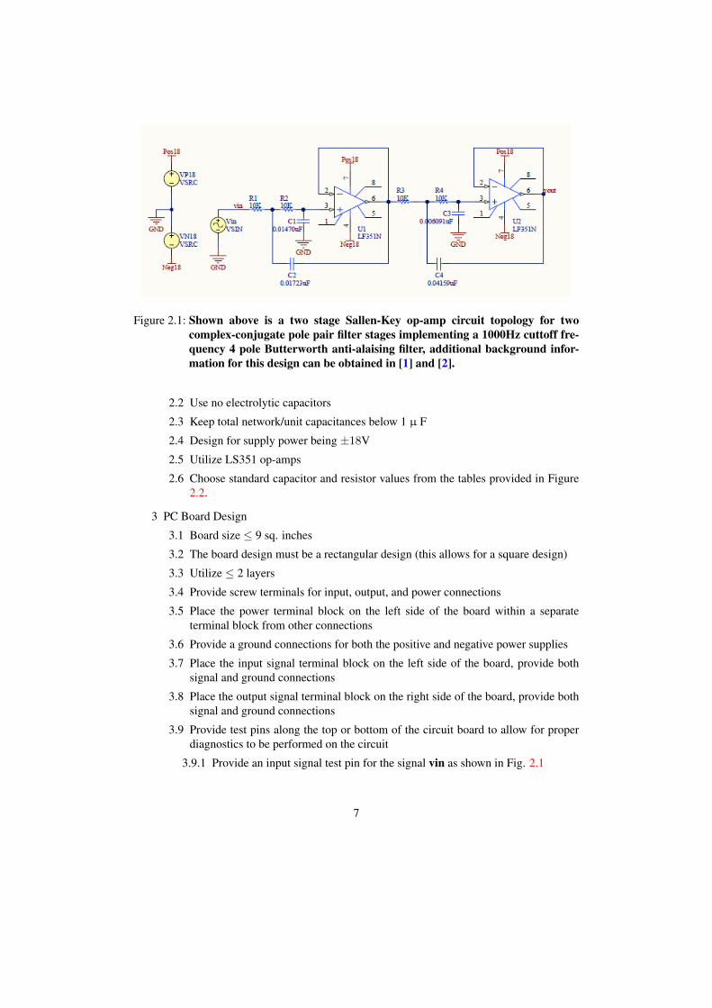
Figure 2.1: Shown above is a two stage Sallen-Key op-amp circuit topology for twocomplex-conjugate pole pair filter stages implementing a 1000Hz cuttoff fre-quency 4 pole Butterworth anti-alaising filter, additional background infor-mation for this design can be obtained in [1] and [2].
2.2 Use no electrolytic capacitors
2.3 Keep total network/unit capacitances below 1 µ F
2.4 Design for supply power being ±18V
2.5 Utilize LS351 op-amps
2.6 Choose standard capacitor and resistor values from the tables provided in Figure2.2.
3 PC Board Design
3.1 Board size ≤ 9 sq. inches
3.2 The board design must be a rectangular design (this allows for a square design)
3.3 Utilize ≤ 2 layers
3.4 Provide screw terminals for input, output, and power connections
3.5 Place the power terminal block on the left side of the board within a separateterminal block from other connections
3.6 Provide a ground connections for both the positive and negative power supplies
3.7 Place the input signal terminal block on the left side of the board, provide bothsignal and ground connections
3.8 Place the output signal terminal block on the right side of the board, provide bothsignal and ground connections
3.9 Provide test pins along the top or bottom of the circuit board to allow for properdiagnostics to be performed on the circuit
3.9.1 Provide an input signal test pin for the signal vin as shown in Fig. 2.1
7
Standard Resistor Values (±±5%)1.0 10 100 1.0K 10K 100K 1.0M1.1 11 110 1.1K 11K 110K 1.1M1.2 12 120 1.2K 12K 120K 1.2M1.3 13 130 1.3K 13K 130K 1.3M1.5 15 150 1.5K 15K 150K 1.5M1.6 16 160 1.6K 16K 160K 1.6M1.8 18 180 1.8K 18K 180K 1.8M2.0 20 200 2.0K 20K 200K 2.0M2.2 22 220 2.2K 22K 220K 2.2M2.4 24 240 2.4K 24K 240K 2.4M2.7 27 270 2.7K 27K 270K 2.7M3.0 30 300 3.0K 30K 300K 3.0M3.3 33 330 3.3K 33K 330K 3.3M3.6 36 360 3.6K 36K 360K 3.6M3.9 39 390 3.9K 39K 390K 3.9M4.3 43 430 4.3K 43K 430K 4.3M4.7 47 470 4.7K 47K 470K 4.7M5.1 51 510 5.1K 51K 510K 5.1M5.6 56 560 5.6K 56K 560K 5.6M6.2 62 620 6.2K 62K 620K 6.2M6.8 68 680 6.8K 68K 680K 6.8M7.5 75 750 7.5K 75K 750K 7.5M8.2 82 820 8.2K 82K 820K 8.2M9.1 91 910 9.1K 91K 910K 9.1M
Standard Capacitor Values (±±10%)10pF 100pF 1000pF .010µF .10µF 1.0µF 10µF12pF 120pF 1200pF .012µF .12µF 1.2µF15pF 150pF 1500pF .015µF .15µF 1.5µF18pF 180pF 1800pF .018µF .18µF 1.8µF22pF 220pF 2200pF .022µF .22µF 2.2µF 22µF27pF 270pF 2700pF .027µF .27µF 2.7µF33pF 330pF 3300pF .033µF .33µF 3.3µF 33µF39pF 390pF 3900pF .039µF .39µF 3.9µF47pF 470pF 4700pF .047µF .47µF 4.7µF 47uF56pF 560pF 5600pF .056µF .56µF 5.6µF68pF 680pF 6800pF .068µF .68µF 6.8µF82pF 820pF 8200pF .082µF .82µF 8.2µF
Figure 2.2: Standard Component Values: Distributed with permission by Professor Lin-den McClure of University of Colorado. http://ecee.colorado.edu/
˜mcclurel/resistorsandcaps.pdf
8

3.9.2 Provide an output test pin for the first stage of the filter, i.e connected to pin 6of U1 LF351N shown in Fig. 2.1
3.9.3 Provide an output signal test pin for the signal vout as shown in Fig. 2.1
3.9.4 Provide adequate space to allow for easy connection of scope probes to eachtest pin
3.9.5 Co-locate these test pins in a line at the edge of the board
3.10 Provide mounting holes in the corners of the board
3.11 Each mounting hole must allow for the usage of a 14 -20 bolt
4 Prototype testing, verification, and validation
4.1 Develop a power up test
4.1.1 Apply ±18 Volts and ground power
4.1.2 Apply grounded inputs
4.1.3 Check for circuit shorts
4.1.4 Check for stable ground output
4.2 Develop a 1kHz sine wave of 1 Volt amplitude test
4.2.1 Apply ±18 Volt power and ground
4.2.2 Using a standard function generator apply a 1kHz sine wave of 1 Volt ampli-tude to the input terminal block, i.e. vin as shown in Fig. 2.1
4.2.3 Measure the circuits output at the output terminal block, i.e. vout as shownin Fig. 2.1
4.2.4 Compare results with simulations preformed under Spec. 5.6
4.2.5 Insure measured results are within ±10% from the simulations to count aspassage
4.2.6 Insure the pass band requirement under Spec. 1.4 has been met
4.3 Develop a 10kHz sine wave of 1 Volt amplitude test
4.3.1 Apply ±18 Volt power and ground
4.3.2 Using a standard function generator apply a 10kHz sine wave of 1 Volt am-plitude to the input terminal block, i.e. vin as shown in Fig. 2.1
4.3.3 Measure the circuits output at the output terminal block, i.e. vout as shownin Fig. 2.1
4.3.4 Compare results with simulations preformed under Spec. 5.7
4.3.5 Insure measured results are within ±10% from the simulations to count aspassage
4.3.6 Insure the stop band requirement under Spec. 1.5 has been met
4.4 Develop a series of pass band checks ranging from 100Hz to 10kHz in steps of 2utilizing sine waves of 1 Volt amplitude test
9

4.4.1 Apply ±18 Volt power and ground
4.4.2 Using a standard function generator apply a the test signal sine wave of 1 Voltamplitude to the input terminal block, i.e. vin as shown in Fig. 2.1
4.4.3 Measure the circuits output at the output terminal block, i.e. vout as shownin Fig. 2.1
4.4.4 Insure the pass or stop band requirements have been met under Specs. 1.4 and1.5
5 Report
5.1 Include design description and purpose
5.2 Include all design calculations
5.3 Include any solution codes
5.4 Include designed frequency domain response plots, i.e. ideally designed Bode plot
5.5 Include circuit drawings, with clearly labeled component values, chip numbers,etc.
5.6 Include SPICE transient circuit simulations for a 1kHz sine wave of 1 Volt ampli-tude
5.7 Include SPICE transient circuit simulations for a 10kHz sine wave of 1 Volt am-plitude
5.8 Include SPICE AC analysis circuit simulations plots, i.e. realized bode plot
5.9 Include your final pc board layout, show dimensional markings
5.10 Include a bill of materials list
5.11 Include all appropriate citations and bibliography as needed
5.12 Include labels and figure captions that fully communicate what information is con-veyed in each figure
5.13 If Matlab Code is used to design the filter components the following additionalspecification are required
5.13.1 Insure all Matlab figures and outputs are appropriately labeled
5.13.2 Clearly communicate how, why and what information each figure provides
5.13.3 Provide a copy of the code within an Appendix
5.13.4 Clearly document what and how the code works
5.13.5 Provide a clear final solution output of the code and a description of how itsresults are used within the final design
5.14 While the report must include the above items 5.1-5.13, a complete report furtherrequires an actual description of the work performed and a full description of theanalysis also preformed.
10

Bibliography
[1] Gordon J. Deboo. An RC Active Filter Design Handbook. National Aeronautics and SpaceAdministration, 1977.
[2] Numerous-Anonymous. Sallen-key topology. Webpage from Wikipedia, the free ency-clopedia. http://en.wikipedia.org/wiki/Sallen-Key topology.
11