Embed Size (px)
Citation preview
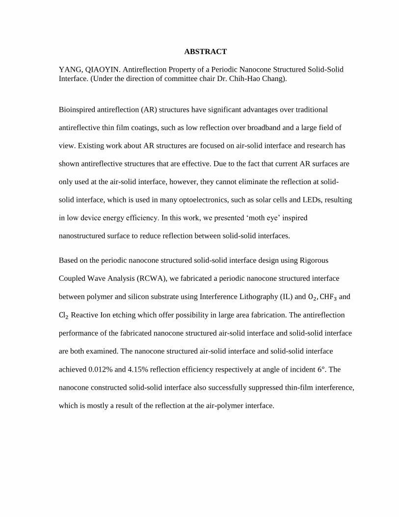
ABSTRACT
YANG, QIAOYIN. Antireflection Property of a Periodic Nanocone Structured Solid-Solid
Interface. (Under the direction of committee chair Dr. Chih-Hao Chang).
Bioinspired antireflection (AR) structures have significant advantages over traditional
antireflective thin film coatings, such as low reflection over broadband and a large field of
view. Existing work about AR structures are focused on air-solid interface and research has
shown antireflective structures that are effective. Due to the fact that current AR surfaces are
only used at the air-solid interface, however, they cannot eliminate the reflection at solid-
solid interface, which is used in many optoelectronics, such as solar cells and LEDs, resulting
in low device energy efficiency. In this work, we presented ‘moth eye’ inspired
nanostructured surface to reduce reflection between solid-solid interfaces.
Based on the periodic nanocone structured solid-solid interface design using Rigorous
Coupled Wave Analysis (RCWA), we fabricated a periodic nanocone structured interface
between polymer and silicon substrate using Interference Lithography (IL) and and
Reactive Ion etching which offer possibility in large area fabrication. The antireflection
performance of the fabricated nanocone structured air-solid interface and solid-solid interface
are both examined. The nanocone structured air-solid interface and solid-solid interface
achieved 0.012% and 4.15% reflection efficiency respectively at angle of incident . The
nanocone constructed solid-solid interface also successfully suppressed thin-film interference,
which is mostly a result of the reflection at the air-polymer interface.

We have also developed a contrast model to predict nanocone structured solid-solid interface
antireflection performance based on the interference pattern of the reflection efficiency over
broadband. This work presented a scheme to eliminate solid-solid interface reflection and the
idea can be further implemented into different solid-solid interfaces, such as organic solar
cells.

© Copyright 2012 by Qiaoyin Yang
All Rights Reserved
Antireflection Property of a Periodic Nanocone Structured Solid-Solid Interface
by
Qiaoyin Yang
A thesis submitted to the Graduate Faculty of
North Carolina State University
in partial fulfillment of the
requirements for the Degree of
Master of Science
Aerospace Engineering
Raleigh, North Carolina
2012
APPROVED BY:
_______________________________ ______________________________
Dr. Xiaoning Jiang Dr. Yong Zhu
________________________________
Dr. Chih-Hao Chang
Chair of Advisory Committee

ii
DEDICATION
To Mom, Jianying Liang, Dad, Zhuangtian Yang, my brothers and sisters,
Huiwen, Jiheng, Yanfeng, Chunren Yang.
iii
BIOGRAPHY
Qiaoyin Yang is from Maoming, Guangdong Province. It is located in the south of China, a
very beautiful coastal city. It’s famous for its fresh fruits and seafood. It is the home for Lichi.
Guangdong Province has the best food in China and Maoming has the best food in
Guangdong.
Qiaoyin has her Bachelor of Science in Electromechanical Engineering from Guangdong
University of Technology in 2010. She likes adventures and after graduated, she decided to
go abroad for graduate school. She obtained her Master of Science in Aerospace Engineering
from North Carolina State University and had enjoyed the time in North Carolina.
When she has free time, she likes to spend time with her family and friends.

iv
ACKNOWLEDGMENTS
I want to thank my advisor, Dr. Chih-Hao Chang, for all the support and advice in research.
Chi is an extraordinary advisor. His enthusiasm and ideas about research have always been
very inspiring. His knowledge and experience have helped me overcome a lot of obstacles in
research.
I want to thank my labmates Xu Zhang and Abhijeet Bagal. I had great talks with them and
thank them for their support in the research. Special thanks to Wei Guo, for his support in
setting up a broadband measurement system. Thanks for all the technical support I get from
NCSU Nanofabricaton Center and Analytical Instrumentation Facility.
Special thanks to all my friends from North Carolina. Judy Brown, Whitney Lohmeyer,
Melody Lohmeyer and Bill Lohmeyer. They have been supporting me since I started my
graduate school in NCSU. Their support has been tremendous and they have made my life
much more colorful and joyful. I also want to thank my previous labmates, Andy Richards
and Shaphan Jernigan.
I want to thank my parents, my brothers and sisters for their unconditional love and support.
Mom has been the greatest support. Dad’s emphasis in education has made me where I am.
My elder brother and elder sisters, their support and love is unconditional. Younger brother
has been the sweetest brother ever.
v
TABLE OF CONTENTS
LIST OF TABLES ........................................................................................................................... vi
LIST OF FIGURES ........................................................................................................................ vii
Chapter 1 Introduction .................................................................................................................... 1
1.1 Reflection Mechanism ............................................................................................................ 4
1.2 Periodic Nanocone Structured Solid-Solid Interface .............................................................. 6
1.3 Light Interference Theory ....................................................................................................... 7
1.4 Thesis Structure ...................................................................................................................... 9
Chapter 2 Design of Periodic Nanocone Structured Solid-Solid Interface ............................... 10
2.1 Rigorous Coupled Wave Analysis Theory ........................................................................... 10
2.2 Polymer-Nanocone-Silicon Interface Design ....................................................................... 12
Chapter 3 Fabrication of Periodic Nanocone Structured Solid-Solid Interface ....................... 18
3.1 Laser Interference Lithography ............................................................................................ 18
3.2 Interference Lithography Stack Design ................................................................................ 20
3.3 Duty Cycle Control............................................................................................................... 21
3.4 Polymer-Nanocone-Si Interface Fabrication Process ........................................................... 25
Chapter 4 Polymer-Nanocone-Si Interface Antireflection Characterization ........................... 32
4.1 RCWA based Polymer-nanocone-Si Interface Modeling..................................................... 32
4.2 Broadband and Wide Angle Reflection Efficiency Measurement ....................................... 35
4.3 Reflection Efficiency Contrast Model .................................................................................. 42
Chapter 5 Conclusion ..................................................................................................................... 50
REFERENCES ............................................................................................................................... 52
APPENDICES ................................................................................................................................ 55
Appendix A ..................................................................................................................................... 56
vi
LIST OF TABLES
Table 2-1: Parameters of the RCWA numerical Model, polymer(730nm)-nanocone-Si stack ............ 13
Table 2-2: The stack design for the PNC interface with paraboloidal-shaped nanocone ..................... 14
Table 3-1: The optimization of antireflection coating thickness parameter set-up .................. 21
Table 3-2: Reactive ion etching parameters for 2D-200nm period pattern transfer process ................ 29
Table 4-1: Parameter set-up for RCWA numerical Model based on the fabricated PNCSI,
Polymer(730nm)-nanocone-Si stack .................................................................................................... 33
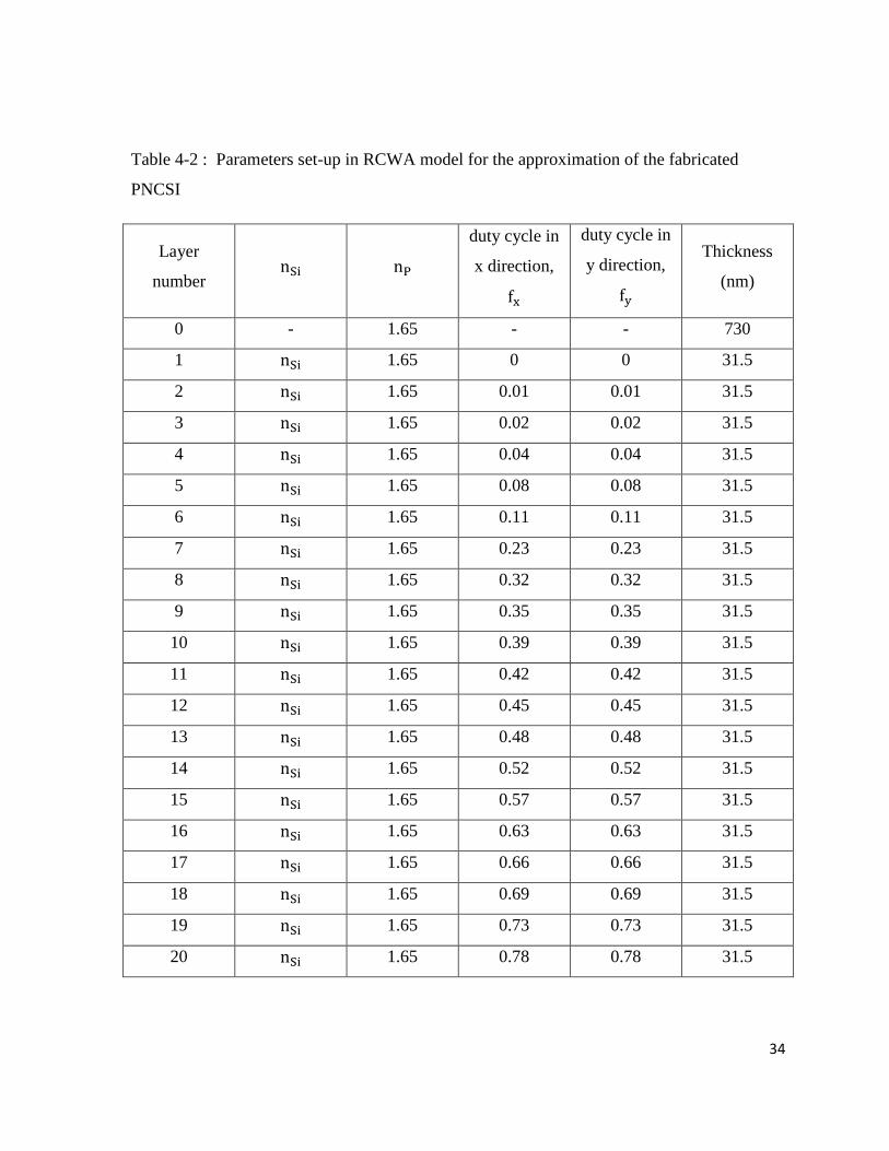
Table 4-2 : Parameters set-up in RCWA model for the approximation of the fabricated PNCSI ....... 34
Table 4-3: Contrast and the corresponding approximated reflection at polymer-nanocone interface .. 48
vii
LIST OF FIGURES
Figure 1-1: (a) Moth eye surfaces in detail, showing the local arrangement of domains with highly
ordered nipple arrays. The scale bar is [3] (b) Scanning-electron micrograph (SEM) of
fabricated nanostructured gradient reflective index grating [6]. (c) SEM of subwavelength
nanostructured surface [7] (d) SEM of silicon nanotips on a 6-inch silicon wafer [8] (e) SEM of 2
dimensional grating with conical profile on silicon substrate [9] (f) SEM of high-density, high aspect
ratio corkscrew-like silicon nanotips [10]. ............................................................................................. 3
Figure 1-2: A schematic diagram of typical superstrate type thin film solar cell structure and
designed cell structure with antireflective layers (sample B) [5]. .......................................................... 3
Figure 1-3: An incoming wave whose field is perpendicular to the plane of incident. ...................... 4
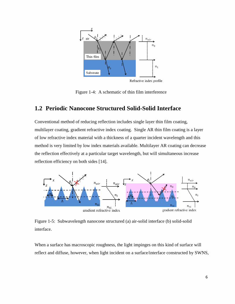
Figure 1-4: A schematic of thin film interference ................................................................................. 6
Figure 1-5: Subwavelength nanocone structured (a) air-solid interface (b) solid-solid interface. ........ 6
Figure 2-1: A schematic for a stack of homogeneous and periodic layers .......................................... 11
Figure 2-2: A schematic diagram of (a) a paraboloidal-shape nanocone approximated by 10 layers of
periodic layers, thickness of polymer layer , nanocone height , period and , referactive
index of polymer, silicon are respectively (b) reflection at a semi-infinite air and semi-
infinite polymer stack. .......................................................................................................................... 13
Figure 2-3: (color online) The RCWA calculated wide angle reflection efficiency of the polymer-
nanocone-Si interface design, TE mode. A reflection efficiency comparison between polymer- bare
silicon interface (blue line) and air-polymer interface (black line) is provided. .................................. 15
Figure 2-4: (color online) The RCWA calculated wide angle reflection efficiency of the polymer-
nanocone-Si interface design, TM mode. A reflection efficiency comparison between polymer- bare
silicon interface (blue line) and air-polymer interface (black line) is provided. .................................. 16
Figure 2-5: (color online) Simulated broadband reflection efficiency for the designed PNCSI. A
reflection efficiency comparison between polymer-silicon interface (blue line) and air-polymer
interface (black line) is provided. ......................................................................................................... 16
Figure 3-1: a schematic diagram of interference lithography .............................................................. 19
Figure 3-2: A schematic of the Lloyd’s mirror interferometer set-up [19]. ........................................ 19
Figure 3-3: (a) A schematic of reflected beam from interface 2 will degrade photoresist pattern (b) A
schematic of stack design for fabricating PNC. is used as a hard mask. ..................................... 20
Figure 3-4: Simulated reflection as a function of ARC thickness at photoresist-ACR interface. ....... 21
viii
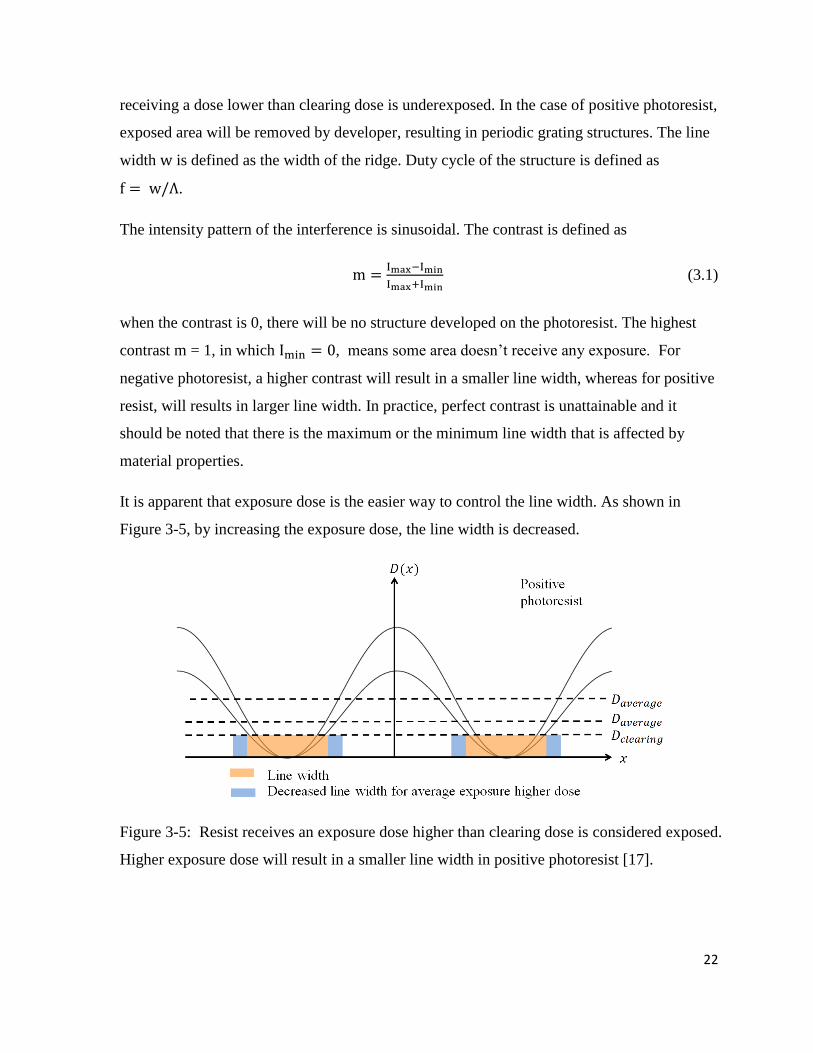
Figure 3-5: Resist receives an exposure dose higher than clearing dose is considered exposed. Higher
exposure dose will result in a smaller line width in positive photoresist [17]. ..................................... 22
Figure 3-6: Line width as a function of exposure dose for (a) 1 Dimensional (1D) photoresist grating,
photoresist thickness 200nm, periodicity 200nm, (b) 1D photoresist grating, photoresist thickness
500nm, periodicity 500nm, (c) 2 Dimensional (2D) photoresist grating, photoresist thickness 200nm,
periodicity 200nm, (d) 2D photoresist grating, photoresist thickness 500nm, periodicity 500nm. The
inset micrographs are the corresponding patterns. ............................................................................... 24
Figure 3-7: The PNCSI fabrication process starts with (a) spin-coat, HSQ, ARC, photoresist (b)
photoresist is exposed and developed, (c) RIE transfer the photoresist pattern into ARC layer, (d)
RIE transfer the pattern into , (e) Etch Silicon with RIE, (f) photoresist is spin- coated
on top of the nanocone structures. This process creates the polymer-nanocone-silicon interface. ...... 26
Figure 3-8: Photoresist is exposed and developed. (A) A titled view of the edge of the pattern, (b)
top view of the photoresist pattern, (c) a zoomed-in image of the 2D grating pattern. The scale bar is
shown in each figure. ............................................................................................................................ 27
Figure 3-9 : 2D-200nm periodicity pattern after 1.8min RIE (A) A titled view of the edge of
the sample, (b) top view after RIE, (c) a zoomed-in image of the top surface. .............................. 27
Figure 3-10: 2D-200nm periodicity pattern after 1.8min RIE and 10.5min RIE (A) a
tilted view of the edge after RIE , (b) top view after RIE, (c) a zoomed-in image of the top
surface. ................................................................................................................................................. 28
Figure 3-11: A tilted view of the surface of the 2D-200nm pattern after 1.8min RIE and
10.5min RIE and (a) 5min RIE (b) 8min RIE (c) 12min RIE. ............................... 28
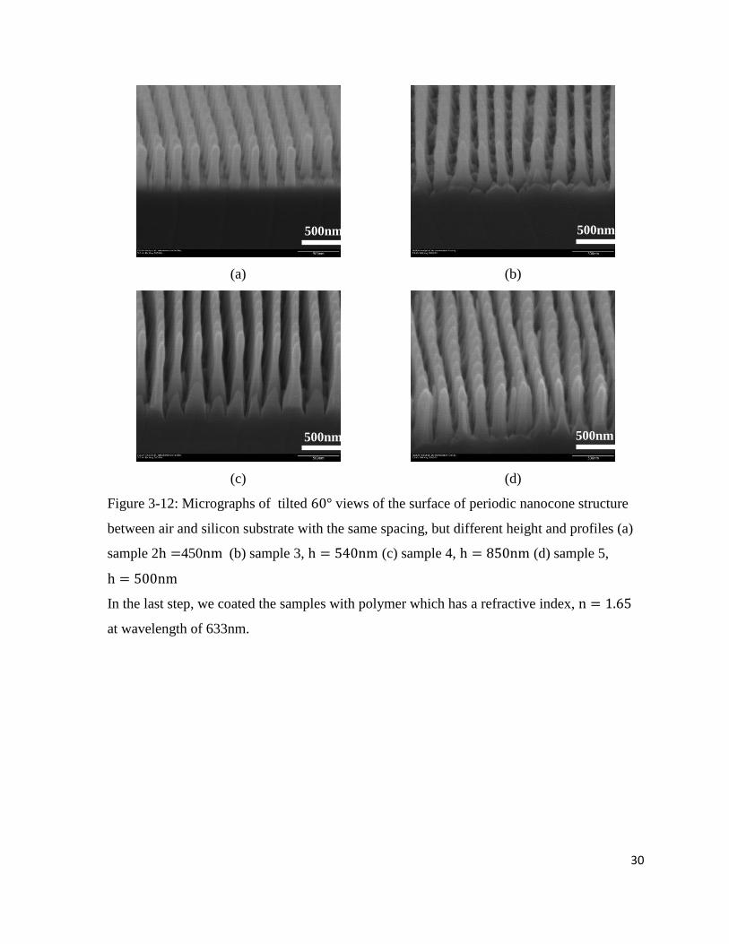
Figure 3-12: Micrographs of tilted views of the surface of periodic nanocone structure between
air and silicon substrate with the same spacing, but different height and profiles (a) sample
2 450 (b) sample 3, (c) sample 4, (d) sample 5, .......... 30
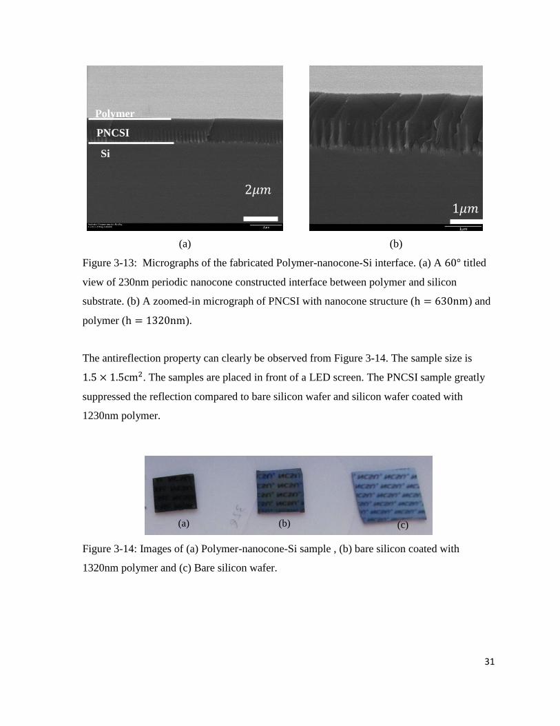
Figure 3-13: Micrographs of the fabricated Polymer-nanocone-Si interface. (a) A titled view of
230nm periodic nanocone constructed interface between polymer and silicon substrate. (b) A
zoomed-in micrograph of PNCSI with nanocone structure ( ) and polymer ( ).
.............................................................................................................................................................. 31
Figure 3-14: Images of (a) Polymer-nanocone-Si sample , (b) bare silicon coated with 1320nm
polymer and (c) Bare silicon wafer. ..................................................................................................... 31
Figure 4-1: Geometry of the homogenous and periodic layers with gradient refractive index ........... 33
ix
Figure 4-2: (a) Wide angle reflection efficiency measurement set-up (b) broadband reflection
efficiency measurement set-up. ............................................................................................................ 35
Figure 4-3: (Color online) Measured reflected efficiencies of the zero order of the air-nanocone-
silicon interface at wavelength , (a)TE mode, (b) TM mode. The solid lines are the
corresponding simulated efficiencies using RCWA. ............................................................................ 37
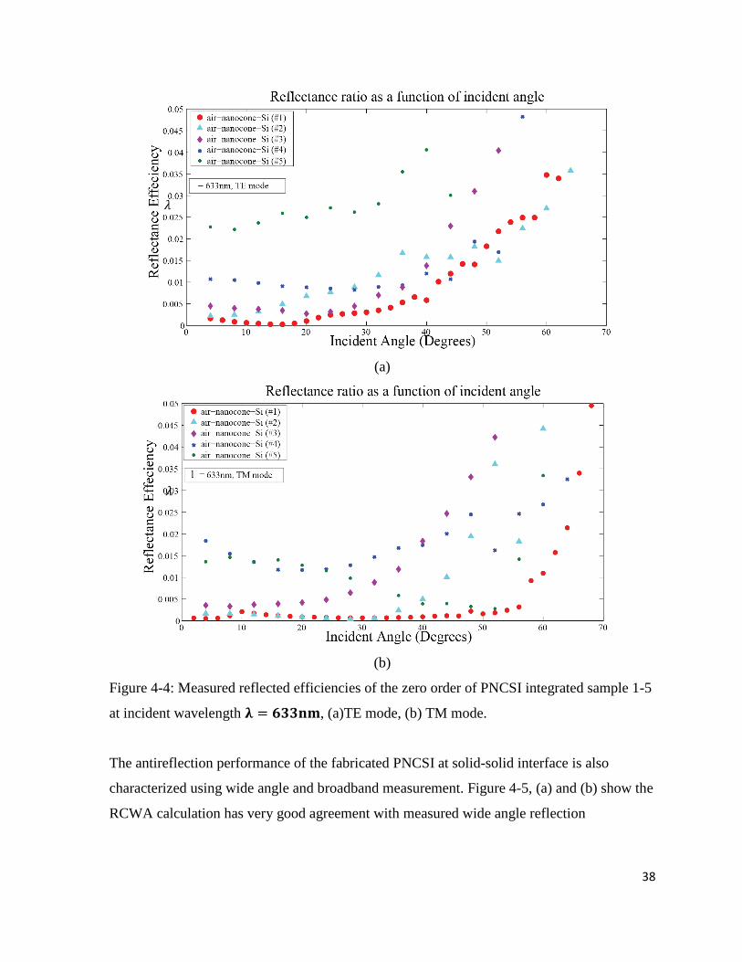
Figure 4-4: Measured reflected efficiencies of the zero order of PNCSI integrated sample 1-5 at
incident wavelength , (a)TE mode, (b) TM mode. .......................................................... 38
Figure 4-5: (Color online) Measured reflected efficiencies of the zero order of the nanocone
structured surface, silicon coated with 1320nm polymer and silicon coated with 730nm polymer
under incident wavelength , (a) TE mode, (b) TM mode. The solid lines are the
corresponding simulated efficiencies using RCWA. ............................................................................ 40
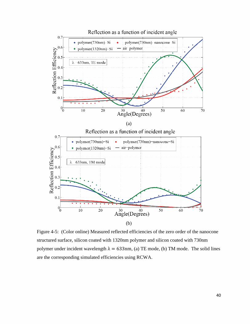
Figure 4-6: (Color online) Measured reflected efficiencies of the polymer-nanocone-Si interface,
730nm polymer-Si interface, 1320nm-Polymer-Si interface, at an incident angle The solid lines
are measured data and the dotted line are the corresponding simulated efficiencies using RCWA. .... 41
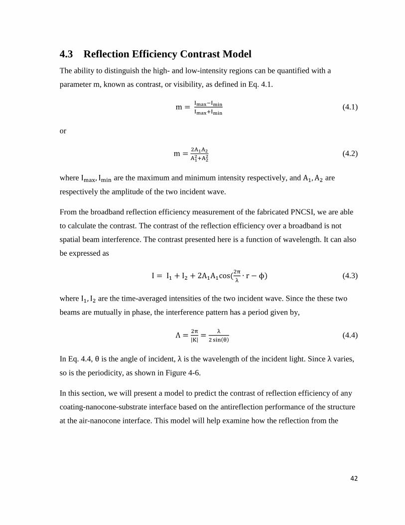
Figure 4-7: A schematic of (a) reflection at air-nanocone interface is suppressed, (b) beam
interference in polymer-nanocone-substrate stack. The reflection from polymer-nanocone interface
interfere with reflection from air-polymer interface . ............................................................... 43
Figure 4-8: (Color online) Measured and simulated reflected efficiencies for the fabricated the
polymer-nanocone-Si stack at an incident angle 7.5°, (a) sample 2, (b) sample 3, (c) sample 4, (d)
sample 5. The solid lines are measured data and the dotted line are the corresponding simulated
efficiencies using RCWA. .................................................................................................................... 45
Figure 4-9: Contrast as a function of Reflection Efficiency , Each red dot corresponds to a
sample. .................................................................................................................................................. 48
1
Chapter 1 Introduction
Conventional single layer or multiple layer thin-film antireflection coatings have been widely
used to reduce the Fresnel reflection. Other methods include gradient refractive index coating
[1], and nanoporous films[2]. However there are intrinsic defects associated with these
methods such as material selection, adhesion, thermal mismatch, material stability, and
diffusion of one material into another material. Meanwhile, there are a variety of AR
structures existing in nature, such as on the corneas of moth and butterfly eyes [3].
Researchers and engineers have been inspired by these structures in nature and emulated
these structures. “Moth eye”, depicted in Figure 1-1(a), consists of nanostructures arranged in
a hexagonal array with periodicity of around 240nm [3]. Researchers have demonstrated
different efforts in this field, such as fabrication [6-10], antireflection simulation [6, 22, 23],
applications of such bio-inspired surfaces[5, 21], etc. The moth eye structure was first
reproduced at its correct scale by crossing three gratings at using lithographic
techniques [4].
The “moth eye” structure is particularly useful because it can achieve broadband and wide
angle antireflection. This type of structure is a very fine surface structure with a pattern
smaller than the wavelength of light and is often referred to as subwavelength nanostructures
(SWNS).
The SWS are generally structured with a high aspect ratio and suppresses reflection
drastically over a wide spectral bandwidth and a large field of view. The two dimensional
SWNS is designed to be independent of the polarization direction. The SWNS constructed
interface can ideally be a gradient refractive index interface. However, this antireflection
nanostructure is at the air and solid interface which is very fragile and the application is
limited.
When light impinges on a multiple layers of material with different thickness, within each
layer of material, the multiple reflection and transmission beams will interfere with each
2
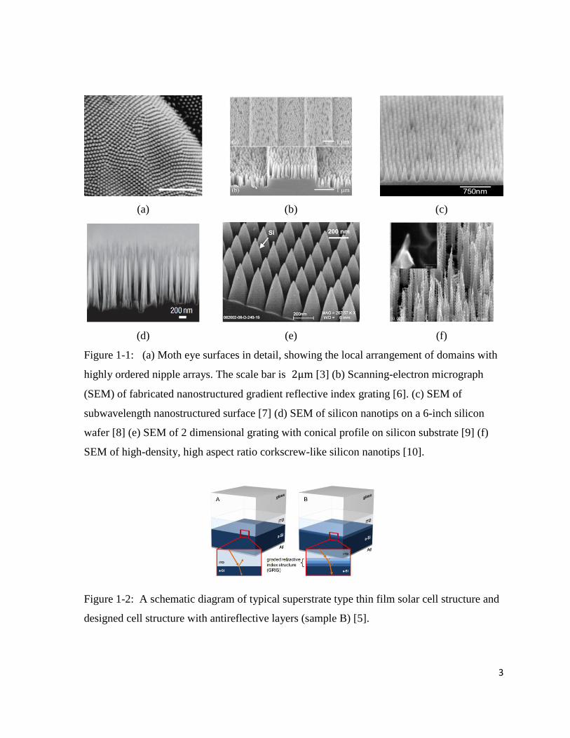
other. The iridescent colors of a thin film of oil on water or soap bubble are good examples.
For solar cells, the optical loses between different layers (substrate, photovoltaic layer, buffer
layers) caused a considerable amount of optical lose due to this effect, see Figure 1-2[5]. In
most cases, traditional antireflection coating can’t be implemented inbetween these layers to
eliminate reflection because limited materials available, effects on the functionality of
devices, etc. Meanwhile, the SWS, especially cone shaped nanostructures has great potential
when integrated with layer based devices, such as solar cells and light-emitting diodes (LEDs)
to reduce reflection and increase transmission.
This thesis will present our approach in eliminating thin film interference by constructing a
periodic nanocone structure at the interface of solid materials. Various methods of fabricating
SWS have been demonstrated and reflection is suppressed.
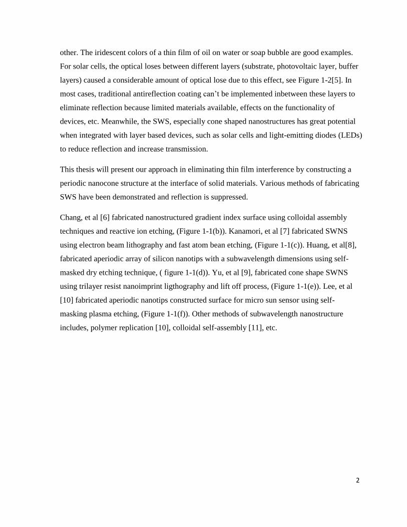
Chang, et al [6] fabricated nanostructured gradient index surface using colloidal assembly
techniques and reactive ion etching, (Figure 1-1(b)). Kanamori, et al [7] fabricated SWNS
using electron beam lithography and fast atom bean etching, (Figure 1-1(c)). Huang, et al[8],
fabricated aperiodic array of silicon nanotips with a subwavelength dimensions using self-
masked dry etching technique, ( figure 1-1(d)). Yu, et al [9], fabricated cone shape SWNS
using trilayer resist nanoimprint ligthography and lift off process, (Figure 1-1(e)). Lee, et al
[10] fabricated aperiodic nanotips constructed surface for micro sun sensor using self-
masking plasma etching, (Figure 1-1(f)). Other methods of subwavelength nanostructure
includes, polymer replication [10], colloidal self-assembly [11], etc.
3
(a) (b) (c)
(d) (e) (f)
Figure 1-1: (a) Moth eye surfaces in detail, showing the local arrangement of domains with
highly ordered nipple arrays. The scale bar is [3] (b) Scanning-electron micrograph
(SEM) of fabricated nanostructured gradient reflective index grating [6]. (c) SEM of
subwavelength nanostructured surface [7] (d) SEM of silicon nanotips on a 6-inch silicon
wafer [8] (e) SEM of 2 dimensional grating with conical profile on silicon substrate [9] (f)
SEM of high-density, high aspect ratio corkscrew-like silicon nanotips [10].
Figure 1-2: A schematic diagram of typical superstrate type thin film solar cell structure and
designed cell structure with antireflective layers (sample B) [5].
4
1.1 Reflection Mechanism
Light is essentially a dynamic electromagnetic ( - ) field. Maxwell’s Equations (Eq. 1.1 to
Eq. 1.4) are used to describe the behavior of light. The magnetic permeability and electric
permittivity are constants of the propagation medium. When light moves from one medium
to another medium with a different refractive index which is defined by permittivity and
permeability, reflection and refraction will occur. For more details, full development of the
electromagnetic theory can be found in references [12] and [13].
(1.1)
(1.2)
(1.3)
(1.4)
√
(1.6)
Where, are respectively the permeability and permittivity of a medium where light
propagates, are the constants of free space. is the refractive index of the medium.
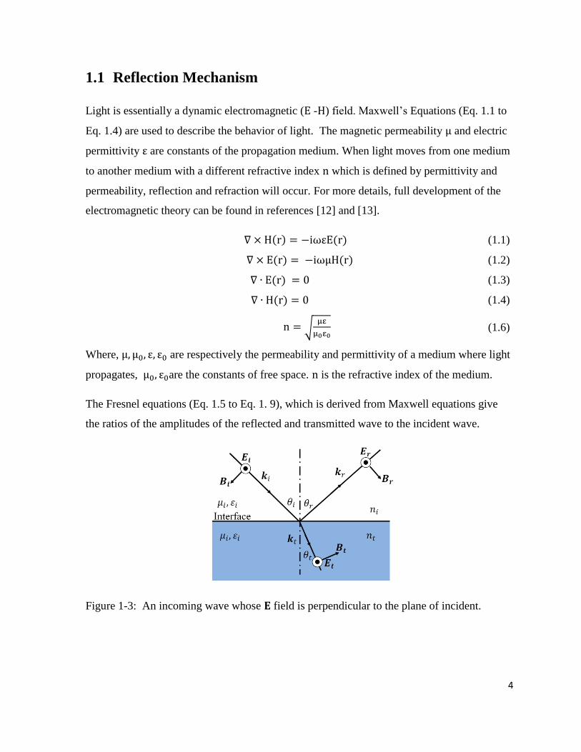
The Fresnel equations (Eq. 1.5 to Eq. 1. 9), which is derived from Maxwell equations give
the ratios of the amplitudes of the reflected and transmitted wave to the incident wave.
Figure 1-3: An incoming wave whose field is perpendicular to the plane of incident.
5
When field is parallel to the plane of incidence, it is defined as TM mode. When filed is
perpendicular to the plane of incidence (TE mode), depicted in Figure 1-1. The
corresponding reflection ratio and amplitude transmission ratio are
(1.7)
(1.8)
for TM mode, is parallel to the plane of incidence,
(1.9)
(1.10)
Where the subscript and denote respectively TM and TE mode.
As a result of the discontinuity of refractive index at material interfaces, a certain amount of
light is reflected. When light shines on multiple layers of material with different thickness,
within one layer of material, the multiple beams of reflection and transmission will interfere
with each other constructively or destructively, as depicted in figure 1-3. For solar cells, the
optical loses between different layers (substrate, photoactive layer, buffer layers) caused a
considerable amount of optical lose due to thin film interference, see figure 1-1(b).
Reflection can be greatly suppressed at each interface by implementing an intermediate
material with gradually varying refractive index in the direction of surface normal.
6
Figure 1-4: A schematic of thin film interference
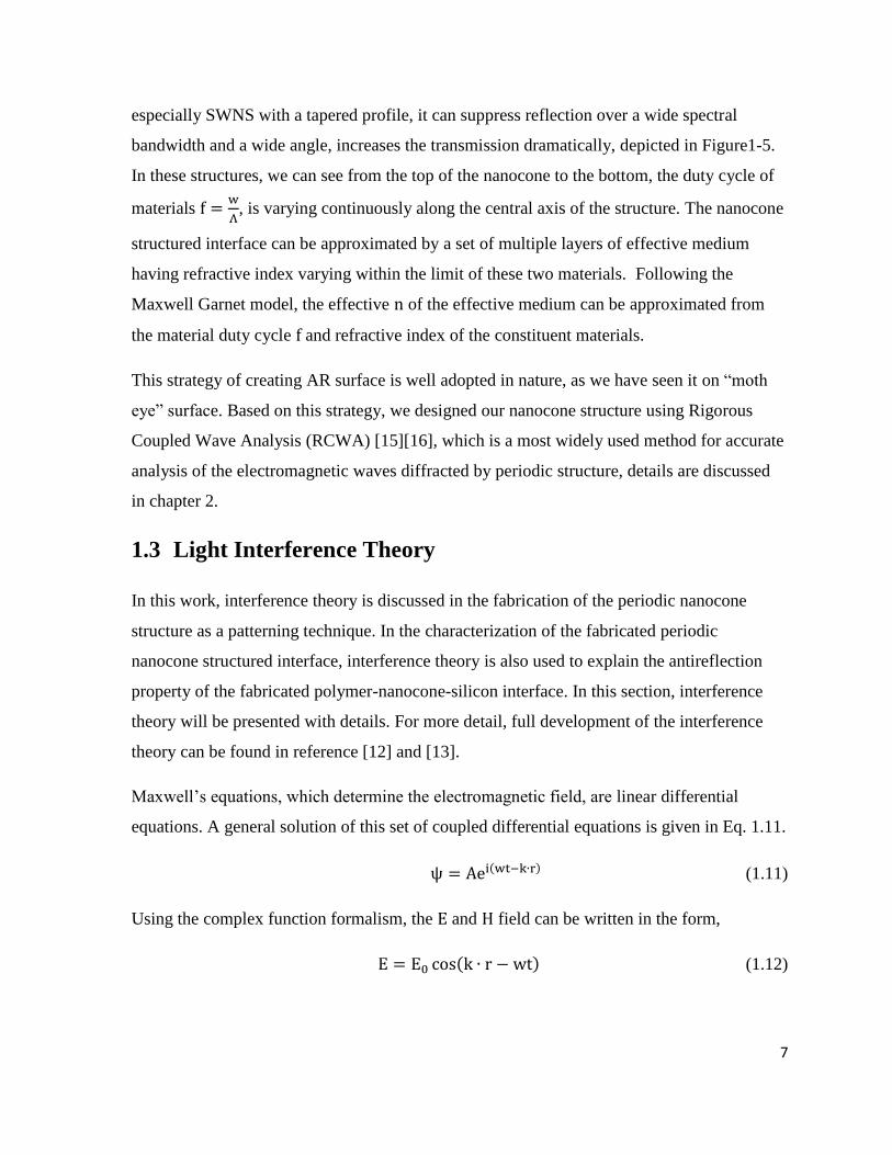
1.2 Periodic Nanocone Structured Solid-Solid Interface
Conventional method of reducing reflection includes single layer thin film coating,
multilayer coating, gradient refractive index coating. Single AR thin film coating is a layer
of low refractive index material with a thickness of a quarter incident wavelength and this
method is very limited by low index materials available. Multilayer AR coating can decrease
the reflection effectively at a particular target wavelength, but will simultaneous increase
reflection efficiency on both sides [14].
Figure 1-5: Subwavelength nanocone structured (a) air-solid interface (b) solid-solid
interface.
When a surface has macroscopic roughness, the light impinges on this kind of surface will
reflect and diffuse, however, when light incident on a surface/interface constructed by SWNS,
7
especially SWNS with a tapered profile, it can suppress reflection over a wide spectral
bandwidth and a wide angle, increases the transmission dramatically, depicted in Figure1-5.
In these structures, we can see from the top of the nanocone to the bottom, the duty cycle of
materials
, is varying continuously along the central axis of the structure. The nanocone
structured interface can be approximated by a set of multiple layers of effective medium
having refractive index varying within the limit of these two materials. Following the
Maxwell Garnet model, the effective of the effective medium can be approximated from
the material duty cycle and refractive index of the constituent materials.
This strategy of creating AR surface is well adopted in nature, as we have seen it on “moth
eye” surface. Based on this strategy, we designed our nanocone structure using Rigorous
Coupled Wave Analysis (RCWA) [15][16], which is a most widely used method for accurate
analysis of the electromagnetic waves diffracted by periodic structure, details are discussed
in chapter 2.
1.3 Light Interference Theory
In this work, interference theory is discussed in the fabrication of the periodic nanocone
structure as a patterning technique. In the characterization of the fabricated periodic
nanocone structured interface, interference theory is also used to explain the antireflection
property of the fabricated polymer-nanocone-silicon interface. In this section, interference
theory will be presented with details. For more detail, full development of the interference
theory can be found in reference [12] and [13].
Maxwell’s equations, which determine the electromagnetic field, are linear differential
equations. A general solution of this set of coupled differential equations is given in Eq. 1.11.
(1.11)
Using the complex function formalism, the and field can be written in the form,
(1.12)
8
where is the angular velocity, is the wave vector and the magnitude of is given by
| |
(1.13)
Irradiance of a beam is defined as the average energy per unit area per unit time, denoted as
(1.14)
Since we are concerned about beam intensity within the same medium, constants are dropped
for simplicity.
(1.15)
Interference is essentially two waves superimpose and form a resultant wave. Two
electromagnetic waves and interfere with each other.
(1.16)
(1.17)
are the magnitude of the field, are the phases, and are respectively the
wave vectors. If is constant, these two waves are said to be in phase.
The result field can be expressed in Eq. 1.18.and the time-averaged intensity distribution
of the interference patterned is given in Eq. 1.19, which are related by the definition of beam
intensity.
(1.18)
| | (1.19)
are respectively the time-averaged intensity of the two incident waves. The third term of
the equation contains information about the mutual coherence of the two waves. If the two
waves are mutually coherent, which means, is constant, the interference pattern is
stationary over time with a spatial period
9
| |
(1.20)
In Eq. 1.20, is the angle of incidence, is the wavelength of the incident light and n is the
refractive index.
From this equation, we know that the period of the interference of two incident light is only
governed by the incident light wavelength, incident angle, and refractive index of the
material.
1.4 Thesis Structure
In this thesis, I present a periodic nanocone structured solid-solid interface in the following
structure. In chapter 2, I used the Rigorous Coupled Wave Analysis to provide a preliminary
design on the periodic nanocone (PNC) structure. Chapter 3 covers the fabrication of the
Polymer-Nanocone-Si interface (PNCSI). Interference lithography mechanism is explained
and characterization results of interference lithography are shown. Multiple steps of Reactive
Ion Etching (RIE) are used to transfer to the pattern into silicon substrate. Chapter 4 explores
the antireflection property of the fabricated PNC at air-solid interface and solid-solid
interface. We also present a model in predicting the antireflection property for PNC at solid-
solid interface based on their antireflection property at air-solid interface. The experimental
and testing results are summarized in Chapter 5.
10
Chapter 2 Design of Periodic Nanocone Structured Solid-
Solid Interface
Over the past 25 years, Rigorous Coupled Wave Analysis (RCWA) has been the most widely
used method for accurate analysis of the diffraction of electromagnetic waves by periodic
structures. The RCWA, a plane wave based analytical method, is a straightforward technique
for obtaining the exact solution of Maxwell’s equations for the electromagnetic diffraction by
grating structures. For the purpose of discussion of PNCSI modeling, a basic review of
RCWA is required. A detailed derivation can be found in [15], [16], [17].
2.1 Rigorous Coupled Wave Analysis Theory
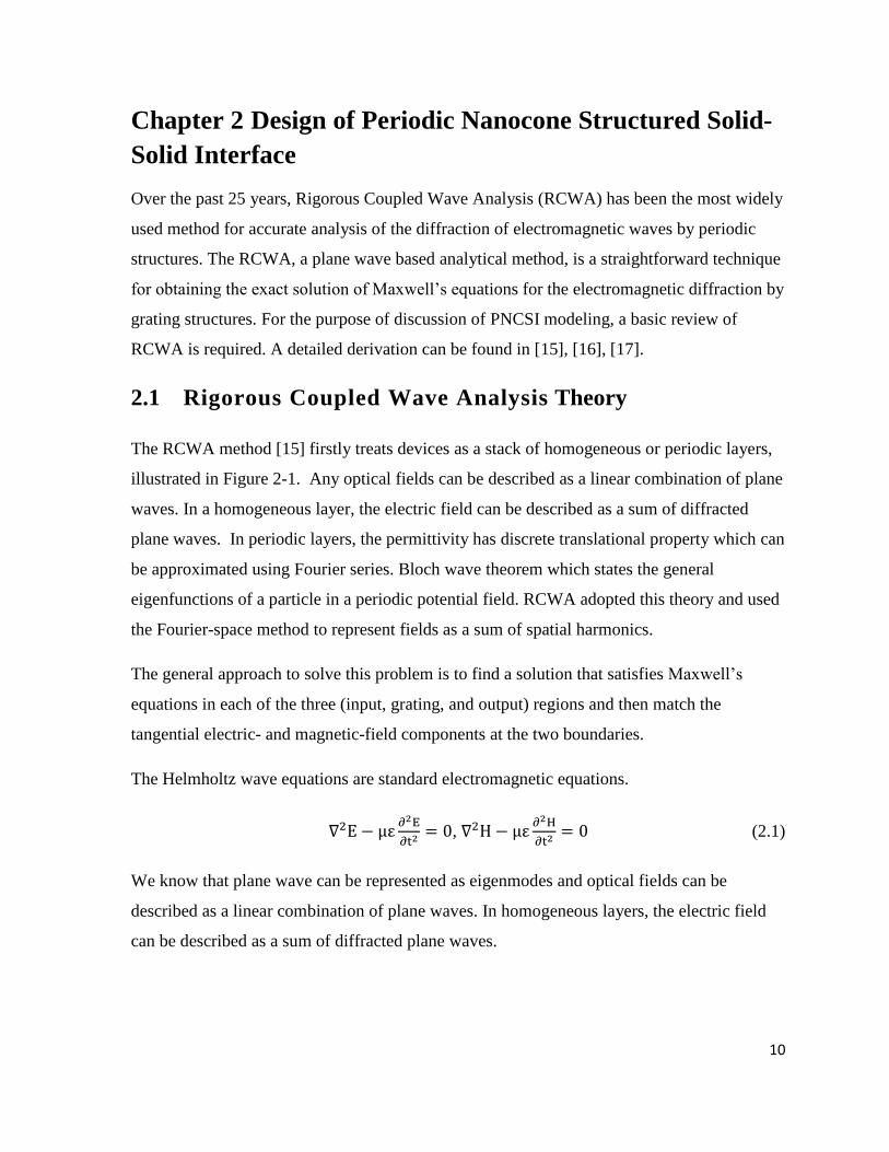
The RCWA method [15] firstly treats devices as a stack of homogeneous or periodic layers,
illustrated in Figure 2-1. Any optical fields can be described as a linear combination of plane
waves. In a homogeneous layer, the electric field can be described as a sum of diffracted
plane waves. In periodic layers, the permittivity has discrete translational property which can
be approximated using Fourier series. Bloch wave theorem which states the general
eigenfunctions of a particle in a periodic potential field. RCWA adopted this theory and used
the Fourier-space method to represent fields as a sum of spatial harmonics.
The general approach to solve this problem is to find a solution that satisfies Maxwell’s
equations in each of the three (input, grating, and output) regions and then match the
tangential electric- and magnetic-field components at the two boundaries.
The Helmholtz wave equations are standard electromagnetic equations.
,
(2.1)
We know that plane wave can be represented as eigenmodes and optical fields can be
described as a linear combination of plane waves. In homogeneous layers, the electric field
can be described as a sum of diffracted plane waves.
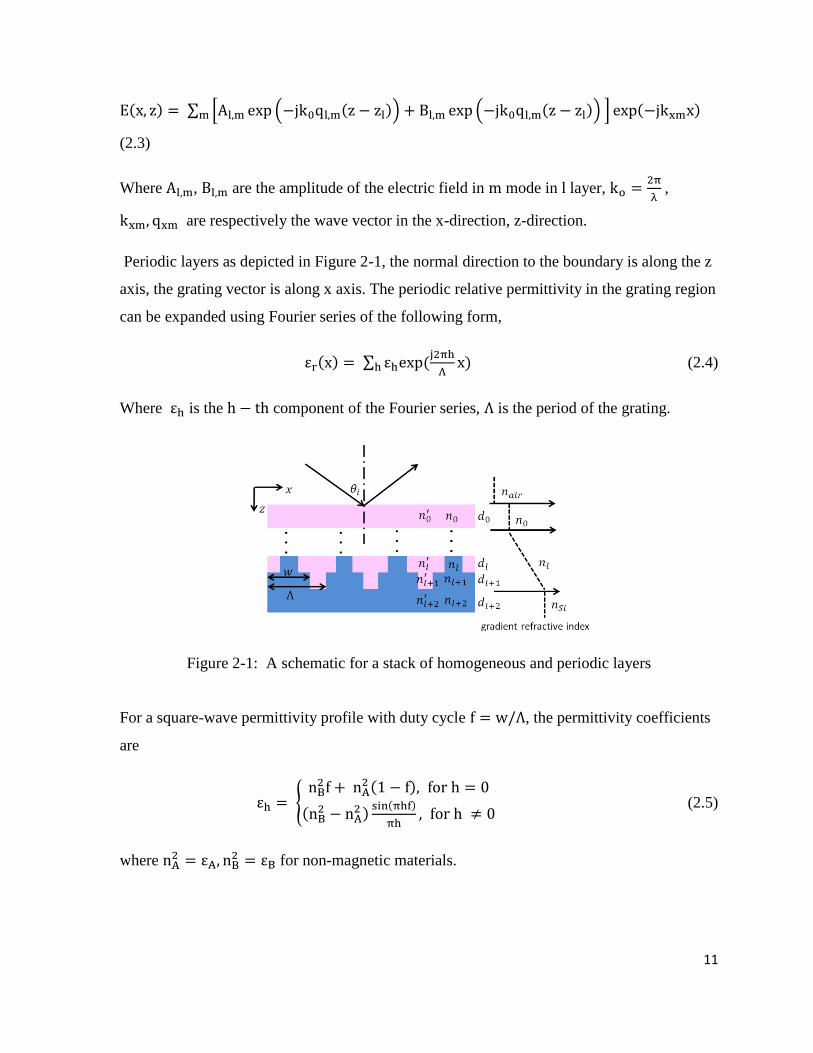
11
∑ [ ( ) ( ) ]
(2.3)
Where , are the amplitude of the electric field in mode in layer,
,
are respectively the wave vector in the x-direction, z-direction.
Periodic layers as depicted in Figure 2-1, the normal direction to the boundary is along the z
axis, the grating vector is along x axis. The periodic relative permittivity in the grating region
can be expanded using Fourier series of the following form,
∑
(2.4)
Where is the component of the Fourier series, is the period of the grating.
Figure 2-1: A schematic for a stack of homogeneous and periodic layers
For a square-wave permittivity profile with duty cycle , the permittivity coefficients
are
{
(2.5)
where
for non-magnetic materials.
12
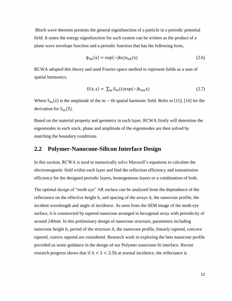
Bloch wave theorem presents the general eigenfunction of a particle in a periodic potential
field. It states the energy eigenfunction for such system can be written as the product of a
plane wave envelope function and a periodic function that has the following form,
(2.6)
RCWA adopted this theory and used Fourier-space method to represent fields as a sum of
spatial harmonics.
∑ (2.7)
Where is the amplitude of the spatial harmonic field. Refer to [15], [16] for the
derivation for .
Based on the material property and geometry in each layer, RCWA firstly will determine the
eigenmodes in each stack, phase and amplitude of the eigenmodes are then solved by
matching the boundary conditions.
2.2 Polymer-Nanocone-Silicon Interface Design
In this section, RCWA is used to numerically solve Maxwell’s equations to calculate the
electromagnetic field within each layer and find the reflection efficiency and transmission
efficiency for the designed periodic layers, homogeneous layers or a combination of both.
The optimal design of “moth eye” AR surface can be analyzed from the dependence of the
reflectance on the effective height , and spacing of the arrays , the nanocone profile, the
incident wavelength and angle of incidence. As seen from the SEM image of the moth eye
surface, it is constructed by tapered nanocone arranged in hexagonal array with periodicity of
around 240nm. In this preliminary design of nanocone structure, parameters including
nanocone height , period of the structure , the nanocone profile, linearly tapered, concave
tapered, convex tapered are considered. Research work in exploring the best nanocone profile
provided us some guidance in the design of our Polymer-nanocone-Si interface. Recent
research progress shows that if at normal incidence, the reflectance is
13
essentially less than 0.5%[18]. Three nanocone structure is proposed [3], “Gaussian-bell
shaped”, “parabola shaped” and linear nanocone and research shows that paraboloidal-shape
nanocone yield a nearly linear refractive index gradient and paraboloidal-shaped nanocone
shows a better antireflection performance.
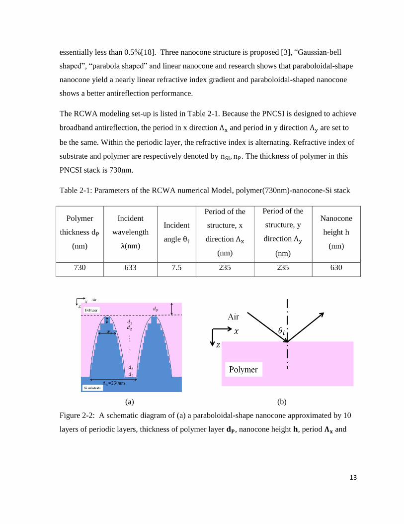
The RCWA modeling set-up is listed in Table 2-1. Because the PNCSI is designed to achieve
broadband antireflection, the period in x direction and period in y direction are set to
be the same. Within the periodic layer, the refractive index is alternating. Refractive index of
substrate and polymer are respectively denoted by . The thickness of polymer in this
PNCSI stack is 730nm.
Table 2-1: Parameters of the RCWA numerical Model, polymer(730nm)-nanocone-Si stack
Polymer
thickness
(nm)
Incident
wavelength
(nm)
Incident
angle
Period of the
structure, x
direction
(nm)
Period of the
structure, y
direction
(nm)
Nanocone
height
(nm)
730 633 7.5 235 235 630
(a) (b)
Figure 2-2: A schematic diagram of (a) a paraboloidal-shape nanocone approximated by 10
layers of periodic layers, thickness of polymer layer , nanocone height , period and
14
, referactive index of polymer, silicon are respectively (b) reflection at a semi-
infinite air and semi-infinite polymer stack.
The duty cycle along the x and y direction, denoted as and are designed to be the same.
The refractive index of the two material within each layer is denoted as and . In this case,
and are respectively index of silicon and polymer . A layer of polymer with
refractive index of 1.65 is spin-coated on top the PNC, creating the PNCSI. The details of
the polymer-nanocone-Si stack are listed in Table 2-2.
Table 2-2: The stack design for the PNC interface with paraboloidal-shaped nanocone
Layer
number
duty cycle in
x direction,
duty cycle in
y direction,
Thickness
(nm)
0 1.65 - - 730
1 1.65 0.26 0.26 31.5
2 1.65 0.36 0.36 31.5
3 1.65 0.45 0.45 31.5
4 1.65 0.52 0.52 31.5
5 1.65 0.57 0.57 31.5
6 1.65 0.63 0.63 31.5
7 1.65 0.68 0.68 31.5
8 1.65 0.73 0.73 31.5
9 1.65 0.78 0.78 31.5
As seen in Figure 1-5(b), the total reflection is a summation of the reflection from air-
polymer interface and PNCSI. In order to show the antireflection performance at PNCSI, we
also calculated the reflection efficiency for a semi-infinite air and semi-infinite polymer stack.
15
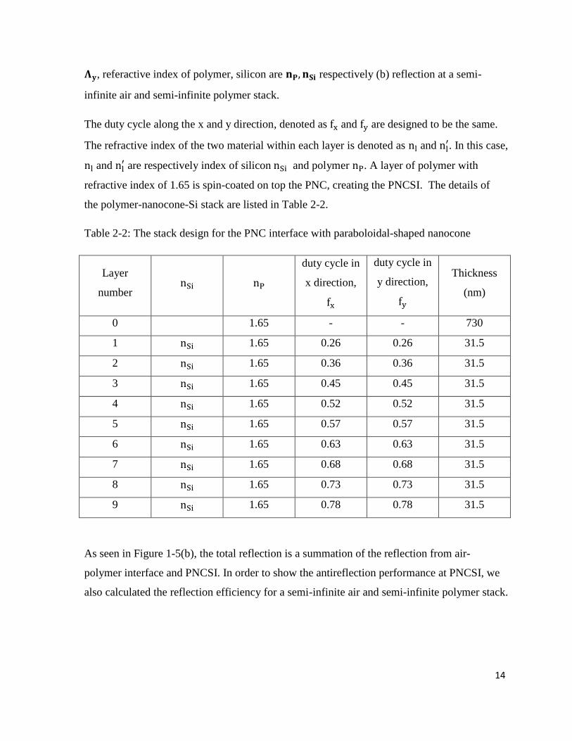
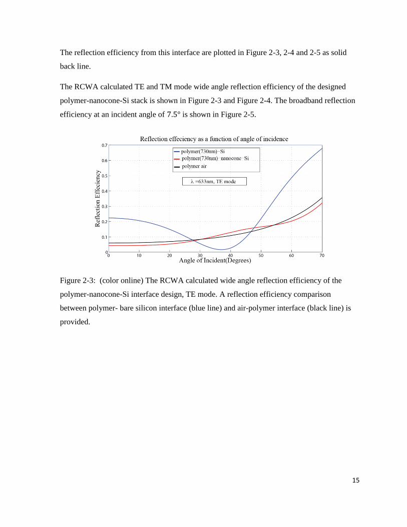
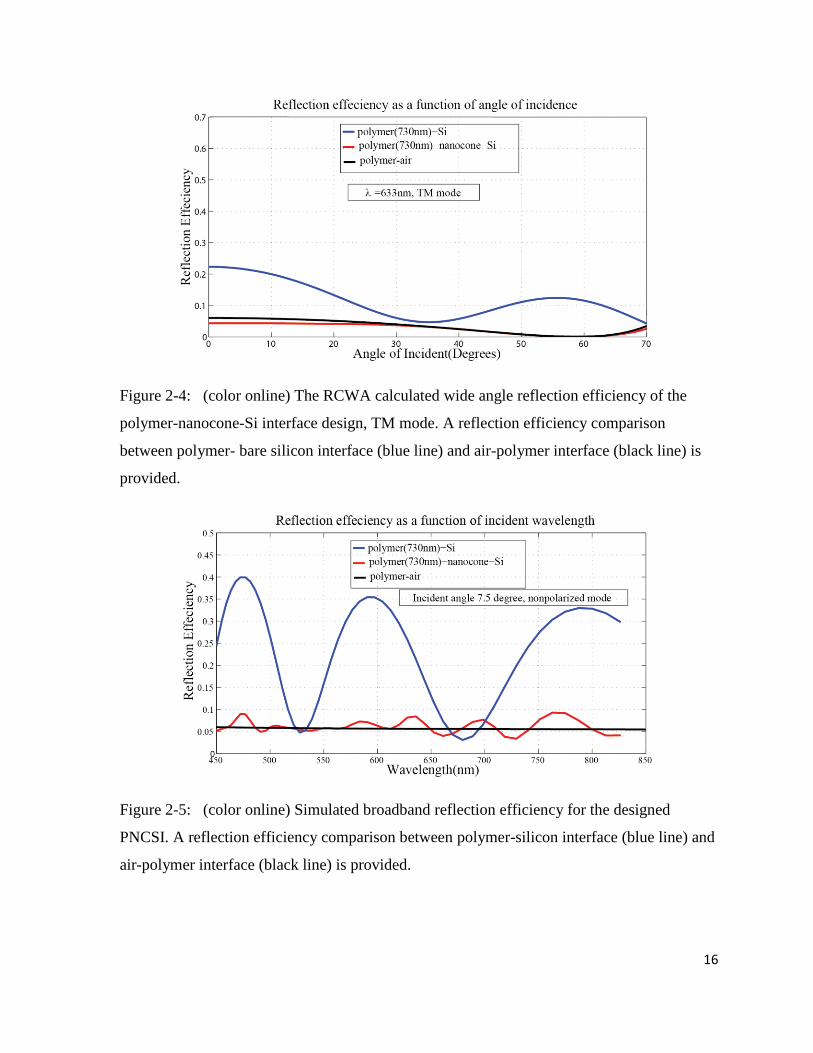
The reflection efficiency from this interface are plotted in Figure 2-3, 2-4 and 2-5 as solid
back line.
The RCWA calculated TE and TM mode wide angle reflection efficiency of the designed
polymer-nanocone-Si stack is shown in Figure 2-3 and Figure 2-4. The broadband reflection
efficiency at an incident angle of is shown in Figure 2-5.
Figure 2-3: (color online) The RCWA calculated wide angle reflection efficiency of the
polymer-nanocone-Si interface design, TE mode. A reflection efficiency comparison
between polymer- bare silicon interface (blue line) and air-polymer interface (black line) is
provided.
16
Figure 2-4: (color online) The RCWA calculated wide angle reflection efficiency of the
polymer-nanocone-Si interface design, TM mode. A reflection efficiency comparison
between polymer- bare silicon interface (blue line) and air-polymer interface (black line) is
provided.
Figure 2-5: (color online) Simulated broadband reflection efficiency for the designed
PNCSI. A reflection efficiency comparison between polymer-silicon interface (blue line) and
air-polymer interface (black line) is provided.
17
The simulated broadband reflection of Polymer-Si interface has a 35% reflection at
, meanwhile, the designed PNCSI has around 6% reflection from 450nm to750 nm,
which is the range for visible light. The overlap of the reflection efficiency of PNCSI and
air-polymer interface indicates that most of the reflection from PNCSI is a result of the
reflection from air-polymer interface. This shows that the reflection from PNCSI is mostly
eliminated, resulting in overall reduced thin film interference effect. This design provides us
guidance in the periodic nanocone structure fabrication, which is most important functional
component in the polymer-nanocone-Si interface.
18
Chapter 3 Fabrication of Periodic Nanocone Structured
Solid-Solid Interface
Different methods have been investigated to fabricate antireflection surface and mainly
classified into bottom up fabrication and top down fabrication. Bottom up fabrication
methods such as physical vapor deposition and chemical vapor deposition have been used to
deposit porous films with decreasing density, correspondingly higher porosity, eventually
resulting in lower refractive index [2]. However, this method is very limited by materials and
thus the application in eliminating reflection from solid-solid interface is very limited.
Whereas, polymer-nanocone-Si interface structurally creates an intermediate layer with a
continuous gradient refractive index. In our work, firstly, interference lithography (IL) and
steps of reactive ion etching (RIE) are used to create the periodic nanocone structure and
polymer is spin-coated in the last step to create the polymer-nanocone-Si interface.
IL is a patterning method that can create large area of periodic structure with a very high
spatial-phase coherence. Masked dry etching will give a better control over the overall
structure geometry. The mask aperture and period control the lateral cross section, whereas
the etch rate control the longitudinal height of the nanostructures. In this case, the fabrication
method provides great flexibility in optimizing the nanocone profile in the future.
3.1 Laser Interference Lithography
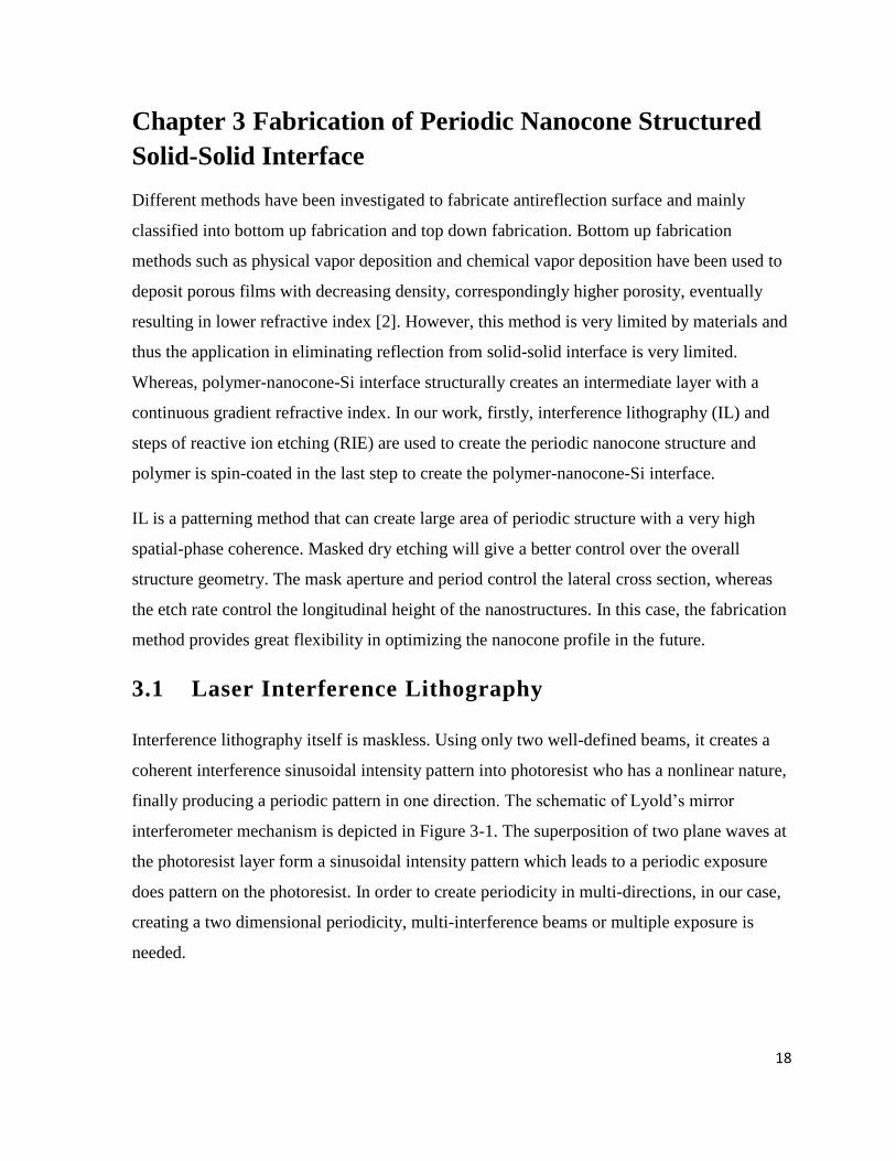
Interference lithography itself is maskless. Using only two well-defined beams, it creates a
coherent interference sinusoidal intensity pattern into photoresist who has a nonlinear nature,
finally producing a periodic pattern in one direction. The schematic of Lyold’s mirror
interferometer mechanism is depicted in Figure 3-1. The superposition of two plane waves at
the photoresist layer form a sinusoidal intensity pattern which leads to a periodic exposure
does pattern on the photoresist. In order to create periodicity in multi-directions, in our case,
creating a two dimensional periodicity, multi-interference beams or multiple exposure is
needed.
19
(a) (b)
Figure 3-1: a schematic diagram of interference lithography
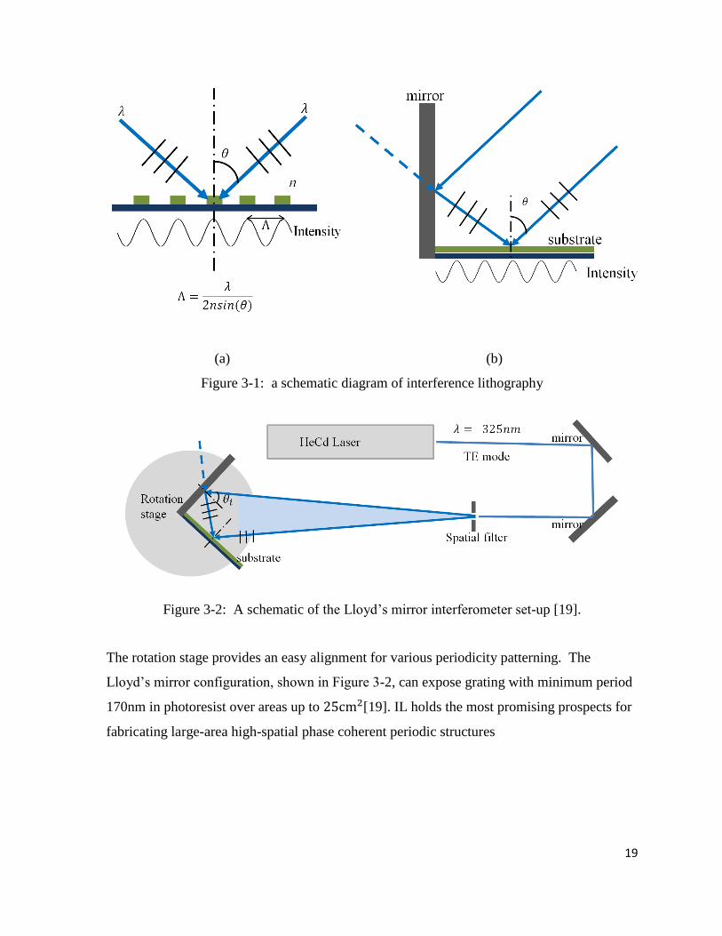
Figure 3-2: A schematic of the Lloyd’s mirror interferometer set-up [19].
The rotation stage provides an easy alignment for various periodicity patterning. The
Lloyd’s mirror configuration, shown in Figure 3-2, can expose grating with minimum period
170nm in photoresist over areas up to [19]. IL holds the most promising prospects for
fabricating large-area high-spatial phase coherent periodic structures
20
3.2 Interference Lithography Stack Design
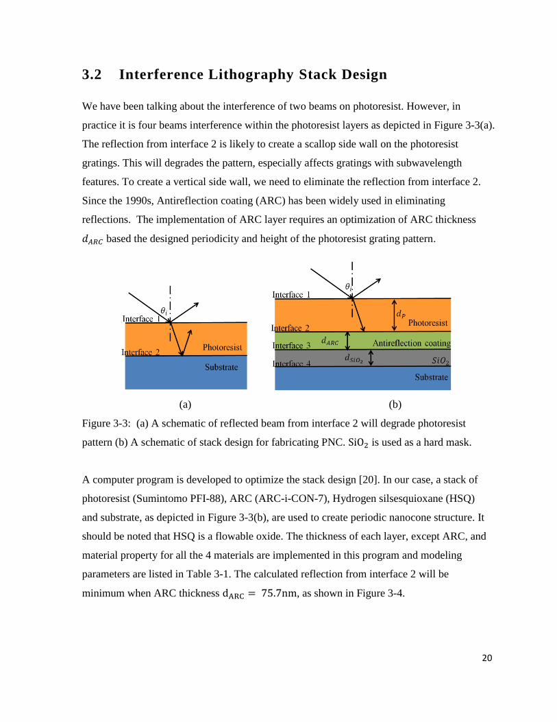
We have been talking about the interference of two beams on photoresist. However, in
practice it is four beams interference within the photoresist layers as depicted in Figure 3-3(a).
The reflection from interface 2 is likely to create a scallop side wall on the photoresist
gratings. This will degrades the pattern, especially affects gratings with subwavelength
features. To create a vertical side wall, we need to eliminate the reflection from interface 2.
Since the 1990s, Antireflection coating (ARC) has been widely used in eliminating
reflections. The implementation of ARC layer requires an optimization of ARC thickness
based the designed periodicity and height of the photoresist grating pattern.
(a) (b)
Figure 3-3: (a) A schematic of reflected beam from interface 2 will degrade photoresist
pattern (b) A schematic of stack design for fabricating PNC. is used as a hard mask.
A computer program is developed to optimize the stack design [20]. In our case, a stack of
photoresist (Sumintomo PFI-88), ARC (ARC-i-CON-7), Hydrogen silsesquioxane (HSQ)
and substrate, as depicted in Figure 3-3(b), are used to create periodic nanocone structure. It
should be noted that HSQ is a flowable oxide. The thickness of each layer, except ARC, and
material property for all the 4 materials are implemented in this program and modeling
parameters are listed in Table 3-1. The calculated reflection from interface 2 will be
minimum when ARC thickness , as shown in Figure 3-4.
21
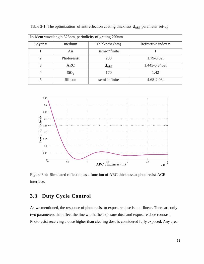
Table 3-1: The optimization of antireflection coating thickness parameter set-up
Incident wavelength 325nm, periodicity of grating 200nm
Layer # medium Thickness (nm) Refractive index
1 Air semi-infinite 1
2 Photoresist 200 1.79-0.02i
3 ARC 1.445-0.3402i
4 170 1.42
5 Silicon semi-infinite 4.68-2.03i
Figure 3-4: Simulated reflection as a function of ARC thickness at photoresist-ACR
interface.
3.3 Duty Cycle Control
As we mentioned, the response of photoresist to exposure dose is non-linear. There are only
two parameters that affect the line width, the exposure dose and exposure dose contrast.
Photoresist receiving a dose higher than clearing dose is considered fully exposed. Any area
22
receiving a dose lower than clearing dose is underexposed. In the case of positive photoresist,
exposed area will be removed by developer, resulting in periodic grating structures. The line
width is defined as the width of the ridge. Duty cycle of the structure is defined as
.
The intensity pattern of the interference is sinusoidal. The contrast is defined as
(3.1)
when the contrast is 0, there will be no structure developed on the photoresist. The highest
contrast m = 1, in which , means some area doesn’t receive any exposure. For
negative photoresist, a higher contrast will result in a smaller line width, whereas for positive
resist, will results in larger line width. In practice, perfect contrast is unattainable and it
should be noted that there is the maximum or the minimum line width that is affected by
material properties.
It is apparent that exposure dose is the easier way to control the line width. As shown in
Figure 3-5, by increasing the exposure dose, the line width is decreased.
Figure 3-5: Resist receives an exposure dose higher than clearing dose is considered exposed.
Higher exposure dose will result in a smaller line width in positive photoresist [17].
23
The relationship of duty cycle as a function of exposure dose can be related in Eq. 3.2 [17]
(3.2)
where is the dose that the photoresist is exposed to.
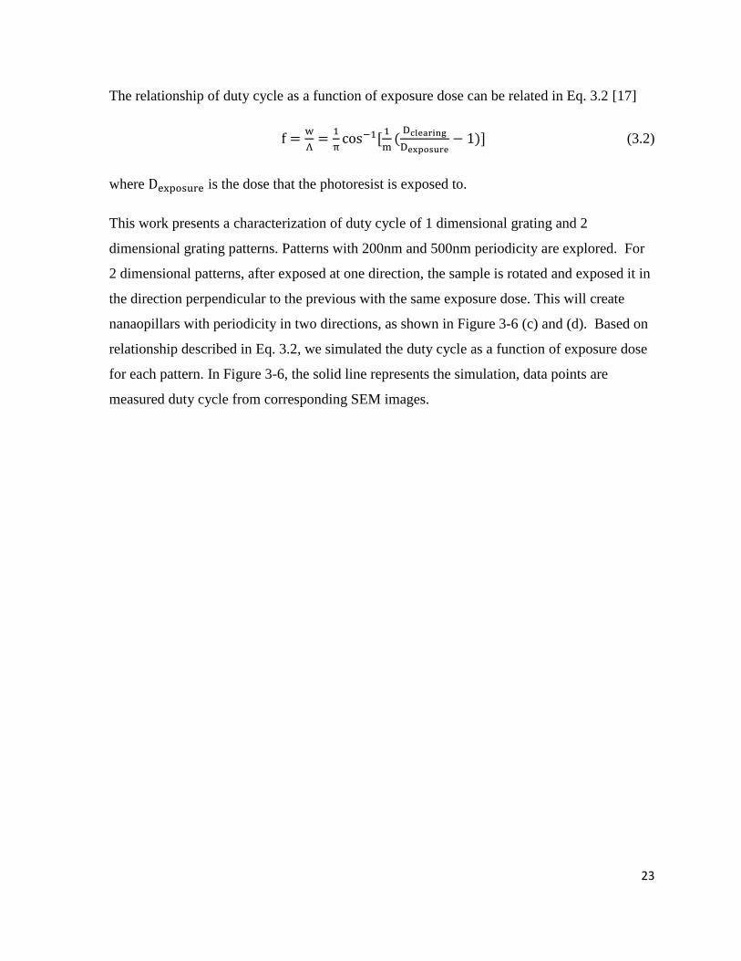
This work presents a characterization of duty cycle of 1 dimensional grating and 2
dimensional grating patterns. Patterns with 200nm and 500nm periodicity are explored. For
2 dimensional patterns, after exposed at one direction, the sample is rotated and exposed it in
the direction perpendicular to the previous with the same exposure dose. This will create
nanaopillars with periodicity in two directions, as shown in Figure 3-6 (c) and (d). Based on
relationship described in Eq. 3.2, we simulated the duty cycle as a function of exposure dose
for each pattern. In Figure 3-6, the solid line represents the simulation, data points are
measured duty cycle from corresponding SEM images.
24
(a) (b)
(c ) (d)
Figure 3-6: Line width as a function of exposure dose for (a) 1 Dimensional (1D) photoresist
grating, photoresist thickness 200nm, periodicity 200nm, (b) 1D photoresist grating,
photoresist thickness 500nm, periodicity 500nm, (c) 2 Dimensional (2D) photoresist grating,
photoresist thickness 200nm, periodicity 200nm, (d) 2D photoresist grating, photoresist
thickness 500nm, periodicity 500nm. The inset micrographs are the corresponding patterns.
25
3.4 Polymer-Nanocone-Si Interface Fabrication Process
In the fabrication of PNCSI interface, dry anisotropic etching is selected because it gives
better control over nanostructure profile compared to wet, isotropic etching. After the pattern
is created, we used RIE to transfer the pattern into ARC layer. Reactive Ion Etching
is used to transfer the photoresist pattern into layer, which is used as a hard mask.
mask is used because the etching selectivity between and is very high. The tapered
nanocone profile is controlled by the mask aperture and the etching selectivity between
and . The mask aperture and period control the nanostructure lateral cross section, whereas
the etching rate controls the longitudinal height of the nanostructures. The etching process
effectively transfers the pattern from photoresist to silicon substrate. A flow chart of the
fabrication process is shown in figure 3-7.
26
(a) HSQ, ARC, Photoresist are spin coated, thickness of each layer is listed in Table 3-1
(b) Photoresist is exposed and developed (c) Etch ARC layer with RIE
(d) Etch layer with RIE (e) Etch substrate with RIE
(f) A layer of polymer is spin coated on top of nanocones
Figure 3-7: The PNCSI fabrication process starts with (a) spin-coat, HSQ, ARC, photoresist
(b) photoresist is exposed and developed, (c) RIE transfer the photoresist pattern into
ARC layer, (d) RIE transfer the pattern into , (e) Etch Silicon with RIE, (f)
27
photoresist is spin- coated on top of the nanocone structures. This process creates the
polymer-nanocone-silicon interface.
The corresponding fabrication results of each step are shown in Figure 3-8, Figure 3-9 and
Figure 3-10,.
(a) (b) (c)
Figure 3-8: Photoresist is exposed and developed. (A) A titled view of the edge of the
pattern, (b) top view of the photoresist pattern, (c) a zoomed-in image of the 2D grating
pattern. The scale bar is shown in each figure.
(a) (b) (c)
Figure 3-9 : 2D-200nm periodicity pattern after 1.8min RIE (A) A titled view of the
edge of the sample, (b) top view after RIE, (c) a zoomed-in image of the top surface.
400nm
230nm
𝜇𝑚 𝜇𝑚
28
(a) (b)
Figure 3-10: 2D-200nm periodicity pattern after 1.8min RIE and 10.5min RIE (A) a
tilted view of the edge after RIE , (b) top view after RIE, (c) a zoomed-in
image of the top surface.
The antireflection property of nanocone structured interface depends on nanocone height,
spacing, nanocone profiles. The following figures shows how the etching time affects the
height and profile of the nanocone structure. As it is shown, the RIE 12min will not only
increase the height of nanocone, but also shape the cone with a near paraboloidal profile.
(a) (b) (c)
Figure 3-11: A tilted view of the surface of the 2D-200nm pattern after 1.8min RIE
and 10.5min RIE and (a) 5min RIE (b) 8min RIE (c) 12min RIE.
400nm 𝜇𝑚
500nm 500nm 500nm
29
Table 3-2: Reactive ion etching parameters for 2D-200nm period pattern transfer process
Pressure
(mT)
Flow rate
(Sccm)
Power
(W)
Time
(min) Etch Rate (nm/min)
RIE 20 15 54 1.8 37
RIE 30 15 89 10.5 15
RIE 5 30 100 13 50
In order to further characterize the antireflection property of the PNCSI, we fabricated a set
of sample which are numbered from 1 to 5. The SEM images of the nanocone structure for
sample 2 to 5 are shown in Figure 3-12.
30
(a) (b)
(c) (d)
Figure 3-12: Micrographs of tilted views of the surface of periodic nanocone structure
between air and silicon substrate with the same spacing, but different height and profiles (a)
sample 2 450 (b) sample 3, (c) sample 4, (d) sample 5,
In the last step, we coated the samples with polymer which has a refractive index,
at wavelength of 633nm.
500nm 500nm
500nm 500nm
31
(a) (b)
Figure 3-13: Micrographs of the fabricated Polymer-nanocone-Si interface. (a) A titled
view of 230nm periodic nanocone constructed interface between polymer and silicon
substrate. (b) A zoomed-in micrograph of PNCSI with nanocone structure ( ) and
polymer ( ).
The antireflection property can clearly be observed from Figure 3-14. The sample size is
. The samples are placed in front of a LED screen. The PNCSI sample greatly
suppressed the reflection compared to bare silicon wafer and silicon wafer coated with
1230nm polymer.
Figure 3-14: Images of (a) Polymer-nanocone-Si sample , (b) bare silicon coated with
1320nm polymer and (c) Bare silicon wafer.
𝜇𝑚
Polymer
PNCSI
Si
𝜇𝑚
(a) (b) (c)
32
Chapter 4 Polymer-Nanocone-Si Interface Antireflection
Characterization
In the previous chapter, we have addressed the design and fabrication of nanocone structured
surface related problems. We introduced the RCWA tool in designing the nanocone structure.
In the fabrication process, we used Lloyd’s interferometer to pattern the photoresist and
achieved high accuracy of line width control. In the pattern transfer process, we used
, RIE sequentially. Periodic nanocone structure with an aspect ratio of 3.2 is
fabricated and later on coated with a layer of polymer with a thickness of
(sample 1). Meanwhile, in order to provide a good comparison, we prepared polymer coated
bare silicon samples. They are bare silicon coated with a layer of 1320nm thickness polymer,
and bare silicon coated with thickness polymer.
In this chapter, firstly, we will present the characterization of the antireflection performance
of the samples and provide wide angle and broadband reflection efficiency measurement
results to validate the RCWA reflection efficiency calculations. Secondly, we will present a
contrast model to predict the antireflection property of nanocone structured solid-solid
interface based on the air-nanocone-Si antireflection property. This model will provide very
good guidance in designing PNCSIs and estimating optoelectronics device performance
which integrated with PNCSIs.
4.1 RCWA based Polymer-nanocone-Si Interface Modeling
In the RCWA model, the subwavelength nanocone structure is modeled as 20 discrete
periodic layers with duty cycle varying in both x and y direction varying. The general
parameter set-up in RCWA model is listed in Table 4-1. The parameters in the model
correspond very closely to the actual dimensions of the nanocone structures and the
dispersion of silicon and polymer are considered in the RCWA calculations.
In the RCWA modeling for nanocone structured surface, a stack of 20 layers is used to
approximate the nanocone structure, see Table 4-2, where , are respectively the
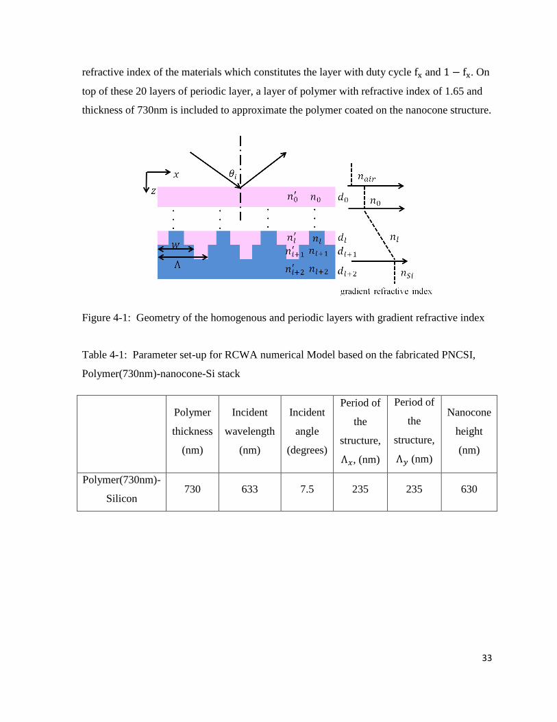
33
refractive index of the materials which constitutes the layer with duty cycle and . On
top of these 20 layers of periodic layer, a layer of polymer with refractive index of 1.65 and
thickness of 730nm is included to approximate the polymer coated on the nanocone structure.
Figure 4-1: Geometry of the homogenous and periodic layers with gradient refractive index
Table 4-1: Parameter set-up for RCWA numerical Model based on the fabricated PNCSI,
Polymer(730nm)-nanocone-Si stack
Polymer
thickness
(nm)
Incident
wavelength
(nm)
Incident
angle
(degrees)
Period of
the
structure,
, (nm)
Period of
the
structure,
(nm)
Nanocone
height
(nm)
Polymer(730nm)-
Silicon 730 633 7.5 235 235 630
34
Table 4-2 : Parameters set-up in RCWA model for the approximation of the fabricated
PNCSI
Layer
number
duty cycle in
x direction,
duty cycle in
y direction,
Thickness
(nm)
0 - 1.65 - - 730
1 1.65 0 0 31.5
2 1.65 0.01 0.01 31.5
3 1.65 0.02 0.02 31.5
4 1.65 0.04 0.04 31.5
5 1.65 0.08 0.08 31.5
6 1.65 0.11 0.11 31.5
7 1.65 0.23 0.23 31.5
8 1.65 0.32 0.32 31.5
9 1.65 0.35 0.35 31.5
10 1.65 0.39 0.39 31.5
11 1.65 0.42 0.42 31.5
12 1.65 0.45 0.45 31.5
13 1.65 0.48 0.48 31.5
14 1.65 0.52 0.52 31.5
15 1.65 0.57 0.57 31.5
16 1.65 0.63 0.63 31.5
17 1.65 0.66 0.66 31.5
18 1.65 0.69 0.69 31.5
19 1.65 0.73 0.73 31.5
20 1.65 0.78 0.78 31.5
35
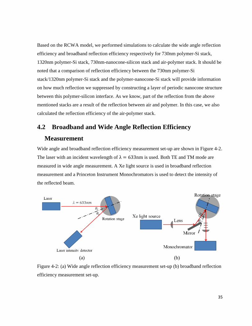
Based on the RCWA model, we performed simulations to calculate the wide angle reflection
efficiency and broadband reflection efficiency respectively for 730nm polymer-Si stack,
1320nm polymer-Si stack, 730nm-nanocone-silicon stack and air-polymer stack. It should be
noted that a comparison of reflection efficiency between the 730nm polymer-Si
stack/1320nm polymer-Si stack and the polymer-nanocone-Si stack will provide information
on how much reflection we suppressed by constructing a layer of periodic nanocone structure
between this polymer-silicon interface. As we know, part of the reflection from the above
mentioned stacks are a result of the reflection between air and polymer. In this case, we also
calculated the reflection efficiency of the air-polymer stack.
4.2 Broadband and Wide Angle Reflection Efficiency
Measurement
Wide angle and broadband reflection efficiency measurement set-up are shown in Figure 4-2.
The laser with an incident wavelength of is used. Both TE and TM mode are
measured in wide angle measurement. A Xe light source is used in broadband reflection
measurement and a Princeton Instrument Monochromators is used to detect the intensity of
the reflected beam.
(a) (b)
Figure 4-2: (a) Wide angle reflection efficiency measurement set-up (b) broadband reflection
efficiency measurement set-up.
36
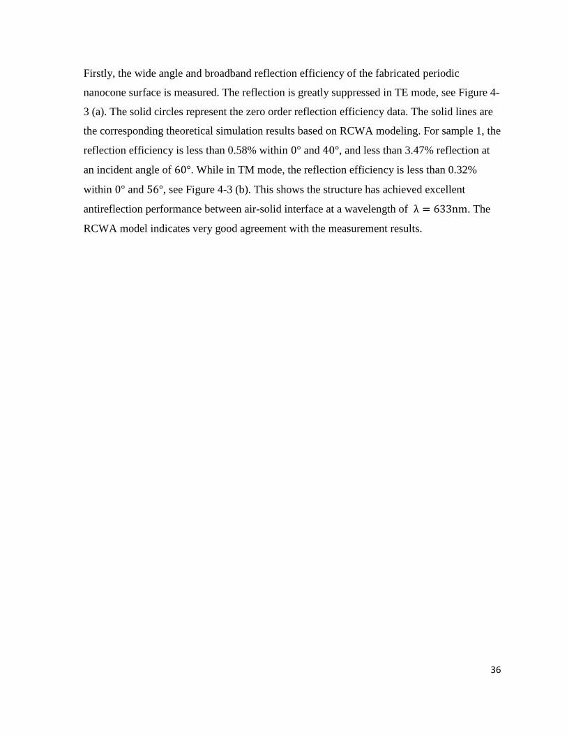
Firstly, the wide angle and broadband reflection efficiency of the fabricated periodic
nanocone surface is measured. The reflection is greatly suppressed in TE mode, see Figure 4-
3 (a). The solid circles represent the zero order reflection efficiency data. The solid lines are
the corresponding theoretical simulation results based on RCWA modeling. For sample 1, the
reflection efficiency is less than 0.58% within and , and less than 3.47% reflection at
an incident angle of . While in TM mode, the reflection efficiency is less than 0.32%
within and , see Figure 4-3 (b). This shows the structure has achieved excellent
antireflection performance between air-solid interface at a wavelength of . The
RCWA model indicates very good agreement with the measurement results.
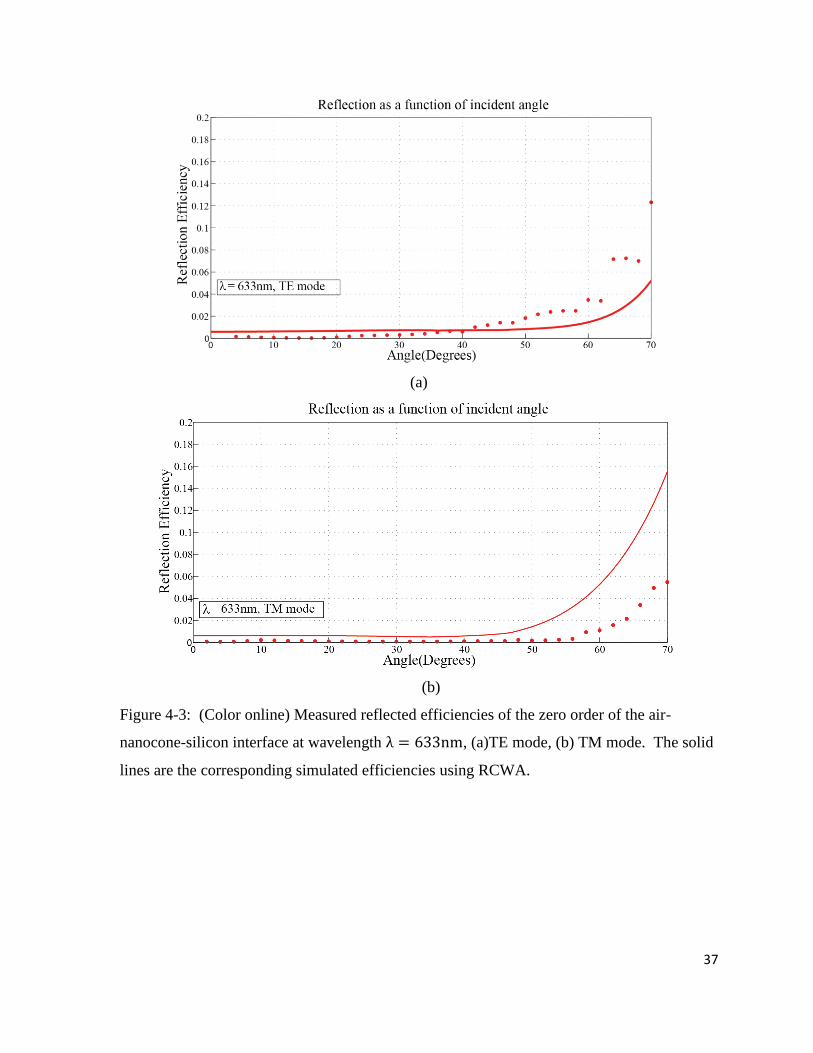
37
(a)
(b)
Figure 4-3: (Color online) Measured reflected efficiencies of the zero order of the air-
nanocone-silicon interface at wavelength , (a)TE mode, (b) TM mode. The solid
lines are the corresponding simulated efficiencies using RCWA.
38
(a)
(b)
Figure 4-4: Measured reflected efficiencies of the zero order of PNCSI integrated sample 1-5
at incident wavelength , (a)TE mode, (b) TM mode.
The antireflection performance of the fabricated PNCSI at solid-solid interface is also
characterized using wide angle and broadband measurement. Figure 4-5, (a) and (b) show the
RCWA calculation has very good agreement with measured wide angle reflection
𝜆
𝜆
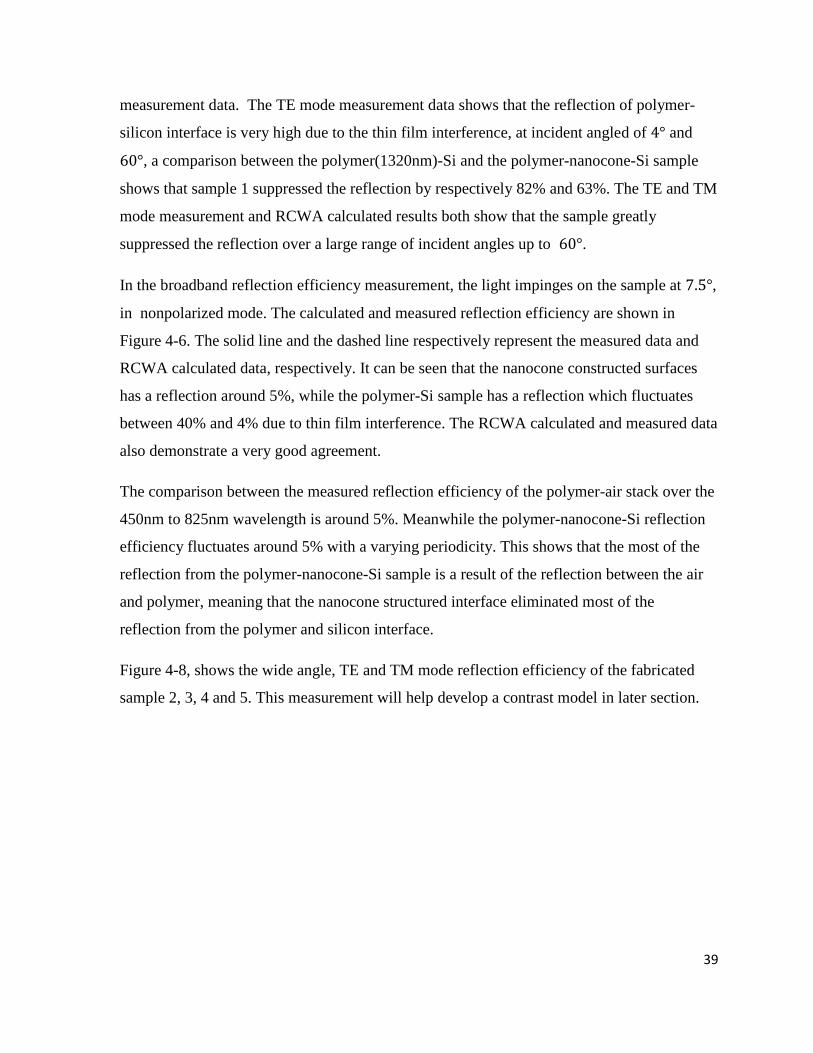
39
measurement data. The TE mode measurement data shows that the reflection of polymer-
silicon interface is very high due to the thin film interference, at incident angled of and
, a comparison between the polymer(1320nm)-Si and the polymer-nanocone-Si sample
shows that sample 1 suppressed the reflection by respectively 82% and 63%. The TE and TM
mode measurement and RCWA calculated results both show that the sample greatly
suppressed the reflection over a large range of incident angles up to .
In the broadband reflection efficiency measurement, the light impinges on the sample at ,
in nonpolarized mode. The calculated and measured reflection efficiency are shown in
Figure 4-6. The solid line and the dashed line respectively represent the measured data and
RCWA calculated data, respectively. It can be seen that the nanocone constructed surfaces
has a reflection around 5%, while the polymer-Si sample has a reflection which fluctuates
between 40% and 4% due to thin film interference. The RCWA calculated and measured data
also demonstrate a very good agreement.
The comparison between the measured reflection efficiency of the polymer-air stack over the
450nm to 825nm wavelength is around 5%. Meanwhile the polymer-nanocone-Si reflection
efficiency fluctuates around 5% with a varying periodicity. This shows that the most of the
reflection from the polymer-nanocone-Si sample is a result of the reflection between the air
and polymer, meaning that the nanocone structured interface eliminated most of the
reflection from the polymer and silicon interface.
Figure 4-8, shows the wide angle, TE and TM mode reflection efficiency of the fabricated
sample 2, 3, 4 and 5. This measurement will help develop a contrast model in later section.
40
(a)
(b)
Figure 4-5: (Color online) Measured reflected efficiencies of the zero order of the nanocone
structured surface, silicon coated with 1320nm polymer and silicon coated with 730nm
polymer under incident wavelength , (a) TE mode, (b) TM mode. The solid lines
are the corresponding simulated efficiencies using RCWA.
41
Figure 4-6: (Color online) Measured reflected efficiencies of the polymer-nanocone-Si
interface, 730nm polymer-Si interface, 1320nm-Polymer-Si interface, at an incident angle
The solid lines are measured data and the dotted line are the corresponding simulated
efficiencies using RCWA.
As it can be seen in Figure 4-6, the measured reflection efficiency fluctuates around 2% in a
close sinusoidal form across 450nm and 825nm wavelength due to the thin interference.
From this sinusoidal reflection efficiency, we will be able to calculate the reflection only
from the nanocone-polymer interface. Obtaining the information, it will help us examine how
the reflection from the polymer-nanocone interface affects the overall reflection.
42
4.3 Reflection Efficiency Contrast Model
The ability to distinguish the high- and low-intensity regions can be quantified with a
parameter m, known as contrast, or visibility, as defined in Eq. 4.1.
(4.1)
or
(4.2)
where are the maximum and minimum intensity respectively, and are
respectively the amplitude of the two incident wave.
From the broadband reflection efficiency measurement of the fabricated PNCSI, we are able
to calculate the contrast. The contrast of the reflection efficiency over a broadband is not
spatial beam interference. The contrast presented here is a function of wavelength. It can also
be expressed as
(4.3)
where are the time-averaged intensities of the two incident wave. Since the these two
beams are mutually in phase, the interference pattern has a period given by,
| |
(4.4)
In Eq. 4.4, is the angle of incident, is the wavelength of the incident light. Since varies,
so is the periodicity, as shown in Figure 4-6.
In this section, we will present a model to predict the contrast of reflection efficiency of any
coating-nanocone-substrate interface based on the antireflection performance of the structure
at the air-nanocone interface. This model will help examine how the reflection from the
43
coating-nanocone interface affects the overall reflection efficiency, thus providing guidance
to achieve best antireflection performance in multi-layered devices.
Figure 4-7: A schematic of (a) reflection at air-nanocone interface is suppressed, (b)
beam interference in polymer-nanocone-substrate stack. The reflection from polymer-
nanocone interface interfere with reflection from air-polymer interface .
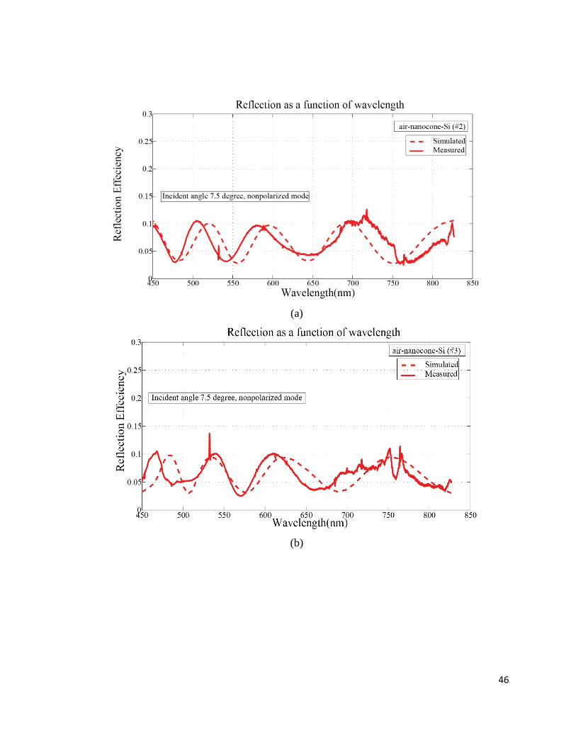
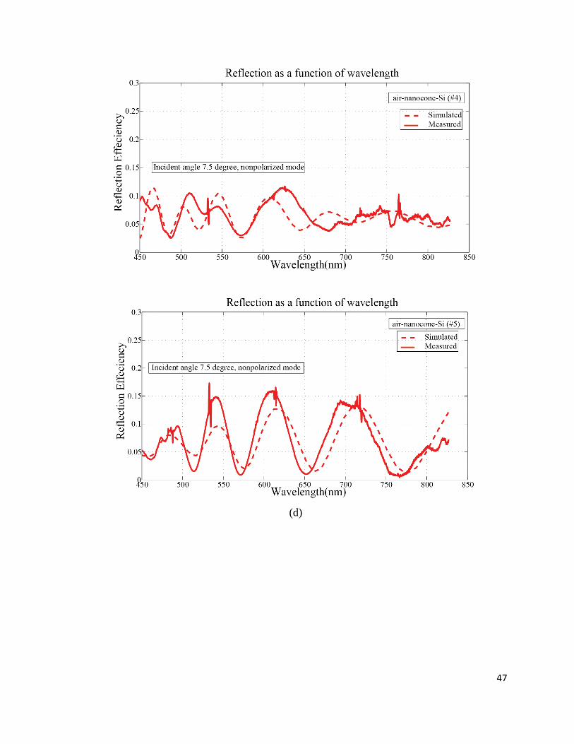
To characterize the contrast as a function of reflection efficiency of A2, we fabricated a 4
more sample, shown in Figure 3-12. The broadband measurement results of sample 2 to 5 are
shown in Figure 4-8 (a) to (d). As it is shown, sample 4 has the highest cone structure,
however the antireflection in broadband is not as good as sample 1. However it achieves a
much better antireflection performance at longer and near infrared wavelength This is a result
of the nanocone height. A characterization of the antireflection performance dependence on
nanocone geometry, height, and cone profile will be presented in the future.
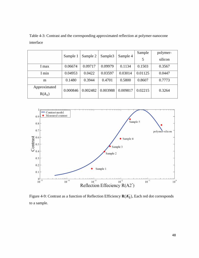
Based on the broadband measurement of sample 1 to 5, we calculated the contrast for each
of them. For example, sample 1, using the measured reflectance efficiency data from PNCSI,
. . The contrast . Setting and
in Eq. 4.2, we will have 0.0744, see Table 4-3. This shows that the
reflection from the polymer-silicon interface is only 7% of the total reflection from the air-
polymer interface. The contrast of each sample based on broadband measurement is listed in
Table 4-3.
44
Since the reflection at the coating-substrate interface can’t directly be measured,
approximations are used. The refractive index of the polymer that is used in the fabricated
PNCSI is close to 1. The reflection efficiencies of sample 1 to 5 at an incident angle , in
TE mode, are used to approximate the reflection at polymer-nanocone interface. Figure 4-4
shows the TE mode and TM mode wide angle reflection efficiency measurement results. As
shown, the approximated reflection,
, where the
subscript denote the sample number.
Implementing Eq.4.2, and setting to be the reflection between air and polymer, we predict
contrast as a function of R( ). The contrast model is shown in Figure 4-9. The measured
contrast has a very good agreement with the model.
45
Figure 4-8: (Color online) Measured and simulated reflected efficiencies for the fabricated
the polymer-nanocone-Si stack at an incident angle 7.5°, (a) sample 2, (b) sample 3, (c)
sample 4, (d) sample 5. The solid lines are measured data and the dotted line are the
corresponding simulated efficiencies using RCWA.
46
(a)
(b)
47
(d)
48
Table 4-3: Contrast and the corresponding approximated reflection at polymer-nanocone
interface
Sample 1 Sample 2 Sample3 Sample 4 Sample
5
polymer-
silicon
I max 0.06674 0.09717 0.09979 0.1134 0.1503 0.3567
I min 0.04953 0.0422 0.03597 0.03014 0.01125 0.0447
m 0.1480 0.3944 0.4701 0.5800 0.8607 0.7773
Approximated
R( ) 0.000846 0.002482 0.003988 0.009817 0.02215 0.3264
Figure 4-9: Contrast as a function of Reflection Efficiency , Each red dot corresponds
to a sample.
49
As presented the predicted contrast has a very good agreement with the measured
results. Sample 1 has the lowest contrast and correspondingly it has the best antireflection
performance in these five samples. As seen, the contrast reaches its maximum value at
. This maximum contrast value is always decided by the reflection
efficiency at the polymer-air interface, shown in Figure 4-4(a). Sample 5 is also integrated
with nanocone structure, it has a reflection efficiency around 3% within the incident angle
range 0 to . Even though polymer coated silicon sample has a reflection efficiency
fluctuates around 30% at incident angle , it has a lower contrast than sample 5. This is
because that contrast is a result of reflection from the polymer-silicon and the air-coating
interface, once the reflection from polymer-silicon interface is higher than the reflection from
air-polymer interface, the reflection from polymer-silicon dominates the contrast, meanwhile
it will has a much higher overall reflection efficiency. The polymer-silicon sample shows an
average of 20% reflection efficiency. Throughout this work, we have been presented the
polymer (coating)-nanocone-silicon (substrate) interface, this contrast model can be well
used to predict any other kind of coating-nanocone-substrate interface.
In conclusion, as we can see from contrast models, if reflection from coating-nanocone
interface is smaller than the reflection from air-coating interface, smaller reflections from the
polymer-nanocone interface will result in a smaller contrast and better overall antireflection
performance.
50
Chapter 5 Conclusion
Bioinspired antireflection surfaces have advantages such as low reflection over broadband
and a large field of view over traditional antireflective thin film coatings and they have been
investigated for decades. The antireflection only occurs on the top surface and the reflection
between solid-solid interfaces is not eliminated. In this case, a lot of optics electronics which
has multiple functional layers, such as solar cells, will lose a considerable amount of light.
Moreover, the AR structure at air-solid interface can be easily damaged. In this work, we
presented a method to reduce reflection between solid-solid interfaces, providing an
opportunity for optics electronics, such as solar cells, LEDs, to further increase transmission.
Chapter 2 gave a basic review on Rigorous Coupled Wave Analysis (RCWA) which is used
analyze electromagnetic field within homogeneous or periodic layers. We used RCWA to
design the polymer-nanocone-silicon stack. A stack of 10 layers discrete periodic layers are
used to approximate the nanocone profiles. Based on the modeling results, we fabricated the
polymer-nanocone-silicon stack, using interference lithography and anisotropic reactive ion
etching. Interference lithography can create patterns with high spatial-phase coherence over a
large area. Anisotropic dry reactive ion etching is used to transfer the pattern into silicon
because it gives better control over the nanocone profile.
Chapter 4 presents the characterization of the polymer-nanocone-silicon interface (PNCSI).
The TE and TM mode wide angle measurement shows that the reflectivity of the PNCSI is
less than 15% and 7% over an incident angle of 0 to . The broadband reflection
efficiency measurement shows that the average of reflection efficiency is less than 7% over
the wavelength from 450nm to 825nm. A reflection efficiency fluctuation is observed over
this wavelength range because of the reflection from polymer-nanocone interface is not 100%
eliminated, and reflection from polymer-nanocone interface and air-polymer interface
interfere with each other. The RCWA calculated results show a good agreement from the
measured data. To further characterize the antireflection property of the fabricated solid-solid
antireflection interface, we studied the contrast of the interference pattern of the reflection
51
efficiency, and concluded that with a verified contrast model and proved that under certain
condition, the lower the reflection efficiency from the polymer-nanocone interface, the lower
the overall reflection efficiency of the polymer-nanocone-Si stack.
The polymer-nanocone-silicon stack fabricated and tested in this work is extremely useful in
optics electronics, such as optics sensors and solar cells. The fabricated periodic nanocone
structure not only can be used as an interface between air-silicon to suppress reflection, but
most importantly, it can integrated into device structural layers to reduce light interference
and thus increase light transmission. The fabricated PNCSI is between polymer and silicon,
however there are many other optoelectronics which is constructed by different materials,
such as GaAs/AlGaAs solar cells and flexible thin films.
The RCWA tool has been validated to be very useful in the nanocone structured solid-solid
interface design. It will be further used to optimize the nanocone profiles and find the best
nanocone profile for antireflection purpose. Application of this nanocone structured solid-
solid interface will be particularly promising in layered based optical electronics. Future
work also includes investigating of the integration of this nanocone structured interface into
optic electronics.
52
REFERENCES
[1] R. Jacobsson, in Progress in Optics, E. Wolf, Ed. North-Holland, Amsterdam, Vol. 5,
pp. 247, 1966.
[2] Michael Jay Minot, Single-layer, gradient refractive index antireflection films effective
from 0.35 to 2.5 µ, JOSA, Vol. 66, 6, pp. 515-519, 1976.
[3] D.G Stavenga, S Foletti, G Palasantzas and K Arikawa, Light on the moth-eye corneal
nipple array of butterflies, Proc Biol Sci. 273(1587): 661–667, 2006.
[4] M.T. Gale, Diffraction,beauty and commerce, Physics World, 2 24-28, 1989 .
[5] Jang SJ, Song YM, Yeo CI, Park CY, Yu JS, Lee YT. Antireflective property of thin
film a-Si solar cell structures with graded refractive index structure, Optics Express,
Vol. 19, S2, pp. A108-A117, 2011.
[6] Chih-Hao Chang, Jose A. Dominguez-Caballero, Hyungryul J. Choi, and George
Barbastathis, Nanostructured gradient-index antireflection diffractive optics, Optics
Letters, Vol. 36, 12, pp. 2354-2356, 2011.
[7] Y. Kanamori, M. Sasaki, and K. Hance, Broadband antireflection gratings fabricated
upon silicon substrates, Optics Letters, Vol. 24, Issue 20, pp. 1422-1424, 1999.
[8] Yi-Fan Huang, Surojit Chattopadhyay, Yi-Jun Jen, Cheng-Yu Peng, Tze-An Liu, Yu-
Kuei Hsu, Ci-Ling Pan, Hung-Chun Lo, Chih-Hsun Hsu, Yuan-Huei Chang, Chih-Shan
Lee, Kuei-Hsien Chen Li-Chyong Chen, Improved broadband and quasi-
omnidirectional anti-reflection properties with biomimetic silicon nanostructures,
Nature Nanotechnology 2, pp. 770 – 774, 2007.
[9] Zhaoning Yu, He Gao, Wei Wu, Haixiong Ge, Stephen Y. Chou, Fabrication of large
area subwavelength antireflection structures on Si using trilayer resist nanoimprint
lithography and liftoff, J. Vac. Sci. Technol. B 21, 2874, 2003.
[10] Guoyong Xie, Guoming Zhang, Feng Lin, Jin Zhang, Zhongfan Liu and Shichen Mu,
The fabrication of subwavelength anti-reflective nanostructures using a bio-template,
Nanotechnology Vol. 19 095605, 2008.
[11] W.C. Luk, K.M. Yeung, K.C. Tam, K.L. Ng, K.C. Kwok, C.Y. Kwong, A.M.C. Ng,
A.B. Djurišić, Enhanced conversion efficiency of polymeric photovoltaic cell by
53
nanostructured antireflection coating, Organic Electronics, Volume 12, 4, pp. 557-
561 ,2011.
[12] Eugene Hecht, Optics, Addison-Wesley, 2002.
[13] Pochi Yeh, Optical Waves in Layered Media, Wiley, 2005
[14] S. Chattopadhyay, Y.F. Huang, Y.J. Jen, A. Ganguly, K.H. Chen, L.C. Chen, Anti-
reflecting and photonic nanostructures, Materials Science and Engineering: R: Reports,
Vol. 69, 1–3, pp.1-35, 2010.
[15] M. G. Moharam, T. K. Gaylord, Rigorous coupled-wave analysis of planar-grating
diffraction. J. Opt. Soc. Am.Vol. 71, No. 7, J. Opt. Soc. Amer., vol. 71, no. 7, pp.811–
818, 1981.
[16] M. G. Moharam, Eric B. Grann, and Drew A. Pommet, Formulation for stable and
efficient implementation of the rigorous coupled-wave analysis of binary gratings. J.
Opt. Soc. Am. A, Vol. 12, No. 5, pp. 1068-1076 ,1995.
[17] Chi-Hao Chang, Multilevel Interference Lithography–Fabricating Sub-wavelength
Periodic Nanostructures. PhD thesis, Massachusetts Institute of Technology,
Department of Mechanical Engineering, 2008.
[18] P. B. Clapham, M. C. Hutley, Reduction of Lens Reflexion by the “moth eye” principle,
Nature 244, pp. 281 – 282, 1973.
[19] On the design of lithographic interferometers and their application, PhD thesis,
Massachusetts Institute of Technology, Department of Mechanical Engineering, 2004.
[20] M. E. Walsh, nanostructuring magnetic thin films using interference lithography, M.S
thesis, Massachusetts Institute of Technology, Department of Mechanical Engineering,
2000.
[21] Yong Min Song, Jae Su Yu, Yong Tak Lee, Antireflective submicrometer grating on
the thin-flim silicon solar cells for light obsorption enhancement. Optics Letters, Vol.
35, 3, pp. 276-278, 2010.
[22] Chih-Hao Chang, Laura Waller, George Barbastathis, Design and optimization of
broadband wide-angle antireflection structures for binary diffractive optics, Optics
Letters, Vol. 35, 7, pp. 907-909, 2010.

54
[23] Jing, Xufeng, Ma, Jianyong, Liu, Shijie, Jin, Yunxia, He, Hongbo, Shao, Jianda,Fan, Zh
engxiu, Analysis and design of transmittance for an antireflective surface
microstructure, Optics Express, Vo. 17, 18, pp. 16119-16134.

55
APPENDICES
56
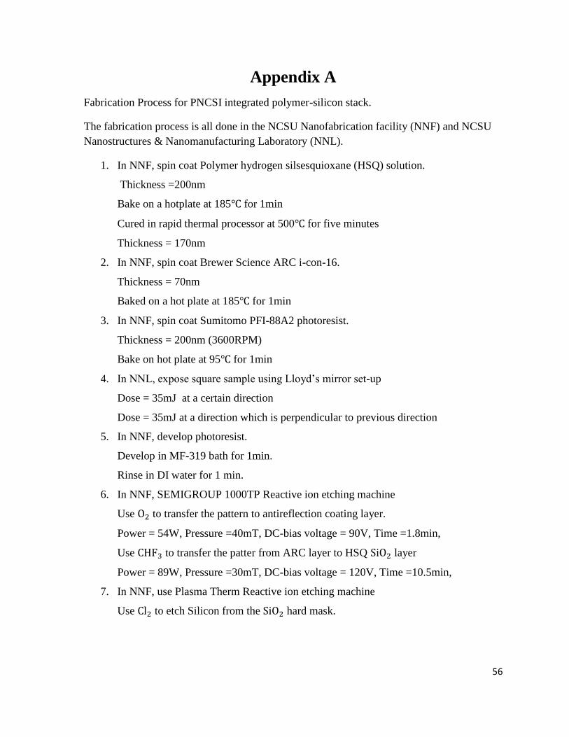
Appendix A
Fabrication Process for PNCSI integrated polymer-silicon stack.
The fabrication process is all done in the NCSU Nanofabrication facility (NNF) and NCSU
Nanostructures & Nanomanufacturing Laboratory (NNL).
1. In NNF, spin coat Polymer hydrogen silsesquioxane (HSQ) solution.
Thickness =200nm
Bake on a hotplate at 185 for 1min
Cured in rapid thermal processor at 500 for five minutes
Thickness = 170nm
2. In NNF, spin coat Brewer Science ARC i-con-16.
Thickness = 70nm
Baked on a hot plate at 185 for 1min
3. In NNF, spin coat Sumitomo PFI-88A2 photoresist.
Thickness = 200nm (3600RPM)
Bake on hot plate at 95 for 1min
4. In NNL, expose square sample using Lloyd’s mirror set-up
Dose = 35mJ at a certain direction
Dose = 35mJ at a direction which is perpendicular to previous direction
5. In NNF, develop photoresist.
Develop in MF-319 bath for 1min.
Rinse in DI water for 1 min.
6. In NNF, SEMIGROUP 1000TP Reactive ion etching machine
Use to transfer the pattern to antireflection coating layer.
Power = 54W, Pressure =40mT, DC-bias voltage = 90V, Time =1.8min,
Use to transfer the patter from ARC layer to HSQ layer
Power = 89W, Pressure =30mT, DC-bias voltage = 120V, Time =10.5min,
7. In NNF, use Plasma Therm Reactive ion etching machine
Use to etch Silicon from the hard mask.

57
8. In NNF, RCA clean to remove residue photoresist and antireflection coating
H2O : H2O2 : NH4 = 5 : 1 : 1
Temperature =
Clean time = 20min.


![PERIODIC CLASSIFICATION & PERIODIC PROPERTIES [ 1 ...youvaacademy.com/youvaadmin/image/PERIODIC TABLE BY RS.pdf · [ 2 ] PERIODIC CLASSIFICATION & PERIODIC PROPERTIES BY RAJESH SHAH](https://img.pdfslide.net/doc/110x75/604570870a43592d4f6b3e29/periodic-classification-periodic-properties-1-table-by-rspdf-2.jpg)