Embed Size (px)
Citation preview

SANDIA REPORT SAND2009-2550 Unlimited Release Printed April 2009
“Bottom-up” Meets “Top-down”: Self-Assembly to Direct Manipulation of Nanostructures on Length Scales from Atoms to Microns Brian S. Swartzentruber Prepared by Sandia National Laboratories Albuquerque, New Mexico 87185 and Livermore, California 94550
Sandia is a multiprogram laboratory operated by Sandia Corporation, a Lockheed Martin Company, for the United States Department of Energy’s National Nuclear Security Administration under Contract DE-AC04-94AL85000.
Approved for public release; further dissemination unlimited.

2
Issued by Sandia National Laboratories, operated for the United States Department of Energy by Sandia Corporation. NOTICE: This report was prepared as an account of work sponsored by an agency of the United States Government. Neither the United States Government, nor any agency thereof, nor any of their employees, nor any of their contractors, subcontractors, or their employees, make any warranty, express or implied, or assume any legal liability or responsibility for the accuracy, completeness, or usefulness of any information, apparatus, product, or process disclosed, or represent that its use would not infringe privately owned rights. Reference herein to any specific commercial product, process, or service by trade name, trademark, manufacturer, or otherwise, does not necessarily constitute or imply its endorsement, recommendation, or favoring by the United States Government, any agency thereof, or any of their contractors or subcontractors. The views and opinions expressed herein do not necessarily state or reflect those of the United States Government, any agency thereof, or any of their contractors. Printed in the United States of America. This report has been reproduced directly from the best available copy. Available to DOE and DOE contractors from U.S. Department of Energy Office of Scientific and Technical Information P.O. Box 62 Oak Ridge, TN 37831 Telephone: (865) 576-8401 Facsimile: (865) 576-5728 E-Mail: [email protected] Online ordering: http://www.osti.gov/bridge Available to the public from U.S. Department of Commerce National Technical Information Service 5285 Port Royal Rd. Springfield, VA 22161 Telephone: (800) 553-6847 Facsimile: (703) 605-6900 E-Mail: [email protected] Online order: http://www.ntis.gov/help/ordermethods.asp?loc=7-4-0#online

3
SAND2009-2550 Unlimited Release Printed April 2009
“Bottom-up” Meets “Top-down”: Self-Assembly to Direct Manipulation of Nanostructures on Length Scales from Atoms to Microns
Brian S. Swartzentruber CINT Sciences Department
Sandia National Laboratories P.O. Box 5800
Albuquerque, New Mexico 87185-MS1303
Abstract
This document is the final SAND Report for the LDRD Project 102660 – “Bottom-up” meets “top-down”: Self-assembly to direct manipulation of nanostructures on length scales from atoms to microns” – funded through the Strategic Partnerships investment area as part of the National Institute for Nano-Engineering (NINE) project.

4
ACKNOWLEDGMENTS This project was done in collaboration with Gary Kellogg (1132), Ezra Bussmann (1132), Ivan Ermanowski (1132), Norm Bartelt (8656), Franz Himpsel (University of Wisconsin-Madison), and Joanna Mirecki-Milluchick (University of Michigan). Section 2 was written by Ivan Ermanowski and Section 3 was written by Ezra Bussmann.

5
CONTENTS
1. Introduction ................................................................................................................................ 7
2. Perfectly ordered stripe arrays on B-doped Si(100) ................................................................ 11
3. One-dimensional defect-mediated adatom diffusion on the Si(111)-5×2-Au surface ............. 18
Distribution ................................................................................................................................... 25

6

7
1. Introduction This program was centered on the development and application of state-of-the-art instrumentation for the fabrication and characterization of engineered nanopatterns and nanostructures on surfaces. We combined measurements using low-energy electron microscopy (LEEM) and scanning probe microscopy (SPM) to compare direct imaging of surface features on length scales from atoms to microns. We used these capabilities to investigate processes underlying the “bottom-up” generation of surface nanostructures, i.e., the spontaneous formation of one- and two-dimensional surface features that can serve as templates for three-dimensional nanostructures. This bottom-up approach was complemented with the development of a novel nano-manipulator inside of a scanning electron microscope for “top-down” construction and characterization of unique nanostructures such as metallic and semiconducting nanorods and wires. This tool enables not only direct and precise control over the placement of individual nanostructures, but also of their position with respect to each other – an ideal unattainable by present means. The incorporation of these unique capabilities will have impact in establishing NINE programs that interact with both universities and industry. Our partner at the University of Wisconsin, Prof. Franz Himpsel, is a world-renown expert in the growth and characterization of nanowires on surfaces. We also partnered with Prof. Joanna Mirecki Millunchick at the University of Michigan. She and a graduate student studied the directed self-assembly of InAs quantum dots using focused ion beam and atomic force microscopy. The “bottom-up” portion of this program was concerned with the spontaneous formation of one- and two-dimensional surface features that could possibly serve as templates for three-dimensional structures. We studied a striking example of this phenomenon – the formation of stripe patterns on Si(001) induced by the presence of boron. Our current interest in this system is whether this type of self-assembly can be used to create stable patterns over large distances (tens of microns) and whether the patterns can be stabilized to room temperature. A fundamental understanding of the factors that control pattern uniformity (defect interactions) and periodicity (elastic interaction) is the key to achieving this goal. LEEM images demonstrating recent progress are shown in Fig. 1. The stripe patterns are confined to atomically flat regions on the surface. We created these flat areas by etching shallow pits in the surface (lithography/reactive ion etching) and sublimating Si until step flow smoothed out the pit bottoms. At a temperature of approximately 900C, one-dimensional vacancy islands nucleate within the flat region and grow across the terrace. Ordering takes place by a mechanism in which stripes larger than a critical width split into two. Future work will involve characterizing the conductive properties of the metal decorated steps, and learning how to make more highly ordered stripe structures on ultra-large terraces. To understand the stability of self-assembled structures, we need to determine the processes and energetics responsible for their formation and decay, both thermodynamics and
Fig. 1: LEEM images of self-assembled stripe patterns on heavily B-doped Si(001). (a) 870 C (b) near room temperature. The top arrow in (a) points to a dislocation (end of stripe), the bottom arrow points to a stripe that is splitting.
8
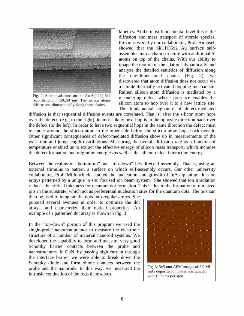
kinetics. At the most fundamental level this is the diffusion and mass transport of atomic species. Previous work by our collaborator, Prof. Himpsel, showed that the Si(111)5x2 Au surface self-assembles into a chain structure with additional Si atoms on top of the chains. With our ability to image the motion of the adatoms dynamically and analyze the detailed statistics of diffusion along the one-dimensional chains (Fig. 2), we discovered that atom diffusion does not occur via a simple thermally-activated hopping mechanism. Rather, silicon atom diffusion is mediated by a meandering defect whose presence enables the silicon atom to hop over it to a new lattice site. The fundamental signature of defect-mediated
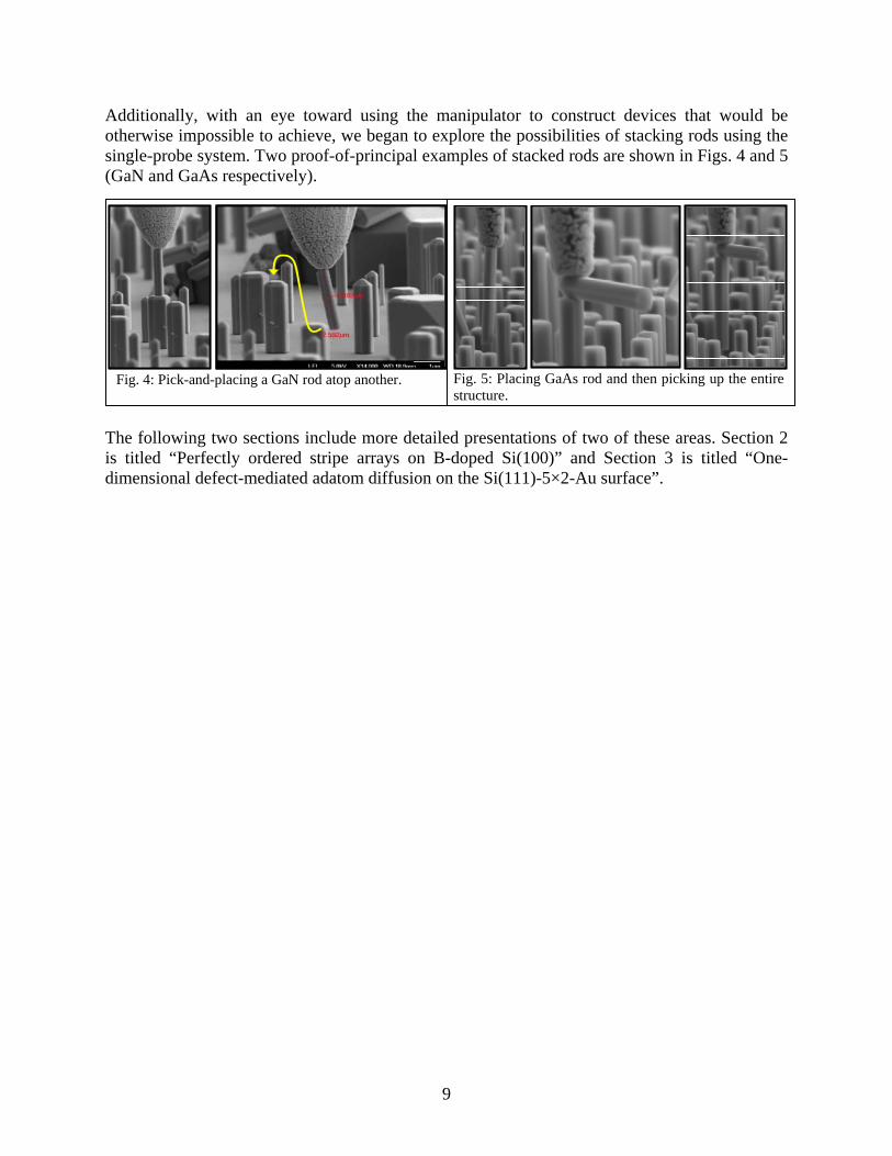
diffusion is that sequential diffusion events are correlated. That is, after the silicon atom hops over the defect, (e.g., to the right), its most likely next hop is in the opposite direction back over the defect (to the left). In order to have two sequential hops in the same direction the defect must meander around the silicon atom to the other side before the silicon atom hops back over it. Other significant consequences of defect-mediated diffusion show up in measurements of the wait-time and jump-length distributions. Measuring the overall diffusion rate as a function of temperature enabled us to extract the effective energy of silicon mass transport, which includes the defect formation and migration energies as well as the silicon-defect interaction energy. Between the realms of “bottom-up” and “top-down” lies directed assembly. That is, using an external stimulus to pattern a surface on which self-assembly occurs. Our other university collaborator, Prof. Millunchick, studied the nucleation and growth of InAs quantum dots on arrays patterned by a unique in situ focused ion beam system. She showed that ion irradiation reduces the critical thickness for quantum dot formation. This is due to the formation of nm-sized pits in the substrate, which act as preferential nucleation sites for the quantum dots. The pits can then be used to template the dots into regular arrays. She pursued several avenues in order to optimize the dot arrays, and characterize their optical properties. An example of a patterned dot array is shown in Fig. 3. In the “top-down” portion of this program we used the single-probe nanomanipulator to measure the electronic structure of a number of material nanorod systems. We developed the capability to form and measure very good Schottky barrier contacts between the probe and nanostructures. In GaN, by passing high current through the interface barrier we were able to break down the Schottky diode and form ohmic contacts between the probe and the nanorods. In this way, we measured the intrinsic conduction of the rods themselves.
Fig. 2: Silicon adatoms on the Au-Si(111) 5x2 reconstruction: (50x50 nm) The silicon atoms diffuse one-dimensionally along these chains.
Fig. 3: 5x5 mm AFM images of 2.0 ML InAs deposited on patterns irradiated with 1500 ms per spot.
9
Additionally, with an eye toward using the manipulator to construct devices that would be otherwise impossible to achieve, we began to explore the possibilities of stacking rods using the single-probe system. Two proof-of-principal examples of stacked rods are shown in Figs. 4 and 5 (GaN and GaAs respectively).
The following two sections include more detailed presentations of two of these areas. Section 2 is titled “Perfectly ordered stripe arrays on B-doped Si(100)” and Section 3 is titled “One-dimensional defect-mediated adatom diffusion on the Si(111)-5×2-Au surface”.
Fig. 4: Pick-and-placing a GaN rod atop another. Fig. 5: Placing GaAs rod and then picking up the entire structure.

10

11
2. PERFECTLY ORDERED STRIPE ARRAYS ON B-DOPED SI(100)
Self-assembled nanostructures are a fascinating and exciting area of research that has attracted both theoretical and experimental interest. The goal of many of these studies has been to identify systems of interest, understand the mechanisms that lead to self-assembly, and ultimately control the properties of self-assembled nanostructures. 2D-Stripe formation as a phenomenon has been theoretically predicted by Ng and Vanderbilt1. Other theoretical studies2 have shown that step energy minimization is not always the only, nor indeed dominant factor determining the equilibrium shape of 2D islands, and that, under certain conditions, island equilibrium shape can significantly deviate from that expected based solely on step energy considerations. Stripe formation on the technologically important Si(100)-(2x1) surface in the presence of boron doping was observed by Jones et al.3 Subsequent work on vicinal and atomically flat Si(100)4-6 has led to the understanding of the phenomenon in terms of stress energy interactions and boron-induced lowering and eventual vanishing of the A-type step (SA) energy βA. Here we present real-time low energy electron microscopy experiments aimed at studying the processes that lead to the healing of defects and, ultimately, to the formation of perfectly ordered stripe arrays on atomically flat highly boron-doped Si(100). Si samples with ~10-20
cm-3 B concentration were thoroughly rinsed with ethanol and acetone before being placed in the vacuum chamber. The native oxide was subsequently removed by a brief flash to 1250°C in UHV. Samples were heated by electron bombardment from the rear, and temperature was measured using a W-Re thermocouple positioned near the sample. A comparison with the known temperature of the (1x1)↔(7x7) transition of Si(111) was used to correct thermocouple readings. To prepare large step-free surface areas, the samples were patterned with square pits of several sizes (sides between 5 and 30 nm, approximately 90 nm deep) using reactive ion etching (Fig. 1a). Upon sublimation in ultrahigh vacuum (UHV), vacancy islands are formed on the pit bottoms and grow toward the pit walls, leaving an increasingly large (up to 10 μm) atomically flat area on the bottom (Fig. 1b-d).7 In the course of experiments, a Si doser with an electron beam-heated high-purity Si slug, was used as needed to control the net Si flux to and from the surface. The high LEEM contrast ratio between terraces separated by single atomic steps is due to the 90° degree rotation of the LEED patterns of alternating Si dimer rows.5
FIG. 1: a) PEEM image of the patterned Si sample; b)-d) LEEM sequence of vacancy island nucleation and growth at 1050°C.

12
A typical course of surface evolution is shown in Fig. 2. At 950°C the initially flat bottom surface is rich with rapidly created, annihilated, and diffusing adatoms and vacancies.8 Much like during sample preparation, vacancies begin to aggregate into elongated islands when sufficiently high vacancy supersaturation is reached due to sublimation (Fig. 2a).9 As the sample temperature is lowered from 951°C to 894°C, these islands become extremely elongated and typically grow to span the entire pit (Fig. 2b). Island formation lowers the vacancy concentration on the remaining terrace surface which, in turn, becomes rich with adatoms. Excess adatoms easily diffuse toward the pit walls where they aggregate into adatom islands. To a smaller extent, adatom islands are also
formed at the pit bottom, away from the walls, when their supersaturation is sufficient (Fig. 2b).6 Vacancy and adatom islands split longitudinally as they grow, maintaining an extreme aspect ratio (Fig. 2b) and giving the surface its striped appearance. It is noteworthy that the entire process runs contrary to typical surface island evolution where small islands disappear, and large ones grow. Because of rapid sublimation, by the time the sample temperature is stabilized at 875°C, the pit bottom is completely covered with vacancy and adatom islands (Fig. 2c). From this point, evolution proceeds more slowly, driven by a moderate rate of sublimation. Adatom islands gradually disappear, and small vacancy islands begin to appear inside the existing vacancy islands (Fig. 2d). In the absence of an external Si flux, this process continues until this subsequent layer of vacancy islands has covered most of the pit bottom, followed by the formation of a new layer of vacancy islands, and so on ad infinitum. Two types of defects are usually seen in stripe arrays following their initial formation: incompletely split stripes, and stripes that start at the pit edge, but terminate in the pit middle, rather than spanning the entire diameter (Fig. 2d). Careful observations of stripe evolution show that in both cases the cause is independent nucleation of more stripes than can ideally be accommodated in the pit. These defects heal much too slowly to yield a defect-free structure before sublimation causes subsequent layer vacancy island formation. In order to allow for experimental times sufficiently long for defect healing we compensate for sublimation by an external Si doser. Balancing sublimation exactly at every temperature and at all times would have required tedious and frequent doser calibrations, with no apparent benefit. Therefore, we adjusted the deposition rate to avoid two typically unwanted processes: vacancy and adatom island formation. The former occurs following sufficient Si loss from the observed
FIG. 2: LEEM images of stripe array evolution. The inset shows a next-layer vacancy island.

13
layer due to sublimation. The latter indicates adatom supersaturation due to a high Si deposition rate. Long experimental times allowed by Si dosing have made it possible for us to create perfectly ordered defect-free stripe arrays, observe stripe evolution mechanisms, measure steady-state properties such as stripe density, and determine the temperature interval in which stripe formation occurs.
Perfectly ordered steady-state stripe arrays, formed after relatively long equilibration times at 924°C and 965°C are shown in Fig. 3. Stripes exhibit small, fast fluctuations at high temperature, especially hear the apices, consisting of low stiffness B-steps.10 This is an important notion, since most of the surface evolution mechanisms discussed below involve this dynamic nature of the stripes. Recalling that stripes are extremely elongated vacancy islands, their dynamic appearance indicates that the surface is rich with vacancies and adatoms that are in a state of constant and very vigorous flux. Stripes have extraordinary relative dimensions: ~8 μm long, and 50 nm wide, in some cases. By their very nature, all are the exact same thickness, the Si(100) step height of ~0.14 nm. The different stripe density for the two temperatures in Fig. 3 reflects a general trend: steady-state stripe density depends on temperature, as shown in the graph in Fig. 4. Stripe density is the highest between ~880° and 920°C. The gradual density decrease toward higher temperatures smoothly connects the extreme aspect ratio of stripes, with that of elongated vacancy islands seen in Fig. 1b. The sharp stripe density decline below 880°C is of special interest, and is discussed in more detail below. Very importantly, Si deposition and sublimation was found to have no effect on steady-state stripe density. Stripes are filled in upon deposition, and grow in width due to sublimation, but their density remains unchanged (Fig. 5). For a stripe array away from a steady state (e.g. due to temperature
FIG. 3: LEEM images of perfectly ordered stripe arrays.
Stripe Density
0
2
4
6
8
10
12
14
860 880 900 920 940 960 980
Temperature [C]
Str
ipe
De
ns
ity
[ m
-1]
FIG. 4: Steady-state stripe density as function of temperature.
a b
921°C 921°C
2μm
FIG. 5: LEEM images of the same stripe array under 2 extreme conditions: (a) excess Si deposition leads to adatom growth; (b) sublimation leads to next-layer vacancy island formation. The number of stripes is unaffected.

14
change), sublimation and Si deposition can affect the speed with which a new steady state is reached. The mechanisms through which these ordered stripe arrays are formed depend on whether achieving a steady state involves an increase or a decrease in stripe density. In the former case, two distinct mechanisms were identified: longitudinal splitting, and new stripe nucleation and growth. Both of these processes can be seen in Fig. 6. When the temperature of the sample is changed in the direction of increased stripe density, the small shape fluctuations that are always present at the stripe apices (comprising of B-steps) become increasingly large and frequent. As the temperature departure from the previous steady state is increased, so are the amplitudes of these fluctuations. Occasionally, a fluctuation becomes large enough to start freely propagating along a stripe, eventually splitting it in two. New stripes nucleate in the space between existing ones and quickly grow to the full length of the pit (Fig. 6c-d). Both of these processes are essentially identical to those responsible for the initial stripe growth (Fig. 2b). This is not surprising, since both involve a transition from a smaller to a larger number of stripes. It is important to observe that overcoming a barrier is required in both cases: a minimum fluctuation size for stripe splitting, and critical vacancy supersaturation for stripe nucleation. This means that a minimum temperature departure form a steady state is needed for their onset, and that they may be limited in the capacity to approach a new steady state arbitrarily close. Fig. 7 shows two mechanisms of stripe density decrease, typically observed upon temperature increase. Stripes shrink and disappear in very much the opposite fashion to their appearance (Fig. 7a-d). The disappearance of the outermost stripes is of special interest because it proceeds very smoothly with temperature change. Stripes simply grow smaller and disappear while seemingly flowing sideways. The remaining array rearranges in a fashion that resembles an expanding accordion. For this reason, the equilibrium density values in Fig. 3 were obtained following this type of relaxation. Shrinking and disappearance of stripes in the middle of arrays was relatively infrequent compared to that of outermost stripes, and mainly occurred after a large temperature change.
FIG. 6: LEEM images of stripe density increase via longitudinal stripe splitting, and new stripe nucleation (arrows).

15
If we view stripe shrinking as a regular ripening process, it is to be expected that outermost stripes should be the first to disappear, since, due to the slightly oval shape of a typical pit, they are smaller than neighboring stripes. By similar reasoning, the disappearance of a mid-array stripe is contingent on a decrease in size due to fluctuations. If a decrease in size is too small, the resulting outflow of vacancies is likewise small, and fluctuations can (and most of the time do) restore the stripe to a stable size. When such a stripe becomes smaller than some critical size, vacancies rapidly diffuse to neighboring stripes, leading to its prompt disappearance. A second mechanism of stripe density decrease consists of the merging of
neighboring stripes. This process is the reverse of the stripe splitting shown in Fig. 6. Like stripe splitting, it involves fluctuations during which stripes come in close proximity to each other, and sometimes merge. It also occurs relatively infrequently compared to the sideways disappearance. An aspect completely new to the study of stripe formation on highly B-doped Si(100) is the disappearance of the striped structure with temperature decrease. It was found in previous studies that stripe density increases with temperature decrease, sometimes to such an extent as to be beyond LEEM resolution limits.3 We have observed a similar trend (Fig. 4), but with the important difference of a low temperature limit of ~875°C. Fig. 8 shows the evolution of a fully striped surface following the lowering of the sample temperature from 900C to 845C. Stripes that originally span the pit diameter begin to gradually recede or split laterally and take the form of elongated islands. The structure ripens in the usual fashion, with small islands getting smaller and eventually
FIG. 7: LEEM images of stripe density decrease.
FIG. 8: LEEM images of stripe vanishing.

16
disappearing. The ripening process is very slow, as seen by the 25-minute span between its onset and the last image. Furthermore, the slow, but finite ripening rate observed in the last few frames of this experiment indicates that equilibrium island shapes and sizes had not been reached. This result shows that the unusual vanishing βA is a phenomenon restricted to a temperature range between roughly 875°C and 920°C. A delicate balance is involved in observing stripe disappearance: a temperature increase of only 10°C halts the process and the remaining islands start to elongate, while a similar decrease in temperature slows the changes to an impractically low rate form an experimental point of view. Conversely, the low rate of the stripe-to-island transformation, makes it possible to “freeze” stripes of various periodicity (typically formed below 950°C) to room temperature. In summary, we have demonstrated the possibility of creating defect-free stripe (vacancy island) arrays on the atomically flat Si(100) surface with high B doping, determined a low temperature limit for the vanishing of βA, and identified stripe array evolution mechanisms. REFERENCES 1 K.-O. Ng and D. Vanderbilt, Phys. Rev. B 52, 2177 (1995). 2 A. Li, F. Liu, and M. G. Lagally, Phys. Rev. Lett. 85, 1922 (2000); J. Tersoff and R. M.
Tromp, Phys. Rev. Lett. 70, 2782 (1993). 3 D. E. Jones, J. P. Pelz, Y. Hong et al., Phys. Rev. Lett. 77, 330 (1996). 4 J. B. Hannon, N. C. Bartelt, B. S. Swartzentruber et al., Phys. Rev. Lett. 79, 4226 (1997);
J.-F. Nielsen, H.-J. Im, J. P. Pelz et al., J. Vac. Sci. Tech. A 17, 1670 (1999). 5 J. B. Hannon, B. S. Swartzentruber, G. L. Kellogg et al., Surf. Rev. Lett. 5, 1159 (1998). 6 J.-F. Nielsen, J. P. Pelz, H. Hibino et al., Appl. Phys. Lett. 79, 3857 (2001). 7 S. Tanaka, C. C. Umbach, J. M. Blakely et al., Appl. Phys. Lett. 69, 1235 (1996). 8 R. M. Tromp and M. Mankos, Phys. Rev. Lett. 81, 1050 (1998). 9 R. M. Tromp and J. B. Hannon, Surf. Rev. Lett. 42, 1565 (2002). 10 N. C. Bartelt and R. M. Tromp, Phys. Rev. B 54, 11731 (1996).

17

18
3. ONE-DIMENSIONAL DEFECT-MEDIATED ADATOM DIFFUSION ON THE SI(111)-5×2-AU SURFACE
The Si(111)-5×2-Au surface is a member of a family of metal-induced chain reconstructions of Si [1–8]. Studies of these chain reconstructions have yielded new understanding of the physics of one-dimensional (1-d) electronic states [1-8]. The 5×2-Au surface is speckled with Si adatoms, which sit on-top of the chains at a coverage of 0.25/5×2 cell. Owing to a repulsion between adatoms, the adatoms occupy a (half-filled) 5×4 lattice [8]. The 5×4 adatom superlattice is intimately linked with the electronic properties of the surface [4–6]. In segments covered by Si adatoms, the otherwise metallic chains are semiconducting [6]. An earlier qualitative STM study found that the adatoms diffuse along the chains by hops of 2a (7.68 Å) between neighboring 5×2 cells for T > 473 K [10]. Adatom hopping causes nanometer-scale fluctuations in the surface electronic properties. The individual Si adatoms have also been utilized as bits in an atomic-scale memory [9]. In this application, adatom hopping causes errors in the stored information. A direct determination of the adatom diffusion mechanism and activation barrier is essential in predicting the time-evolution of both the nanometer-scale surface structure and electronic properties. By a statistical characterization of the diffusion, we demonstrate that the Si adatoms hop along the chains by a defect-mediated mechanism similar to the vacancy-mediated diffusion observed on some metal surfaces. Diffusion of adatoms and surface-embedded atoms often occurs by mechanisms more complex than thermally activated random hopping from one site to the next. Random walks with several jump lengths [11, 12], exchange [13, 14], and vacancy-mediated diffusion [15–19] have all been observed in experiments. Vacancy-mediated surface diffusion was first identified on Cu surfaces, where it plays an essential role in alloying and the stability of surface structure [18, 19]. Vacancy-mediated diffusion is an instance of so-called hopover processes [20]. In a hopover process, an atom’s diffusive displacements are triggered by the random arrival of some jump-instigating defect, e.g., a vacancy. The defining element of hopover diffusion is that once the diffusion event occurs, the defect is on the opposite side of the atom from its initial approach. This simple feature leads to time and direction correlations in atom displacements and diffusion statistics different from those for any uncorrelated process, e.g., random walk diffusion [16]. Intuitively, hopover diffusion is impossible in a strictly 1-d system, because sequential diffusion events arising from the defect migration are always in opposite directions leading to zero net displacement. We prepare 5×2-Au surfaces by depositing 0.4 ML Au onto clean Si(111) substrates at T ~650oC [1, 2]. The sample preparation and measurements are performed in a variable-temperature STM at pressures < 10-10 Torr. The (111) samples are miscut by ~1.0o toward the [100] azimuth. On the resulting stepped surface, each terrace (10-20 nm wide) supports only one of the three possible 5×2 domain orientations — that in which the chains run parallel to the steps. Fig. 1(a) shows a STM image of a typical surface. The Si adatoms appear as bright protrusions sitting on top of the 5×2 chain structures. Surfaces prepared at 650oC have adatom coverages of 0.21± 0.03/5 × 2 cell. A coverage near 0.25 adatoms/5 × 2 cell is obtained by annealing at 900oC for 1 minute. The coverage established during the preparation remains constant in the temperature range of the diffusion measurements.

19
To measure adatom diffusion, we take sequences of STM images at a fixed rate to create a movie. Movies consist of constant-current (0.1 nA) filled-state images acquired with -1.5 V to -2.1 V dc bias (sample) [24]. The adatoms are labeled in every frame and linked between sequential frames. The displacements are measured by following each adatom from frame-to-frame. In a typical movie, less than 10% of the 30-50 adatoms in the field of view move from frame-to-frame, so the assignment of displacements is unambiguous. The finite time for STM image acquisition restricts us to observe only net displacements from one frame to the next, not the exact sequence of hops that caused the displacement. The most straightforward way to measure the adatom diffusion barrier is to measure the
ensemble mean-square displacement rate as a function of temperature. The inset in Fig. 2 shows the measured mean-square adatom displacements between sequential frames at a few temperatures. The mean-square displacement initially increases linearly with time before turning over due to adatom crowding. Fig. 2 shows the measured adatom mean-square displacement rates versus temperature from 418 K to 488 K. The Arrhenius relation yields an activation energy barrier of 1.24 ± 0.08 eV and a prefactor 1011.6±0.9 s-1. This energy represents an effective activation barrier for the temperature-dependent time evolution of the entire system. To identify the true nature of the adatom diffusion process, we must examine the diffusion statistics explicitly: the direction and time correlations, neighbor correlations, and the displacement distribution. Our observations point directly to defect-mediated hopover diffusion. The clearest indication of hopover diffusion is seen in a correlation of displacement direction. A direction correlation occurs because, as mentioned, an adatom jump over the defect places the defect on the opposite side of the adatom, leading to increased probability of the adatom hopping back-and-forth. In our experiments, we measure a directional correlation: sequential displacements in opposite directions are 1.5 times more likely than in the
FIG. 1: (a) A STM image showing a typical 5×2-Au surface (50 × 50 nm2, -1.5 V, 0.1 nA). A clean 7×7 domain (upper left) coexists with the 5×2-Au reconstruction. (b-e) Excerpts from a STM movie at 457 K illustrating a burst of displacements (11 × 7 nm2, -2.0 V, 0.1 nA, 7.1 s/frame). (b) The adatom in the circle rests for 19 frames (135 s), then moves in three consecutive frames (c-e) by -8 a, +4 a, -2 a, as indicated by arrows. It then remains at rest for 14 frames (99 s). The circle indicates the adatom position in the preceding frame.
FIG. 2: Arrhenius plot of the mean-square adatom displacement versus temperature. The effective activation barrier, 1.24 ± 0.08 eV, is extracted from the fit (solid line) to the displacements (solid circles) measured with 0.25 ± 0.03 adatoms/5×2 cell. Open circles are for lower coverages (0.14- 0.2). The broken line, activation barrier 1.15 eV and prefactor 1011 s−1, shows the temperature- dependence predicted by using our model to fit the displacement distributions. Statistical error bars in displacements are smaller than plot symbols, temperature error bars are ±5 K. (Inset) Mean-square displacements vs. time.

20
same direction. We also observe that the displacements of a given adatom do not occur randomly with a constant probability/time. Rather, they are correlated in bursts separated by longer periods of inactivity. This is a distinctive feature of hopover diffusion. That is, displacements occur in rapid succession when the defect is in the immediate vicinity, separated by periods of inactivity when the defect wanders away or is annihilated. The sequence of images shown in Fig. 1 (b-e), from a movie at 457 K, reveals this character of the diffusion process. Burst behavior is quantified by measuring the time correlation between displacements. The time correlation is c(k) = p(k)/P , where p(k) is the measured rate for two displacements to occur separated in time by k frames, regardless of intervening displacements, and P is the average frequency of displacements for the whole ensemble over the duration of the STM movie. For a random process with a constant probability/time, the correlation is c(k) = 1. We measure both the self-correlation, relating the displacement of a given adatom to its own future displacements, and a neighbor-correlation function, cn (k, r), relating the displacements of an adatom to those of all other adatoms within a radius r. Fig. 3(a) shows the self- and neighbor-correlation functions (r = 50 Å) measured from a movie (6.8s/image) at 468 K. The displacements of a given adatom are correlated over several frames (c > 1), but become uncorrelated over longer periods. By contrast, displacements within a neighborhood are uncorrelated at all times, cn(k, 50 Å) = 1. That the displacements of neighboring adatoms are uncorrelated implies that the jump-instigating defect remains localized near a given adatom, instead of wandering over the surface. Since neighboring adatoms may be separated by as few as two 5×2 cells, the defect must be restricted to only a few atomic sites to either side of the adatom. The wait-time distribution, which is related to the time correlation function, also reveals the burst-like character of the diffusion. The wait-time distribution measures the probability for two sequential displacements to occur separated by a specific time-interval. In a random process with a constant probability/time, wait times are exponentially distributed. However, the measured wait-time distributions, Fig. 3(b) and inset, are not exponential. They show upward curvature on a log plot (inset Fig. 3(b)), indicating a high probability for rapid sequential displacements, and a long tail attributed to the extended time between subsequent revisitations of the defect to the adatom. Incidentally, this burst behavior is not observed for vacancy-mediated diffusion of embedded atoms on Cu surfaces because the duration of the interaction between the atom and the fast-moving vacancy is much shorter than the image acquisition time [16, 17].
FIG. 3: Diffusion statistics for Si adatoms on the 5×2-Au surface. Experimental measurements are represented by symbols. Solid lines, with shaded error bars, are the results of our defect-mediated model. (a) Time correlations between adatom displacements. (b) Wait-time distributions. The inset shows a comparison with a random walk model (broken line), which fails for short wait times. (c) Displacement distributions. Broken lines are for a random walk.

21
The burst character of diffusion on Cu shows up only in the displacement distribution. The displacement distribution for hopover diffusion does not follow the binomial form characteristic of a random walk. Rather, there is a higher probability for long displacements owing to the increased number of jumps during a burst. The deviation from random-walk behavior in our data is clearly seen in Fig. 3(c), in which we plot the measured frame-to-frame displacement distributions at a few temperatures along with binomial distributions of the same width. We quantify the connection between the measured statistics and defect-mediated diffusion using a Monte Carlo simulation. A schematic for our model is shown in Fig. 4. An adatom and a jump-instigating defect sit on a row of sites. The defect wanders within a space of length L, including at most only a few sites near the adatom. The essence of the 1-d hopover process is described with three rates: r, the rate at which the defect hops on lattice sites away from the adatom; r1 , the rate at which the defect passes to the other side of the adatom without affecting the adatom position; and r2 , the rate at which the adatom hops over the defect causing a diffusion event. We use the respective activation barriers, E, E1, and E2 , with a common prefactor to determine the rates in the simulation. In order to model the diffusion statistics accurately at all temperatures, it is also necessary to include a defect lifetime. The defect lifetime is determined through detailed balance by including an activation barrier for defect creation, Ec, and a defect formation energy, ∆E [25]. By an extensive exploration of possible parameter values, we have found a set of best-fit values that allows our model to accurately reproduce both the displacement and time statistics, as well as the correct temperature-dependence of these statistics across the experimental temperature range. The measured distributions and results of the model are shown in Fig. 3. The signature nonexponential and nonbinomial shapes of the wait-time and displacement distributions, respectively, are well represented. The model also reproduces the expected directional correlation of displacements. In experiment we measure sequential displacements to be in opposite directions at a rate of 60 ± 6%, at 457 K, while the model yields 55%. The diffusion statistics are simulated with the parameters: E = 1.21 eV, E1 = 1.07 eV, and E2 = 1.07 eV, and a prefactor = 2 × 10¹² s−1. The choice of L = 5 sites, two sites on each side of the adatom, is arbitrary and mainly determines the prefactor. The defect lifetime is determined by a formation energy, ∆E = 0.11 eV, and a creation barrier, Ec = 1.21 eV. Uncertainties in the energies are < 50 meV. Owing to uncertainty in our temperature measurements, the results of the simulations (heavy solid lines) at the measured temperatures (428 K, 457 K, and 476 K) are displayed with shaded temperature error bars (±5 K, -5 K, and 5 K, respectively) in Figs. 3(b) and (c). The scatter of displacements in Fig. 3(c) and mean-square displacements in Fig. 2 is consistent with uncertainties of a few Kelvin. In our model, E1 or E2 may be rate-limiting and thereby set the adatom diffusion barrier. Since E1 and E2 are identical (1.07 eV), the barrier is sensitive to both. In this situation, we have been unable to find a closed-form expression for the activation barrier. We have numerically
FIG. 4: (a) Schematic for our model of 1-d defect-mediated hopover diffusion. The diffusive jumps of the adatom (large ball) are mediated by a localized defect (black ball). (b) The potential energy surface which determines the lifetime of the defect.

22
determined the model activation barrier to be 1.15 eV, which is near the sum E2 + ∆E = 1.07 eV + 0.11 eV = 1.18 eV(= E1 + ∆E). The activation barrier measured in experiments is 1.24 ± 0.08 eV (See Fig. 2). Establishing that diffusion is defect-mediated does not reveal the nature of the defect. STM images do not offer a clear candidate, which suggests that the defect may reside sub-surface or involve subtle atomic arrangements that cannot be resolved with STM. The detailed structure and arrangement of Au and Si atoms on the 5×2-Au surface, as well as the binding site of the Si adatom, is unsettled [21, 22]. Because of the relatively large unit cell, first-principles calculations are difficult and yield several structures with similar configuration energies [23]. The measurements presented here offer some clues and provide a test for the calculated adatom binding energies. The defect is localized in the neighborhood of an adatom, and its formation energy is small ( < 0.10 eV), suggesting that it may well be an integral part of the reconstruction that becomes activated to migrate around the adatom before relaxing again to its most stable configuration. REFERENCES
[1] J. N. Crain, J. L. McChesney, F. Zheng, M. C. Gallagher, P. C. Snijders, M. Bissen, C. Gundelach, S. C. Erwin, and F. J. Himpsel, Phys. Rev. B 69, 125401 (2004).
[2] I. Barke, T. K. Rügheimer, F. Zheng, and F. J. Himpsel, Appl. Surf. Sci. 254, 4 (2007). [3] I. Barke, R. Bennewitz, J. N. Crain, S. C. Erwin, A. Kirakosian, J. L. McChesney, and F.
J. Himpsel, Solid State Comm. 142, 617 (2007). [4] S. C. Erwin, Phys. Rev. Lett. 91, 206101 (2003). [5] J. L. McChesney, J. N. Crain, V. Perez-Dieste, F. Zheng, M. C. Gallagher, M. Bissen, C.
Gundelach, and F. J. Himpsel, Phys. Rev. B 70, 195430 (2004). [6] H. S. Yoon, S. J. Park, J. E. Lee, C. N. Whang, and I.-W. Lyo, Phys. Rev. Lett. 92, 096801
(2004). [7] Y. Yagi, K. Kakitani, and A. Yoshimori, Surf. Sci. 356, 47 (1996). [8] A. Kirakosian, R. Bennewitz, F. J. Himpsel, and L. W. Bruch, Phys. Rev. B 67, 205412
(2003). [9] R. Bennewitz, J. N. Crain, A. Kirakosian, J.-L. Lin, J. L. McChesney, D. Y. Petrovykh, and
F. J. Himpsel, Nanotechnology 13, 499 (2002). [10] T. Hasegawa and S. Hosoki, Phys. Rev. B 54, 10300 (1996). [11] S. C. Wang, J. D. Wrigley, and G. Ehrlich, J. Chem. Phys. 91, 5087 (1989). [12] D. C. Senft and G. Ehrlich, Phys. Rev. Lett. 74, 294 (1995). [13] G. L. Kellogg and P. J. Feibelman, Phys. Rev. Lett. 64, 3143 (1990). [14] G. L. Kellogg, Surf. Sci. Reps. 21, 1 (1990). [15] T. Flores, S. Junghans, and M. Wuttig, Surf. Sci. 371, 1 (1997). [16] R. van Gastel, E. Somfai, S. B. van Albada, W. van Saarloos, and J. W. M. Frenken, Phys.
Rev. Lett. 86, 1562 (2001). [17] M. L. Grant, B. S. Swartzentruber, N. C. Bartelt, and J. B. Hannon, Phys. Rev. Lett. 86,
4588 (2001). [18] M. L. Anderson, M. J. D’Amato, P. J. Feibelman, and B. S. Swartzentruber, Phys. Rev.
Lett. 90, 126102 (2003). [19] J. B. Hannon, C. Klünker, M. Giesen, H. Ibach, N. C. Bartelt, and J. C. Hamilton, Phys.
Rev. Lett. 79, 2506 (1997).

23
[20] R. K. P. Zia and Z. Toroczkai, J. Phys. A : Math and Gen. 31, 9667 (1998). [21] S. Riikonen and D. Sanchez-Portal, Phys. Rev. B 71, 235423 (2005). [22] H. S. Yoon, J. E. Lee, S. J. Park, I.-W. Lyo, and M.-H. Kang, Phys. Rev. B 72, 155443
(2005). [23] S. C. Erwin, private communication. [24] We have explored the influence of the STM tip on diffusion. The mean-square
displacement rate and displacement distribution are not significantly affected by the scan rate or angle relative to the rows of the reconstruction. We have also looked for correlations between adatom displacements and the passage of the tip. We find that 1-8% of displacements may occur by tip-influence. This small correlation implies that the tip may lower the adatom diffusion barrier by less than 10 meV.
[25] Our model treats a single adatom-defect pair. Adatom interactions must be considered. A repulsive interaction between adatoms nearly excludes adatom occupation of adjacent 5 × 2 sites along-chain [7, 8]. The effects of adatom crowding and repulsion are estimated by extracting the diffusion statistics of isolated adatoms with no neighbors at or within three sites in both directions along-chain. The defect-mediated characteristic shape of their displacement distribution is nearly identical to that for the ensemble, but the average frequency of displacements is < 20% greater. Rate differences of 20% correspond to small (10 meV) modifications to the diffusion activation barriers, or < 20% adjustments of the hop prefactor.

24

25
DISTRIBUTION
1 MS0123 D. Chavez, LDRD Office 1011 1 MS0899 Technical Library 9536 (electronic copy) 1 MS1303 B. S. Swartzentruber 1132


![Self-assembly of smart mesoscopic objects...Self-assembly o ers opportunities for elaborating mesos-cale structures between bottom-up and top-down fabri-cation methods [1,2]. In particular,](https://img.pdfslide.net/doc/110x75/60941cb80c1e99596a2a3a3b/self-assembly-of-smart-mesoscopic-objects-self-assembly-o-ers-opportunities.jpg)


![[ACM-ICPC] Top-down & Bottom-up](https://img.pdfslide.net/doc/110x75/555602efd8b42a8a5f8b55b0/acm-icpc-top-down-bottom-up.jpg)


![Top Down Assembly Modeling[1]](https://img.pdfslide.net/doc/110x75/577d29e21a28ab4e1ea82487/top-down-assembly-modeling1.jpg)