Embed Size (px)
Citation preview
AP3783 Document number: DS37429 Rev. 8 - 2
1 of 17 www.diodes.com
December 2017 © Diodes Incorporated
AP3783
PRIMARY SIDE REGULATED SWITCHING MODE POWER SUPPLY CONTROLLER
Description
The AP3783 is a high performance AC/DC power supply controller for
battery charger and adapter applications. The controller regulates the
output voltage and current in the primary side by piece-wise Pulse
Frequency Modulation (p-PFM) in discontinuous conduction mode
(DCM).
The AP3783 provides accurate constant voltage (CV), constant
current (CC) and outstanding dynamic performance without requiring
an opto-coupler. It also eliminates the need of loop compensation
circuitry while maintaining stability.
The AP3783 provides valley turn-on function, operating frequency
Jitter function (about 5.5% frequency change every 256μs) from light
to full load range and 3-segment drive current to improve the power
supply EMI performance. The AP3783 also has built-in fixed cable
voltage drop compensation (4%, 7% and 12% of nominal system
output voltage to meet various cables with different length and gauge)
and adjustable line voltage compensation.
The AP3783 is packaged in SOT26.
Applications
Adapters/Chargers
LED Lighting
Standby and Auxiliary Power Supplies
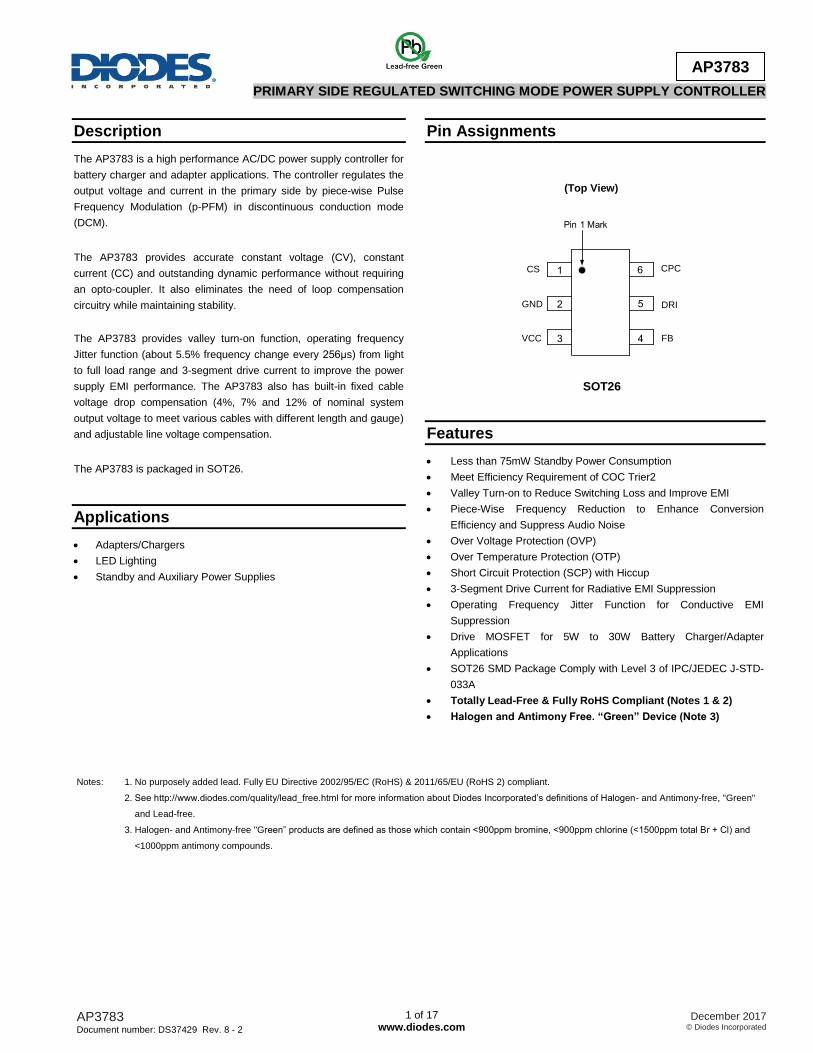
Pin Assignments
(Top View)
CS
GND
VCC
CPC
FB
DRI
1
2
3 4
5
Pin 1 Mark
6
SOT26
Features
Less than 75mW Standby Power Consumption
Meet Efficiency Requirement of COC Trier2
Valley Turn-on to Reduce Switching Loss and Improve EMI
Piece-Wise Frequency Reduction to Enhance Conversion
Efficiency and Suppress Audio Noise
Over Voltage Protection (OVP)
Over Temperature Protection (OTP)
Short Circuit Protection (SCP) with Hiccup
3-Segment Drive Current for Radiative EMI Suppression
Operating Frequency Jitter Function for Conductive EMI
Suppression
Drive MOSFET for 5W to 30W Battery Charger/Adapter
Applications
SOT26 SMD Package Comply with Level 3 of IPC/JEDEC J-STD-
033A
Totally Lead-Free & Fully RoHS Compliant (Notes 1 & 2)
Halogen and Antimony Free. “Green” Device (Note 3)
Notes: 1. No purposely added lead. Fully EU Directive 2002/95/EC (RoHS) & 2011/65/EU (RoHS 2) compliant.
2. See http://www.diodes.com/quality/lead_free.html for more information about Diodes Incorporated’s definitions of Halogen- and Antimony-free, "Green"
and Lead-free.
3. Halogen- and Antimony-free "Green” products are defined as those which contain <900ppm bromine, <900ppm chlorine (<1500ppm total Br + Cl) and
<1000ppm antimony compounds.

AP3783 Document number: DS37429 Rev. 8 - 2
2 of 17 www.diodes.com
December 2017 © Diodes Incorporated
AP3783
Typical Applications Circuit
CIN2
FR1
Da
T1D1
FB
RFB1
DRI
CPC
RCS
RFB2
CS
CVCC
U1
GND
VCC
CCPC
RST1
RST2
Q1
12V/1.5A
5V/2A
C2 R2
COUT2
DIN
R0
R1C1
DCOUT1
CY1
AP3783
RDUMMY
CIN1
Np
Ns
Na
+ +
+ +
+
LIN
Ra
1
2
3 4
5
6
Dg
Rg
Pin Descriptions
Pin Number Pin Name Function
1 CS The CS is the current sense pin of the IC. The IC will turn off the power MOSFET according to the voltage on the CS pin
2 GND The ground of the controller
3 VCC The VCC pin supplies the power for the IC. In order to get the correct operation of the IC, a capacitor with low ESR should be placed as close as possible to the VCC pin
4 FB The CV and CC regulation are realized based on the voltage sampling of this pin
5 DRI Output pin to drive external MOSFET
6 CPC A capacitor about 50nF should be connected to this pin. The voltage of CPC pin is linear to load of the system and it is used for the functions of cable voltage drop compensation and audio noise suppression

AP3783 Document number: DS37429 Rev. 8 - 2
3 of 17 www.diodes.com
December 2017 © Diodes Incorporated
AP3783
Functional Block Diagram
Regulator
&Bias
OVPOCkp
OTP
PFM
UVLO
CV_ctrl
PFM
Driver
R Q
S
R Q
S
FB
CS
VCC
DRI
GND
Constant Voltage Control
Cable compensation
Constant Current Control
0.05V
VFB_REF
1
3
5
2
6
4 COMP
Peak Current Control
LEB
Frequency Dither
VCSN Select
Dynamic
Response
Pro
Dyn
Shutdown
Pre_Shutdown
Line
Comp.
tONStONS Detector
OSC
UVUV
VLOAD
Valley
ON
VLOAD
CC_CTRL
Output short
tONS
CPC
tOSC
Detect
pulse
VLOAD UV
Detect ON
Detect ON
VLOAD
tOSC
CPC
VCS_D/L/M/H
VCS_D/L/M/H

AP3783 Document number: DS37429 Rev. 8 - 2
4 of 17 www.diodes.com
December 2017 © Diodes Incorporated
AP3783
Absolute Maximum Ratings (Note 4)
Symbol Parameter Rating Unit
VCC Supply Voltage -0.3 to 35 V
VCS, VCPC Voltage on CS, CPC Pin -0.3 to 7 V
VFB FB Input Voltage -0.4 to 10 V
ISOURCE Source Current from OUT Pin Internally Limited A
TJ Operating Junction Temperature -40 to +150 °C
TSTG Storage Temperature -65 to +150 °C
TLEAD Lead Temperature (Soldering, 10 sec) +300 °C
θJA Thermal Resistance (Junction to Ambient) 200 °C/W
ESD ESD (Human Body Model) 6000 V
ESD (Charged Device Model) 400 V
Note 4: Stresses greater than those listed under “Absolute Maximum Ratings” may cause permanent damage to the device. These are stress ratings only, and functional operation of the device at these or any other conditions beyond those indicated under “Recommended Operating Conditions” is not implied. Exposure to “Absolute Maximum Ratings” for extended periods may affect device reliability.
Electrical Characteristics (@VCC =15V, TA = +25°C, unless otherwise specified.)
Symbol Parameters Conditions Min Typ Max Unit
STARTUP AND UVLO SECTION
VTH_ST Startup Threshold – 13 15.5 18 V
VOPR(MIN) Minimal Operating Voltage – 6 6.8 7.6 V
STANDBY CURRENT SECTION
IST Startup Current VCC = VTH_ST - 1V before startup
0 0.2 0.6 μA
ICC_OPR Operating Current Static current @ no load 300 450 600
DRIVING OUTPUT SECTION
VGATE Gate Voltage – 12 13 14 V
ISOURCE_L Low Driver Source Current – 17.5 20 22.5 mA
ISOURCE_H High Driver Source Current – 100 110 120 mA
VTH High/Low Driver Source Current Threshold Voltage
– 6 6.5 7 V
RSINK Sink Resistance – 5.5 6.5 7.5 Ω

AP3783 Document number: DS37429 Rev. 8 - 2
5 of 17 www.diodes.com
December 2017 © Diodes Incorporated
AP3783
Electrical Characteristics (Cont.) (@VCC = 15V, TA = +25°C, unless otherwise specified.)
Symbol Parameters Conditions Min Typ Max Unit
OPERATING FREQUENCY SECTION
fS(MAX) The Maximum Operating Frequency IO(MAX) (Note 5) – – 60 kHz
tOFF(MAX) Maximum Off Time 691 768 845 μs
tSAMPLE_H
Sample Time
57% to 100% IO(MAX) 5.2 5.8 6.4 μs
tSAMPLE_M 34% to 57% IO(MAX) (Note 6)
4.3 4.8 5.3 μs
tSAMPLE_L 5.5% to 34% IO(MAX) (Note 6)
2.7 3 3.3 μs
tSAMPLE_D 0% to 5.5% IO(MAX) (Note 6)
1.5 1.7 1.9 μs
FREQUENCY JITTER SECTION
ΔVCS/VCS VCS Modulation 5.5% load to 100% IO(MAX) 4.5 5 5.5 %
fMOD VCS Modulation Frequency 5.5% load to 100% IO(MAX) 3.6 4 4.4 kHz
CURRENT SENSE SECTION
VCS_H Peak Current Sense Threshold Voltage 57% to 100% IO(MAX) 828 900 972 mV
VCS_M As Above 34% to 57% IO(MAX)
(Note 6) 690 750 810 mV
VCS_L As Above 5.5% to 34% IO(MAX) (Note 6)
414 450 486 mV
VCS_D As Above 0% to 5.5% IO(MAX) (Note 6)
230 250 270 mV
RLINE Built-in Line Compensation Resistor (Note 7) 245 260 275 Ω
tLEB Leading Edge Blanking VCS (Note 6) 495 550 605 ns
CONSTANT VOLTAGE SECTION
VFB Feedback Voltage Closed loop test of VOUT 3.95 4.01 4.07 V
RFB FB Pin Input Resistance VFB=4V 560 700 840 kΩ
VCABLE
/VOUT%
Cable Compensation Ratio
AP3783A 6 7 8 %
AP3783B 3 4 5 %
AP3783C 10 12 14 %
CONSTANT CURRENT SECTION
tONS/tSW Secondary Winding Conduction Duty VFB = 3.5V 0.47 0.5 0.53 –
VALLEY-ON SECTION
tVAL-ON Valid Off Time of Valley-on From the end of tONS 14.4 16 17.6 μs
DYNAMIC SECTION
VUV_H Under Voltage of FB Pin for VCS_H – 3.61 3.68 3.75 V
PROTECTION FUNCTION SECTION
VFB(OVP) Over Voltage Protection at FB Pin – 7.1 7.5 7.9 V
VCC(OVP) Over Voltage Protection at VCC Pin – 28 30 32 V
tONP(MAX) Maximum Turn-on Time – 13.5 16 25 μs
VFB(SCP) Short Circuit Protection VFB @ Hiccup 2.45 2.6 2.75 V
tSCP Maximum Time under VFB(SCP) – 115 128 141 ms
TOTP Shutdown Temperature – +144 +160 +176 °C
THYS Temperature Hysteresis – +36 +40 +44 °C
Notes: 5. The output constant-current design value, generally set to 110% to 120% of full load. 6. Guaranteed by Design.
7. Line compensation voltage on CS reference:
AUX
LINE1FB
LINE
REF_CS VRR
R438.0V
Δ

AP3783 Document number: DS37429 Rev. 8 - 2
6 of 17 www.diodes.com
December 2017 © Diodes Incorporated
AP3783
Performance Characteristics
Start-up Voltage vs. Ambient Temperature Start-up Current vs. Ambient Temperature
-40 -20 0 20 40 60 80 100 120 14013.0
13.5
14.0
14.5
15.0
15.5
16.0
16.5
17.0
Ambient Temperature (
oC)
Sta
rt-u
p V
olta
ge
(V
)
-40 -20 0 20 40 60 80 100 120 1400.0
0.2
0.4
0.6
0.8
1.0
Sta
rt-u
p C
urr
en
t (
A)
Ambient Temperature (oC)
Minimal Operating Voltage vs. Ambient Temperature Operating Current vs. Ambient Temperature
-40 -20 0 20 40 60 80 100 120 1403
4
5
6
7
8
Ambient Temperature (oC)
Min
imu
n O
pe
ratin
g V
olta
ge
(V
)
-40 -20 0 20 40 60 80 100 120 140200
250
300
350
400
450
500
Ambient Temperature (oC)
Op
era
tin
g C
urr
en
t (
A)
Sink Resistance vs. Ambient Temperature Sample Time vs. Ambient Temperature
-40 -20 0 20 40 60 80 100 120 1400
2
4
6
8
10
12
14
Ambient Temperature (oC)
Sin
k R
esis
tan
ce
(
)
-40 -20 0 20 40 60 80 100 120 1402
3
4
5
6
7
Ambient Temperature (
oC)
Sa
mp
le T
ime
(s)
AP3783 Document number: DS37429 Rev. 8 - 2
7 of 17 www.diodes.com
December 2017 © Diodes Incorporated
AP3783
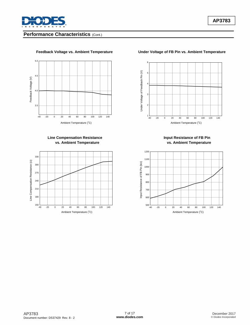
Performance Characteristics (Cont.)
Feedback Voltage vs. Ambient Temperature Under Voltage of FB Pin vs. Ambient Temperature
-40 -20 0 20 40 60 80 100 120 140
3.5
4.0
4.5
5.0
Ambient Temperature (
oC)
Fe
ed
ba
ck V
olta
ge
(V
)
-40 -20 0 20 40 60 80 100 120 1401
2
3
4
5
6
Ambient Temperature (oC)
Un
de
r V
olta
ge
of F
ee
db
ack P
in (
V)
Line Compensation Resistance Input Resistance of FB Pin
vs. Ambient Temperature vs. Ambient Temperature
-40 -20 0 20 40 60 80 100 120 140150
180
210
240
270
300
330
Ambient Temperature (oC)
Lin
e C
om
pe
nsa
tio
n R
esis
tan
ce
(
)
-40 -20 0 20 40 60 80 100 120 140500
600
700
800
900
1000
1100
1200
Ambient Temperature (oC)
Inp
ut R
esis
tan
ce
of F
B P
in (
k
)

AP3783 Document number: DS37429 Rev. 8 - 2
8 of 17 www.diodes.com
December 2017 © Diodes Incorporated
AP3783
Operation Principle Description
CIN2
FR1
Da
T1D1
FB
RFB1
DRI
CPC
RCS
RFB2
CS
CVCC
U1
GND
VCC
CCPC
RST1
RST2
Q1
12V/1.5A
5V/2A
C2 R2
COUT2
DIN
R0
R1C1
DCOUT1
CY1
AP3783
RDUMMY
CIN1
Np
Ns
Na
+ +
+ +
+
LIN
Ra
1
2
3 4
5
6
Dg
Rg
Figure 1. Typical Application Circuit of AP3783
Figure 1 is the typical application circuit of AP3783, which is a conventional Flyback converter with a 3-winding transformer---primary winding (NP),
secondary winding (NS) and auxiliary winding (NAUX). The auxiliary winding is used for providing VCC supply voltage for IC and sensing the output
voltage feedback signal to FB pin.
Figure 2 shows the typical waveforms which demonstrate the basic operating principle of AP3783 application. And the parameters are defined as
following.
IP---The primary side current
IS ---The secondary side current
IPK---Peak value of primary side current
IPKS---Peak value of secondary side current
VSEC---The transient voltage at secondary winding
VS---The stable voltage at secondary winding when rectification diode is in conducting status, which equals the sum of output voltage VOUT and
the forward voltage drop of diode
VAUX---The transient voltage at auxiliary winding
VA--- The stable voltage at auxiliary winding when rectification diode is in conducting status, which equals the sum of voltage VCC and the forward
voltage drop of auxiliary diode
tSW ---The period of switching frequency
tONP ---The conduction time when primary side switch is “ON”
tONS ---The conduction time when secondary side diode is “ON”
tOFF ---The dead time when neither primary side switch nor secondary side diode is “ON”
tOFFS --- The time when secondary side diode is “OFF”

AP3783 Document number: DS37429 Rev. 8 - 2
9 of 17 www.diodes.com
December 2017 © Diodes Incorporated
AP3783
Operation Principle Description (Cont.)
Figure 2. The Operation Waveform of Flyback PSR System
For primary-side regulation, the primary current ip(t) is sensed by a current sense resistor RCS (as shown in Figure 1).The current rises up
linearly at a rate of:
M
IN
L
)t(V
dt
)t(dip (1)
As illustrated in Figure 2, when the current ip(t) rises up to IPK, the switch Q1 turns off. The constant peak current is given by:
CS
CSPK
R
VI (2)
The energy stored in the magnetizing inductance LM each cycle is therefore:
2
PKM IL2
1Eg (3)
So the power transferring from the input to the output is given by:
SW
2
PKM fIL2
1P (4)
Where, the fSW is the switching frequency. When the peak current IPK is constant, the output power depends on the switching frequency fSW.
Constant Voltage Operation
As to constant-voltage (CV) operation mode, the AP3783 detects the auxiliary winding voltage at FB pin to regulate the output voltage. The
auxiliary winding voltage is coupled with secondary side winding voltage, so the auxiliary winding voltage at D1 conduction time is:
DO
S
AUXAUX VV
N
NV (5)
Where the VD is the diode forward voltage drop.
t ONP t ONS
I PK
I PKS
V S
I P
I S t OFFS
t OFF
V SEC
V A V AUX
t SW

AP3783 Document number: DS37429 Rev. 8 - 2
10 of 17 www.diodes.com
December 2017 © Diodes Incorporated
AP3783
Operation Principle Description (Cont.)
0V
See Equation 5
tONS
tSAMPLE
Figure 3. Auxiliary Voltage Waveform The voltage detection point is at a constant delay time of the D1 on-time. The constant delay time is changed with the different primary peak
current. The CV loop control function of AP3783 then generates a D1 off-time to regulate the output voltage.
Constant Current Operation
The AP3783 can work in constant-current (CC) mode. Figure 2 shows the secondary current waveforms.
In CC operation mode, the CC control loop of AP3783 will keep a fixed proportion between D1 on-time tONS and D1 off-time tOFFS. The fixed
proportion is
4
4
t
t
OFFS
ONS (6)
The relationship between the output current and secondary peak current IPKS is given by:
OFFSONS
ONSPKSOUT
tt
tI
2
1I
(7)
As to tight coupled primary and secondary winding, the secondary peak current is
PK
S
PPKS I
N
NI (8)
Thus the output constant-current is given by:
PK
S
P
OFFSONS
ONSPK
S
POUT I
N
N
8
2
tt
tI
N
N
2
1I
(9)
Therefore, AP3783 can realize CC mode operation by constant primary peak current and fixed diode conduction duty cycle. Multiple Segment Constant Peak Current
As to the original PFM PSR system, the switching frequency decreases with output current decreasing, which will encounter audible noise issue
since switching frequency decreases to audio frequency range, about less than 20kHz.
In order to avoid audible noise issue, AP3783 uses 4-segment constant primary peak current control method. At constant voltage mode, the
current sense threshold voltage is multiple segments with different loading, as shown in Figure 4, which are VCS_H for high load, VCS_M for
medium load, VCS_L for light load and VCS_D for ultra light load. At constant current mode, the peak current is still VCS_H.

AP3783 Document number: DS37429 Rev. 8 - 2
11 of 17 www.diodes.com
December 2017 © Diodes Incorporated
AP3783
Operation Principle Description (Cont.)
fSW
Full load IO
38.9KHz
34% 57%5.5%
IO
VCS_REF
12KHz
IO(MAX)
24.5KHz
68KHz
31.2KHz
45KHz50KHz55KHz
VCS_L
VCS_H
VCS_M
VCS_D
High Load
Medium
Load
Light Load
Ultra Light
Load
Figure 4. Multiple Segment Peak Current at CV Mode It can be seen from Figure 4, with multiple segment peak current control, AP3783 power system can achieve good audible noise performance.
3-Segment Drive Current for Radiative EMI Suppression When the power switch is turned on, a turn-on spike will occur, that worsens the radiative EMI. It is an effective way to decrease drive current
before gate voltage gets to miller platform. The AP3783 uses 3-segment drive current for radiative EMI suppression, as shown in Figure 5.
When gate voltage gets to 6V, the AP3783 drive current switches from low current (typical: 20mA) to high current (typical: 110mA). When the
gate voltage gets to 10V, the drive current will decrease gradually to 0mA until the gate voltage goes up to the clamp voltage (13V).
Gate voltage
Drive current
t
10V
6.5V
High drive current=110mA
Low drive current=20mA
13V
Miller Platform
Figure 5. Drive Current and Gate Voltage

AP3783 Document number: DS37429 Rev. 8 - 2
12 of 17 www.diodes.com
December 2017 © Diodes Incorporated
AP3783
Operation Principle Description (Cont.) Leading Edge Blanking (LEB) Time
When the power switch is turned on, a turn-on spike will occur on the sense-resistor. To avoid false turn off switch, a leading-edge blanking is
built in. During this blanking time, the current sense comparator is disabled and the external power switch cannot be turned off. Furthermore,
due to multiple segment peak current design, the required maximum on time tONP changes with different load conditions. Therefore the LEB
time parameter also changes with different load conditions.
Adjustable Line Compensation and Fixed Cable Compensation
The AP3783 power system can adjust line compensation by changing the upper resistor at FB pin. The line compensation capability is
increased by decreasing the resistance of the upper FB resistor.
Cable compensation is fixed in AP3783.
Valley Turn-on
When the off time (tOFF) is lower than 16s, AP3783 power system can work with valley turn-on. It can reduce MOSFET switching on power
losses which is resulted from the equivalent output capacitance. At the same time, because of valley turn-on the switching frequency has the
random jitter feature, which will be benefited for conductive EMI performance. And valley turn-on can also reduce the power switch turn-on
spike current and then result in the better radiative EMI performance.
Frequency Jitter
Even though the valley turn on function can lead the random frequency jitter feature, an active frequency jitter function is added to AP3783 to
ensure the frequency jitter performance in the whole loading condition. By adjusting the VCS_REF with deviation of 5.0% every 256μs cycle, the
active frequency jitter can be realized.
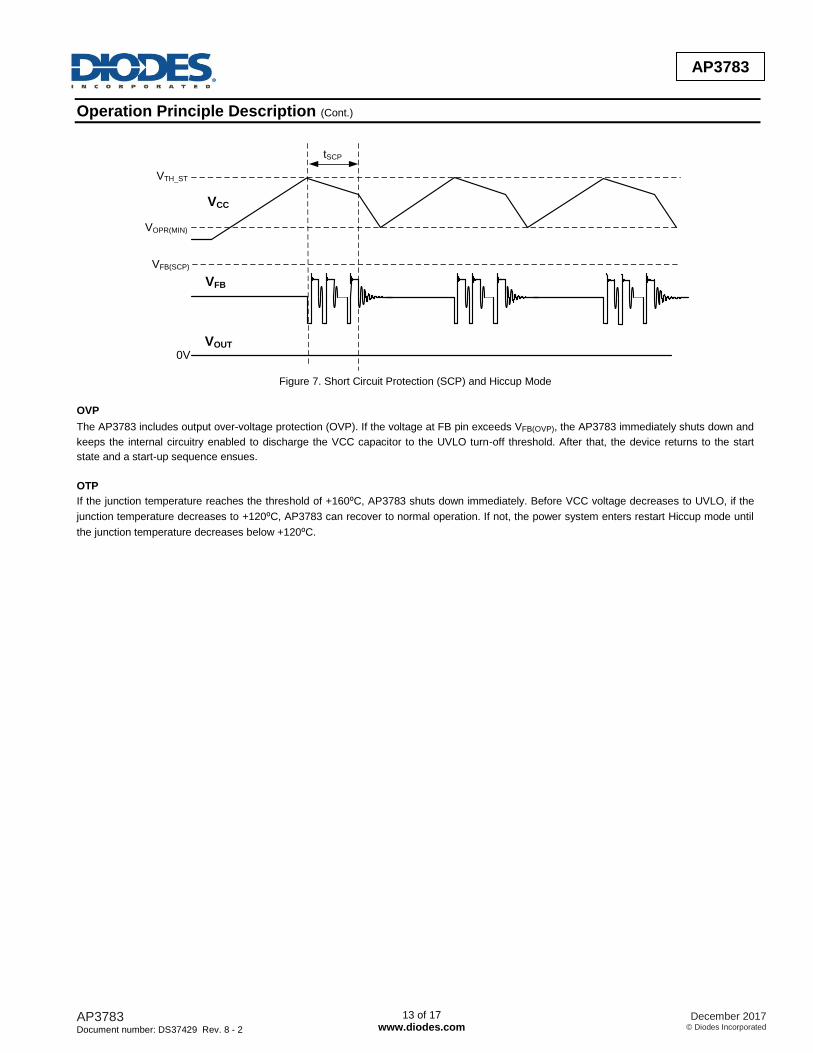
Short Circuit Protection (SCP)
Short Circuit Protection (SCP) detection principle is similar to the normal output voltage feedback detection by sensing FB pin voltage. When
the detected FB pin voltage is below VFB(SCP) for a duration of about 128ms, the SCP is triggered. Then the AP3783 enters hiccup mode that
the IC immediately shuts down and then restarts, so that the VCC voltage changes between VTH_ST and UVLO threshold until VFB(SCP) condition
is removed.
As to the normal system startup, the time duration of FB pin voltage below VFB(SCP) should be less than 18ms to avoid entering SCP mode. But
for the output short condition or the output voltage below a certain level, the SCP mode will be triggered.
Figure 6 is the AP3783 normal start-up waveform that the voltage of FB pin is above VFB(SCP) during tSCP after VCC gets to the VTH_ST, which
doesn’t enter the SCP mode. As shown in Figure 7, VOUT is short and the voltage of FB pin is lower than VFB(SCP) during tSCP, the AP3783
triggers the SCP and enters the hiccup mode.
VTH_ST
VFB(SCP)
tSCP
VCC
VFB
VOUT
VOUT(SCP)
5V
Figure 6. Normal Start-up
AP3783 Document number: DS37429 Rev. 8 - 2
13 of 17 www.diodes.com
December 2017 © Diodes Incorporated
AP3783
Operation Principle Description (Cont.)
VTH_ST
VOPR(MIN)
VFB(SCP)
tSCP
VCC
VFB
VOUT
0V
Figure 7. Short Circuit Protection (SCP) and Hiccup Mode
OVP
The AP3783 includes output over-voltage protection (OVP). If the voltage at FB pin exceeds VFB(OVP), the AP3783 immediately shuts down and
keeps the internal circuitry enabled to discharge the VCC capacitor to the UVLO turn-off threshold. After that, the device returns to the start
state and a start-up sequence ensues.
OTP
If the junction temperature reaches the threshold of +160⁰C, AP3783 shuts down immediately. Before VCC voltage decreases to UVLO, if the
junction temperature decreases to +120⁰C, AP3783 can recover to normal operation. If not, the power system enters restart Hiccup mode until
the junction temperature decreases below +120⁰C.

AP3783 Document number: DS37429 Rev. 8 - 2
14 of 17 www.diodes.com
December 2017 © Diodes Incorporated
AP3783
Ordering Information
AP3783 X XX XX- XX
PackingPackage
TR : Tape & ReelK6 : SOT26 G1 : Green
Product Name RoHS/GreenCable Compensation
Voltage
A: 7%
B: 4%
C: 12%
Package Temperature
Range
Cable Compensation
Voltage Part Number Marking ID Packing
SOT26 -40 to +85C
7% AP3783AK6TR-G1 GBZ 3000/Tape & Reel
4% AP3783BK6TR-G1 GNZ 3000/Tape & Reel
12% AP3783CK6TR-G1 GPZ 3000/Tape & Reel
Marking Information
(Top View)
: Logo XXX: Marking ID (See Ordering Information)
XXX

AP3783 Document number: DS37429 Rev. 8 - 2
15 of 17 www.diodes.com
December 2017 © Diodes Incorporated
AP3783
Package Outline Dimensions (All dimensions in mm(inch).)
(1) Package Type: SOT26
2.820(0.111)
3.100(0.122)
2.6
50
(0.1
04
)
3.0
00
(0.1
18
)
1.5
00
(0.0
59
)
1.7
00
(0.0
67
)
0.950(0.037)TYP
1.800(0.071)
2.000(0.079)
0.300(0.012)
0.500(0.020)
0.700(0.028)REF
0.100(0.004)
0.200(0.008)
0°
8°
0.200(0.008)
0.300(0.012)
0.600(0.024)
0.000(0.000)
0.150(0.006)
0.900(0.035)
1.300(0.051)
1.450(0.057)
MAX
1 2 3
456
Pin 1 Mark

AP3783 Document number: DS37429 Rev. 8 - 2
16 of 17 www.diodes.com
December 2017 © Diodes Incorporated
AP3783
Suggested Pad Layout
(1) Package Type: SOT26
E E
G Z
Y
X
Dimensions Z
(mm)/(inch) G
(mm)/(inch) X
(mm)/(inch) Y
(mm)/(inch) E
(mm)/(inch)
Value 3.600/0.142 1.600/0.063 0.700/0.028 1.000/0.039 0.950/0.037
AP3783 Document number: DS37429 Rev. 8 - 2
17 of 17 www.diodes.com
December 2017 © Diodes Incorporated
AP3783
IMPORTANT NOTICE DIODES INCORPORATED MAKES NO WARRANTY OF ANY KIND, EXPRESS OR IMPLIED, WITH REGARDS TO THIS DOCUMENT, INCLUDING, BUT NOT LIMITED TO, THE IMPLIED WARRANTIES OF MERCHANTABILITY AND FITNESS FOR A PARTICULAR PURPOSE (AND THEIR EQUIVALENTS UNDER THE LAWS OF ANY JURISDICTION). Diodes Incorporated and its subsidiaries reserve the right to make modifications, enhancements, improvements, corrections or other changes without further notice to this document and any product described herein. Diodes Incorporated does not assume any liability arising out of the application or use of this document or any product described herein; neither does Diodes Incorporated convey any license under its patent or trademark rights, nor the rights of others. Any Customer or user of this document or products described herein in such applications shall assume all risks of such use and will agree to hold Diodes Incorporated and all the companies whose products are represented on Diodes Incorporated website, harmless against all damages. Diodes Incorporated does not warrant or accept any liability whatsoever in respect of any products purchased through unauthorized sales channel. Should Customers purchase or use Diodes Incorporated products for any unintended or unauthorized application, Customers shall indemnify and hold Diodes Incorporated and its representatives harmless against all claims, damages, expenses, and attorney fees arising out of, directly or indirectly, any claim of personal injury or death associated with such unintended or unauthorized application. Products described herein may be covered by one or more United States, international or foreign patents pending. Product names and markings noted herein may also be covered by one or more United States, international or foreign trademarks. This document is written in English but may be translated into multiple languages for reference. Only the English version of this document is the final and determinative format released by Diodes Incorporated.
LIFE SUPPORT Diodes Incorporated products are specifically not authorized for use as critical components in life support devices or systems without the express written approval of the Chief Executive Officer of Diodes Incorporated. As used herein: A. Life support devices or systems are devices or systems which: 1. are intended to implant into the body, or
2. support or sustain life and whose failure to perform when properly used in accordance with instructions for use provided in the labeling can be reasonably expected to result in significant injury to the user.
B. A critical component is any component in a life support device or system whose failure to perform can be reasonably expected to cause the failure of the life support device or to affect its safety or effectiveness. Customers represent that they have all necessary expertise in the safety and regulatory ramifications of their life support devices or systems, and acknowledge and agree that they are solely responsible for all legal, regulatory and safety-related requirements concerning their products and any use of Diodes Incorporated products in such safety-critical, life support devices or systems, notwithstanding any devices- or systems-related information or support that may be provided by Diodes Incorporated. Further, Customers must fully indemnify Diodes Incorporated and its representatives against any damages arising out of the use of Diodes Incorporated products in such safety-critical, life support devices or systems. Copyright © 2017, Diodes Incorporated www.diodes.com