Embed Size (px)
Citation preview

AP7343 Document number: DS37952 Rev. 3 - 2
1 of 18 www.diodes.com
June 2016 © Diodes Incorporated
AP7343
300mA HIGH PSRR LOW NOISE LDO WITH ENABLE
Description
The AP7343 is a low dropout regulator with high output voltage
accuracy, low RDS(ON), high PSRR, low output noise and low
quiescent current. This regulator is based on a CMOS process.
The AP7343 includes a voltage reference, error amplifier, current limit
circuit and an enable input to turn it on and off. With the integrated
resistor network fixed output voltage versions can be delivered.
With its low power consumption and line and load transient response,
the AP7343 is well suited for low power handheld communication
equipment.
The AP7343 is packaged in X2-DFN1010-4 (Type B) and SOT25
packages, allows for smallest footprint and dense PCB layout.
Features
Low VIN and Wide VIN Range: 1.7V to 5.25V
Guarantee Output Current: 300mA
VOUT Accuracy ±1%
Ripple Rejection 75dB at 1kHz
Low Output Noise, 60µVrms from 10Hz to 100kHz
Quiescent Current as Low as 35µA
VOUT Fixed 0.9V to 3.6V
Totally Lead-Free & Fully RoHS Compliant (Notes 1 & 2)
Halogen and Antimony Free. “Green” Device (Note 3)
Pin Assignments
PIN1 – VOUT, PIN2 – GND, PIN3 – EN, PIN4 – VIN
(Top View)
5
3
2
1
4 NC
VOUTVIN
GND
EN
SOT25
Applications
Smart Phone/Tablet
RF Supply
Cameras
Portable Video
Portable Media Player
Wireless Adapter
Wireless Communication
Notes: 1. No purposely added lead. Fully EU Directive 2002/95/EC (RoHS) & 2011/65/EU (RoHS 2) compliant.
2. See http://www.diodes.com/quality/lead_free.html for more information about Diodes Incorporated’s definitions of Halogen- and Antimony-free,"Green"
and Lead-free.
3. Halogen- and Antimony-free "Green” products are defined as those which contain <900ppm bromine, <900ppm chlorine (<1500ppm total Br + Cl) and
<1000ppm antimony compounds.
Typical Applications Circuit
AP7343
VIN
EN GND
VOUT
VIN VOUT
CIN
1μF
COUT
1μF
EP

AP7343 Document number: DS37952 Rev. 3 - 2
2 of 18 www.diodes.com
June 2016 © Diodes Incorporated
AP7343
Pin Descriptions
Pin Number
Pin Name Function X2-DFN1010-4
(Type B) SOT25
1 5 VOUT Power Output Pin
2 2 GND Ground
3 3 EN
Enable Pin
This pin should be driven either high or low and must not be floating. Driving this pin high enables the regulator, while pulling it low puts the regulator into shutdown mode
4 1 VIN Power Input Pin
- 4 NC No connection
EP - Exposed Pad In PCB layout, prefer to use large copper area to cover this pad for better thermal dissipation, then connect this area to GND or leave it open. However, do not use it as GND electrode function alone
Functional Block Diagram
GND
VOUTVIN
EN
Current Limit VREF Thermal
Shutdown
GND
VOUTVIN
EN
Current Limit VREF Thermal
Shutdown
AP7343 (With Discharge) AP7343 (Without Discharge)
Absolute Maximum Ratings (Note 4) (@TA = +25°C, unless otherwise specified.)
Symbol Parameter Ratings Unit
ESD HBM Human Body Mode ESD Protection > 2 KV
ESD MM Machine Mode ESD Protection > 200 V
VIN Input Voltage 6.0 V
VEN Input Voltage for EN Pin 6.0 V
VOUT Output Voltage -0.3 to VIN + 0.3 V
IOUT Output Current 400 mA
PD Power Dissipation 400 mW
TA Operating Ambient Temperature -40 to +85 °C
TSTG Storage Temperature -55 to +125 °C
Note: 4. a). Stresses beyond those listed under Absolute Maximum Ratings may cause permanent damage to the device. These are stress ratings only and
functional operation of the device at these conditions is not implied. Exposure to absolute-maximum-rated conditions for extended period may affect device reliability.
b). Ratings apply to ambient temperature at +25°C. The JEDEC High-K board design used to derive this data was a 2 inch x 2 inch multilayer board with 1oz. internal power and ground planes and 2oz. copper traces on the top and bottom of the board.
Recommended Operating Conditions (@TA = +25°C, unless otherwise specified.)
Symbol Parameter Min Max Unit
VIN Input Voltage 1.7 5.25 V
IOUT Output Current 0 300 mA
TA Operating Ambient Temperature -40 +85 °C

AP7343 Document number: DS37952 Rev. 3 - 2
3 of 18 www.diodes.com
June 2016 © Diodes Incorporated
AP7343
Electrical Characteristics (@TA = +25°C, VEN = VOUT +1.0V, CIN = COUT = 1.0µF, IOUT = 1.0mA, unless otherwise specified.)
Parameter Condition Min Typ Max Units
Input Voltage TA = -40°C to +85°C 1.7 - 5.25 V
Output Voltage Accuracy (Note 11)
VOUT(T) ≥ 2.0V, VIN = VOUT(T)+1V TA = +25°C VOUT(T)*
0.99 VOUT(T)
VOUT(T)*
1.01 V
VOUT(T) < 2.0V, VIN = VOUT(T)+1V TA = +25°C VOUT(T)-
20mV VOUT(T)
VOUT(T)+
20mV
Line Regulation (dVOUT/dVIN/VOUT) VIN = (VOUT – Nom +1.0V) to 5.25V, IOUT = 1.0mA - 0.02 0.1 %/V
Load Regulation VIN = VOUT - Nom +1.0V, IOUT = 1mA to 300mA - 15 30 mV
Quiescent Current (Note 6) IOUT = 0mA - 35 60 µA
ISTANDBY VEN = 0V (Disabled) - 0.01 1.0 µA
Output Current - 300 - - mA
Fold-back Short Current (Note 7) VOUT Short to Ground - 55 - mA
PSRR (Note 8) VIN = (VOUT+1V) VDC + 0.2Vp-pAC,
VOUT ≥ 1.8V, IOUT = 30mA f = 1kHz - 75 - dB
Output Noise Voltage
(Note 8) (Note 9) BW = 10Hz to 100kHz, IOUT = 30mA - 60 - µVrms
Dropout Voltage (Note 5)
IOUT = 300mA
(X2-DFN1010-4 (Type B))
VOUT = 0.9V - 0.51 0.80
V
1.0V < VOUT 1.2V - 0.46 0.70
1.2V < VOUT 1.4V - 0.39 0.58
1.4V < VOUT 1.7V - 0.35 0.44
1.7V < VOUT 2.1V - 0.30 0.39
2.1V < VOUT 2.5V - 0.26 0.34
2.5V < VOUT 3.0V - 0.25 0.30
3.0V < VOUT 3.6V - 0.22 0.29
IOUT = 300mA (SOT25)
VOUT = 0.9V - 0.51 0.82
V
1.0V < VOUT 1.2V - 0.46 0.72
1.2V < VOUT 1.4V - 0.39 0.60
1.4V < VOUT 1.7V - 0.35 0.46
1.7V < VOUT 2.1V - 0.30 0.41
2.1V < VOUT 2.5V - 0.26 0.36
2.5V < VOUT 3.0V - 0.25 0.32
3.0V < VOUT 3.6V - 0.22 0.31
Output Voltage Temperature Coefficient
IOUT = 30mA, TA = -40°C to +85°C - ±30 - ppm/°C
Thermal Shutdown Threshold (TSHDN)
- - +150 - °C
Thermal Shutdown Hysteresis (THYS) - - +20 - °C
EN Input Low Voltage - 0 - 0.5 V
EN Input High Voltage - 1.3 - 5.25 V
EN Input Leakage VEN = 0, VIN = 5.0V or VEN = 5.0V, VIN = 0V -1.0 - +1.0 µA
On Resistance of N-Channel for Auto-Discharge (Note 10)
VIN = 4.0V, VEN = 0V (Disabled) - 30 - Ω
Thermal Resistance Junction to
Ambient (JA)
X2-DFN1010-4 (Type B) - 237 -
°C/W SOT25 - 179 -
Thermal Resistance Junction to Case
(JC)
X2-DFN1010-4 (Type B) - 96 -
SOT25 - 52 -
Notes: 5. Dropout voltage is the voltage difference between the input and the output at which the output voltage drops 2% below its nominal value. 6. Quiescent current is defined here is the difference in current between the input and the output.
7. Short circuit current is measured with VOUT pulled to GND.
8. This specification is guaranteed by design. 9. To make sure lowest environment noise minimizes the influence on noise measurement. 10. AP7343 has 2 options for output, built-in discharge and non-discharge. 11. Potential multiple grades based on following output voltage accuracy.

AP7343 Document number: DS37952 Rev. 3 - 2
4 of 18 www.diodes.com
June 2016 © Diodes Incorporated
AP7343
Typical Characteristics
0.0
0.5
1.0
1.5
2.0
0 100 200 300 400 500 600
Ou
tpu
t V
olta
ge
V O
UT
(V)
Output Current I OUT (mA)
Output Voltage vs Output CurrentVOUT=1.8V
Vin=2.8V
Vin=4.2V
Vin=5V
Vin=5.25V
0.0
0.5
1.0
1.5
2.0
2.5
3.0
3.5
0 100 200 300 400 500 600
Ou
tpu
t V
olta
ge
V O
UT
(V)
Output Current I OUT (mA)
Output Voltage vs Output CurrentVOUT=2.8V
Vin=3.8V
Vin=5V
Vin=5.25V
0.0
0.5
1.0
1.5
2.0
2.5
3.0
3.5
0 100 200 300 400 500 600
Ou
tpu
t V
olta
ge
V O
UT
(V)
Output Current I OUT (mA)
Output Voltage vs Output CurrentVOUT=3.3V
Vin=4.3V
Vin=5V
Vin=5.25V
0.0
0.5
1.0
1.5
2.0
0 1 2 3 4 5
Ou
tpu
t V
olta
ge
V O
UT
(V
)
Input Voltage V IN (V)
Output Voltage vs. Input VoltageVOUT=1.8V
1mA
30mA
50mA
0.0
0.5
1.0
1.5
2.0
2.5
3.0
0 1 2 3 4 5
Ou
tpu
t V
olta
ge
V O
UT
(V
)
Input Voltage V IN (V)
Output Voltage vs. Input VoltageVOUT=2.8V
1mA
30mA
50mA
0.0
0.5
1.0
1.5
2.0
2.5
3.0
3.5
0 1 2 3 4 5
Ou
tpu
t V
olta
ge
V O
UT
(V
)
Input Voltage V IN (V)
Output Voltage vs. Input VoltageVOUT=3.3V
1mA
30mA
50mA

AP7343 Document number: DS37952 Rev. 3 - 2
5 of 18 www.diodes.com
June 2016 © Diodes Incorporated
AP7343
Typical Characteristics (Cont.)
0
5
10
15
20
25
30
35
40
0 1 2 3 4 5
Su
pp
ly C
urr
en
t I
SS
(μ
A)
Input Voltage V IN (V)
Supply Current vs. Input VoltageVOUT=1.8V
0
5
10
15
20
25
30
35
40
0 1 2 3 4 5
Su
pp
ly C
urr
en
t I
SS
(μ
A)
Input Voltage V IN (V)
Supply Current vs. Input VoltageVOUT=2.8V
0
5
10
15
20
25
30
35
40
0 1 2 3 4 5
Su
pp
ly C
urr
en
t I
SS
(μ
A)
Input Voltage V IN (V)
Supply Current vs. Input VoltageVOUT=3.3V
1.76
1.77
1.78
1.79
1.80
1.81
1.82
1.83
1.84
-50 -25 0 25 50 75 100
V O
UT
(V
)
Temperature (℃)
Output Voltage Voltage vs TemperatureVOUT=1.8V
2.760
2.770
2.780
2.790
2.800
2.810
2.820
2.830
2.840
-50 -25 0 25 50 75 100
V O
UT
(V
)
Temperature (℃)
Output Voltage Voltage vs TemperatureVOUT=2.8V
3.260
3.270
3.280
3.290
3.300
3.310
3.320
3.330
3.340
-50 -25 0 25 50 75 100
V O
UT
(V
)
Temperature (℃)
Output Voltage Voltage vs TemperatureVOUT=3.3V
Output Voltage vs. Temperature
Output Voltage vs. Temperature Output Voltage vs. Temperature
AP7343 Document number: DS37952 Rev. 3 - 2
6 of 18 www.diodes.com
June 2016 © Diodes Incorporated
AP7343
Typical Characteristics (Cont.)
0
50
100
150
200
250
300
350
400
0 50 100 150 200 250 300
Dro
po
ut V
olta
ge
V D
IF (m
V)
Output Current I OUT (mA)
Dropout Voltage vs. Output CurrentVOUT=1.8V
25C
-40C
85C
0
50
100
150
200
250
300
0 50 100 150 200 250 300
Dro
po
ut V
olta
ge
V D
IF (m
V)
Output Current I OUT (mA)
Dropout Voltage vs. Output CurrentVOUT=2.8V
25C
-40C
85C
0
50
100
150
200
250
300
0 50 100 150 200 250 300
Dro
po
ut V
olta
ge
V D
IF (m
V)
Output Current I OUT (mA)
Dropout Voltage vs. Output CurrentVOUT=3.3V
25C
-40C
85C
0
20
40
60
80
100
120
100 1000 10000 100000 1000000
Rip
ple
Re
jectio
n R
R (
dB
)
Frequency f (Hz)
Ripple Rejection vs. FrequencyVOUT=1.8V
Iout=1mA
Iout=30mA
Iout=150mA
0
20
40
60
80
100
120
100 1000 10000 100000 1000000
Rip
ple
Re
jectio
n R
R (
dB
)
Frequency f (Hz)
Ripple Rejection vs. FrequencyVOUT=2.8V
Iout=1mA
Iout=30mA
Iout=150mA
0
20
40
60
80
100
120
100 1000 10000 100000 1000000
Rip
ple
Reje
ctio
n R
R (
dB
)
Frequency f (Hz)
Ripple Rejection vs. FrequencyVOUT=3.3V
Iout=1mA
Iout=30mA
Iout=150mA
25°C -40°C 85°C
25°C -40°C 85°C
25°C -40°C 85°C
AP7343 Document number: DS37952 Rev. 3 - 2
7 of 18 www.diodes.com
June 2016 © Diodes Incorporated
AP7343
Typical Characteristics (Cont.)
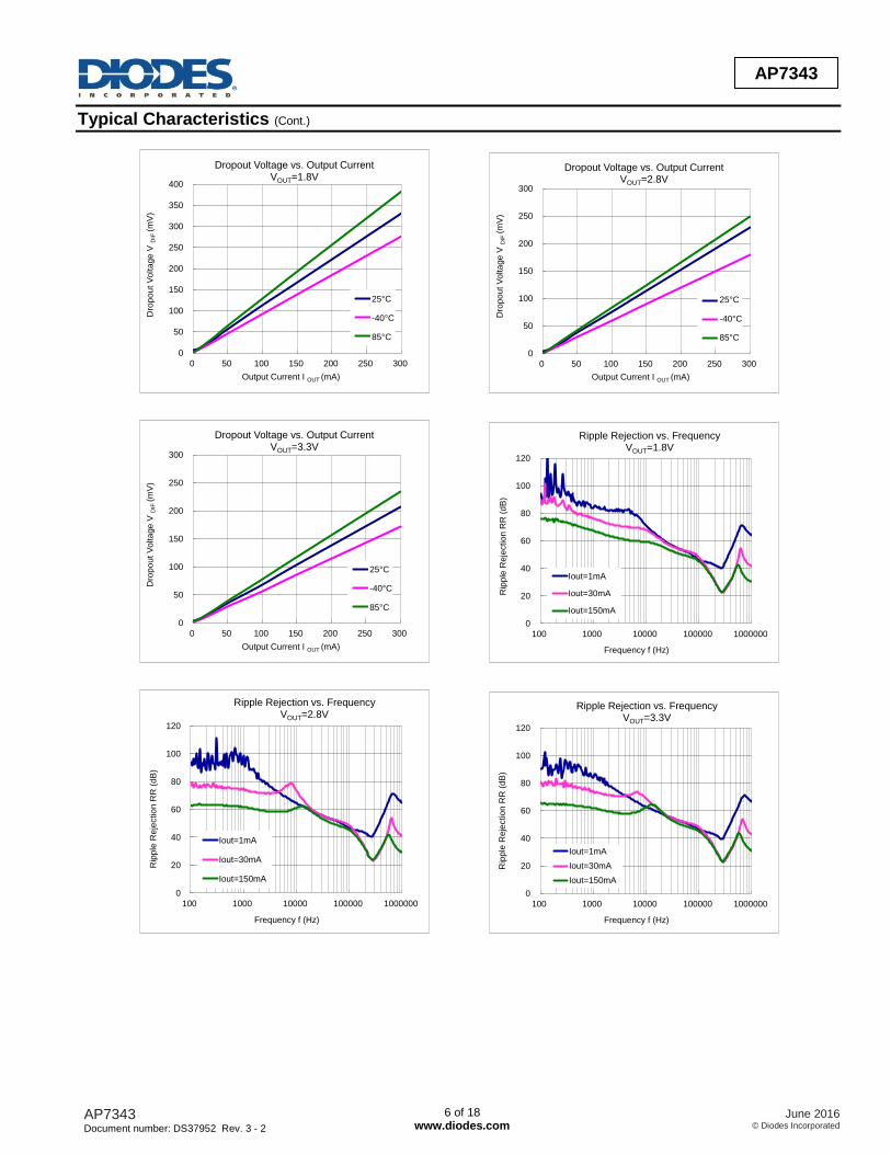
Line Transient Response Waveforms (IOUT = 30mA, tR = tF = 5μs, CIN = None, COUT1 = COUT2 = 1μF, TA = +25°C)
0
10
20
30
40
50
60
70
80
90
2.8 3.3 3.8 4.3 4.8 5.3
Rip
ple
Re
jectio
n R
R(d
B)
Input Voltage V IN (V)
Ripple Rejection vs. Input VoltageVOUT=2.8V
0.1KHz
1KHz
10KHz
100KHz
IOUT=1mA
0
10
20
30
40
50
60
70
80
90
2.8 3.3 3.8 4.3 4.8 5.3
Rip
ple
Reje
ctio
n R
R(d
B)
Input Voltage V IN (V)
Ripple Rejection vs. Input VoltageVOUT=2.8V
0.1KHz
1KHz
10KHz
100KHz
IOUT=30mA
VOUT = 1.8V
Time t (µs)
Output Voltage
Input Voltage
0 20 40 60 80 100
Ou
tpu
t V
olta
ge V
OU
T (V
)
1.80
1.79
1.81
5
4
3
Input V
olta
ge V
IN
(V
)
VOUT = 2.8V
Time t (µs)
Output Voltage
Input Voltage
0 20 40 60 80 100
Outp
ut V
oltage V
OU
T (V
)
2.80
2.79
2.81
5
4
3
Inp
ut V
olta
ge V
IN
(V
)
VOUT = 3.3V
Time t (µs)
Output Voltage
Input Voltage
0 20 40 60 80 100
Ou
tpu
t V
olta
ge V
OU
T (V
)
3.30
3.29
3.31
5
4
3
Inp
ut V
olta
ge V
IN
(V
)

AP7343 Document number: DS37952 Rev. 3 - 2
8 of 18 www.diodes.com
June 2016 © Diodes Incorporated
AP7343
Typical Characteristics (Cont.)
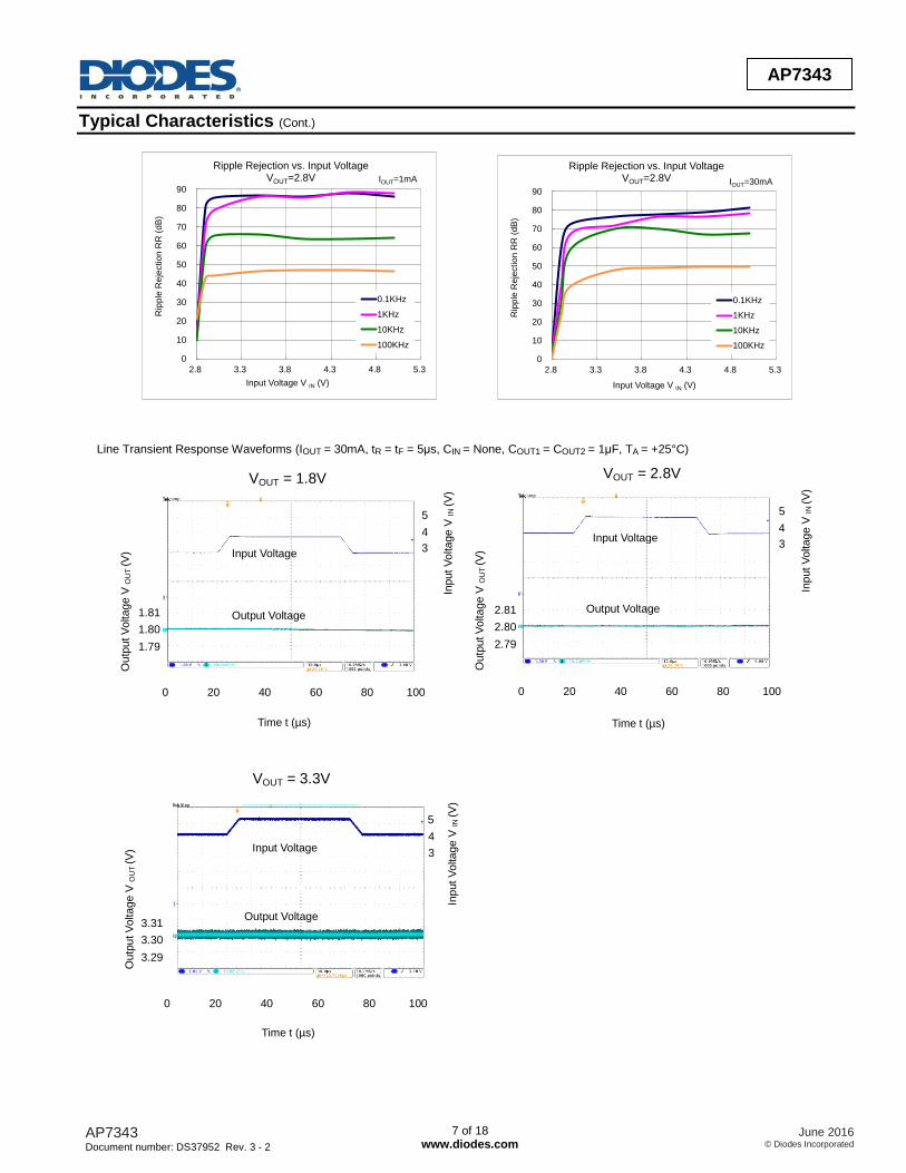
Load Transient Response Waveforms (VIN = VOUT+1V, CIN = 1μF, TA = +25°C)
VOUT = 1.8V
Time t (µs)
Output Voltage
Output Current
50mA 100mA
0 80 160 240 320 400
Ou
tpu
t V
olta
ge V
OU
T (V
)
150
100
50
0
COUT=1µF
Ou
tpu
t C
urr
ent I
OU
T (
mA
)
1.81
1.80
1.82
1.79
1.78
Time t (µs)
Output Voltage
Output Current
50mA 100mA
0 80 160 240 320 400
Ou
tpu
t V
olta
ge V
OU
T (V
)
150
100
50
0
COUT=4.7µF
Ou
tpu
t C
urr
ent I
OU
T (
mA
)
1.81
1.80
1.82
1.79
1.78
VOUT = 1.8V
Time t (µs)
Output Current
50mA 100mA
0 80 160 240 320 400
Outp
ut V
oltage V
OU
T (V
)
150
100
50
0
COUT=1µF
Outp
ut C
urr
ent I
OU
T (
mA
)
2.81
2.80
2.82
2.79
2.78
VOUT = 2.8V
Output Voltage
Time t (µs)
Output Current
50mA 100mA
0 80 160 240 320 400
Ou
tpu
t V
olta
ge V
OU
T (V
)
150
100
50
0
COUT=4.7µF
Outp
ut C
urr
ent I
OU
T (
mA
)
2.81
2.80
2.82
2.79
2.78
VOUT = 2.8V
Output Voltage
VOUT = 3.3V
Time t (µs)
Output Current
50mA 100mA
0 80 160 240 320 400
Ou
tpu
t V
olta
ge V
OU
T (V
)
150
100
50
0
COUT=1µF
Outp
ut C
urr
ent I O
UT (
mA
)
3.31
3.30
3.32
3.29
3.28 Output Voltage
VOUT = 3.3V
Time t (µs)
Output Voltage
Output Current
50mA 100mA
0 80 160 240 320 400
Ou
tpu
t V
olta
ge V
OU
T (V
)
150
100
50
0
COUT=4.7µF
Ou
tpu
t C
urr
ent I
OU
T (
mA
)
3.31
3.30
3.32
3.29
3.28
AP7343 Document number: DS37952 Rev. 3 - 2
9 of 18 www.diodes.com
June 2016 © Diodes Incorporated
AP7343
Typical Characteristics (Cont.)
Load Transient Response Waveforms (VIN = VOUT+1V, CIN = 1μF, TA = +25°C)
VOUT = 1.8V
Time t (µs)
Output Voltage
Output Current
1mA 300mA
0 80 160 240 320 400
Ou
tput V
oltage V
OU
T (V
)
400
200
0
COUT=1µF
Outp
ut C
urr
ent I
OU
T (
mA
)
1.85
1.80
1.90
1.75
1.70
Time t (µs)
Output Voltage
Output Current
1mA 300mA
0 80 160 240 320 400
Ou
tpu
t V
olta
ge V
OU
T (V
)
400
200
0
COUT=4.7µF
Ou
tpu
t C
urr
ent I
OU
T (
mA
)
1.85
1.80
1.90
1.75
1.70
VOUT = 1.8V
VOUT = 2.8V
Time t (µs)
Output Current
1mA 300mA
0 80 160 240 320 400
Ou
tpu
t V
olta
ge V
OU
T (V
)
400
200
0
COUT=1µF
Ou
tpu
t C
urr
ent I
OU
T (
mA
)
2.85
2.80
2.90
2.75
2.70 Output Voltage
VOUT = 2.8V
Time t (µs)
Output Current
1mA 300mA
0 80 160 240 320 400
Ou
tpu
t V
olta
ge V
OU
T (V
)
400
200
0
COUT=4.7µF
Ou
tpu
t C
urr
ent I
OU
T (
mA
)
2.85
2.80
2.90
2.75
2.70 Output Voltage
VOUT = 3.3V
Time t (µs)
Output Current
1mA 300mA
0 80 160 240 320 400
Outp
ut V
olta
ge V
OU
T (V
)
400
200
0
COUT=1µF
Ou
tpu
t C
urr
ent I
OU
T (
mA
)
3.35
3.30
3.40
3.25
3.20 Output Voltage
VOUT = 3.3V
Time t (µs)
Output Voltage
Output Current
1mA 300mA
0 80 160 240 320 400
Ou
tpu
t V
olta
ge V
OU
T (V
)
400
200
0
COUT=4.7µF
Ou
tpu
t C
urr
ent I
OU
T (
mA
)
3.35
3.30
3.40
3.25
3.20
AP7343 Document number: DS37952 Rev. 3 - 2
10 of 18 www.diodes.com
June 2016 © Diodes Incorporated
AP7343
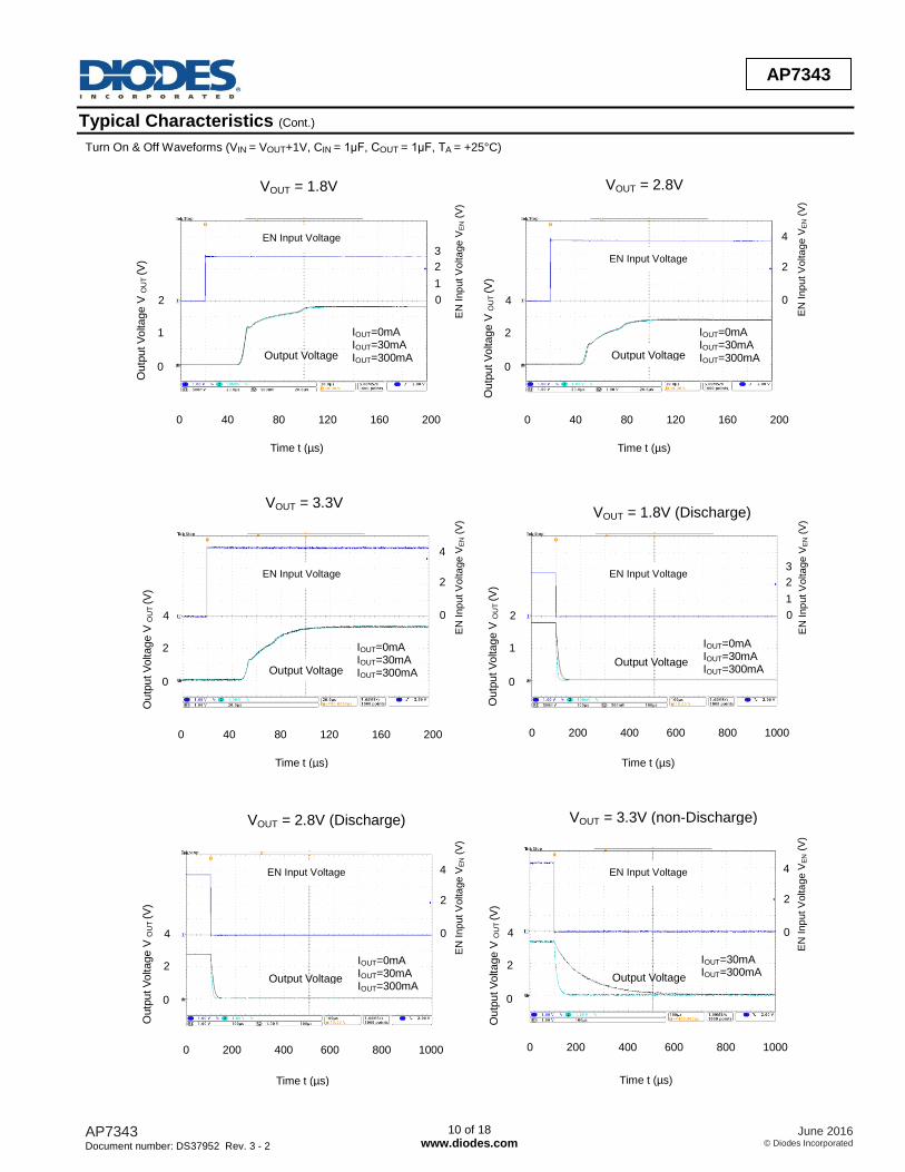
Typical Characteristics (Cont.)
Turn On & Off Waveforms (VIN = VOUT+1V, CIN = 1μF, COUT = 1μF, TA = +25°C)
VOUT = 1.8V
Time t (µs)
Output Voltage
CE Input Voltage
0 40 80 120 160 200
Outp
ut V
oltage V
OU
T (V
)
0
1
3
2
1
2
CE
In
put
Voltag
e V
CE (
V)
IOUT=0mA IOUT=30mA IOUT=300mA
0
VOUT = 2.8V
Time t (µs)
Output Voltage
CE Input Voltage
0 40 80 120 160 200
Outp
ut V
oltage V
OU
T (V
)
0
2
2
4
CE
In
put
Voltag
e V
CE (
V)
IOUT=0mA IOUT=30mA IOUT=300mA
0
4
VOUT = 3.3V
Time t (µs)
Output Voltage
CE Input Voltage
0 40 80 120 160 200
Ou
tpu
t V
olta
ge V
OU
T (V
)
0
2
2
4
CE
In
put V
oltag
e V
CE (
V)
IOUT=0mA IOUT=30mA IOUT=300mA
0
4
VOUT = 1.8V (Discharge)
Time t (µs)
Output Voltage
CE Input Voltage
Ou
tpu
t V
olta
ge V
OU
T (V
)
0
1
3
2
1
2
CE
In
put V
oltag
e V
CE (
V)
IOUT=0mA IOUT=30mA IOUT=300mA
0
0 200 400 600 800 1000
VOUT = 2.8V (Discharge)
Time t (µs)
Output Voltage
CE Input Voltage
Outp
ut V
oltage V
OU
T (V
)
0
2
2
4
CE
In
put V
oltag
e V
CE (
V)
IOUT=0mA IOUT=30mA IOUT=300mA
0
4
0 200 400 600 800 1000
VOUT = 3.3V (non-Discharge)
Time t (µs)
Output Voltage
CE Input Voltage
0 200 400 600 800 1000
Ou
tpu
t V
olta
ge V
OU
T (V
)
0
2
2
4
CE
In
put
Voltag
e V
CE (
V)
IOUT=30mA IOUT=300mA
0
4 EN Input Voltage
EN
Inp
ut V
olta
ge V
EN (
V)
EN
Inp
ut V
olta
ge V
EN (
V)
EN
Inp
ut V
olta
ge V
EN (
V)
EN
Inp
ut V
olta
ge V
EN (
V)
EN
Inp
ut V
olta
ge V
EN (
V)
EN
Inp
ut V
olta
ge V
EN (
V)
EN Input Voltage
EN Input Voltage
EN Input Voltage
EN Input Voltage
EN Input Voltage

AP7343 Document number: DS37952 Rev. 3 - 2
11 of 18 www.diodes.com
June 2016 © Diodes Incorporated
AP7343
Application Information
Output Capacitor
An output capacitor (COUT) is needed to improve transient response and maintain stability. The AP7343 is stable with very small ceramic output
capacitors. The ESR (equivalent series resistance) and capacitance drives the selection. If the application has large load variations, it is
recommended to utilize low-ESR bulk capacitors. It is recommended to place ceramic capacitors as close as possible to the load and the ground
pin and care should be taken to reduce the impedance in the layout.
Input Capacitor
To prevent the input voltage from dropping during load steps, it is recommended to utilize an input capacitor (CIN). A minimum 0.47μF ceramic
capacitor is recommended between VIN and GND pins to decouple input power supply glitch. This input capacitor must be located as close as
possible to the device to assure input stability and reduce noise. For PCB layout, a wide copper trace is required for both VIN and GND pins.
Enable Control
The AP7343 is turned on by setting the EN pin high, and is turned off by pulling it low. If this feature is not used, the EN pin should be tied to VIN pin
to keep the regulator output on at all times. To ensure proper operation, the signal source used to drive the EN pin must be able to swing above
and below the specified turn-on/off voltage thresholds listed in the Electrical Characteristics section.
Short Circuit Protection
When VOUT pin is short-circuit to GND, short circuit protection will be triggered and clamp the output current to approximately 60mA. This feature
protects the regulator from overcurrent and damage due to overheating.
Layout Considerations
For good ground loop and stability, the input and output capacitors should be located close to the input, output, and ground pins of the device. The
regulator ground pin should be connected to the external circuit ground to reduce voltage drop caused by trace impedance. Ground plane is
generally used to reduce trace impedance. Wide trace should be used for large current paths from VIN to VOUT, and load circuit.
ESR vs. Output Current
Ceramic type output capacitor is recommended for this series; however, the other output capacitors with low ESR also can be used. The relations
between IOUT (Output Current) and ESR of an output capacitor are shown below. The stable region is marked as the hatched area in the graph.
Measurement conditions: Frequency Band: 10Hz to 2MHz, Temperature: −40°C to +85°C.
0.001
0.01
0.1
1
10
100
0 50 100 150 200 250 300
ESR
(Ω
)
Output Current IOUT (mA)
ESR vs. Output CurrentAP7343-18
-40°C
85°C
0.001
0.01
0.1
1
10
100
0 50 100 150 200 250 300
ESR
(Ω
)
Output Current IOUT (mA)
ESR vs. Output CurrentAP7343-33
-40°C
85°C

AP7343 Document number: DS37952 Rev. 3 - 2
12 of 18 www.diodes.com
June 2016 © Diodes Incorporated
AP7343
Ordering Information (Note 12)
AP7343X - XXX XXX – XX
PackageOutput Discharge
FS4 : X2-DFN1010-4
(Type B)
W5: SOT25
7/7B : Tape & Reel
Packing
09 : 0.9VBlank : Non-dischargeD : Output Discharge
Output Voltage
10 : 1.0V105 : 1.05V
11 : 1.1V12 : 1.2V
13 : 1.3V135 : 1.35V
14 : 1.4V
185 : 1.85V
15 : 1.5V16 : 1.6V
20 : 2.0V21 : 2.1V
17 : 1.7V18 : 1.8V
19 : 1.9V
22 : 2.2V23 : 2.3V25 : 2.5V26 : 2.6V27 : 2.7V28 : 2.8V
285 : 2.85V29 : 2.9V
295 : 2.95V30 : 3.0V31 : 3.1V32 : 3.2V33 : 3.3V34 : 3.4V35 : 3.5V36 : 3.6V
Part Number Package
Code Packaging
7” Tape and Reel
Quantity Part Number Suffix
AP7343-XXXFS4-7B FS4 X2-DFN1010-4 (Type B) 10,000/Tape & Reel -7B
AP7343D-XXXFS4-7B FS4 X2-DFN1010-4 (Type B) 10,000/Tape & Reel -7B
AP7343-XXXW5-7 W5 SOT25 3,000/Tape & Reel -7
AP7343D-XXXW5-7 W5 SOT25 3,000/Tape & Reel -7
Note: 12. For packaging details, go to our website at http://www.diodes.com/products/packages.html.

AP7343 Document number: DS37952 Rev. 3 - 2
13 of 18 www.diodes.com
June 2016 © Diodes Incorporated
AP7343
Marking Information
(1) X2-DFN1010-4 (Type B)
Y : Year : 0~9
(Top View)
X : A~Z : Internal code
Y W X
XX XX : Identification Code
W : Week : A~Z : 1~26 week;
a~z : 27~52 week; z represents52 and 53 week
Part Number Package Identification Code
AP7343-09FS4-7B X2-DFN1010-4 (Type B) 7B
AP7343-10FS4-7B X2-DFN1010-4 (Type B) 7C
AP7343-105FS4-7B X2-DFN1010-4 (Type B) 7D
AP7343-11FS4-7B X2-DFN1010-4 (Type B) 7E
AP7343-12FS4-7B X2-DFN1010-4 (Type B) 7F
AP7343-135FS4-7B X2-DFN1010-4 (Type B) 7G
AP7343-15FS4-7B X2-DFN1010-4 (Type B) 7H
AP7343-18FS4-7B X2-DFN1010-4 (Type B) 7J
AP7343-185FS4-7B X2-DFN1010-4 (Type B) 7K
AP7343-22FS4-7B X2-DFN1010-4 (Type B) 7M
AP7343-25FS4-7B X2-DFN1010-4 (Type B) 7N
AP7343-28FS4-7B X2-DFN1010-4 (Type B) 7P
AP7343-285FS4-7B X2-DFN1010-4 (Type B) 7R
AP7343-295FS4-7B X2-DFN1010-4 (Type B) 7S
AP7343-30FS4-7B X2-DFN1010-4 (Type B) 7T
AP7343-31FS4-7B X2-DFN1010-4 (Type B) 7U
AP7343-32FS4-7B X2-DFN1010-4 (Type B) 7V
AP7343-33FS4-7B X2-DFN1010-4 (Type B) 7W
AP7343D-09FS4-7B X2-DFN1010-4 (Type B) 8B
AP7343D-10FS4-7B X2-DFN1010-4 (Type B) 8C
AP7343D-105FS4-7B X2-DFN1010-4 (Type B) 8D
AP7343D-11FS4-7B X2-DFN1010-4 (Type B) 8E
AP7343D-12FS4-7B X2-DFN1010-4 (Type B) 8F
AP7343D-13FS4-7B X2-DFN1010-4 (Type B) 8G
AP7343D-135FS4-7B X2-DFN1010-4 (Type B) 8H
AP7343D-14FS4-7B X2-DFN1010-4 (Type B) 8J
AP7343D-15FS4-7B X2-DFN1010-4 (Type B) 8K
AP7343D-16FS4-7B X2-DFN1010-4 (Type B) 8M
AP7343D-17FS4-7B X2-DFN1010-4 (Type B) 8N
AP7343D-18FS4-7B X2-DFN1010-4 (Type B) 8P
AP7343D-185FS4-7B X2-DFN1010-4 (Type B) 8R
AP7343D-19FS4-7B X2-DFN1010-4 (Type B) 8S
AP7343D-20FS4-7B X2-DFN1010-4 (Type B) 8T
AP7343D-21FS4-7B X2-DFN1010-4 (Type B) 8U
AP7343D-22FS4-7B X2-DFN1010-4 (Type B) 8V
AP7343D-23FS4-7B X2-DFN1010-4 (Type B) 8W
AP7343D-25FS4-7B X2-DFN1010-4 (Type B) 8X
AP7343D-26FS4-7B X2-DFN1010-4 (Type B) 8Y
AP7343D-27FS4-7B X2-DFN1010-4 (Type B) 8Z
AP7343D-28FS4-7B X2-DFN1010-4 (Type B) 6J
AP7343D-285FS4-7B X2-DFN1010-4 (Type B) 6K
AP7343D-29FS4-7B X2-DFN1010-4 (Type B) 6M
AP7343D-295FS4-7B X2-DFN1010-4 (Type B) 6N
AP7343D-30FS4-7B X2-DFN1010-4 (Type B) 6P
AP7343D-31FS4-7B X2-DFN1010-4 (Type B) 6R
AP7343D-32FS4-7B X2-DFN1010-4 (Type B) 6S
AP7343D-33FS4-7B X2-DFN1010-4 (Type B) 6T
AP7343D-34FS4-7B X2-DFN1010-4 (Type B) 6U
AP7343D-35FS4-7B X2-DFN1010-4 (Type B) 6V
AP7343D-36FS4-7B X2-DFN1010-4 (Type B) 6W

AP7343 Document number: DS37952 Rev. 3 - 2
14 of 18 www.diodes.com
June 2016 © Diodes Incorporated
AP7343
Marking Information (Cont.)
(2) SOT25
Part Number Package Type Identification Code
AP7343-09W5-7 SOT25 7B
AP7343-10W5-7 SOT25 7C
AP7343-105W5-7 SOT25 7D
AP7343-11W5-7 SOT25 7E
AP7343-12W5-7 SOT25 7F
AP7343-135W5-7 SOT25 7G
AP7343-15W5-7 SOT25 7H
AP7343-18W5-7 SOT25 7J
AP7343-185W5-7 SOT25 7K
AP7343-22W5-7 SOT25 7M
AP7343-25W5-7 SOT25 7N
AP7343-28W5-7 SOT25 7P
AP7343-285W5-7 SOT25 7R
AP7343-295W5-7 SOT25 7S
AP7343-30W5-7 SOT25 7T
AP7343-31W5-7 SOT25 7U
AP7343-32W5-7 SOT25 7V
AP7343-33W5-7 SOT25 7W
AP7343D-09W5-7 SOT25 8B
AP7343D-10W5-7 SOT25 8C
AP7343D-105W5-7 SOT25 8D
AP7343D-11W5-7 SOT25 8E
AP7343D-12W5-7 SOT25 8F
AP7343D-13W5-7 SOT25 8G
AP7343D-135W5-7 SOT25 8H
AP7343D-14W5-7 SOT25 8J
AP7343D-15W5-7 SOT25 8K
AP7343D-16W5-7 SOT25 8M
AP7343D-17W5-7 SOT25 8N
AP7343D-18W5-7 SOT25 8P
AP7343D-185W5-7 SOT25 8R
AP7343D-19W5-7 SOT25 8S
AP7343D-20W5-7 SOT25 8T
AP7343D-21W5-7 SOT25 8U
AP7343D-22W5-7 SOT25 8V
AP7343D-23W5-7 SOT25 8W
AP7343D-25W5-7 SOT25 8X
AP7343D-26W5-7 SOT25 8Y
AP7343D-27W5-7 SOT25 8Z
AP7343D-28W5-7 SOT25 6J
AP7343D-285W5-7 SOT25 6K
AP7343D-29W5-7 SOT25 6M
AP7343D-295W5-7 SOT25 6N
AP7343D-30W5-7 SOT25 6P
AP7343D-31W5-7 SOT25 6R
AP7343D-32W5-7 SOT25 6S
AP7343D-33W5-7 SOT25 6T
AP7343D-34W5-7 SOT25 6U
AP7343D-35W5-7 SOT25 6V
AP7343D-36W5-7 SOT25 6W
1 2 3
5 74XX : Identification Code
W : Week : A to Z : 1 to 26 week;
X : Internal Code
(Top View)
Y : Year 0 to 9
a to z : 27 to 52 week; z represents52 and 53 week
XX Y W X

AP7343 Document number: DS37952 Rev. 3 - 2
15 of 18 www.diodes.com
June 2016 © Diodes Incorporated
AP7343
Package Outline Dimensions
Please see http://www.diodes.com/package-outlines.html for the latest version.
(1) X2-DFN1010-4 (Type B)
(2) SOT25
X2-DFN1010-4 (Type B)
Dim Min Max Typ
A - 0.40 0.39
A1 0.00 0.05 0.02
A3 - - 0.13
b 0.20 0.30 0.25
D 0.95 1.05 1.00
D2 0.43 0.53 0.48
E 0.95 1.05 1.00
E2 0.43 0.53 0.48
e - - 0.65
k - - 0.17
L 0.20 0.30 0.25
L1 0.02 0.12 0.07
z - - 0.050
All Dimensions in mm
SOT25
Dim Min Max Typ
A 0.35 0.50 0.38
B 1.50 1.70 1.60
C 2.70 3.00 2.80
D - - 0.95
H 2.90 3.10 3.00
J 0.013 0.10 0.05
K 1.00 1.30 1.10
L 0.35 0.55 0.40
M 0.10 0.20 0.15
N 0.70 0.80 0.75
0° 8° -
All Dimensions in mm
A A1A3
Seating Plane
D
E
z(4x) b(4x)
e
L(4x)
L1(4x)E2 D2
4-C
0.18
k
Pin #1 ID
R0.050
A
M
JLD
B C
H
KN

AP7343 Document number: DS37952 Rev. 3 - 2
16 of 18 www.diodes.com
June 2016 © Diodes Incorporated
AP7343
Suggested Pad Layout
Please see http://www.diodes.com/package-outlines.html for the latest version.
(1) X2-DFN1010-4 (Type B)
(2) SOT25
Dimensions Value
(in mm)
C 0.650
X 0.350
X1 0.112
X2 0.530
X3 1.00
Y 0.350
Y1 0.530
Y2 1.100
Dimensions Value
Z 3.20
G 1.60
X 0.55
Y 0.80
C1 2.40
C2 0.95
Y2
X3
C
X
Y
X1
X2
Y1
X
Z
Y
C1
C2C2
G

AP7343 Document number: DS37952 Rev. 3 - 2
17 of 18 www.diodes.com
June 2016 © Diodes Incorporated
AP7343
Tape Orientation
For AP7343-XXXFS4-7B & AP7343D-XXXFS4-7B
For AP7343-XXXW5-7 & AP7343D-XXXW5-7
Note: 13. The taping orientation of the other package type can be found on our website at http://www.diodes.com/datasheets/ap02007.pdf.

AP7343 Document number: DS37952 Rev. 3 - 2
18 of 18 www.diodes.com
June 2016 © Diodes Incorporated
AP7343
IMPORTANT NOTICE DIODES INCORPORATED MAKES NO WARRANTY OF ANY KIND, EXPRESS OR IMPLIED, WITH REGARDS TO THIS DOCUMENT, INCLUDING, BUT NOT LIMITED TO, THE IMPLIED WARRANTIES OF MERCHANTABILITY AND FITNESS FOR A PARTICULAR PURPOSE (AND THEIR EQUIVALENTS UNDER THE LAWS OF ANY JURISDICTION). Diodes Incorporated and its subsidiaries reserve the right to make modifications, enhancements, improvements, corrections or other changes without further notice to this document and any product described herein. Diodes Incorporated does not assume any liability arising out of the application or use of this document or any product described herein; neither does Diodes Incorporated convey any license under its patent or trademark rights, nor the rights of others. Any Customer or user of this document or products described herein in such applications shall assume all risks of such use and will agree to hold Diodes Incorporated and all the companies whose products are represented on Diodes Incorporated website, harmless against all damages. Diodes Incorporated does not warrant or accept any liability whatsoever in respect of any products purchased through unauthorized sales channel. Should Customers purchase or use Diodes Incorporated products for any unintended or unauthorized application, Customers shall indemnify and hold Diodes Incorporated and its representatives harmless against all claims, damages, expenses, and attorney fees arising out of, directly or indirectly, any claim of personal injury or death associated with such unintended or unauthorized application. Products described herein may be covered by one or more United States, international or foreign patents pending. Product names and markings noted herein may also be covered by one or more United States, international or foreign trademarks. This document is written in English but may be translated into multiple languages for reference. Only the English version of this document is the final and determinative format released by Diodes Incorporated.
LIFE SUPPORT Diodes Incorporated products are specifically not authorized for use as critical components in life support devices or systems without the express written approval of the Chief Executive Officer of Diodes Incorporated. As used herein: A. Life support devices or systems are devices or systems which: 1. are intended to implant into the body, or
2. support or sustain life and whose failure to perform when properly used in accordance with instructions for use provided in the labeling can be reasonably expected to result in significant injury to the user.
B. A critical component is any component in a life support device or system whose failure to perform can be reasonably expected to cause the failure of the life support device or to affect its safety or effectiveness. Customers represent that they have all necessary expertise in the safety and regulatory ramifications of their life support devices or systems, and acknowledge and agree that they are solely responsible for all legal, regulatory and safety-related requirements concerning their products and any use of Diodes Incorporated products in such safety-critical, life support devices or systems, notwithstanding any devices- or systems-related information or support that may be provided by Diodes Incorporated. Further, Customers must fully indemnify Diodes Incorporated and its representatives against any damages arising out of the use of Diodes Incorporated products in such safety-critical, life support devices or systems. Copyright © 2016, Diodes Incorporated www.diodes.com