Embed Size (px)
Citation preview
Declaration
I hereby declare that the work entitled, “Study on physical properties of ZnS thin films
prepared by chemical bath deposition” is the original work done by me under the
supervision of Dr. V. Senthil Kumar, Associate Professor, Department of Physics,
Karpagam University, Coimbatore as a part of my Ph.D. work during the period from 2009 to
2013. I hereby declare that this manuscript or its contents have not formed a part of any other
paper or thesis and also has not been submitted elsewhere for publication.
Your’s truly,
S. Kalyanasundaram

Author Details
1. S. KalyanasundaramPh.D. Scholar (part time)Department of Physics,Karpagam University,Coimbatore-641 021Tamil Nadu88838 [email protected]
2. Dr. V. Senthil KumarAssociate Professor,Department of Physics,Karpagam University,Coimbatore-641 021Tamil Nadu94439 [email protected]
3. Dr. K. PanneerselvamAssociate Professor,Department of Physics,Karpagam University,Coimbatore-641 021Tamil Nadu98429 21367

Study on physical properties of ZnS thin films prepared by chemical bath deposition
S. Kalyanasundaram*, Dr. K. Panneerselvam, Dr. V. Senthil Kumar
Department of Physics, Karpagam University, Coimbatore, Tamilnadu.
Abstract
ZnS thin films have been deposited by chemical bath deposition method using
ammonia as a complexing agent with various deposition times. The morphological, optical,
structural and compositional analysis of films have been investigated by SEM, UV
spectroscopy; XRD and EDAX. The XRD analysis of as deposited films shows that the films
were cubic structure, the grain size of the film increases with increase in the deposition time.
UV spectroscopy studies show good transmission characteristic with an average
transmittance of 70-85%. The band gap energy values of ZnS films increased from 3.84 to
3.90 eV with increasing deposition time.
Key words: Zinc compounds, CBD, XRD, SEM, EDAX, UV spectroscopy.
1. Introduction
Traditionally CdS buffer layers deposited by chemical bath deposition have been used
in thinfilm solar cells (TFSC) to obtain high conversion efficiency. But CdS thin films when
utilized in large scale solar cell production could raise environmental problems due to high
amount of Cd compounds waste (Sartale 2005, Jhonston 2002). The search for alternative to
Cd-free buffer layers is the subject of interest and many efforts to overcome these difficulties
are still ongoing (Asenjo 2008, Puspitasari 2008). Recently the nano and polycrystalline ZnS
thin films have attracted researchers as they play crucial role in photovoltaic technology and
opto-electronics devices (So Ra Kang 2010). Zinc sulphide thin films are the promising
materials for its use in various application devices. In opto electronics it can be used as light

emitting diode in the blue to ultraviolet spectral region due to its wide band gap of 3.7 eV at
room temperature (Yamaga 1998). In the area of optics, ZnS can be used as a reflector and
dielectric filter because of its high refractive index (2.35) and its high transmittance in the
visible range respectively (Ruffner 1989, Ledger 1979). Zinc sulphide is less toxic, efficient,
cost effective material and has good transparency.
ZnS thin films are synthesized by different methods such as thermal evaporation
(Dimitrova 2000), spray pyrolysis (Mustafa 2007), sputtering (Shao 2003), chemical vapor
deposition [Icimura 1999], successive ionic layer adsorption and reaction (SILAR) (Nomura
1995), and the metal organic vapour phase epitaxy (MOVPE) (Roy 2006, Dona 1995).
Among these, a very attractive method for producing ZnS thin films due to the possibility of
large area deposition at low cost is the so called chemical bath deposition (CBD) method.
Ammonia and hydrazine are popular choices as the complexing agent in the CBD of ZnS thin
films. In addition tri sodium citrate can significantly improve the quality of the ZnS films
obtained (Gumus 2005).
In this paper we report some studies of chemical bath deposition of ZnS thin films
from NH3/SC (NH2)2/Zn (CH3Coo)3 solutions. The CBD ZnS thin films characterisation
including structural, compositional and optical are shown.
2. Experimental work
Using CBD technique Zinc sulphide thin films are prepared on glass substrates by
various deposition times. Aqueous solution of 10 ml, 0.2 M of Zinc acetate Zn(CH3COO)2,
10 ml of 0.6 M thiourea SC(NH2)2, 10 ml tri sodium citrate and 5 ml ammonia were used to
prepare ZnS thin films. The solution is continuously stirred for several minutes and it
becomes clear and homogeneous. Deionised water was added to make the solution up to 50
ml. The pH of the solution is maintained as 8.5. The glass substrates were first cleaned in
pure water, isopropyl alcohol, and double distilled water. The cleaned substrates (25 mm x 75
mm) were immersed vertically in the bath. The temperature of the bath was set at 80o C for
all the deposited ZnS thin films.
A Bruker AXS D8 advance x-ray diffratometer with vertical goniometer fitted with
copper radiation (=5406A) was used for the structural analysis of thin films coated with
different deposition times. The surface morphology of ZnS thin films was studied using a
scanning electron microscope (JEOL Model JSM - 6390LV), Energy dispersive spectrometer
(JEOL Model JED – 2300) confirmed the composition of the constituents.
3. Results and discussions
The X-ray diffraction (XRD) profiles of ZnS thin films deposited at various
deposition times (Table 1) are shown in fig1,2 and 3. Table 1: Preparatory conditions of the
thin films of chemical baths.
Chemical
baths
Thin film Temperature
( C)⁰
pH Deposition Time
(minutes)
Bath 1 A 80 8.5 30
Bath 2 B 80 8.5 45
Bath 3 C 80 8.5 60

Figure 1: XRD pattern of thin film A
Figure 2: XRD pattern of Thin film B
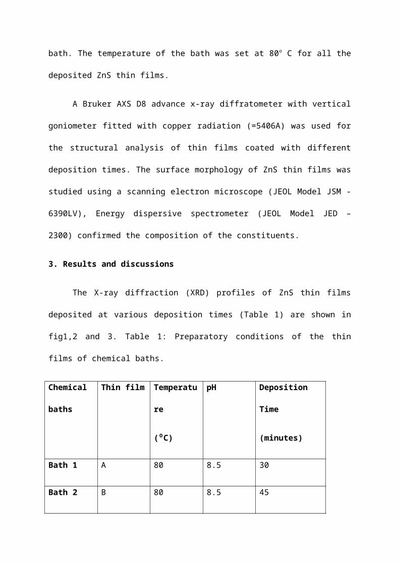
Figure 3: XRD pattern of Thin film C
Generally ZnS crystals exist in two forms, cubic (Zinc blende) and hexagonal (wurtzite). The
cubic form is stable at room temperature while wurtzite the less dense hexagonal form is
stable at high temperature (Berger 1997). ZnS films exhibited peaks corresponding to the
(111), (220) plane of the cubic ZnS phase and exactly matching with JCPDS PDF 65-1691
with lattice parameter of 5.41 A° and cell volume of 158.4 A° . The matching of standard and
observed 2θ values with cubic and hexagonal faces are depicted in table 2 from which is it
concluded that deposited ZnS thin films are of cubic structure.
Table 2: The comparison of the different planes with 2θ values with cubic and hexagonal
structures for CBD-ZnS thin films deposited with different deposition time. The peaks can be
assigned to both cubic and hexagonal ZnS phases of the planes using [JCPDS data file No.:
65-1691 (ZnS/cubic)]. [JCPDS data file No.: 72-0163 (ZnS/Hexagonal)]

Thin films Cubic Hexagonal Measured
angle (2θ)
Plane (h k l) Angle (2θ) Plane (h k l) Angle (2θ)
A
B
C
(1 1 1)
(2 2 0)
(1 1 1)
(2 2 0)
(1 1 1)
(2 2 0)
28.550
47.489
28.550
47.489
28.550
47.489
(0 0 8)
(1 0 1 1)
(0 0 8)
(1 0 1 1)
(0 0 8)
(1 0 1 1)
28.587
48.618
28.587
48.618
28.587
48.618
28.496
47.504
28.535
47.510
28.577
47.509
The film prepared with deposition time 30 min are amorphous as well as highly transparent.
When the deposition time increases the intensity of the ZnS (111) peak increases indicating a
better crystallinity. This behaviour is explained as follows: When the deposition time
increases the thickness of the ZnS film increases and the crystallinity is improved. The
diffraction peaks become slightly sharper and their intensity is relatively enhanced with

Wavelength (nm)
Transm
ittance
cba
increasing deposition time while their location did not changed significantly. The high noise
content of XRD graph did not allow identification of other phases. The average grain size of
the ZnS films can be estimated from scherrer formula : D = 0.9λ / β cosθ, where λ is the X-
ray wavelength of 0.5406 nm, β is the full width at half maximum, and θ is the Bragg
diffraction angel (Ladar 2007). The calculated average grain sizes were 12.07, 14.92, and
19.01 nm for the films coated at deposition time 30, 45 and 60 minutes respectively.
Figure 4 shows the optical transmittance spectra of ZnS thin films under different
deposition time intervals.
Figure 4: Transmittance spectra of thinfilms A,B,C
It is significant to note that these ZnS films were highly transparent in the visible region and
their transmittance was found to be over 70%. The thickness of ZnS films was dependent on
both the deposition time (30 to 60 minutes) and concentration of thiourea (upto 0.6 M) which
in turn results in decreasing trend for the transmittance of ZnS films from 85% to 70% in the
wavelength range of 600-800 nm. For a deposition time of 30 minutes, the transmittance
attained a maximum of 85% at a wavelength of 700nm. The transmittance of ZnS films was

inversely proportional to the deposition time which means at a short deposition time, higher
transmittance was observed that is highly desirable for enhancing the short circuit current.
The absorption were analyzed using the well known relation for near edge optical
absorption of semi conductors:
Αhυ = k (hυ - Eg)n/2,
Where k' is a constant, n is a constant equal to 1 for direct band gap semiconductors
and 4 for indirect band gap semiconductor materials. The variation of α2 versus hυ in Figure
5 is linear at the absorption edge, which confirms that ZnS is a direct band gap
semiconductor.
Figure 5: Band gap of A, B, C
3 40.00E+000
5.00E+014
1.00E+015
1.50E+015
2.00E+015
2.50E+015
3.00E+015
3.50E+015
(ahv
)2
hv (eV)
Extrapolating the straight line portion of the α2 versus hυ plot to zero absorption coefficient
value gives the band gap energy Eg. (Lokhande 2005), the estimated band gap values are
listed in the table 3.
Table 3: Estimated band gap values
Thin films Deposition Time (minutes) Band gap (eV)
A 30 3.84
B 45 3.88
C 60 3.90
The band gap values of the deposited thin films increases than that of the value of the
bulk ZnS (3.6 ev), which could be attributed to quantum confinement effects due to the small
grain sizes of the polycrystalline films.
The scanning electron micrographs of the deposited ZnS thin films are shown in
Figures 6, 7 & 8 of magnification x 5000.
Figure 6: SEM image of Thin film A

Figure 7: SEM image of thin film B
Figure 8: SEM image of thin film C
The surface of the thin film with deposition time 30 minutes seems to have a coarser surface
when compared to the surface of the thin films with deposition time 45 and 60 minutes. The
surface of the thin film with deposition time 30 minutes containing particles of size 0.5 to 1
micron. The smoothness of the film increases with the increase in the deposition time. The
particles with different contrast on the top of the film are due to the free particles which are
sitting on the films and they are not attached with the films, also there is reduce in the free
particles with increase in the deposition time is found. This might be the reason for the
smoothness of the films. The films with coarser surface (deposition time 30 and 45 minutes)
have discontinuities.

The Figure 9 shows the EDAX result of ZnS thin film with deposition time 30 minutes.
EDAX analysis confirms the presence of zinc and sulphur in ZnS thinfilm with composition
Zn1.05, S0.95.
Figure 9: EDAX analysis for thin film A
The proportion of the constituent elements measured was Zn = 52.68% and S = 47.32%. The
composition was near stoichiometric films can be obtained from the single and economic
CBD technique. EDAX spectrum also shows that prepared films are free from impurities.
The presence of silicon (Si) and oxygen (O) are due to glass substrates (Johnson 2002, Afifi
1995).
4. Conclusion
ZnS thin films have been successfully deposited by chemical bath deposition
technique with different deposition time. Our experiment, XRD studies show formation of
pure ZnS films cubic structure. The crystallinity of the films and the average grain size are
increased with increasing deposition time from 30 minutes to 60 minutes. The film shows
better optical transmission (70-85%) in the visible region. The optical transmission of the
film decreased with increase in deposition time. The calculated band gap value are in the

range of 3.8 - 3.9 eV, which will be very useful for solar cell. The morphology of the
deposited films has been found as smooth and the films with coarser surface have
discontinuities. The chemical constituents and their compositions of the films have been
estimated by the energy dispersive X-ray analysis. The deposited films are identified as Zn 1.05
S 0.95.
References
1. Afifi, H. H., Mohamaoud, S. A., and Ashour, A. (1995) “Effect of some spray pyrolysis
parameters on electrical and optical properties of ZnS films”, Thin Solid Films, 248 :
253-256.
2. Asenjo, B., Chapparo, A. M., Gutierrez, M. T., Herrero, J., and Klaer, “J. (2008) Study
of CuInS2/ZnS/ZnO solar cells, with chemically deposited ZnS buffer layers from acidic
solutions”, Solar Energy materials and Solar cells. 92 (3): 302.
3. Berger, L. I. (1997) “Semiconductor materials”, newyork, CRC press.
4. Dimitrova, J. Tate, (2000) “Synthesis and characterisation of some ZnS based thinfilm
phosphors for electroluminescent device applications”, Thin Solid Films.365 (1) : 134-
138.
5. Dona, J. M., and Herrero, J. (1995) “Chemical bath codeposited CdS-ZnS film
characterization”, Thin Solid Films. 268 : 5-12.
6. Gumus, C., Ulutas, C., Esen, R., Ozkendir, O. M., and Utuktepe, Y. (2005) “Preparation
and characterization of crystalline MnS thin films by chemical bath deposition”, Thin
Solid Films. 492: 1-5.
7. Icimura, M., Goto, F., Ono, Y., and Arai, E. (1999) “Deposition of CdS and ZnS from
aqueous solutions by a new photochemical technique”, J. Cryst. Growth. 198-199 (Part-
I) : 308-312.
8. Jhonston, D. A., Carletto, M. H., Reddy, K. T. R., Forbes, I., and Miles,R. W. (2002)

“Chemical bath deposition of zinc sulfide based buffer layers using low toxicity
materials”, Thin Solid Films, 403-404: 102-106.
9. Johnson, D. A., Corletto, M. H., Reddy, K. T. R., Forbes I., and Miles, R. W. (2002)
“Chemical bath deposition of zinc sulfide based buffer layers using low toxicity
materials”, Thin solid Films 403-404 : 102-106.
10. Ladar, M., Popovici, E. J., Baldea, I., Grech, R., and Inderea, E. (2007) “Studies on
chemical bath deposited zinc sulphide thin films with special optical properties”, J.
Alloys Compund, 434 : 697-700.
11. Ledger, A. M. (1979), “Inhomogeneous interface laser mirror coatings”, Appl. Opt. 18:
2979-2989.
12. Lokhande, C. D., Lee, E. H., Jung, K. D., and Joo, Q. S. (2005) “Ammonia-free
chemical bath method for deposition of microcrystalline cadmium selenide films”,
Materials Chemistry and Physics. 91: 200-204.
13. Mustafa, O., Bedir, M., Ocak, S., and Yildirim, R. G. (2007) “The role of growth
parameters on structural, morphology and optical properties of sprayed ZnS thin films, J.
Mater. Sci. Mater. Electron”, 18 (5) 505-512.
14. Nomura, R., Murai, T., Toyosaki, T., and Matsuda, H. (1995) “Single-source MOVPE
growth of zinc sulfide thin films using zinc dithiocarbamate complexes”, Thin Solid
Films. 271 (1-2) : 4-7.
15. Puspitasari, I., Gujar, T. P., Jung, K. D., and Joo, O. S. (2008) “Simple chemical method
for nanoporous network of In2S3 platelets for buffer layer in CIS solar cell, J. Mater.
Process. Technol”, 201 (1-3) 775-779.
16. Roy, P., Ota, J. R., and Srivastava, S. K. (2006) “Crystalline ZnS thin films by chemical
bath deposition method and its characterization”, Thin Solid Films. 515 (4) : 1912-1917.
17. Ruffner, J. A., Hilmel, M. D., Mizrahi, V., Stegeman, G. I., and Gibson, U. (1989)

“Effects of low substrate temperature and ion assisted deposition on composition, optical
properties, and stress of ZnS thin films”, J. Appl. Opt: 28 : 5209-5214.
18. Sartale, S. D., Sankapal, B. R., Lux-Steiner, M., and Ennaoui, A. (2005) “Preparation of
nanocrystalline ZnS by a new chemical bath deposition route”, Thin solid films. 480-
481: 168-172.
19. Shao, L. XChang, ., K. H., and Hwang, H. L. (2003) “Zinc sulfide thin films deposited
by RF reactive sputtering for photovoltaic applications” Appl. Surf. Sci. 212-213 (SPEC)
: 305-310.
20. So Ra Kang, Seung Wook Shi, Doo Sun Choi, Mohalkar, A. V., Jong-Ha Moon, and Jin
Hyeok Kim, (2010), “Effect of pH on the characteristics of nanocrystalline ZnS thin
films prepared by CBD method in acidic medium”, Current Applied Physics 10 : S473-
S477.
21. Yamaga, S., Yoshokawa, A., and Kasain, H., (1998) “Electrical and optical properties of
donor doped ZnS films grown by low-pressure MOCVD”, J.Crystal Growth. 86: 252-
256.


![The interaction of metal oxide surfaces with complexing ...1].pdf · Coordination Chemistry Reviews 196 (2000) 31–63 The interaction of metal oxide surfaces with complexing agents](https://img.pdfslide.net/doc/110x75/5ea6bb15b8499e332c7ba317/the-interaction-of-metal-oxide-surfaces-with-complexing-1pdf-coordination.jpg)