Embed Size (px)
Citation preview
Verilog Appendix
AA.1 Introduction
This appendix gives a quick introduction to the Verilog Hardware Description Language (HDL). There are many texts on Verilog ([Smith00, Thomas02, Ciletti99] and others) that provide a more in-depth treatment. The IEEE standard itself is quite readable as well as authoritative [IEEE1364-01]. Many books treat Verilog as a programming language, which is not the best way of viewing it. Verilog is better understood as a shorthand for describing digital hardware. It is best to begin your design process by planning, on paper or in your mind, the hardware you want. (For example, the MIPS processor consists of an FSM controller and a datapath built from registers, adders, multiplexers, etc.) Then, write Verilog that implies that hardware to a synthesis tool. A common error among beginners is to write a program without thinking about the hardware that is implied. If you don’t know what hardware you are implying, you are almost certain to get something that you didn’t want. Sometimes this means extra latches appearing in your circuit in places you didn’t expect. Other times, it means that the circuit is much slower than required or it takes far more gates than it would have if it were more carefully described. The Verilog language was developed by Gateway Design Automation as a propriety language for logic simulation in 1984. Gateway was acquired by Cadence in 1989 and Verilog was made an open standard in 1990 under the control of Open Verilog International. The language, with some revisions, became an IEEE standard in 1995 and was updated in 2001. This appendix is consistent with the 2001 standard. As mentioned in Section 1.8.4, there are two general styles of description: behavioral and structural. Structural Verilog describes how a module is composed of simpler modules or basic primitives such as gates or transistors. Behavioral Verilog describes how the outputs are computed as functions of the inputs. There are two general types of statements used in behavioral Verilog. Continuous assignment statements necessarily imply combinational logic1) because the output on the left side is a function of the inputs on the right side. Always blocks can imply combinational logic or sequential logic, depending on how they are used. It is good practice to partition your design into
1) Recall that the outputs of combinational logic depend only on the present inputs, while outputs of sequential logic depend on both past and present inputs. In other words, combinational logic is memoryless, while sequential logic has memory or state.
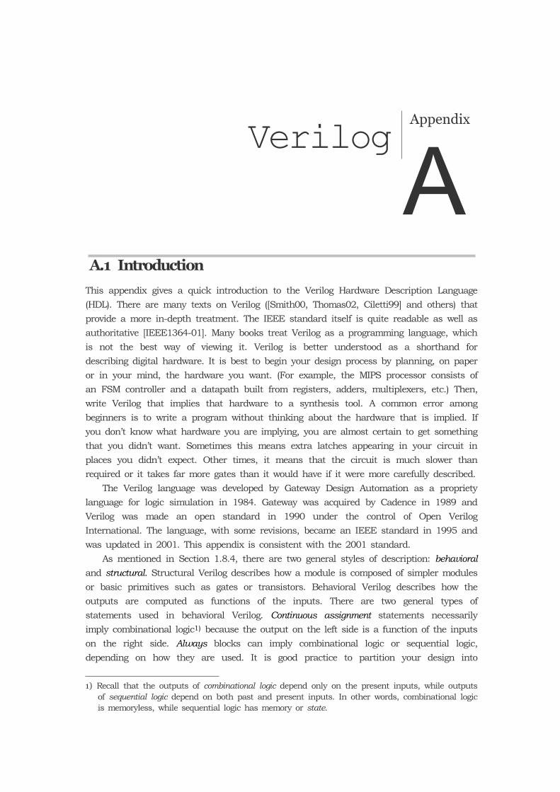
module adder ( input [31:0] a, input [31:0] b, output [31:0] y); assign y = a + b;endmodule
A.2 Behavioral Modeling with Continuous Assignments
A.2.1 Bitwise Operators
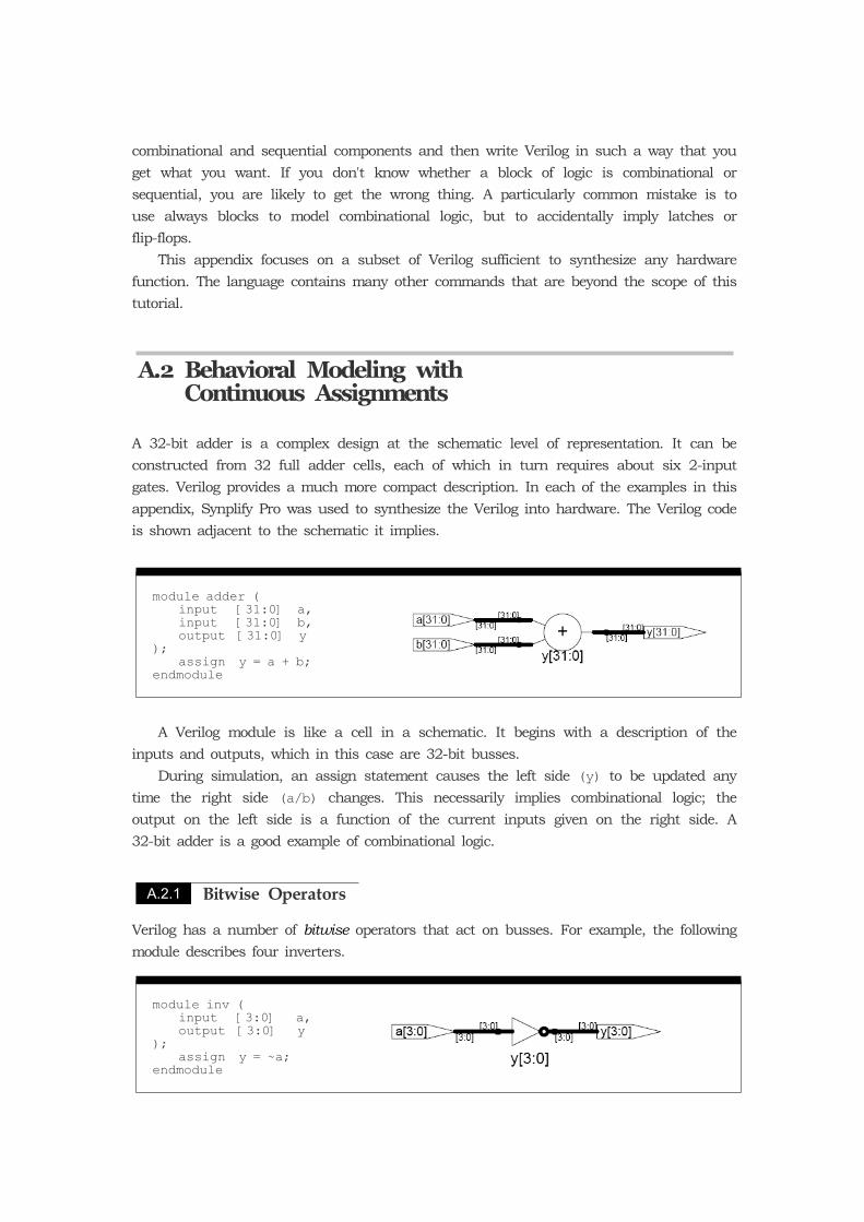
module inv ( input [3:0] a, output [3:0] y); assign y = ~a;endmodule
combinational and sequential components and then write Verilog in such a way that you get what you want. If you don't know whether a block of logic is combinational or sequential, you are likely to get the wrong thing. A particularly common mistake is to use always blocks to model combinational logic, but to accidentally imply latches or flip-flops. This appendix focuses on a subset of Verilog sufficient to synthesize any hardware function. The language contains many other commands that are beyond the scope of this tutorial.
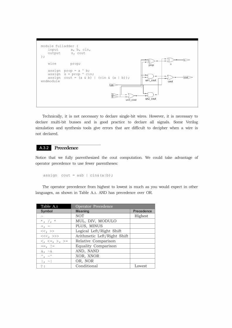
A 32-bit adder is a complex design at the schematic level of representation. It can be constructed from 32 full adder cells, each of which in turn requires about six 2-input gates. Verilog provides a much more compact description. In each of the examples in this appendix, Synplify Pro was used to synthesize the Verilog into hardware. The Verilog code is shown adjacent to the schematic it implies.
A Verilog module is like a cell in a schematic. It begins with a description of the inputs and outputs, which in this case are 32-bit busses. During simulation, an assign statement causes the left side (y) to be updated any time the right side (a/b) changes. This necessarily implies combinational logic; the output on the left side is a function of the current inputs given on the right side. A 32-bit adder is a good example of combinational logic.
Verilog has a number of bitwise operators that act on busses. For example, the following module describes four inverters.
A.2.2 Comments and White Space
A.2.3 Reduction Operators
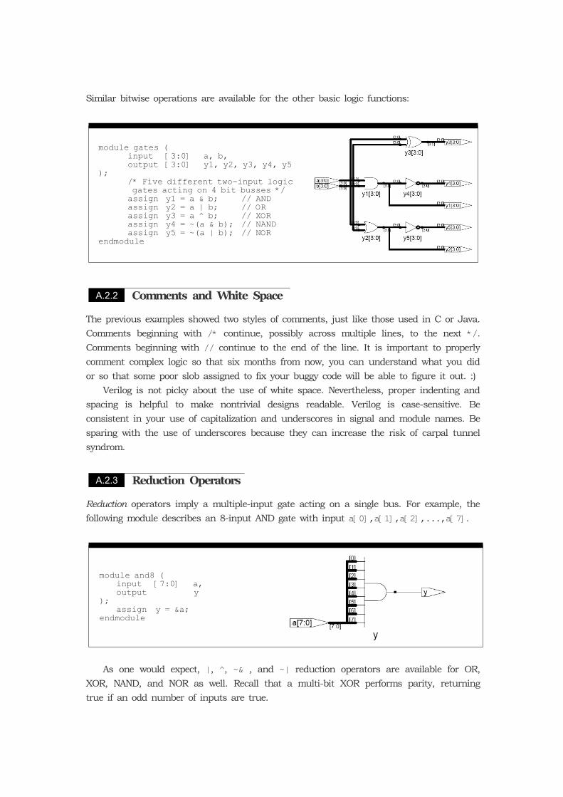
Similar bitwise operations are available for the other basic logic functions:
module gates (input [3:0] a, b,output [3:0] y1, y2, y3, y4, y5
);/* Five different two-input logic
gates acting on 4 bit busses */assign y1 = a & b; // ANDassign y2 = a | b; // ORassign y3 = a ̂ b; // XORassign y4 = ~(a & b); // NANDassign y5 = ~(a | b); // NOR
endmodule
The previous examples showed two styles of comments, just like those used in C or Java. Comments beginning with /* continue, possibly across multiple lines, to the next */. Comments beginning with // continue to the end of the line. It is important to properly comment complex logic so that six months from now, you can understand what you did or so that some poor slob assigned to fix your buggy code will be able to figure it out. :) Verilog is not picky about the use of white space. Nevertheless, proper indenting and spacing is helpful to make nontrivial designs readable. Verilog is case-sensitive. Be consistent in your use of capitalization and underscores in signal and module names. Be sparing with the use of underscores because they can increase the risk of carpal tunnel syndrom.
Reduction operators imply a multiple-input gate acting on a single bus. For example, the following module describes an 8-input AND gate with input a[0],a[1],a[2],...,a[7].
module and8 ( input [7:0] a, output y); assign y = &a;endmodule
As one would expect, |, ,̂ ~& , and ~| reduction operators are available for OR, XOR, NAND, and NOR as well. Recall that a multi-bit XOR performs parity, returning true if an odd number of inputs are true.
A.3 Basic Constructs
A.2.4 Other Operators
A.3.1 Internal Signals
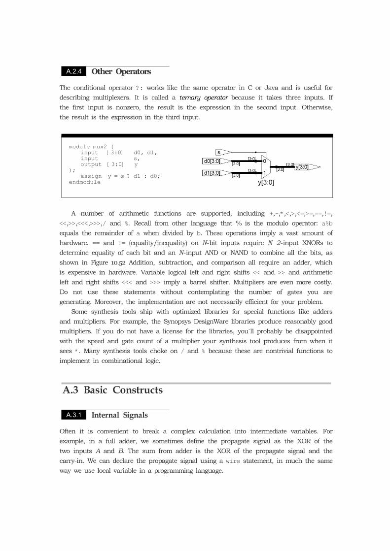
The conditional operator ?: works like the same operator in C or Java and is useful for describing multiplexers. It is called a ternary operator because it takes three inputs. If the first input is nonzero, the result is the expression in the second input. Otherwise, the result is the expression in the third input.
module mux2 ( input [3:0] d0, d1, input s, output [3:0] y); assign y = s ? d1 : d0;endmodule
A number of arithmetic functions are supported, including +,-,*,<,>,<=,>=,==,!=, <<,>>,<<<,>>>,/ and %. Recall from other language that % is the modulo operator: a%b equals the remainder of a when divided by b. These operations imply a vast amount of hardware. == and != (equality/inequality) on N-bit inputs require N 2-input XNORs to determine equality of each bit and an N-input AND or NAND to combine all the bits, as shown in Figure 10.52 Addition, subtraction, and comparison all require an adder, which is expensive in hardware. Variable logical left and right shifts << and >> and arithmetic left and right shifts <<< and >>> imply a barrel shifter. Multipliers are even more costly. Do not use these statements without contemplating the number of gates you are generating. Moreover, the implementation are not necessarily efficient for your problem. Some synthesis tools ship with optimized libraries for special functions like adders and multipliers. For example, the Synopsys DesignWare libraries produce reasonably good multipliers. If you do not have a license for the libraries, you`ll probably be disappointed with the speed and gate count of a multiplier your synthesis tool produces from when it sees *. Many synthesis tools choke on / and % because these are nontrivial functions to implement in combinational logic.
Often it is convenient to break a complex calculation into intermediate variables. For example, in a full adder, we sometimes define the propagate signal as the XOR of the two inputs A and B. The sum from adder is the XOR of the propagate signal and the carry-in. We can declare the propagate signal using a wire statement, in much the same way we use local variable in a programming language.
A.3.2 Precedence
module fulladder ( input a, b, cin, output s, cout);
wire prop;
assign prop = a ̂ b; assign s = prop ̂ cin; assign cout = (a & b) | (cin & (a | b));endmodule
Technically, it is not necessary to declare single-bit wires. However, it is necessary to declare multi-bit busses and is good practice to declare all signals. Some Verilog simulation and synthesis tools give errors that are difficult to decipher when a wire is not declared.
Notice that we fully parenthesized the cout computation. We could take advantage of operator precedence to use fewer parentheses:
assign cout = a&b | cin&(a|b);
The operator precedence from highest to lowest is much as you would expect in other languages, as shown in Table A.1. AND has precedence over OR.
Table A.1 Operator Precedence Symbol Meaning Precedence~ NOT Highest*, /, * MUL, DIV, MODULO+, - PLUS, MINUS<<, >> Logical Left/Right Shift<<<, >>> Arithmetic Left/Right Shift<, <=, >, >= Relative Comparison==, != Equality Comparison&, ~& AND, NAND^, ~^ XOR, XNOR|, ~| OR, NOR?: Conditional Lowest
A.3.3 Constants
A.3.4 Hierarchy
Constants can be specified in binary, octal, decimal, or hexadecimal. Table A.2 gives examples.
Table A.2 ConstantsNumber # Bits Base Decimal Equivalent Stored3'b101 3 Binary 5 101'b11 unsized Binary 3 000000..000118'b11 8 Binary 3 000000118'b1010_1011 8 Binary 171 101010113'd6 3 Decimal 6 1106'o42 6 Octal 34 1000108'hAB 8 Hexadecimal 171 1010101142 unsized Decimal 42 0000....00101010
It is good practice to specify the length of the number in bits, even though the second row shows that this is not strictly necessary. If you don't specify the length, one day you may be surprised when Verilog assumes the constant has additional leading 0’s that you didn't intend. Underscores in numbers are ignored and can be helpful in breaking long numbers into more readable chunks. If the base is omitted, the number is assumed to be decimal.
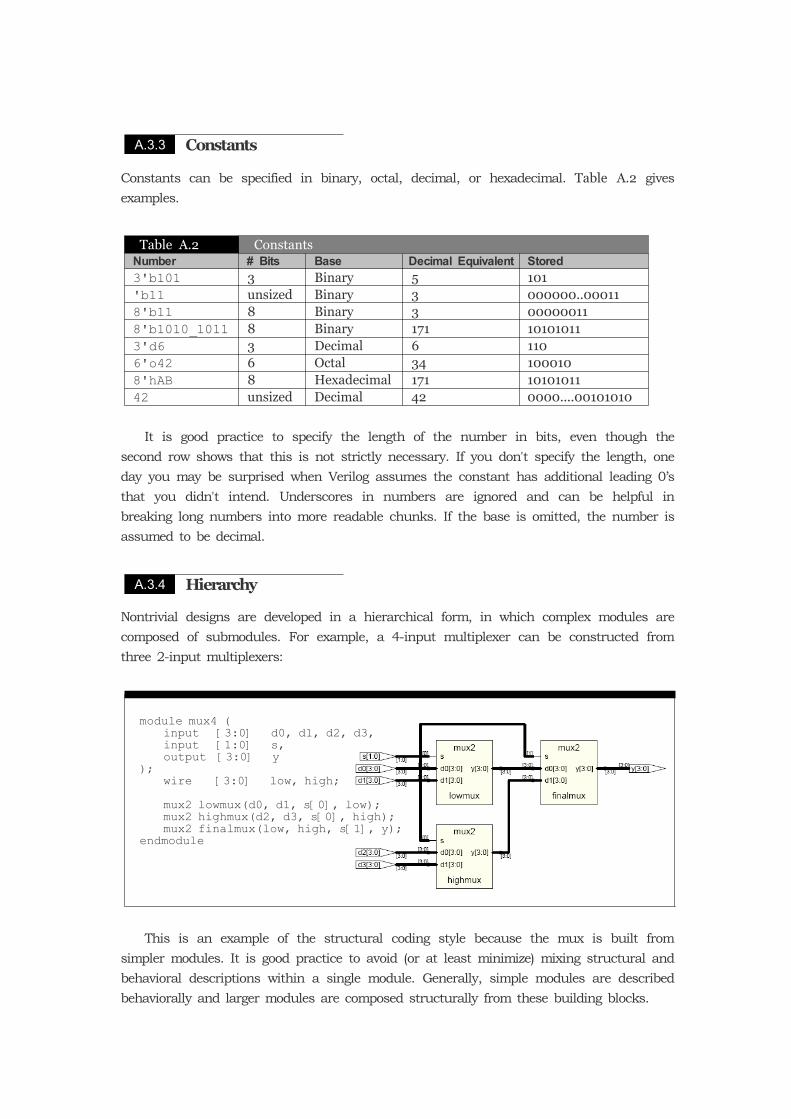
Nontrivial designs are developed in a hierarchical form, in which complex modules are composed of submodules. For example, a 4-input multiplexer can be constructed from three 2-input multiplexers:
module mux4 ( input [3:0] d0, d1, d2, d3, input [1:0] s, output [3:0] y); wire [3:0] low, high;
mux2 lowmux(d0, d1, s[0], low); mux2 highmux(d2, d3, s[0], high); mux2 finalmux(low, high, s[1], y);endmodule
This is an example of the structural coding style because the mux is built from simpler modules. It is good practice to avoid (or at least minimize) mixing structural and behavioral descriptions within a single module. Generally, simple modules are described behaviorally and larger modules are composed structurally from these building blocks.
A.3.5 Tristates
A.3.6 Bit Swizzling
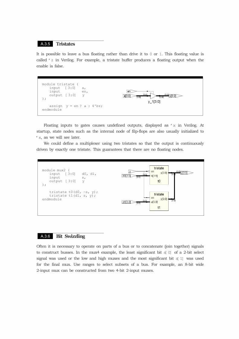
It is possible to leave a bus floating rather than drive it to 0 or 1. This floating value is called ’z in Verilog. For example, a tristate buffer produces a floating output when the enable is false.
module tristate ( input [3:0] a, input en, output [3:0] y);
assign y = en ? a : 4'bz;endmodule
Floating inputs to gates causes undefined outputs, displayed as ’x in Verilog. At startup, state nodes such as the internal node of filp-flops are also usually initialized to ’x, as we will see later. We could define a multiplexer using two tristates so that the output is continuously driven by exactly one tristate. This guarantees that there are no floating nodes.
module mux2 ( input [3:0] d0, d1, input s, output [3:0] y);
tristate t0(d0, ~s, y); tristate t1(d1, s, y);endmodule
Often it is necessary to operate on parts of a bus or to concatenate (join together) signals to construct busses. In the mux4 example, the least significant bit s[0] of a 2-bit select signal was used or the low and high muxes and the most significant bit s[1] was used for the final mux. Use ranges to select subsets of a bus. For example, an 8-bit wide 2-input mux can be constructed from two 4-bit 2-input muxes.
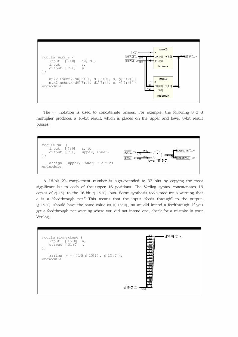
module mu1 ( input [7:0] a, b, output [7:0] upper, lower,);
assign {upper, lower} = a * b;endmodule
module mux2_8 ( input [7:0] d0, d1, input s, output [7:0] y);
mux2 lsbmux(d0[3:0], d1[3:0], s, y[3:0]); mux2 msbmux(d0[7:4], d1[7:4], s, y[7:4]);endmodule
The {} notation is used to concatenate busses. For example, the following 8 x 8 multiplier produces a 16-bit result, which is placed on the upper and lower 8-bit result busses.
A 16-bit 2’s complement number is sign-extended to 32 bits by copying the most significant bit to each of the upper 16 positions. The Verilog syntax concatenates 16 copies of a[15] to the 16-bit a[15:0] bus. Some synthesis tools produce a warning that a is a “feedthrough net.” This means that the input “feeds through” to the output. y[15:0] should have the same value as a[15:0], so we did intend a feedthrough. If you get a feedthrough net warning where you did not intend one, check for a mistake in your Verilog.
module signextend ( input [15:0] a, output [31:0] y);
assign y = {{16{a[15]}}, a[15:0]};endmodule
A.4 Behavioral Modeling with Always Blocks
A.3.7 Delays
A.4.1 Registers
The next statement generates a silly combination of two busses. Don’t confuse the 3-bit binary constant 3’b101 with bus b. Note that it was important to specify the length of 3 bits in the constant; otherwise many additional 0’s might have appeared in the middle of y.
assign y = {a[2:1], {3{b[0]}}, a[0], 3'b101, b[1:3]};
This produces
y = a[2] a[1] b[0] b[0] b[0] b[0] 1 0 1 b[1] b[2] b[3]
The delay of a statement can be specified in arbitrary units. For example, the following code defines an inverter with a 42-unit propagation delay. Delays have no impact on synthesis, but can be helpful while debugging simulation waveforms because they make cause and effect more apparent.
assign #42 y = -a;
Assign statements are reevaluated every time any term on the right side changes. Therefore, they must describe combinational logic. Always blocks are reevaluated only when signals in the header (called a sensitivity list) change. Depending on the form, always blocks can imply either sequential or combinational circuits.
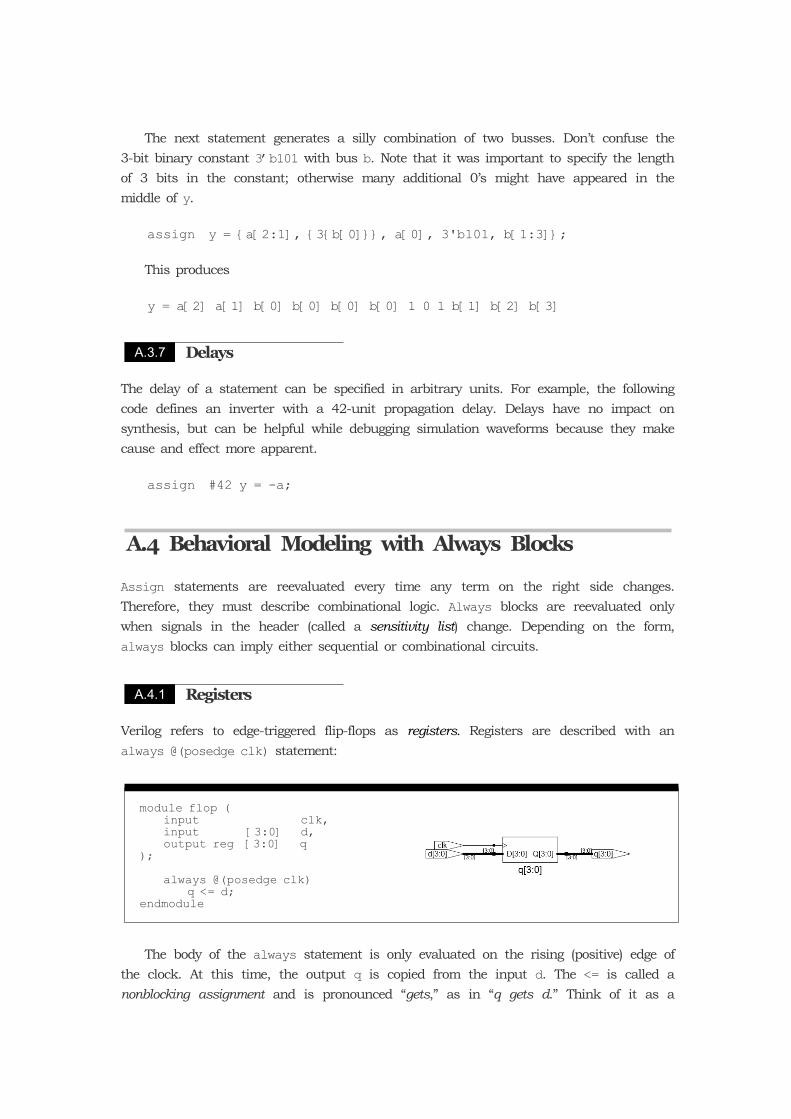
Verilog refers to edge-triggered flip-flops as registers. Registers are described with an always @(posedge clk) statement:
module flop ( input clk, input [3:0] d, output reg [3:0] q);
always @(posedge clk) q <= d;endmodule
The body of the always statement is only evaluated on the rising (positive) edge of the clock. At this time, the output q is copied from the input d. The <= is called a nonblocking assignment and is pronounced “gets,” as in “q gets d.” Think of it as a
regular equals sign for now; we’ll return to the more subtle points in Section A.4.6. Notice that <= is used instead of assign inside the always block. All the signals on the left side of assignments in always block must be declared as reg. This is a confusing point for new Verilog users. In this circuit, q is also the output. Declaring a signal as reg does not mean the signal is actually a register! All it means is that it appears on the left side in an always block. We will see examples of combinational signals later that are declared reg, but that have no flip-flops. At startup, the q output is initialized to ’x. Generally, it is good practice to use resettable registers so that on power-up your system in a known state. The reset can be either asynchronous or synchronous, as discussed in Section 7.3.4. Asynchronous resets occur immediately. Synchronous resets only change the output on the rising edge of the clock.
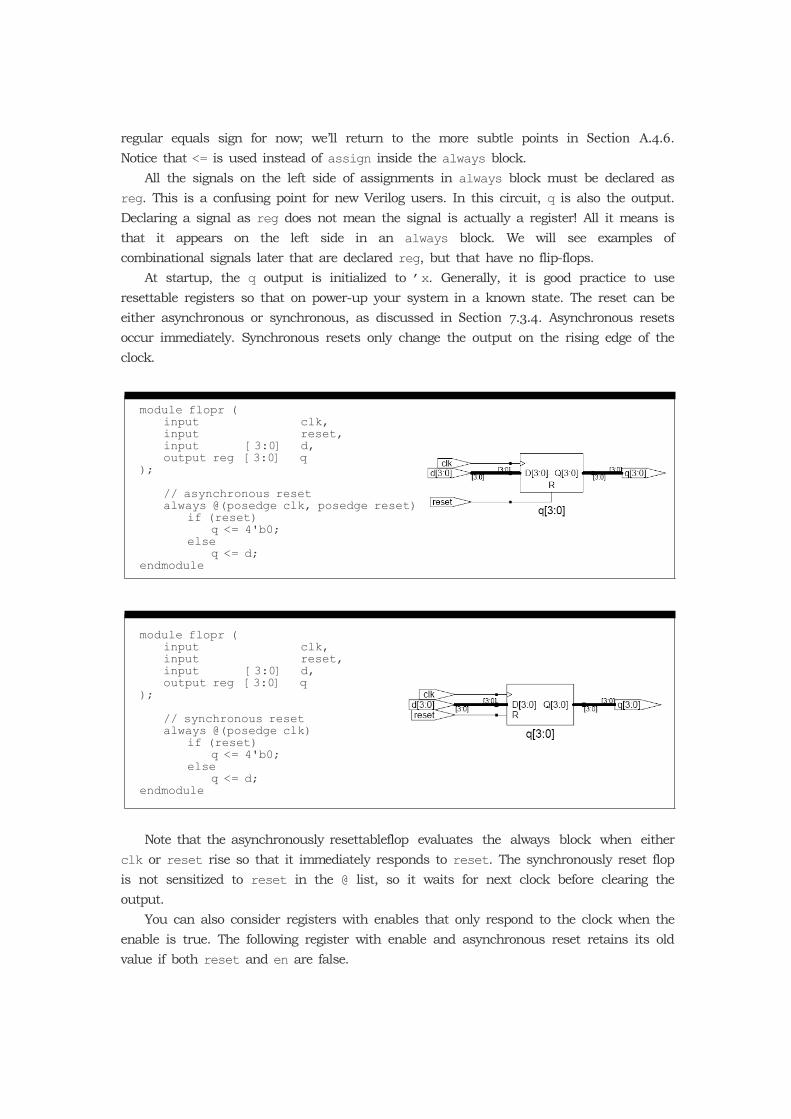
module flopr ( input clk, input reset, input [3:0] d, output reg [3:0] q);
// asynchronous reset always @(posedge clk, posedge reset) if (reset) q <= 4'b0; else q <= d;endmodule
module flopr ( input clk, input reset, input [3:0] d, output reg [3:0] q);
// synchronous reset always @(posedge clk) if (reset) q <= 4'b0; else q <= d;endmodule
Note that the asynchronously resettableflop evaluates the always block when either clk or reset rise so that it immediately responds to reset. The synchronously reset flop is not sensitized to reset in the @ list, so it waits for next clock before clearing the output. You can also consider registers with enables that only respond to the clock when the enable is true. The following register with enable and asynchronous reset retains its old value if both reset and en are false.
A.4.2 Latches
A.4.3 Counters
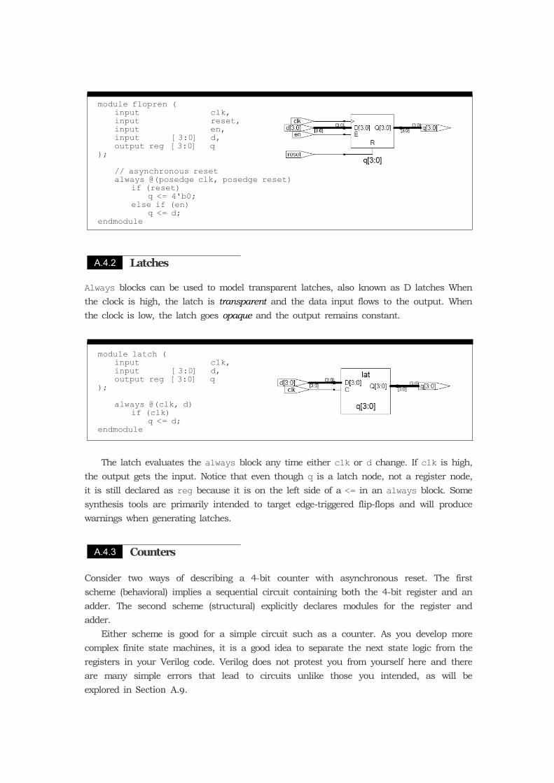
module flopren ( input clk, input reset, input en, input [3:0] d, output reg [3:0] q);
// asynchronous reset always @(posedge clk, posedge reset) if (reset) q <= 4'b0; else if (en) q <= d;endmodule
Always blocks can be used to model transparent latches, also known as D latches When the clock is high, the latch is transparent and the data input flows to the output. When the clock is low, the latch goes opaque and the output remains constant.
module latch ( input clk, input [3:0] d, output reg [3:0] q);
always @(clk, d) if (clk) q <= d;endmodule
The latch evaluates the always block any time either clk or d change. If clk is high, the output gets the input. Notice that even though q is a latch node, not a register node, it is still declared as reg because it is on the left side of a <= in an always block. Some synthesis tools are primarily intended to target edge-triggered flip-flops and will produce warnings when generating latches.
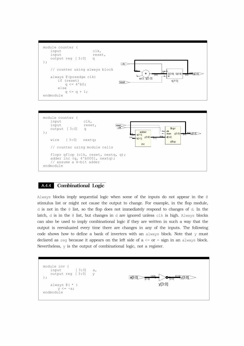
Consider two ways of describing a 4-bit counter with asynchronous reset. The first scheme (behavioral) implies a sequential circuit containing both the 4-bit register and an adder. The second scheme (structural) explicitly declares modules for the register and adder. Either scheme is good for a simple circuit such as a counter. As you develop more complex finite state machines, it is a good idea to separate the next state logic from the registers in your Verilog code. Verilog does not protest you from yourself here and there are many simple errors that lead to circuits unlike those you intended, as will be explored in Section A.9.
A.4.4 Combinational Logic
module counter ( input clk, input reset, output reg [3:0] q);
// counter using always block
always @(posedge clk) if (reset) q <= 4'b0; else q <= q + 1;endmodule
module counter ( input clk, input reset, output [3:0] q);
wire [3:0] nextq;
// counter using module calls
flopr qflop (clk, reset, nextq, q); adder inc (q, 4'b0001, nextq); // assume a 4-bit adderendmodule
Always blocks imply sequential logic when some of the inputs do not appear in the @ stimulus list or might not cause the output to change. For example, in the flop module, d is not in the @ list, so the flop does not immediately respond to changes of d. In the latch, d is in the @ list, but changes in d are ignored unless clk is high. Always blocks can also be used to imply combinational logic if they are written in such a way that the output is reevaluated every time there are changes in any of the inputs. The following code shows how to define a bank of inverters with an always block. Note that y must declared as reg because it appears on the left side of a <= or = sign in an always block. Nevertheless, y is the output of combinational logic, not a register.
module inv ( input [3:0] a, output reg [3:0] y);
always @( * ) y <= ~a;endmodule
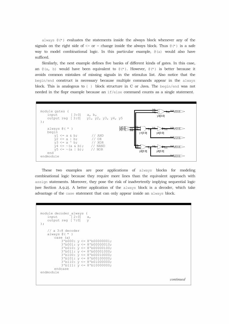
always @(*) evaluates the statements inside the always block whenever any of the signals on the right side of <= or = change inside the always block. Thus @(*) is a safe way to model combinational logic. In this particular example, @(a) would also have sufficed. Similarly, the next example defines five banks of different kinds of gates. In this case, an @(a, b) would have been equivalent to @(*). However, @(*) is better because it avoids common mistakes of missing signals in the stimulus list. Also notice that the begin/end construct is necessary because multiple commands appear in the always block. This is analogous to { } block structure in C or Java. The begin/end was not needed in the flopr example because an if/else command counts as a single statement.
module gates ( input [3:0] a, b, output reg [3:0] y1, y2, y3, y4, y5);
always @( * ) begin y1 <= a & b; // AND y2 <= a | b; // OR y3 <= a ̂ b; // XOR y4 <= ~(a & b); // NAND y5 <= ~(a | b); // NOR endendmodule
These two examples are poor applications of always blocks for modeling combinational logic because they require more lines than the equivalent approach with assign statements. Moreover, they pose the risk of inadvertently implying sequential logic (see Section A.9.2). A better application of the always block is a decoder, which take advantage of the case statement that can only appear inside an always block.
module decoder_always ( input [2:0] a, output reg [7:0] y);
// a 3:8 decoder always @( * ) case (a) 3'b000: y <= 8'b00000001; 3'b001: y <= 8'b00000010; 3'b010: y <= 8'b00000100; 3'b011: y <= 8'b00001000; 3'b100: y <= 8'b00010000; 3'b101: y <= 8'b00100000; 3'b110: y <= 8'b01000000; 3'b111: y <= 8'b10000000; endcaseendmodule
continued
Using the case statement is probably clearer than using Boolean equations in as assign statement:
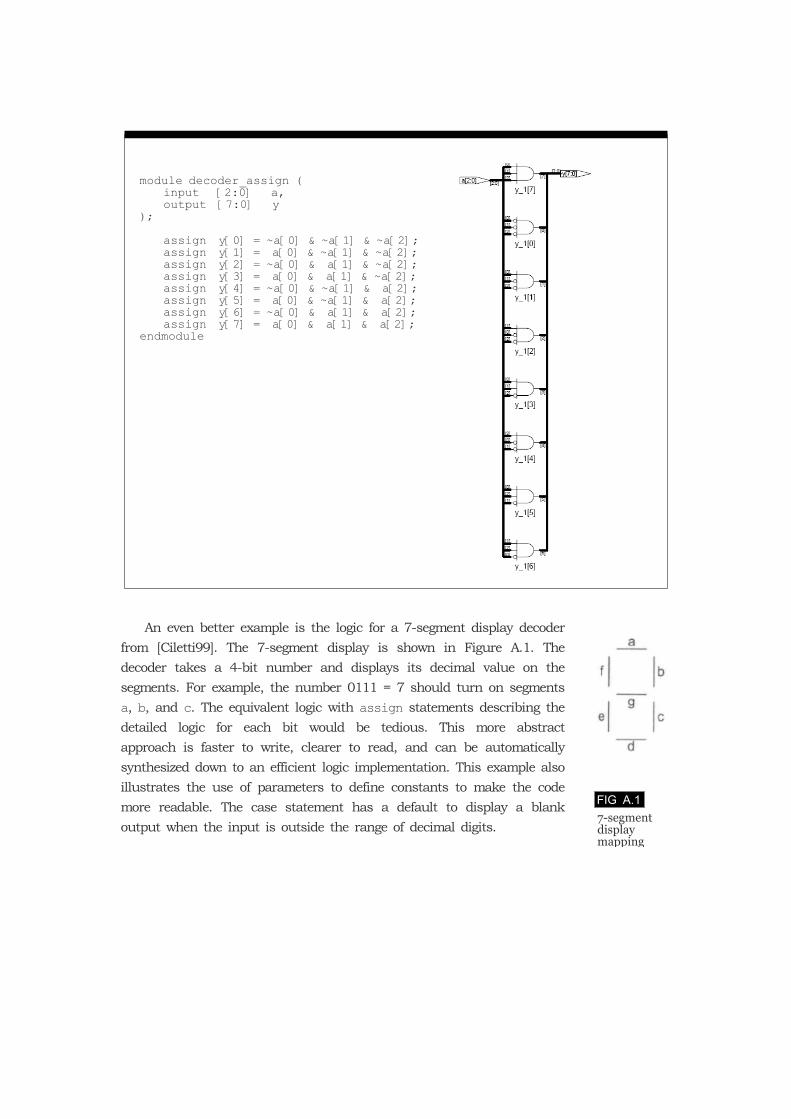
FIG A.17-segmentdisplaymapping
module decoder_assign ( input [2:0] a, output [7:0] y);
assign y[0] = ~a[0] & ~a[1] & ~a[2]; assign y[1] = a[0] & ~a[1] & ~a[2]; assign y[2] = ~a[0] & a[1] & ~a[2]; assign y[3] = a[0] & a[1] & ~a[2]; assign y[4] = ~a[0] & ~a[1] & a[2]; assign y[5] = a[0] & ~a[1] & a[2]; assign y[6] = ~a[0] & a[1] & a[2]; assign y[7] = a[0] & a[1] & a[2];endmodule
An even better example is the logic for a 7-segment display decoder from [Ciletti99]. The 7-segment display is shown in Figure A.1. The decoder takes a 4-bit number and displays its decimal value on the segments. For example, the number 0111 = 7 should turn on segments a, b, and c. The equivalent logic with assign statements describing the detailed logic for each bit would be tedious. This more abstract approach is faster to write, clearer to read, and can be automatically synthesized down to an efficient logic implementation. This example also illustrates the use of parameters to define constants to make the code more readable. The case statement has a default to display a blank output when the input is outside the range of decimal digits.
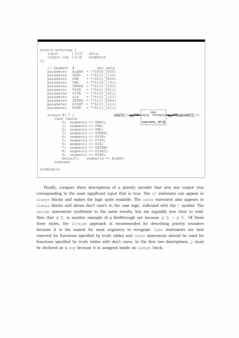
module sevenseg ( input [3:0] data, output reg [6:0] segments);
// Segment # abc_defg parameter BLANK = 7'b000_0000; parameter ZERO = 7'b111_1110; parameter ONE = 7'b011_0000; parameter TWO = 7'b110_1101; parameter THREE = 7'b111_1001; parameter FOUR = 7'b011_0011; parameter FIVE = 7'b101_1011; parameter SIX = 7'b101_1111; parameter SEVEN = 7'b111_0000; parameter EIGHT = 7'b111_1111; parameter NINE = 7'b111_1011;
always @( * ) case (data) 0: segments <= ZERO; 1: segments <= ONE; 2: segments <= TWO; 3: segments <= THREE; 4: segments <= FOUR; 5: segments <= FIVE; 6: segments <= SIX; 7: segments <= SEVEN; 8: segments <= EIGHT; 9: segments <= NINE; default: segments <= BLANK; endcase
endmodule
Finally, compare three descriptions of a priority encoder that sets one output true corresponding to the most significant input that is true. The if statement can appear in always blocks and makes the logic quite readable. The casez statement also appears in always blocks and allows don’t care’s in the case logic, indicated with the ? symbol. The assign statements synthesize to the same results, but are arguably less clear to read. Note that a[3] is another example of a feedthrough net because y[3] = a[3]. Of these three styles, the if/else approach is recommended for describing priority encoders because it is the easiest for most engineers to recognize. Case statements are best reserved for functions specified by truth tables and casez statements should be used for functions specified by truth tables with don’t cares. In the first two descriptions, y must be declared as a reg because it is assigned inside an always block.
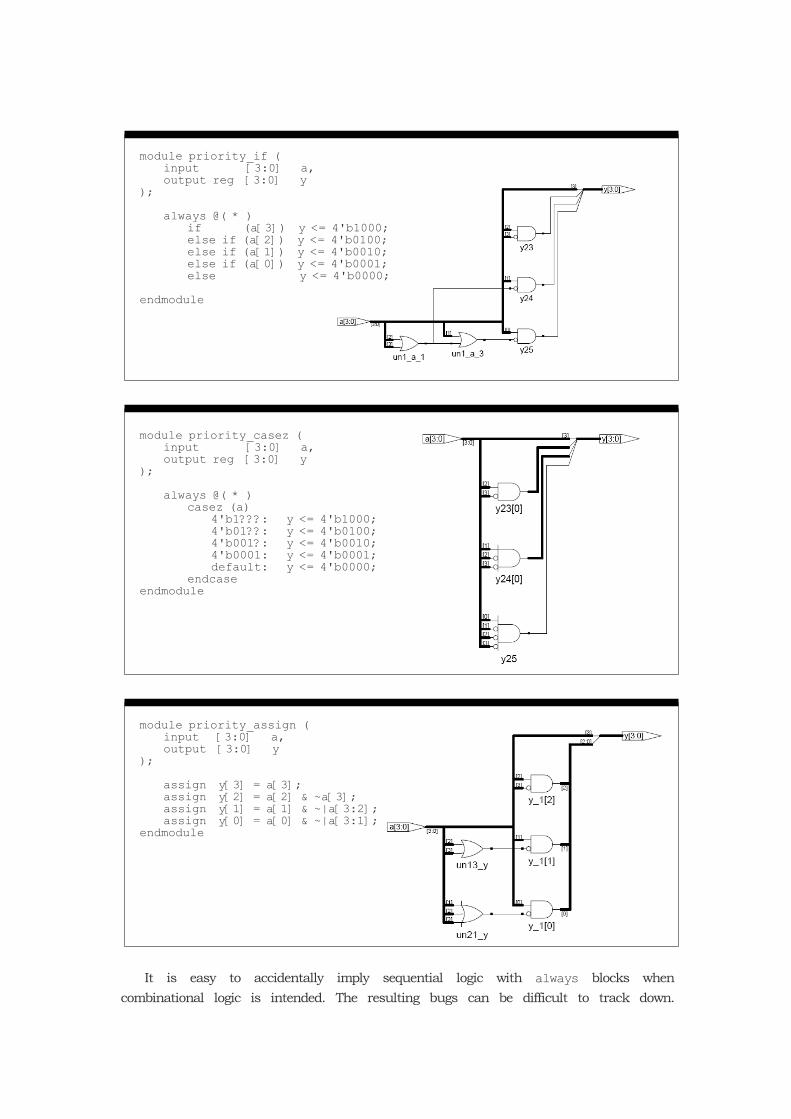
module priority_if ( input [3:0] a, output reg [3:0] y);
always @( * ) if (a[3]) y <= 4'b1000; else if (a[2]) y <= 4'b0100; else if (a[1]) y <= 4'b0010; else if (a[0]) y <= 4'b0001; else y <= 4'b0000;
endmodule
module priority_casez ( input [3:0] a, output reg [3:0] y);
always @( * ) casez (a) 4'b1???: y <= 4'b1000; 4'b01??: y <= 4'b0100; 4'b001?: y <= 4'b0010; 4'b0001: y <= 4'b0001; default: y <= 4'b0000; endcaseendmodule
module priority_assign ( input [3:0] a, output [3:0] y);
assign y[3] = a[3]; assign y[2] = a[2] & ~a[3]; assign y[1] = a[1] & ~|a[3:2]; assign y[0] = a[0] & ~|a[3:1];endmodule
It is easy to accidentally imply sequential logic with always blocks when combinational logic is intended. The resulting bugs can be difficult to track down.
A.4.5 Memories
A.4.6 Blocking and Nonblocking Assignment
Therefore, to imply combinational logic, it is safer to use assign statements than always blocks. Nevertheless, the convenience of constructs such as if or case that must appear in always blocks justifies the modeling style as long as you thoroughly understand what you are doing.
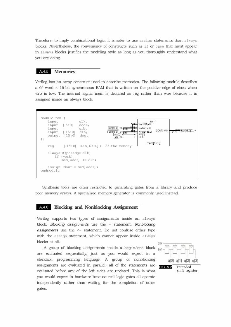
Verilog has an array construct used to describe memories. The following module describes a 64-word × 16-bit synchronous RAM that is written on the positive edge of clock when wrb is low. The internal signal mem is declared as reg rather than wire because it is assigned inside an always block.
module ram ( input clk, input [5:0] addr, input wrb, input [15:0] din, output [15:0] dout);
reg [15:0] mem[63:0]; // the memory
always @(posedge clk) if (~wrb) mem[addr] <= din;
assign dout = mem[addr];endmodule
Synthesis tools are often restricted to generating gates from a library and produce poor memory arrays. A specialized memory generator is commonly used instead.
Verilog supports two types of assignments inside an always block. Blocking assignments use the = statement. Nonblocking assignments use the <= statement. Do not confuse either type with the assign statement, which cannot appear inside always blocks at all. A group of blocking assignments inside a begin/end block are evaluated sequentially, just as you would expect in a standard programming language. A group of nonblocking assignments are evaluated in parallel; all of the statements are evaluated before any of the left sides are updated. This is what you would expect in hardware because real logic gates all operate independently rather than waiting for the completion of other gates.
FIG A.2 Intendedshift register
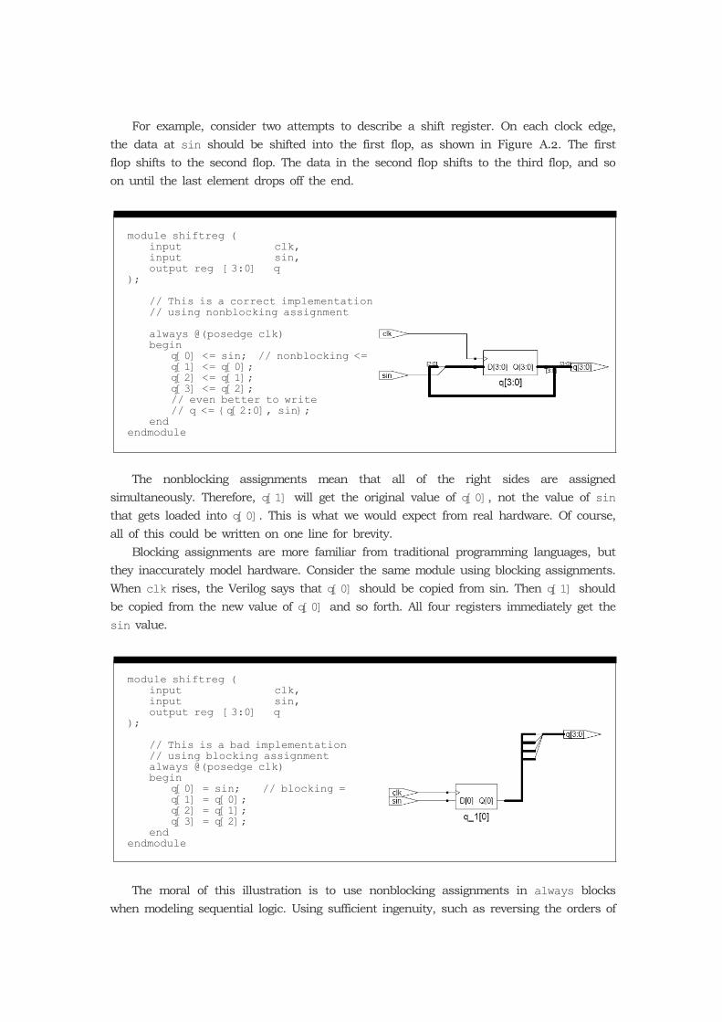
For example, consider two attempts to describe a shift register. On each clock edge, the data at sin should be shifted into the first flop, as shown in Figure A.2. The first flop shifts to the second flop. The data in the second flop shifts to the third flop, and so on until the last element drops off the end.
module shiftreg ( input clk, input sin, output reg [3:0] q);
// This is a correct implementation // using nonblocking assignment
always @(posedge clk) begin q[0] <= sin; // nonblocking <= q[1] <= q[0]; q[2] <= q[1]; q[3] <= q[2]; // even better to write // q <= {q[2:0], sin}; endendmodule
The nonblocking assignments mean that all of the right sides are assigned simultaneously. Therefore, q[1] will get the original value of q[0], not the value of sin that gets loaded into q[0]. This is what we would expect from real hardware. Of course, all of this could be written on one line for brevity. Blocking assignments are more familiar from traditional programming languages, but they inaccurately model hardware. Consider the same module using blocking assignments. When clk rises, the Verilog says that q[0] should be copied from sin. Then q[1] should be copied from the new value of q[0] and so forth. All four registers immediately get the sin value.
module shiftreg ( input clk, input sin, output reg [3:0] q);
// This is a bad implementation // using blocking assignment always @(posedge clk) begin q[0] = sin; // blocking = q[1] = q[0]; q[2] = q[1]; q[3] = q[2]; endendmodule
The moral of this illustration is to use nonblocking assignments in always blocks when modeling sequential logic. Using sufficient ingenuity, such as reversing the orders of
A.5 Finite State Machines
FIG A.4 Divide-by-3 counterstate transition diagram
the four commands, you could make blocking assignments work correctly, but they offer no advantages and harbor great risks. Finally, note that each always block implies a separate block of logic. Therefore, a given reg can be assigned in only one always block. Otherwise, two prices of hardware with shorted outputs will be implied.
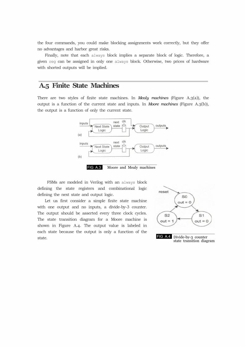
There are two styles of finite state machines. In Mealy machines (Figure A.3(a)), the output is a function of the current state and inputs. In Moore machines (Figure A.3(b)), the output is a function of only the current state.
FIG A.3 Moore and Mealy machines
FSMs are modeled in Verilog with an always block defining the state registers and combinational logic defining the next state and output logic. Let us first consider a simple finite state machine with one output and no inputs, a divide-by-3 counter. The output should be asserted every three clock cycles. The state transition diagram for a Moore machine is shown in Figure A.4. The output value is labeled in each state because the output is only a function of the state.
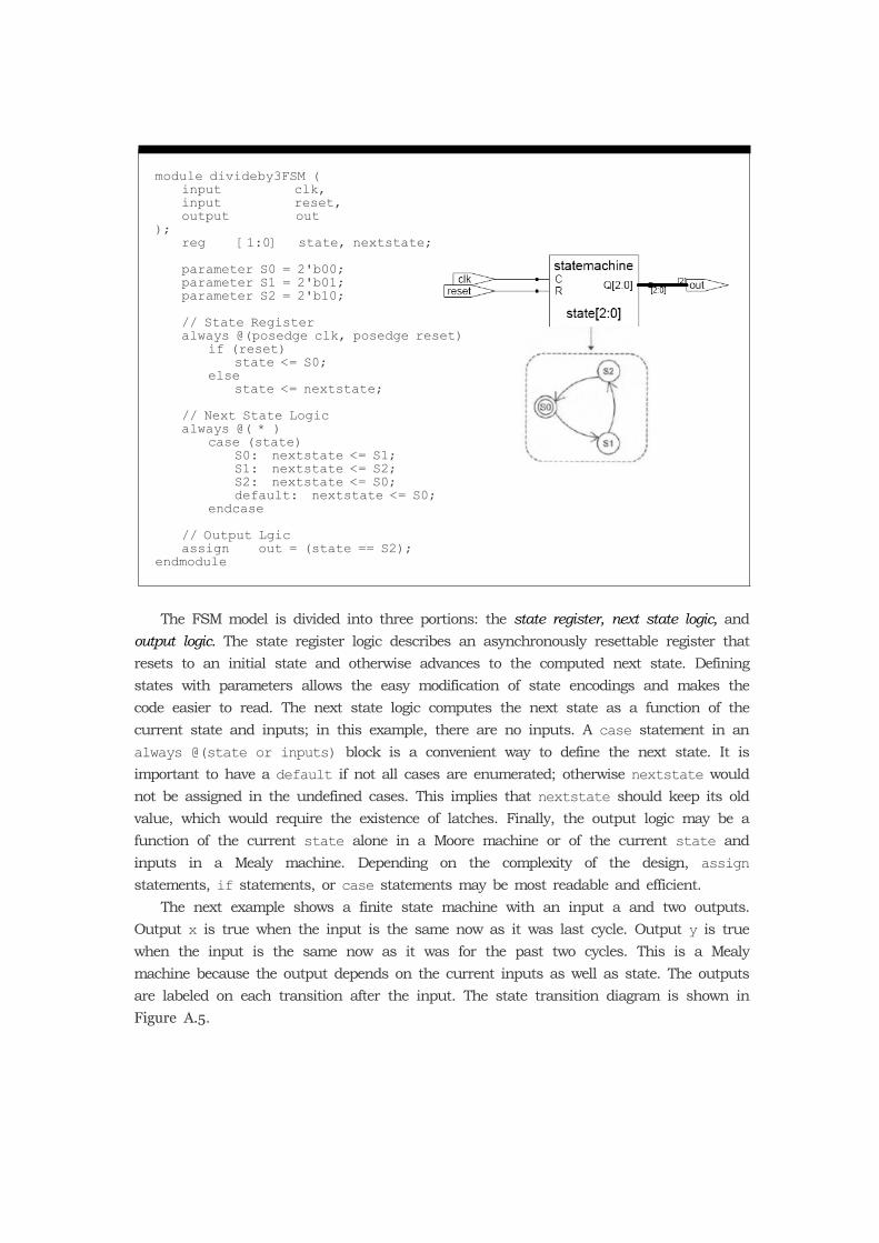
module divideby3FSM ( input clk, input reset, output out); reg [1:0] state, nextstate;
parameter S0 = 2'b00; parameter S1 = 2'b01; parameter S2 = 2'b10;
// State Register always @(posedge clk, posedge reset) if (reset) state <= S0; else state <= nextstate;
// Next State Logic always @( * ) case (state) S0: nextstate <= S1; S1: nextstate <= S2; S2: nextstate <= S0; default: nextstate <= S0; endcase
// Output Lgic assign out = (state == S2);endmodule
The FSM model is divided into three portions: the state register, next state logic, and output logic. The state register logic describes an asynchronously resettable register that resets to an initial state and otherwise advances to the computed next state. Defining states with parameters allows the easy modification of state encodings and makes the code easier to read. The next state logic computes the next state as a function of the current state and inputs; in this example, there are no inputs. A case statement in an always @(state or inputs) block is a convenient way to define the next state. It is important to have a default if not all cases are enumerated; otherwise nextstate would not be assigned in the undefined cases. This implies that nextstate should keep its old value, which would require the existence of latches. Finally, the output logic may be a function of the current state alone in a Moore machine or of the current state and inputs in a Mealy machine. Depending on the complexity of the design, assign
statements, if statements, or case statements may be most readable and efficient. The next example shows a finite state machine with an input a and two outputs. Output x is true when the input is the same now as it was last cycle. Output y is true when the input is the same now as it was for the past two cycles. This is a Mealy machine because the output depends on the current inputs as well as state. The outputs are labeled on each transition after the input. The state transition diagram is shown in Figure A.5.
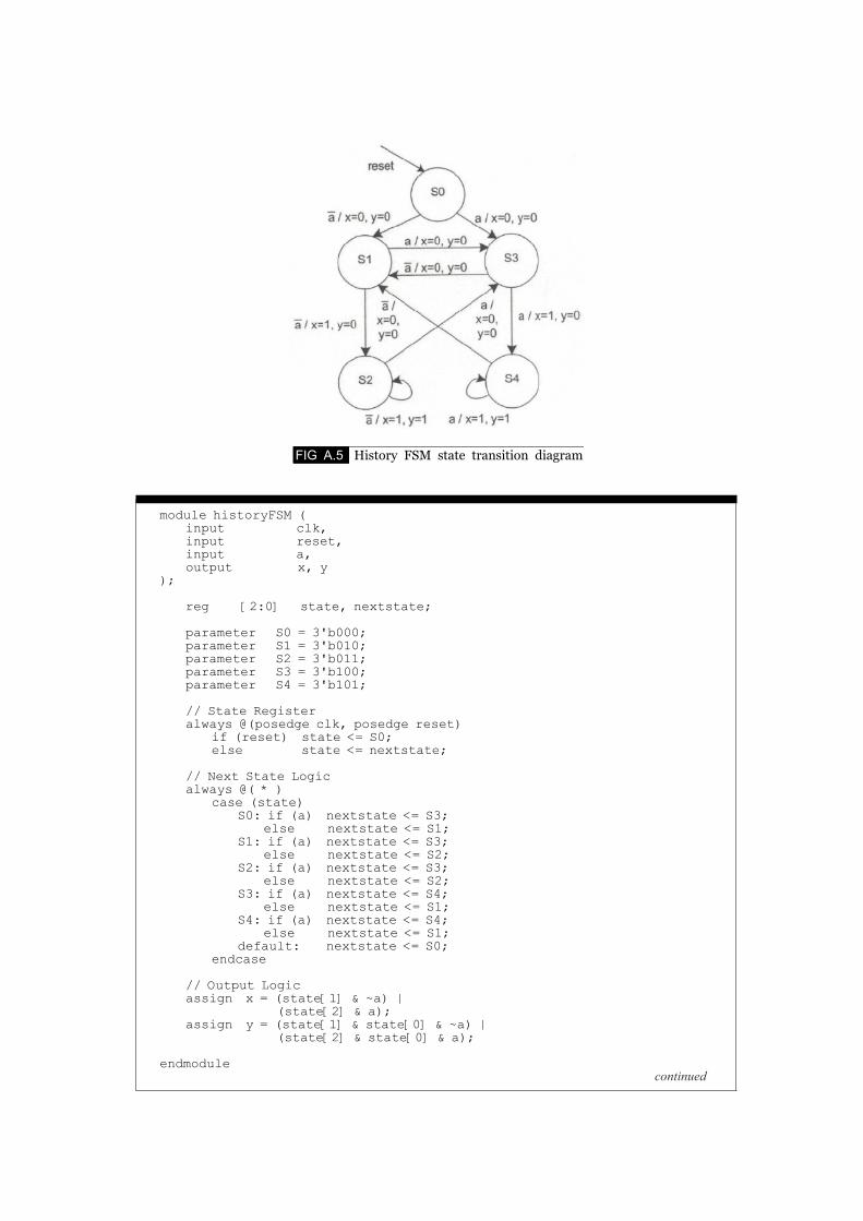
FIG A.5 History FSM state transition diagram
module historyFSM ( input clk, input reset, input a, output x, y);
reg [2:0] state, nextstate;
parameter S0 = 3'b000; parameter S1 = 3'b010; parameter S2 = 3'b011; parameter S3 = 3'b100; parameter S4 = 3'b101;
// State Register always @(posedge clk, posedge reset) if (reset) state <= S0; else state <= nextstate;
// Next State Logic always @( * ) case (state) S0: if (a) nextstate <= S3; else nextstate <= S1; S1: if (a) nextstate <= S3; else nextstate <= S2; S2: if (a) nextstate <= S3; else nextstate <= S2; S3: if (a) nextstate <= S4; else nextstate <= S1; S4: if (a) nextstate <= S4; else nextstate <= S1; default: nextstate <= S0; endcase
// Output Logic assign x = (state[1] & ~a) | (state[2] & a); assign y = (state[1] & state[0] & ~a) | (state[2] & state[0] & a);
endmodule continued
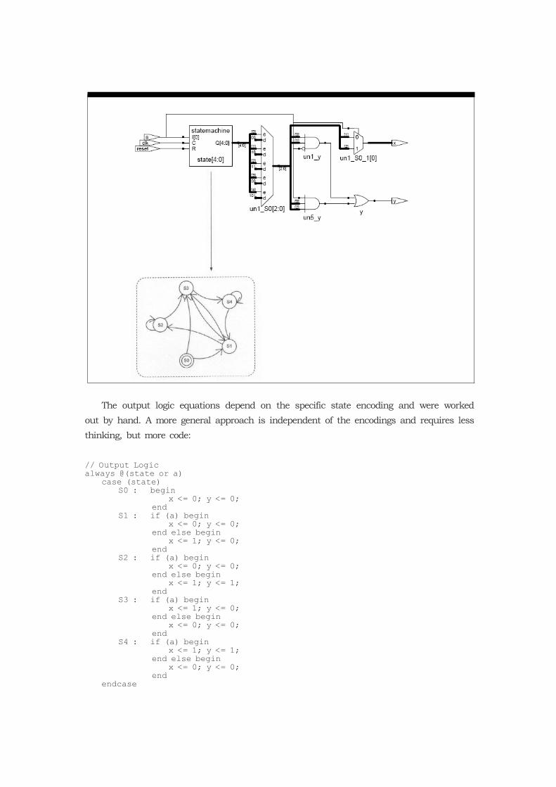
The output logic equations depend on the specific state encoding and were worked out by hand. A more general approach is independent of the encodings and requires less thinking, but more code:
// Output Logicalways @(state or a) case (state) S0 : begin x <= 0; y <= 0; end S1 : if (a) begin x <= 0; y <= 0; end else begin x <= 1; y <= 0; end S2 : if (a) begin x <= 0; y <= 0; end else begin x <= 1; y <= 1; end S3 : if (a) begin x <= 1; y <= 0; end else begin x <= 0; y <= 0; end S4 : if (a) begin x <= 1; y <= 1; end else begin x <= 0; y <= 0; end endcase
A.6 Parameterized Modules
You may be tempted so simplify the case statement. For example, case S4 could be reduced to:
// bad simplification of S4S4: if (a) begin y <= 1; end else begin x <= 0; y <= 0; end
The designer reasons that to get to static S4, we must have passed hrough state S3 with a high, setting x high. Therefore, the assignment of x is optimized out of S4 when a is high. This is incorrect reasoning. The modified approach implies sequential logic. Specifically, a latch is implied that holds the old value of x when x is not assigned. The latch holds its output under a peculiar set of circumstances; a and the state must be used to inadvertently imply. The moral of this example is that if any signal gets assigned in any branch of an if or case statement, it must be assigned in all branches lest a latch be implied.
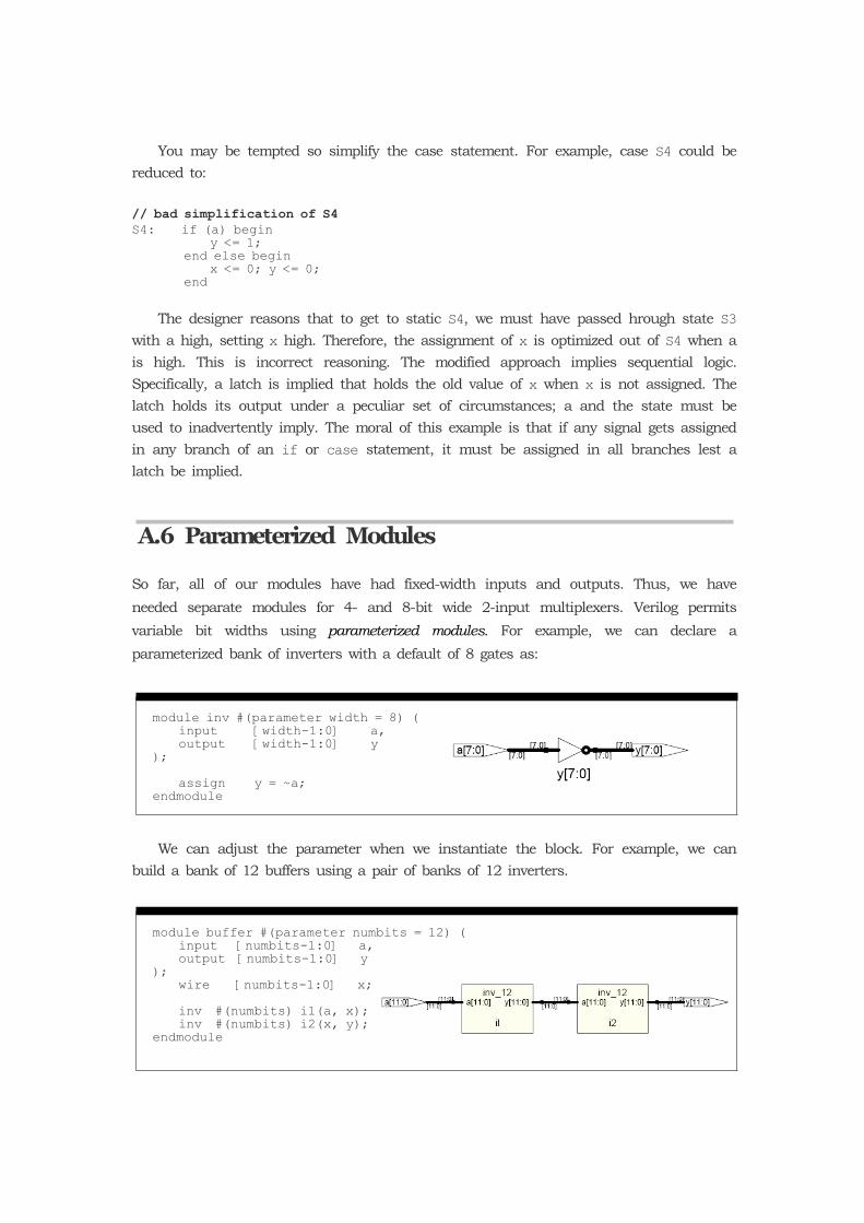
So far, all of our modules have had fixed-width inputs and outputs. Thus, we have needed separate modules for 4- and 8-bit wide 2-input multiplexers. Verilog permits variable bit widths using parameterized modules. For example, we can declare a parameterized bank of inverters with a default of 8 gates as:
module inv #(parameter width = 8) ( input [width-1:0] a, output [width-1:0] y);
assign y = ~a;endmodule
We can adjust the parameter when we instantiate the block. For example, we can build a bank of 12 buffers using a pair of banks of 12 inverters.
module buffer #(parameter numbits = 12) ( input [numbits-1:0] a, output [numbits-1:0] y); wire [numbits-1:0] x;
inv #(numbits) il(a, x); inv #(numbits) i2(x, y);endmodule
A.7 Structural Primitives
A.8 Test Benches
When coding at the structural level, primitives exist for basic logic gates and transistors. Examples for a full adder carry circuit (majority gate) were given in Section 1.8.4. Gate primitives include not, and, or, xor, nand, nor, and xnor. The output is declared first; multiple inputs may follow. For example, a 4-input AND gate may be given as
and g1(y, a, b, c, d);
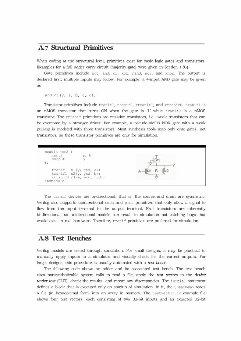
Transistor primitives include tranif1, tranif0, rtranif1, and rtranif0. tranif1 is an nMOS transistor that turns ON when the gate is ‘1’ while tranif0 is a pMOS transistor. The rtranif primitives are resistive transistors, i.e., weak transistors that can be overcome by a stronger driver. For example, a pseudo-nMOS NOR gate with a weak pull-up is modeled with three transistors. Most synthesis tools map only onto gates, not transistors, so these transistor primitives are only for simulation.
module nor2 ( input a, b, output y);
tranif1 n1(y, gnd, a); tranif1 n2(y, gnd, b); rtranif0 p1(y, vdd, gnd);endmodule
The tranif devices are bi-directional; that is, the source and drain are symmetric. Verilog also supports unidirectional nmos and pmos primitives that only allow a signal to flow from the input terminal to the output terminal. Real transistors are inherently bi-directional, so unidirectional models can result in simulation not catching bugs that would exist in real hardware. Therefore, tranif primitives are preferred for simulation.
Verilog models are tested through simulation. For small designs, it may be practical to manually apply inputs to a simulator and visually check for the correct outputs. For larger designs, this procedure is usually automated with a test bench. The following code shows an adder and its associated test bench. The test bench uses nonsynthesizable system calls to read a file, apply the test vectors to the device under test (DUT), check the results, and report any discrepancies. The initial statement defines a block that is executed only on startup of simulation. In it, the $readmemh reads a file (in hexadecimal form) into an array in memory. The testvector.tv example file shows four test vectors, each consisting of two 32-bit inputs and an expected 32-bit
output. As the array is much larger than the number of test vectors, the remaining entries are filled with x’s. The next always block defines a clock that repeats forever, being low for 50 units of time, then high for 50. On each positive edge of the clock, the next test vector is applied to the inputs and the expected output is saved. The actual output is sampled on the negative edge of the clock to permit some time for it to settle. It is not uncommon for bad logic to generate z and x values. The != and == comparison operations return x if either argument has z or x, so theyo are not reliable. The !== and === commands check for an exact match, including z or x values. If there is a mismatch, the $display command is used to print the discrepancy. Each time vectornum is incremented, the test bench checks to see if the test is complete. It terminates testing with the $finish command after 100 vectors have been applied or the test vector consists of x’s; for our testvector.tv file, it will end after the four vectors are applied.
module adder ( input [31:0] a, b, output [31:0] y;);
assign y = a + b;endmodule
module testbench(); reg [31:0] testvectors[1000:0]; reg clk; reg [10:0] vectornum, errors; reg [31:0] a, b, expectedy; wire [31:0] y;
// instantiate device under test adder dut(a, b, y);
// read the test vector file and initialize test initial begin $readmemh("testvectors.tv", testvectors); vectornum = 0; errors = 0; end
// generate a clock to sequence tests always begin clk = 0; #50; clk = 1; #50; end
// on each clock step, apply next test always @(posedge clk) begin a = testvectors[vectornum*3]; b = testvectors[vectornum*3 + 1]; expectedy = testvectors[vectornum*3 + 2]; end
// then check for correct results always @(negedge clk) begin vectornum = vectornum + 1; if (y !== expectedy) begin
A.9 Pitfalls
A.9.1 Verilog Style Guidelines
$display("Inputs were %h, %h", a, b); $display("Expected %h but actual %h", expectedy, y); errors = errors + 1; end end
// halt at the end of file always @(vectornum) begin if (vectornum == 100 || testvectors[vectornum*3] === 32'bx) begin $display("Completed %d tests with %d errors.", vectornum, errors); $finish; end endendmodule
testvectors.tv file:000000000000000000000000
000000010000000000000001
ffffffff0000000300000002
12345678123456782468acf0
This section includes a set of style guidelines and examples of a number of bad circuits produced by common Verilog coding errors. The examples include the warnings given by Synopsys Design Compiler and Synplify Pro synthesis tools.
1. Use only nonblocking assignments inside always blocks.
2. Define your combinational logic using assign statements when practical. Only use always blocks to define combinational logic if constructs like if or case make your logic much clearer or more compact.
3. When modeling combinational logic with an always block, if a signal is assigned in any branch of an if or case statement, it must be assigned in all branches.
4. Include default cases in your case statements.
5. Partition your design into leaf cells and non-leaf cells. Leaf cells contain behavioral code (assign statements or always blocks), but do not instantiate other cells. Non-leaf
A.9.2 Incorrect Stimulus List
cells contain structural code (i.e., they instantiate other cells, but contain no logic). Minor exceptions to this guideline can be made to keep the code readable.
6. Use parameters to define state names and constants.
7. Properly indent your code, as shown in the examples in this guide.
8. use comments liberally.
9. use meaningful signal names. Use a, b, c, ... for generic logic gate inputs. Use x, y, z for generic combinational outputs and q for a generic state element output. use descriptive names for nongeneric cells. Do not use foo, bar, or baz!
10. Be consistent in your use of capitalization and underscores.
11. Do not ignore synthesis warnings unless you understand what they mean.
The clock, registers, and latches are common places to introduce bugs. Many FPGA and ASIC design flows use a conservative methodology of supplying a single clock to edge-triggered, asynchronous resettable registers with clock enables. While this will sacrifice performance and cost extra area, it reduces both the number of errors a designer can make and the expense of debugging these errors. The following guidelines are common to such a style.
1. Use only positive edge-triggered registers. Avoid @(negedge clk), SR latches, and transparent latches.
2. Be certain not to inadvertently imply latches. Check synthesis reports for warnings such as (Synopsys) Warning: Latch inferred in design ‘...’ read with ‘hdlin_check_no_latch’. (Synopsys) @W: ...Latch generated from always block for signal...
3. Provide an asynchronous reset to all of your registers with a common signal name.
4. Provide a common clock to all of your registers whenever possible. Avoid gated clocks, which may lead to extra clock skew and hold time failures. Use a clock enable instead.
5. If you get any “Bus Conflict” messages or x’s in your simulation, be sure to find their cause and fix the problem.
The following circuit was intended to be a transparent latch, but the d input was omitted from the stimulus list. When synthesized, it still produces a transparent latch, but with a warning. If the Verilog is simulated, q will change on the rising edge of clk but not on a change in d while clk is stable high. Thus, the circuit will simulate as if it were flip-flop.
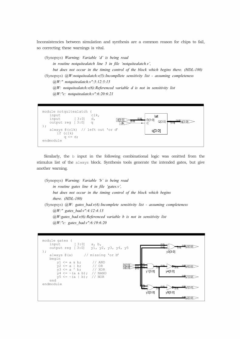
Inconsistencies between simulation and synthesis are a common reason for chips to fail, so correcting these warnings is vital.
(Synopsys) Warning: Variable ‘d’ is being read in routine notquitealatch line 5 in file ‘notquitealatch.v’, but does not occur in the timing control of the block which begins there. (HDL-180) (Synopsys) @W:notquitealatch.v(5):Incompllete sensitivity list - assuming completeness @W:" notquitealatch.v":5:12:5:15 @W: notquitealatch.v(6):Referenced variable d is not in sensitivity list @W:"c: notquitealatch.v":6:20:6:21
module notquitealatch ( input clk, input [3:0] d, output reg [3:0] q); always @(clk) // left out ‘or d’ if (clk) q <= d;endmodule
Similarly, the b input in the following combinational logic was omitted from the stimulus list of the always block. Synthesis tools generate the intended gates, but give another warning.
(Synopsys) Warning: Variable ‘b’ is being read in routine gates line 4 in file ‘gates.v’, but does not occur in the timing control of the block which begins there. (HDL-180) (Synopsys) @W: gates_bad.v(4):Incomplete sensitivity list - assuming completeness @W:" gates_bad.v":4:12:4:13 @W:gates_bad.v(6):Referenced variable b is not in sensitivity list @W:"c: gates_bad.v":6:19:6:20
module gates ( input [3:0] a, b, output reg [3:0] y1, y2, y3, y4, y5); always @(a) // missing ‘or b’ begin y1 <= a & b; // AND y2 <= a | b; // OR y3 <= a ̂ b; // XOR y4 <= ~(a & b); // NAND y5 <= ~(a | b); // NOR end endmodule
A.9.3 Missing begin/end Block
A.9.4 Undefined Outputs
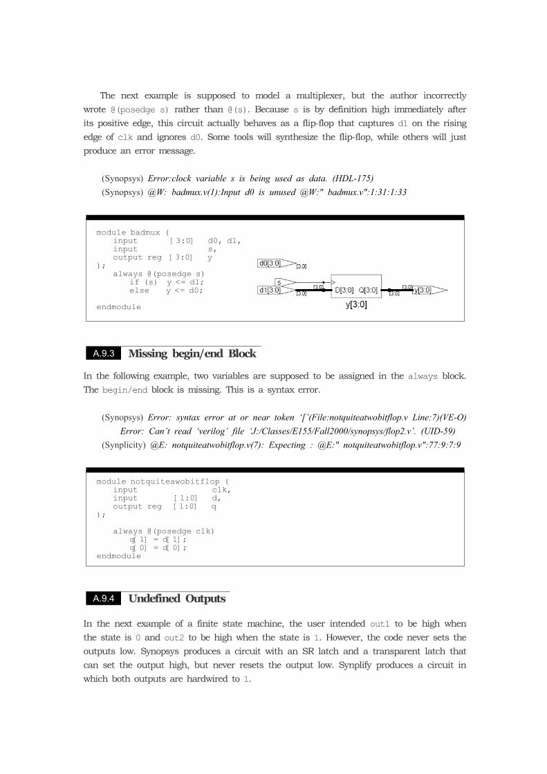
The next example is supposed to model a multiplexer, but the author incorrectly wrote @(posedge s) rather than @(s). Because s is by definition high immediately after its positive edge, this circuit actually behaves as a flip-flop that captures d1 on the rising edge of clk and ignores d0. Some tools will synthesize the flip-flop, while others will just produce an error message. (Synopsys) Error:clock variable s is being used as data. (HDL-175) (Synopsys) @W: badmux.v(1):Input d0 is unused @W:" badmux.v":1:31:1:33
module badmux ( input [3:0] d0, d1, input s, output reg [3:0] y); always @(posedge s) if (s) y <= d1; else y <= d0;
endmodule
In the following example, two variables are supposed to be assigned in the always block. The begin/end block is missing. This is a syntax error.
(Synopsys) Error: syntax error at or near token ‘[’(File:notquiteatwobitflop.v Line:7)(VE-O) Error: Can’t read ‘verilog’ file ‘J:/Classes/E155/Fall2000/synopsys/flop2.v’. (UID-59) (Synplicity) @E: notquiteatwobitflop.v(7): Expecting : @E:" notquiteatwobitflop.v":77:9:7:9
module notquiteawobitflop ( input clk, input [1:0] d, output reg [1:0] q);
always @(posedge clk) q[1] = d[1]; q[0] = d[0];endmodule
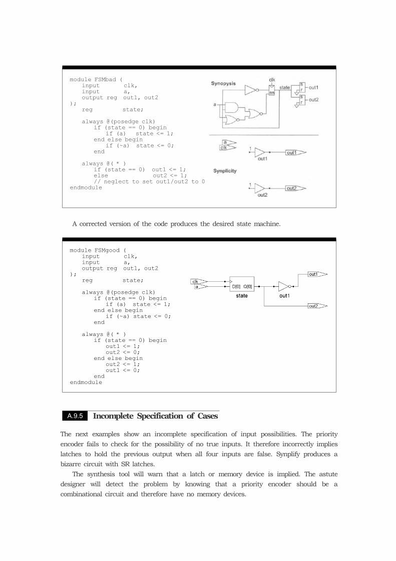
In the next example of a finite state machine, the user intended out1 to be high when the state is 0 and out2 to be high when the state is 1. However, the code never sets the outputs low. Synopsys produces a circuit with an SR latch and a transparent latch that can set the output high, but never resets the output low. Synplify produces a circuit in which both outputs are hardwired to 1.
A.9.5 Incomplete Specification of Cases
module FSMbad ( input clk, input a, output reg out1, out2); reg state;
always @(posedge clk) if (state == 0) begin if (a) state <= 1; end else begin if (~a) state <= 0; end
always @( * ) if (state == 0) out1 <= 1; else out2 <= 1; // neglect to set out1/out2 to 0endmodule
A corrected version of the code produces the desired state machine.
module FSMgood ( input clk, input a, output reg out1, out2); reg state;
always @(posedge clk) if (state == 0) begin if (a) state <= 1; end else begin if (~a) state <= 0; end
always @( * ) if (state == 0) begin out1 <= 1; out2 <= 0; end else begin out2 <= 1; out1 <= 0; endendmodule
The next examples show an incomplete specification of input possibilities. The priority encoder fails to check for the possibility of no true inputs. It therefore incorrectly implies latches to hold the previous output when all four inputs are false. Synplify produces a bizarre circuit with SR latches. The synthesis tool will warn that a latch or memory device is implied. The astute designer will detect the problem by knowing that a priority encoder should be a combinational circuit and therefore have no memory devices.
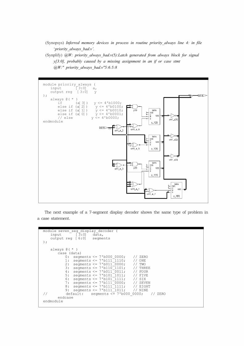
(Synopsys) Inferred memory devices in process in routine priority_always line 4: in file ‘priority_always_bad.v’. (Synplify) @W: priority_always_bad.v(5):Latch generated from always block for signal y[3:0], probably caused by a missing assignment in an if or case stmt @W:" priority_always_bad.v"5:6:5:8
module prioriry_always ( input [3:0] a, output reg [3:0] y); always @( * ) if (a[3]) y <= 4'b1000; else if (a[2]) y <= 4'b0100; else if (a[1]) y <= 4'b0010; else if (a[0]) y <= 4'b0001; // else y <= 4'b0000;endmodule
The next example of a 7-segment display decoder shows the same type of problem in a case statement.
module seven_seg_display_decoder ( input [3:0] data, output reg [6:0] segments);
always @( * ) case (data) 0: segments <= 7'b000_0000; // ZERO 1: segments <= 7'b111_1110; // ONE 2: segments <= 7'b011_0000; // TWO 3: segments <= 7'b110_1101; // THREE 4: segments <= 7'b011_0011; // FOUR 5: segments <= 7'b101_1011; // FIVE 6: segments <= 7'b101_1111; // SIX 7: segments <= 7'b111_0000; // SEVEN 8: segments <= 7'b111_1111; // EIGHT 9: segments <= 7'b111_1011; // NINE// default: segments <= 7'b000_0000; // ZERO endcase endmodule
A.9.6 Shorted Outputs
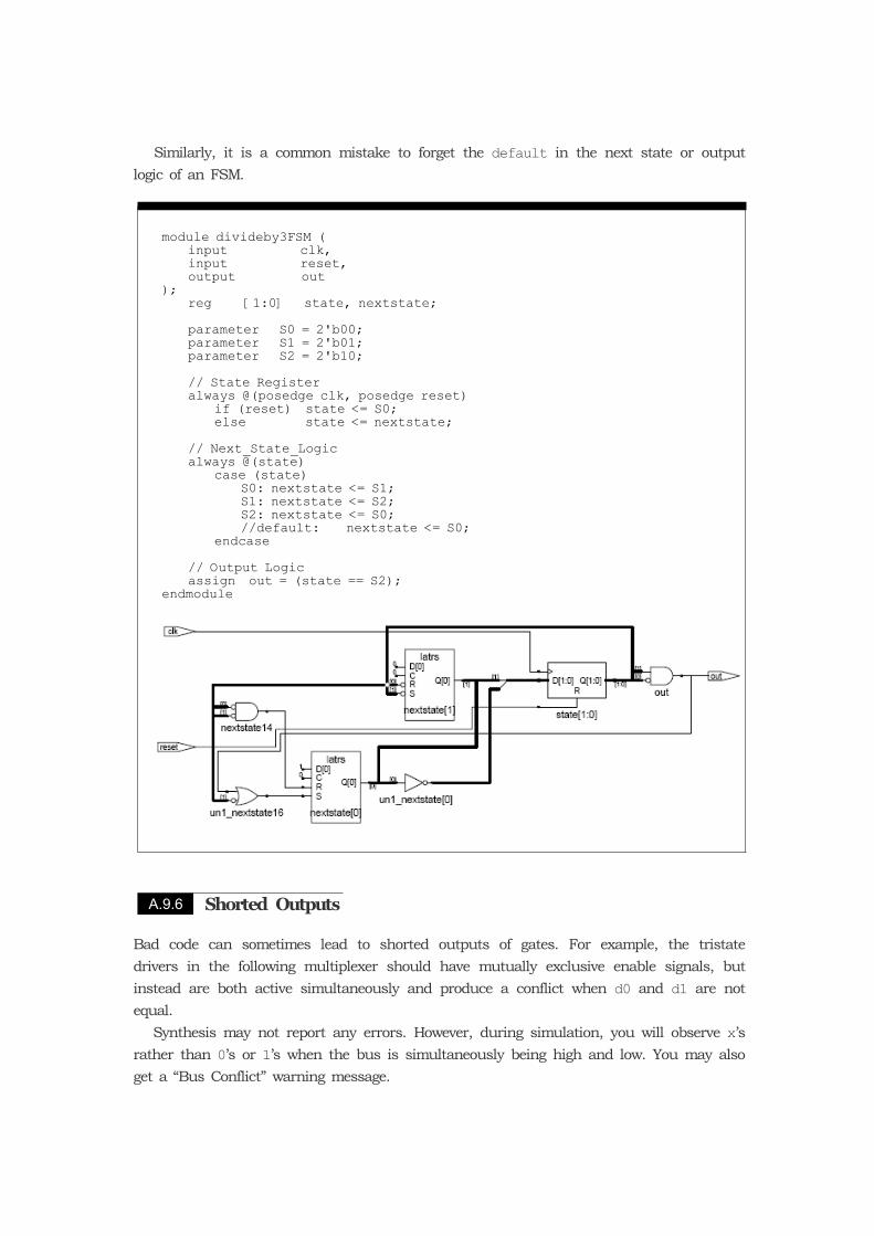
Similarly, it is a common mistake to forget the default in the next state or output logic of an FSM.
module divideby3FSM ( input clk, input reset, output out); reg [1:0] state, nextstate;
parameter S0 = 2'b00; parameter S1 = 2'b01; parameter S2 = 2'b10;
// State Register always @(posedge clk, posedge reset) if (reset) state <= S0; else state <= nextstate;
// Next_State_Logic always @(state) case (state) S0: nextstate <= S1; S1: nextstate <= S2; S2: nextstate <= S0; //default: nextstate <= S0; endcase
// Output Logic assign out = (state == S2);endmodule
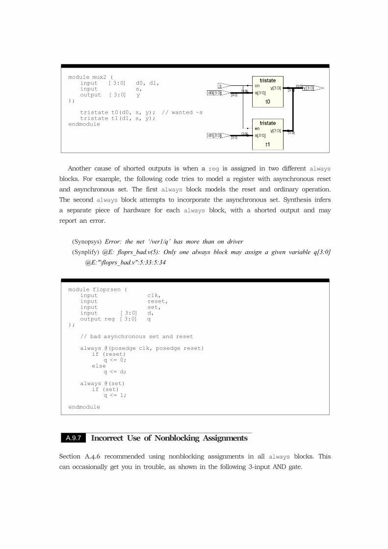
Bad code can sometimes lead to shorted outputs of gates. For example, the tristate drivers in the following multiplexer should have mutually exclusive enable signals, but instead are both active simultaneously and produce a conflict when d0 and d1 are not equal. Synthesis may not report any errors. However, during simulation, you will observe x’s rather than 0’s or 1’s when the bus is simultaneously being high and low. You may also get a “Bus Conflict” warning message.
A.9.7 Incorrect Use of Nonblocking Assignments
module mux2 ( input [3:0] d0, d1, input s, output [3:0] y);
tristate t0(d0, s, y); // wanted ~s tristate t1(d1, s, y);endmodule
Another cause of shorted outputs is when a reg is assigned in two different always blocks. For example, the following code tries to model a register with asynchronous reset and asynchronous set. The first always block models the reset and ordinary operation. The second always block attempts to incorporate the asynchronous set. Synthesis infers a separate piece of hardware for each always block, with a shorted output and may report an error.
(Synopsys) Error: the net ‘/ver1/q’ has more than on driver (Synplify) @E: floprs_bad.v(5): Only one always block may assign a given variable q[3:0] @E:"\floprs_bad.v":5:33:5:34
module floprsen ( input clk, input reset, input set, input [3:0] d, output reg [3:0] q);
// bad asynchronous set and reset
always @(posedge clk, posedge reset) if (reset) q <= 0; else q <= d; always @(set) if (set) q <= 1;
endmodule
Section A.4.6 recommended using nonblocking assignments in all always blocks. This can occasionally get you in trouble, as shown in the following 3-input AND gate.
A.10 Example: MIPS Processor
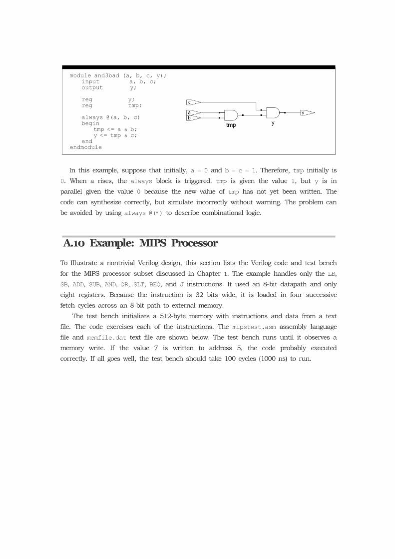
module and3bad (a, b, c, y); input a, b, c; output y;
reg y; reg tmp;
always @(a, b, c) begin tmp <= a & b; y <= tmp & c; end endmodule
In this example, suppose that initially, a = 0 and b = c = 1. Therefore, tmp initially is 0. When a rises, the always block is triggered. tmp is given the value 1, but y is in parallel given the value 0 because the new value of tmp has not yet been written. The code can synthesize correctly, but simulate incorrectly without warning. The problem can be avoided by using always @(*) to describe combinational logic.
To Illustrate a nontrivial Verilog design, this section lists the Verilog code and test bench for the MIPS processor subset discussed in Chapter 1. The example handles only the LB, SB, ADD, SUB, AND, OR, SLT, BEQ, and J instructions. It used an 8-bit datapath and only eight registers. Because the instruction is 32 bits wide, it is loaded in four successive fetch cycles across an 8-bit path to external memory. The test bench initializes a 512-byte memory with instructions and data from a text file. The code exercises each of the instructions. The mipstest.asm assembly language file and memfile.dat text file are shown below. The test bench runs until it observes a memory write. If the value 7 is written to address 5, the code probably executed correctly. If all goes well, the test bench should take 100 cycles (1000 ns) to run.