Embed Size (px)
Citation preview
Appendix ADelay Lines Realized with ElectronicLogic Circuits
This appendix discusses the realization of time-delay lines with unclocked logiccircuits, in particular with cascaded copier and inverter logic gates. In Sect. A.1,I discuss the method of implementing delay lines. In Sect. A.2, I use delay lines tomeasure the gate propagation time. In Sect. A.3, I discuss the difference betweencopier and inverter-based delay lines. In Sect. A.4, I measure the gate propagationdelay of XOR and multiplexer logic gates.1
A.1 Implementation of Delay Lines
Delay lines in electronic logic circuits can be implemented with various methods,such as by separating logic gates spatially as discussed in Sect. 3.3.2 or by discretizingtime and saving the Boolean state to memory [2]. Here, I implement delay lines byutilizing the propagation delay of logic gates.
The propagation time τLG of CMOS-based logic gates is caused by internalcapacitors that take a finite time to be charged and discharged before the outputsignal reaches the Boolean level [3].
I construct delay lines by cascading logic gates as shown inFig.A.1a. The resultingtime delay for a signal that travels through n cascaded logic gates is then
τn = nτLG, (A.1)
where τLG is the delay of a single logic gate including the delay of interconnectbetween two logic gates.
The logic gates are configured to use a single input and single output, so that theycan implement either the Boolean identity or inversion operation, corresponding to acopier or inverter gate. For most implementations of delay lines, I use inverter-baseddelay lines, which have the advantage of averaging the asymmetry in rise and fall
1 The method of constructing delay lines is published in Ref. [1].
© Springer International Publishing Switzerland 2015D.P. Rosin, Dynamics of Complex Autonomous Boolean Networks,Springer Theses, DOI 10.1007/978-3-319-13578-6
173

174 Appendix A: Delay Lines Realized with Electronic Logic Circuits
times as discussed in Sect. A.3. However, this makes it necessary that n is an evennumber to build non-inverting delay lines, which doubles the increments of adjustingtime delays. On the other hand, copier-based delay lines are useful when rectificationdue to differences in rise and fall times are wanted.
Thehardware description for an inverter-baseddelay line canbe found inSect. B.1.
A.2 Measurement of the Gate Propagation Delay
In this section, I show the linear relation in Eq. (A.1) and obtain the constant τLGand the heterogeneity in τLG. For this, I measure the time delay τn resulting from adelay line of n cascaded inverter gates for different n.
Figure A.1b shows the related setup that includes the delay line and an XOR logicgate. A voltage signal Vin is sent into the delay line, where Vin describes a singleBoolean transition. The output of the delay line is then given by Vτ (t) = Vin(t − τn)
as a delayed version of the input voltage; hence, the two voltages differ in Booleanstates for a time period given by the delay τn . I measure this difference of Booleanstates with an XOR logic gate, which outputs a high Boolean voltage (VXOR = VH )when the two input voltages differ [see its look-up table in Fig. 2.2a]. The resultingoutput voltage VXOR of the XOR gate is a pulse with a width corresponding to thelength of the delay line, which I measure with an external oscilloscope.
0 20 40 60 80 100n
0
10
20
30
(ns)
(b)
(c)
VH
VLt
VinVH
VLt
VXOR
(a)...=
Vin Vout
XORVin
VXOR
VoutVin
Fig. A.1 a Construction of a delay line with cascaded inverter gates. b Circuit to measure the timedelay. cMeasurement results of the time delay as a function of n (dots) and fit according to Eq. (A.1)(line)

Appendix A: Delay Lines Realized with Electronic Logic Circuits 175
I measure the full width at half maximum (FWHM) of the resulting pulse inVXOR for different n. The generated data, shown in Fig. A.1c, describes the linearrelationship of Eq. (A.1) with the best fit value τLG = 0.28 ± 0.01 ns and an errorestimate obtained from the goodness of the fit.
The propagation delay can also be obtained by constructing a ring oscillator andmeasuring the resulting frequency, as described in Sect. 6.2.5.1.
A.3 Difference Between Copier- and Inverter-Based DelayLines
To understand the difference between copier and inverter-based delay lines, I senda periodic signal into copier and inverter logic gates and measure the duty cycle ofinput and output. The duty cycle of a Boolean signal is defined as
D = TH
T, (A.2)
where the signal spends a time TH and TL in the Boolean high and low state, respec-tively, and hence the period is T = TH + TL .
After the signal propagates through a logic gate, the time spent in the high andlow Boolean voltage can change (TH = TH + r , TL = TL − r ) due to a differencein rise and fall time of r , which I call pulse lengthening, leading to an altered dutycycle of
D = TH + r
T. (A.3)
I find that a single logic gate leads to pulse lengthening of r = 24 ps for copierlogic gates. Figure A.2 shows the output waveform of copier-based delay lines ofdifferent length n with a periodic input signal. The pulse lengthening effect increaseswith n, resulting in a duty cycle of
D = TH + nr
T. (A.4)
When the signal propagates through long enough copier-based delay lines, pulsesgrow so much that the duty cycle becomes D = 1, pulses merge, and the oscillationsare pruned. Then, the output stays constantly in the Boolean high state even thoughthe input is oscillatory as shown in Fig. A.2d. I utilize this effect in Chap. 6 as alow-pass filter in phase-locked loops.
For cascaded inverter logic gates, on the other hand, the pulse lengthening cancelsout in every pair of two inverter logic gates. Therefore, chains of inverter gates displaya much smaller change in pulse width that I measure to be only r = ±1.4 ps per pairof inverter logic gates (depending on the specific realization), which is more than two

176 Appendix A: Delay Lines Realized with Electronic Logic Circuits
0.00.51.01.5
V (
V)
0.00.51.01.5
V (
V)
0.00.51.01.5
V (
V)
0 100 200 300 400 500
0.00.51.01.5
V (
V)
(a)
(b)
(c)
(d)
t (ns)
Fig. A.2 Pulse lengthening for an input signal of frequency 9MHz and duty cycle 96.4%. Theinput signal shown in (a) propagates through 50, 100, and 150 copier gates, leading to output signalsshown in (b), (c) and (d), respectively
orders of magnitude decreased and more than one order of magnitude smaller than incascaded copiers. This value of r results from heterogeneity in the pulse lengthening.
A.4 Delay of Different Logic Gates
The propagation delay of inverter gates is measured in Sect. A.2 by comparing aBoolean transition and its delayed version with an XOR gate. The delay can also bemeasured by constructing ring oscillators as described in Sect. 6.2.5.1 andmeasuringthe frequency. With this second method, I measure the propagation delay of differentlogic gates used in this thesis as shown in Table A.1.
Buffer and inverter gates with an in-degree of one have the shortest gate prop-agation delay. For gates with higher in-degree, the propagation delay increases,which is because of longer paths in the look-up table block for larger in-degrees(see Sect. 3.2.1). Note that the measurement in Sect. A.2 leads to a propagationdelay of inverter logic gates of τLG = 0.28 ± 0.01 ns, which is 7% higher than themeasurement with ring oscillators. This difference is mainly due to the number oflogic gates used to construct delay lines. In this section, the delay lines are constructedwith 16 logic gates, fitting into a single logic-array block (LAB), hence excludingthe delay of wire connections between LABs. On the other hand, the measurementin Sect. A.2 included 100 logic gates to average heterogeneity (see also Sect. 3.2.1).
Appendix A: Delay Lines Realized with Electronic Logic Circuits 177
Table A.1 Measurements of the period generated by a ring oscillator that includes a ring of 15logic gates of the type named in the left column and either one inverter gate or one buffer gate togenerate inverted delayed feedback. The right column shows the derived gate propagation delay.The open inputs are connected to switches on the FPGA development board
Type T (ns) τ (ns)
Inverter 8.31 0.26 ± 0.01
Buffer 8.39 0.26 ± 0.01
2-input OR 11.28 0.36 ± 0.02
3-input XNOR 12.58 0.38 ± 0.02
3-input MUX 12.08 0.38 ± 0.02

Appendix BHardware Descriptions and NumericalAlgorithms
This appendix shows the hardware description of the autonomous logic circuits inthis thesis using the hardware description language Verilog. It also discusses thenumerical algorithm for numerical simulations.
The hardware description can be used to implement the circuit on various FPGAs,but it was tested specifically on the Altera Cyclone IV FPGA with model numberEP4CE115F29C7N. For an explanation of the syntax of Verilog, see Sect. 3.3.1 andRef. [4].
B.1 Inverter-Based Delay Lines
The following hardware description realizes an inverter-based delay line used inmostof the following hardware designs.
1 module my_delay_line(s_in , s_out ) ;2 parameter n=20;3 genvar i ;4 input s_in ;5 output s_out ;6 wire [n−1:0] delay /∗ synthesis keep ∗/ ;7 assign delay[0] = ~s_in ;8 assign s_out = delay[n−1];9 generate10 for ( i=0; i < n−1; i=i+1)11 begin : generate_delay12 assign delay [ i+1] = ~delay [ i ] ;13 end14 endgenerate15 endmodule
© Springer International Publishing Switzerland 2015D.P. Rosin, Dynamics of Complex Autonomous Boolean Networks,Springer Theses, DOI 10.1007/978-3-319-13578-6
179

180 Appendix B: Hardware Descriptions and Numerical Algorithms
This module, called “my_delay_line,” implements a delay line of invertergates as discussed in Sect. A.1. The hardware module has an input wire “s_in” andoutput wire “s_out,” where the input signal is sent into the chain of “n” invertergates and the output is the resulting signal after the last inverter gate. The parameter“n” can be defined when this hardware module is initiated. The inverter logic gatesare generated with the “assign” statement within a “generate” “for” loop. Forfurther information see Sect. 3.3.1.
B.2 Delayed-Feedback XNOR Oscillator
The following hardware description realizes the delayed-feedback XNOR oscillatoras introduced in Sect. 4.3. It implements the delay line module defined above.
1 module main(out ) ;2 output out ;3 wire [3:0] net /∗synthesis keep∗/ ;4 assign net[0] = ~(net[1] ^ net[2] ^ net [3]);5 my_delay_line #(10) delay1(net [0] , net [1]);6 my_delay_line #(6) delay2(net [0] , net [2]);7 my_delay_line #(12) delay3(net [0] , net [3]);8 assign out = net [0];9 endmodule
Here, the instantiations of “my_delay_line” are called “delay1,” “delay2,”and “delay3,” so that they can be referred in other design tools. The delay lines areinstantiated with the parameter “n” using the notation of “#(10)” to set the numberof inverter gates included in the delay lines. I include an XNOR gate that is definedwith an inversion “˜” and XOR “ˆ” operator and has the three inputs “net[1],”“net[2],” “net[3]” and the output “net[0].” The output of the XNOR logicgate “net[0]” is input to the three delay lines that feed back to the inputs of thelogic gate. The output port of the FPGA, called “out,” is connected to the output ofthe XNOR logic gate “net[0].”
B.3 Random Number Generator
In this section, I discuss thehardwaredescriptions used for randomnumber generationin Chap. 5.

Appendix B: Hardware Descriptions and Numerical Algorithms 181
B.3.1 XOR Ring Oscillator
The following is the hardware description for the hybrid Boolean network used forrandom number generation in Sect. 5.3.
1 module rng(CLOCK_100, word_out) ;2 parameter N=16;3 input CLOCK_100;4 output reg word_out;5 wire [N:0] net /∗synthesis keep∗/ ;6 reg [3:0] tr ig ;7 genvar i ;89 /∗autonomous Boolean nodes∗/10 assign net[0] = ~(net [N−1] ^ net[0]^ net [1]);11 assign net [N−1] = (net [N−2] ^ net [N−1] ^ net [0]);12 generate13 for ( i=1; i < N−1; i=i+1)14 begin : generate_ring15 assign net [ i ] = (net [ i−1] ^ net [ i ] ^ net [ i +1]);16 end17 endgenerate1819 /∗synchronous Boolean node∗/20 always @ (negedge CLOCK_100)21 begin22 tr ig [0] = net [0];23 tr ig [1] = net [4];24 tr ig [2] = net [8];25 tr ig [3] = net [12];26 end27 always @ (posedge CLOCK_100)28 begin29 word_out = tr ig [0] ^ tr ig [1] ^ tr ig [2] ^ tr ig [3];30 end3132 endmodule
It has a 1-bit input for the clock and a 1-bit output for the synchronous randombit. The parameter N gives the number of autonomous nodes and is set to N = 16,so that the synchronous node gets input from every fourth autonomous node in thenetwork.
Lines 9–17 implement the autonomous Boolean nodes with the XNOR gate inline 10 and the last XOR gate in line 11. The autonomous nodes have outputs givenby an vector of N wires “net.” Lines 12–17 implement the remaining N − 2 XOR

182 Appendix B: Hardware Descriptions and Numerical Algorithms
gates using a “for” loop. The XOR gates have have inputs from the left and rightneighbor and from itself.
The synchronous node has an output register “word_out” and an input register“trig.” These are implemented using flip-flops with “always@” statements withthe wire “clock_100” connected to the clock port. Flip-flops are implementedbefore and after the synchronous node. The clock can have any frequency, wherefrequencies that are too high lead to inferior random numbers and clcok frequenciesthat are too low do not exploit the achievable speed as discussed in Sect. 5.3. Theused hardware board, the Terasic DE2-115, supplies a 50MHz clock that can be usedto generate clock signals of different frequencies using a phase-locked loop using aso-called mega-function.
B.3.2 Transfer of Random Numbers to a computer
The hybrid Boolean network from the previous section generates a binary stream ofrandom numbers. These are transferred to a computer using another FPGA board, asshown in Fig. B.1. The hybrid Boolean network has one input, the 100MHz clock,and one output, the random number bit stream, which are connected to the SMAinput and output connectors on the FPGA board. Another FPGA board generates theclock and receives the random numbers.
This board saves 1Mbit of data (coming from the other board) into SRAM, thensending this data via TCP/IP protocol to a computer. This is repeated 1,000 times toachieve a file size of 1Gbit. The trasfer protocol requires a processor structure onthe FPGA, which is achieved using the NIOS II softcore processor. The processoris programmed to be the socket server and a desktop computer is programmed to bethe client. The C-code used for both server and client can be found in Ref. [5].
B.3.3 XOR Ring Networks in Parallel
For implementing random number generators in parallel, the hardware descriptionin Sect. B.3.1 called “rng” is instantiated 128 times as follows.
1 module rng_parallel (clk , rng_out ) ;2 parameter n_rng=128;3 input CLOCK_100;4 output [127:0] rng_out ;5 genvar i ;6 generate7 for ( i=0; i < n_rng−1; i=i+1)8 begin : generate_multiple_rngs9 rng inst (CLOCK_100, rng_out[ i ] ) ;10 end11 endgenerate12 endmodule
Appendix B: Hardware Descriptions and Numerical Algorithms 183
A
B
C
D 4 4 1flip-flop
XOR
ABCD
Ethernet connection to computer
NIOS II Softcoreprocessor,implementingTCP/IP socket server
hybrid Boolean network, generating random numbers
100 MHzclock
100 MHzclock
0011010data
SRAM
FPGA
FPGA
Fig. B.1 Schematic of the transfer of random numbers to the computer. Two FPGA boards areconnected via general purpose input outputs (GPIO) to send random numbers from one board to theother at 100Mbit/s. The receiving board implements a NIOS II softcore processor for the transfer ofrandom numbers via TCP/IP protocol to a computer. The left board implements the hybrid Booleannetwork shown with a graphic similar to Fig. 5.3a
A “for” loop implements 128 random number generators.For the transfer of random numbers, the data is first saved to on-chip memory
with word sizes of 128 bits at 100MHz, which is a FIFO (first in, first out) buffer.Then, the memory is read at a lower rate of 100Mbit/s to another board as describedin Sect. B.3.2 (see also Fig. 5.11).
B.4 Modified Ring Oscillators
The hardware description for a modified ring oscillators is as follows, with a logiccircuit shown in Fig. 5.7 and discussed in Sect. 6.3.
1 module mod_ring_osc( in , out ) ;2 parameter n=20;3 input in ;4 output out ;
184 Appendix B: Hardware Descriptions and Numerical Algorithms
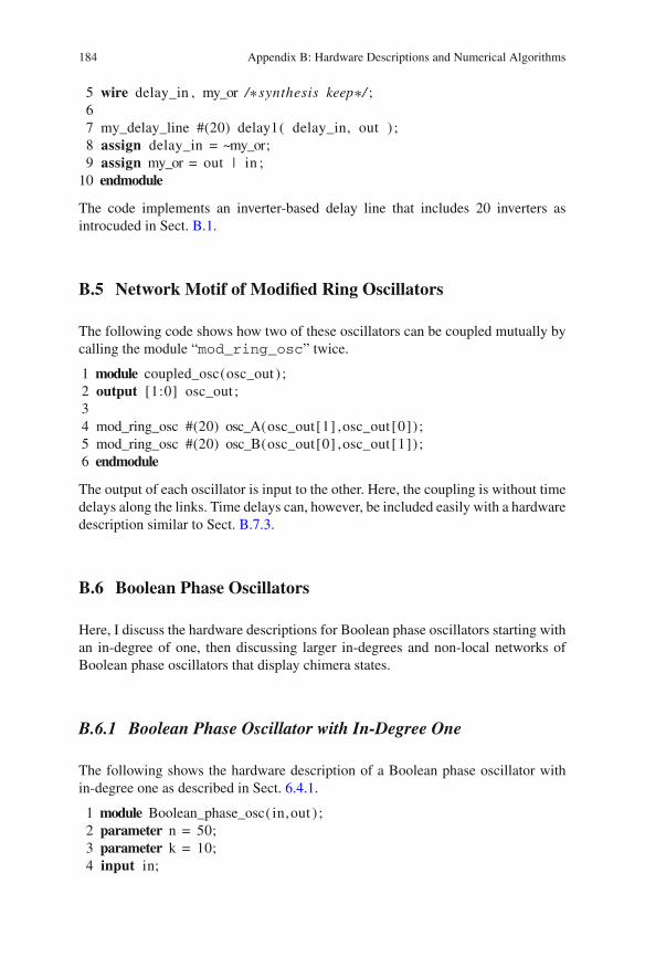
5 wire delay_in , my_or /∗synthesis keep∗/ ;67 my_delay_line #(20) delay1( delay_in, out ) ;8 assign delay_in = ~my_or;9 assign my_or = out | in ;10 endmodule
The code implements an inverter-based delay line that includes 20 inverters asintrocuded in Sect. B.1.
B.5 Network Motif of Modified Ring Oscillators
The following code shows how two of these oscillators can be coupled mutually bycalling the module “mod_ring_osc” twice.
1 module coupled_osc(osc_out ) ;2 output [1:0] osc_out ;34 mod_ring_osc #(20) osc_A(osc_out[1] ,osc_out [0]);5 mod_ring_osc #(20) osc_B(osc_out[0] ,osc_out [1]);6 endmodule
The output of each oscillator is input to the other. Here, the coupling is without timedelays along the links. Time delays can, however, be included easily with a hardwaredescription similar to Sect. B.7.3.
B.6 Boolean Phase Oscillators
Here, I discuss the hardware descriptions for Boolean phase oscillators starting withan in-degree of one, then discussing larger in-degrees and non-local networks ofBoolean phase oscillators that display chimera states.
B.6.1 Boolean Phase Oscillator with In-Degree One
The following shows the hardware description of a Boolean phase oscillator within-degree one as described in Sect. 6.4.1.
1 module Boolean_phase_osc( in,out ) ;2 parameter n = 50;3 parameter k = 10;4 input in;

Appendix B: Hardware Descriptions and Numerical Algorithms 185
5 output out;67 wire [n:0] osc /∗synthesis keep∗/ ;8 wire mux_out, xor_sig /∗synthesis keep∗/ ;910 assign out = mux_out;11 assign osc[0] = ~mux_out;12 assign xor_sig = out ^ in;13 assign mux_out = xor_sig ? osc[n−k] : osc[n] ;1415 genvar i;16 generate17 for( i=0;i<n; i=i+1)18 begin : building_delay19 assign osc[ i+1] = osc[ i ] ;20 end21 endgenerate22 endmodule
Here, the two parameters “n” and “k” determine the natural frequency and the cou-pling strength as described in Sect. 6.4.1 and can be adjusted to change the oscillator’sproperties. The code implements one inverter gate (line 11), a multiplexer (line 13),an XOR gate (line 12), and 50 buffer gates for the delay (line 15–20), leading to 53logic gates in total. The multiplexer chooses between the output of the buffer-baseddelay line “osc[n-k]” and “osc[n],” leading to a delay difference correspondingto “k” buffer gates.
Boolean phase oscillators can be coupled unidirectionally as follows
1 module unidir_coupling(driver,osc ) ;2 input driver ;3 output osc ;45 Boolean_phase_osc #(.n(50) ,.k(10)) osc_A(driver , osc ) ;6 endmodule
Here, the Boolean signal “driver” is input to the Boolean phase oscillator with out-put “osc.” The notation “#(.n(50),.k(10))” redefines the parameters withinthemodule. By scanning a range of frequencies of “driver” and comparing the out-put frequency of “osc,” a devil’s staircase can be recorded as discussed in Sect. 6.4.2.
Boolean phase oscillators can be coupled bidirectionally as follows
1 module bidir_coupling(osc ) ;2 output [1:0] osc ;34 Boolean_phase_osc #(.n(50) ,.k(10)) osc_A(osc[1] ,osc[0]);5 Boolean_phase_osc #(.n(50) ,.k(10)) osc_B(osc[0] ,osc[1]);6 endmodule

186 Appendix B: Hardware Descriptions and Numerical Algorithms
By changing the parameters n and k in the two oscillators, the bidirectional cou-pling plane in Sect. 6.4.4 can be measured. The measurment in that section, however,was automized with labview by implementing several oscillator combinations on theFPGA and selecting and measuring them without changing the hardware implemen-tation on the FPGA.
B.6.2 Boolean Phase Oscillator with Large In-Degree
The following hardware description results in a Boolean phase oscillator with anin-degree of 60 as discussed in Chap. 7.
1 module bpo_node(node_out , c_signal, c_disable ) ;2 parameter n_delay=30, k=1;3 genvar i ;4 input [59:0] c_signal /∗synthesis keep∗/ ;5 output node_out;6 input [59:0] c_disable ;7 wire [n_delay−1:0] main_delay /∗synthesis keep∗/ ;8 wire [59:0] mux_out /∗synthesis keep∗/ ;9 wire [59:0] k_delay0 /∗synthesis keep∗/ ;10 wire [59:0] k_delay1 /∗synthesis keep∗/ ;11 . . .12 wire [59:0] k_delay59 /∗synthesis keep∗/ ;1314 assign node_out = mux_out[0];1516 / / define multiplexer17 assign mux_out[0] = c_disable[0] ? k_delay0[k−1] :18 (c_signal[0] ? mux_out[1] : k_delay0[k−1]);19 assign mux_out[1] = c_disable[1] ? k_delay1[k−1] :20 (c_signal[1] ? mux_out[2] : k_delay1[k−1]);21 . . .22 assign mux_out[59] = c_disable[59] ? k_delay59[k−1] :23 (c_signal[59] ? main_delay[n_delay−1] :24 k_delay59[k−1]);2526 / / define main main_delay27 assign main_delay[0] = ~mux_out[0];28 generate29 for( i=0; i<n_delay−1; i=i+1)30 begin : build_main_delay31 assign main_delay[ i+1] = main_delay[ i ] ;32 end

Appendix B: Hardware Descriptions and Numerical Algorithms 187
33 endgenerate3435 / / define k−coupling delays36 assign k_delay0[0] = mux_out[1];37 generate38 for( i=0; i<k−1; i=i+1)39 begin : build_k_delay040 assign k_delay0[ i+1] = k_delay0[ i ] ;41 end42 endgenerate4344 assign k_delay1[0] = mux_out[2];45 generate46 for( i=0; i<k−1; i=i+1)47 begin : build_k_delay148 assign k_delay1[ i+1] = k_delay1[ i ] ;49 end50 endgenerate5152 . . .5354 assign k_delay59[0] = main_delay[n_delay−1];55 generate56 for( i=0; i<k−1; i=i+1)57 begin : build_k_delay5958 assign k_delay59[ i+1] = k_delay59[ i ] ;59 end60 endgenerate61 endmodule
The Verilog code for the Boolean phase oscillator with an in-degree of 60 has threeconnections “node_out,” “c_signal,” and “c_disable.” “node_out” is anoutput wire with the dynamics of the oscillator. “c_signal” and “c_disable”are vectors of 60 input wires, corresponding to the in-degree of the oscillator.“c_signal” includes the state of the phase comparisons to adjust the delay line and“c_disable” includes signals to disable the input connections used to uncoupleoscillators. For example, all wires “c_disable” can be set to the Boolean highstate to measure the natural frequency of the oscillator.
The circuit diagram with indicated wire names is shown in Fig. B.2. The figureshows that the “c_disable” wires are input to the multiplexers together with thecoupling signals “c_signal.”When one “c_disable”wire is chosen at Boolean“1,” the longer time delay line of that multiplexer is selected independently of thecorresponding “c_signal.” On the other hand, when it is “0,” the multiplexer canswitch depending on the corresponding “c_signal.” ABoolean “1” “c_signal”signal selects the output of the previous multiplexer or the output of the fixed delay
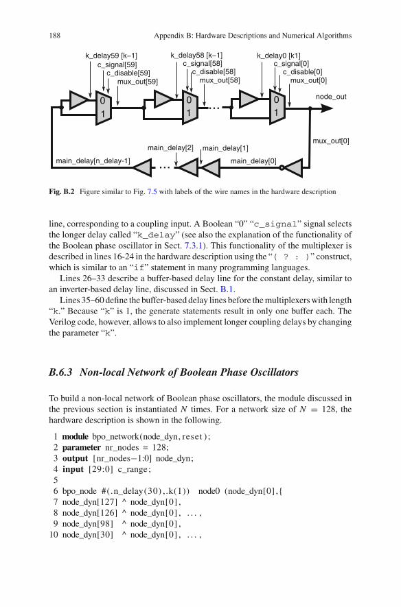
188 Appendix B: Hardware Descriptions and Numerical Algorithms
...11
01
0
...
mux_out[0]
node_out
c_disable[0]c_signal[0]
mux_out[58]c_disable[58]
c_signal[58]
mux_out[59]c_disable[59]
c_signal[59]
main_delay[0]
mux_out[0]main_delay[1]main_delay[2]
main_delay[n_delay-1]
k_delay59 [k−1] k_delay58 [k−1] k_delay0 [k1]
0
Fig. B.2 Figure similar to Fig. 7.5 with labels of the wire names in the hardware description
line, corresponding to a coupling input. A Boolean “0” “c_signal” signal selectsthe longer delay called “k_delay” (see also the explanation of the functionality ofthe Boolean phase oscillator in Sect. 7.3.1). This functionality of the multiplexer isdescribed in lines 16-24 in the hardware description using the “( ? : )” construct,which is similar to an “if” statement in many programming languages.
Lines 26–33 describe a buffer-based delay line for the constant delay, similar toan inverter-based delay line, discussed in Sect. B.1.
Lines 35–60define the buffer-based delay lines before themultiplexerswith length“k.” Because “k” is 1, the generate statements result in only one buffer each. TheVerilog code, however, allows to also implement longer coupling delays by changingthe parameter “k”.
B.6.3 Non-local Network of Boolean Phase Oscillators
To build a non-local network of Boolean phase oscillators, the module discussed inthe previous section is instantiated N times. For a network size of N = 128, thehardware description is shown in the following.
1 module bpo_network(node_dyn, reset ) ;2 parameter nr_nodes = 128;3 output [nr_nodes−1:0] node_dyn;4 input [29:0] c_range ;56 bpo_node #(.n_delay(30) ,.k(1)) node0 (node_dyn[0] ,{7 node_dyn[127] ^ node_dyn[0] ,8 node_dyn[126] ^ node_dyn[0] , . . . ,9 node_dyn[98] ^ node_dyn[0] ,10 node_dyn[30] ^ node_dyn[0] , . . . ,
Appendix B: Hardware Descriptions and Numerical Algorithms 189
11 node_dyn[1] ^ node_dyn[0]} ,12 {c_range[0] , . . . , c_range[29] , c_range[29] ,13 c_range[28] , . . . , c_range[0]});1415 bpo_node #(.n_delay(30) ,.k(1)) node1 (node_dyn[1] ,{16 node_dyn[127] ^ node_dyn[1] ,17 node_dyn[126] ^ node_dyn[1] , . . . ,18 node_dyn[99] ^ node_dyn[1] ,19 node_dyn[31] ^ node_dyn[1] , . . . ,20 node_dyn[0] ^ node_dyn[1]} ,21 {c_range[1] , . . . , c_range[29] , c_range[29] , . . . ,22 c_range[1] , c_range[0] , c_range[0]});2324 . . .2526 bpo_node #(.n_delay(30) ,.k(1)) node127 (node_dyn[127],27 {node_dyn[126] ^ node_dyn[127], . . . ,28 node_dyn[97] ^ node_dyn[127],29 node_dyn[29] ^ node_dyn[127], . . . ,30 node_dyn[0] ^ node_dyn[127]},31 {c_range[0] , . . . , c_range[29] , c_range[29] , . . . ,32 c_range[0]});33 endmodule
Here, the module has an output vector of 128 wires that are connected tothe Boolean dynamical variables of the nodes and an input vector of 30 wires“c_range” to adjust the coupling range (see also Sect. 7.2.2.1).
The 128 nodes are instantiated with the coupling strength “k= 1” and constantdelay “n_delay= 30”. The latter parameter can be adjusted in the network so thatfrequency heterogeneity is reduced.
For the first Boolean phase oscillator in lines 6–13, the output wire is connectedto “node_dyn[0].” The 60 node input wires are connected to an XOR phasedetector given by “node_dyn[127] ˆ node_dyn[0],” where the first numberdenotes the number of the oscillator that the signal is compared with. These XORoperations are sorted by node numbers such that the operation with the highest nodenumber comes first. The signals “c_range” that disable input couplings are assem-bled such that the coupling range is set by the number of 1 bits in “c_range”filled up from the first bit. For example, a coupling radius of R = 1 is achievedwith “c_range[0]=1” and “c_range[i“]=0” for i > 0, where only the cou-pling inputs with “node_dyn[127]” and “node_dyn[1]” are activated (for“node_dyn[0]”).
This code is repeated for all 128 oscillators as shown in lines 15–31.The oscillators are assembled on the chip using the chip planner as discussed in
Fig. 7.6.
190 Appendix B: Hardware Descriptions and Numerical Algorithms
For the readout of the network dynamics “node_dyn,” the wire states are savedto on-chip memory and then sent to a computer via a RS-232 connection.
B.7 Boolean Neurons
In this section, I discuss the hardware description of Boolean neurons, of a networkmotif of Boolean neurons, and of an interconnected ring network of Boolean neurons.
B.7.1 Pulse Generator
The Boolean neurons, as described in Sect. 8.3.1, are based on pulse generators. Thehardware description of such a device is shown in the following.
1 module pulse_generator ( sig_in,pulse_out ) ;2 parameter n_delay = 5;3 input sig_in ;4 output pulse_out ;5 reg state , state_inverse ;6 wire delayed_state ;78 always @(posedge sig_in )9 state <= ~state ;1011 my_delay_line #(n_delay) inst0 ( state ,delayed_state ) ;12 assign pulse_out = state ^ delayed_state ;13 endmodule
Here, the “always” construct implements aflip-flop,where the register “state”changes its Boolean value when the input signal “sig_in” has a positive edge.The module “my_delay_line” instantiates a delay line of “n_delay” invertergates, as introduced in Sect. B.1. The result is the circuit shown in Fig. 8.7a with“n_delay” inverter gates.
B.7.2 Boolean Neuron
Using two pulse generators, a Boolean neuron can be implementedwith the followinghardware description.

Appendix B: Hardware Descriptions and Numerical Algorithms 191
1 module Boolean_neuron( in , out ) ;2 parameter n_ref = 10;3 parameter n_pulse = 2;4 input in ;5 output out ;6 wire and_out , refr ;78 assign and_out = ~refr & in ;9 pulse_generator #(n_pulse) unit0 (and_out , out ) ;10 pulse_generator #(n_ref) unit1 (and_out , refr ) ;11 endmodule
TheBoolean neuron has an input and output wire and can be configuredwith para-meters “n_ref” and “n_pulse.” It implements the neuron according to Fig. 8.7bwith an NAND gate (inversion of AND) in line 8.
B.7.3 Network Motif of Two Bidirectionally-Coupled BooleanNeurons
The following shows the hardware description of the bidirectional coupling topologyin Sect. 8.4.2 according to the circuit diagram in Fig. 8.10b.
1 module bidir_coupling(exc_out , reset ) ;2 output [1:0] exc_out ;3 input reset ;4 wire [1:0] exc_in , couplingK, couplingC;56 / / nodes7 assign exc_in[0] = ( init ialpulse | couplingC[1] |8 couplingK[0]) & ~reset ;9 Boolean_neuron #(10,4) node0(exc_in[0] , exc_out [0]);10 assign exc_in[1] = ( couplingC[0] |11 couplingK[1]) & ~reset ;12 Boolean_neuron #(10,4) node1(exc_in[1] , exc_out [1]);1314 / / links15 my_delay_line #(40) C0(exc_out[0] ,couplingC[0]);16 my_delay_line #(40) K0(exc_out[0] ,couplingK[0]);17 my_delay_line #(40) C1(exc_out[1]couplingC[1]);18 my_delay_line #(40) K1(exc_out[1] ,couplingK[1]);19 endmodule
This hardwaremodule has an output vector of twowires “exc_out” and an inputwire “reset,” where the first provides the dynamics of the twoBoolean neurons and
192 Appendix B: Hardware Descriptions and Numerical Algorithms
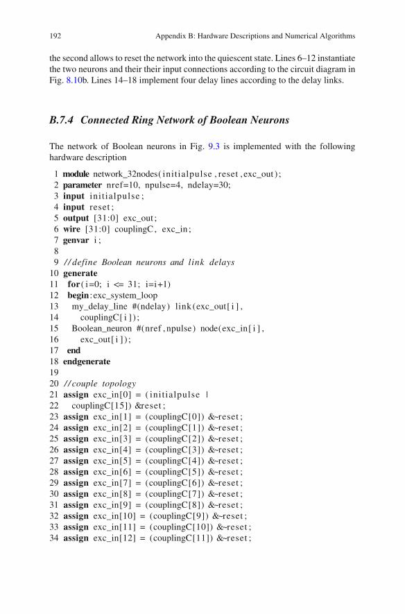
the second allows to reset the network into the quiescent state. Lines 6–12 instantiatethe two neurons and their their input connections according to the circuit diagram inFig. 8.10b. Lines 14–18 implement four delay lines according to the delay links.
B.7.4 Connected Ring Network of Boolean Neurons
The network of Boolean neurons in Fig. 9.3 is implemented with the followinghardware description
1 module network_32nodes( initialpulse , reset , exc_out ) ;2 parameter nref=10, npulse=4, ndelay=30;3 input init ialpulse ;4 input reset ;5 output [31:0] exc_out ;6 wire [31:0] couplingC, exc_in ;7 genvar i ;89 / / define Boolean neurons and link delays10 generate11 for( i=0; i <= 31; i=i+1)12 begin :exc_system_loop13 my_delay_line #(ndelay) link (exc_out[ i ] ,14 couplingC[ i ] ) ;15 Boolean_neuron #(nref , npulse) node(exc_in[ i ] ,16 exc_out[ i ] ) ;17 end18 endgenerate1920 / / couple topology21 assign exc_in[0] = ( init ialpulse |22 couplingC[15]) &reset ;23 assign exc_in[1] = (couplingC[0]) &~reset ;24 assign exc_in[2] = (couplingC[1]) &~reset ;25 assign exc_in[3] = (couplingC[2]) &~reset ;26 assign exc_in[4] = (couplingC[3]) &~reset ;27 assign exc_in[5] = (couplingC[4]) &~reset ;28 assign exc_in[6] = (couplingC[5]) &~reset ;29 assign exc_in[7] = (couplingC[6]) &~reset ;30 assign exc_in[8] = (couplingC[7]) &~reset ;31 assign exc_in[9] = (couplingC[8]) &~reset ;32 assign exc_in[10] = (couplingC[9]) &~reset ;33 assign exc_in[11] = (couplingC[10]) &~reset ;34 assign exc_in[12] = (couplingC[11]) &~reset ;

Appendix B: Hardware Descriptions and Numerical Algorithms 193
35 assign exc_in[13] = (couplingC[12]) &~reset ;36 assign exc_in[14] = (couplingC[21] |37 couplingC[13]) &~reset ;38 assign exc_in[15] = (couplingC[14] | couplingC[24] |39 couplingC[30]) &~reset ;40 assign exc_in[16] = (couplingC[3]) &~reset ;41 assign exc_in[17] = (couplingC[16]) &~reset ;42 assign exc_in[18] = (couplingC[17]) &~reset ;43 assign exc_in[19] = (couplingC[18]) &~reset ;44 assign exc_in[20] = (couplingC[19]) &~reset ;45 assign exc_in[21] = (couplingC[20]) &~reset ;46 assign exc_in[22] = (couplingC[31]) &~reset ;47 assign exc_in[23] = (couplingC[22]) &~reset ;48 assign exc_in[24] = (couplingC[23]) &~reset ;49 assign exc_in[25] = (couplingC[2]) &~reset ;50 assign exc_in[26] = (couplingC[25]) &~reset ;51 assign exc_in[27] = (couplingC[26]) &~reset ;52 assign exc_in[28] = (couplingC[27]) &~reset ;53 assign exc_in[29] = (couplingC[28]) &~reset ;54 assign exc_in[30] = (couplingC[29]) &~reset ;55 assign exc_in[31] = (couplingC[2]) &~reset ;56 endmodule
The module has three connections, “initialpulse” to initialize the network,which can be generated with a pulse generator and a rising edge signal, for examplegenerated with a mechanical switch; “reset” to reset the network to the restingstate; and “exc_out,” which is a vector of 32 wires with the dynamics of the 32nodes in the network. The network has three parameters, “nref” and “npulse”are used to parameterize the neurons and “ndelay” is the length on the link delaylines.
In lines 10–18, the 32 network nodes and delay links are generated using previousmodules, specifically the Boolean neuron above and the delay line in Sect. B.1. Lines21–55 define the coupling topology according to Fig. B.3. The node labeled “0” inFig. B.3 with input wire “exc_in[0]” has an input given by the external wire“initialpulse,” “couplingC[15],” corresponding to the delayed dynamicsof node 15, and “˜reset” the Boolean inverse of the reset signal. The Booleanoperation is a combination of OR, AND, so that a high Boolean value in either“initialpulse” or “couplingC[15]” can excite the node and a high valuein “˜reset” will inhibit any excitation as shown in Fig. B.3b. The remaining nodeshave a similar construction of input connections.

194 Appendix B: Hardware Descriptions and Numerical Algorithms
initialization
0
48
12
16
20
22
26
30
2
6
10
14
1824
28
1
5
9
13
17
21
23
273
7
11
19
31
15
25
29
loop of 10nodes
loop of 16 nodes
loop of 8
loop of 12 nodes
14 = 14
15 = 15
(a)
(c)
(d)
0 = 0(b)
initialization
reset
reset
reset
Fig. B.3 Figure similar to Fig. 9.3. a Network topology with node labels according to the hardwaredescription. b–d The three nodes with an in-degree above one are implemented wiht OR gates.Before each excitation, a reset signal can stop any excitation to reset the network into the quiescentstate
B.8 Numerical Simulation with Adams-Bashforth method
Numerical simulations of a differential equation x = h(x, t) approximate the exactsolution x(t) by a sequence {xn} corresponding to the times {ndt}, where dt is the timestep. I perform numerical simulations with a first order Euler method and a fourthorder Adams-Bashforth method depending on the differential equation. The lattermethod is a two-step predictor-corrector algorithm that first predicts the iterationxn+1 from the previous caluclations xn−3, xn−2, xn−1, and xn , according to
xn+1 = xn + dt
24
[55h(xn) − 59h(xn−1) + 37h(xn−2) − 9h(xn−3)
](B.1)
In the next step, the approximation xn+1 is improved using the predicted value,according to
xn+1 = xn + dt
24
[9h(xn) + 19h(xn) − 5h(xn−1) + h(xn−2)
]. (B.2)
The coefficients in front of h(·) are chosen to obtain the highest order ofconvergence [6].
To handle delay differential equations with a constant delay τ , I add anothervariable x(t − τ) ≈ xn−N with N = �τ/(dt)�. When dt is chosen smaller, theapproximation becomes better, but computation time increases. Under certain con-ditions, such as a timescale separation in the differential equation, an algorithm witha variable time step may better choice.

Appendix CAdditional Material
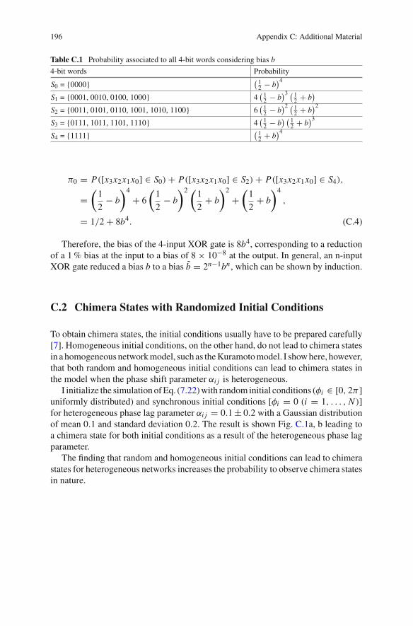
C.1 Bias Reduction of the XOR Operation
For the realization of a random number generator in Chap. 5, I use a 4-input XORgate to reduce bias and correlations. Here, I evaluate the resulting bias.
For the four inputs of theXORgate, I assume uncorrelated binary variables {xi }3i=0sampled from identically biased uniform distributions with a probability of a 0 or 1given by
P(xi = 0) = 1
2− b and P(xi = 1) = 1
2+ b. (C.1)
The resulting probabilities associated with 4-bit words with different counts of 1are calculated in Table C.1.
I compute the probability
π0 = P
(3⊕
i=0
xi = 0
)
, (C.2)
which can be used to calculate the bias b = |π0 − 0.5|.Equation (C.2) can be evaluated by considering the words leading to an output
of either 1 or 0. For this, I use that the XOR operation is the parity of the inputs.Therefore, words in S0, S2, and S4 in Table C.1 lead to a 0 output and hence
π0 = P ([x3x2x1x0] ∈ S0 ∪ [x3x2x1x0] ∈ S2 ∪ [x3x2x1x0] ∈ S4) . (C.3)
Assuming uncorrelated bitstreams, these three events are disjoint. Using values fromTable C.1, I calculate
© Springer International Publishing Switzerland 2015D.P. Rosin, Dynamics of Complex Autonomous Boolean Networks,Springer Theses, DOI 10.1007/978-3-319-13578-6
195
196 Appendix C: Additional Material
Table C.1 Probability associated to all 4-bit words considering bias b
4-bit words Probability
S0 = {0000}( 12 − b
)4
S1 = {0001, 0010, 0100, 1000} 4( 12 − b
)3 ( 12 + b
)
S2 = {0011, 0101, 0110, 1001, 1010, 1100} 6( 12 − b
)2 ( 12 + b
)2
S3 = {0111, 1011, 1101, 1110} 4( 12 − b
) ( 12 + b
)3
S4 = {1111}( 12 + b
)4
π0 = P([x3x2x1x0] ∈ S0) + P([x3x2x1x0] ∈ S2) + P([x3x2x1x0] ∈ S4),
=(1
2− b
)4
+ 6
(1
2− b
)2 (1
2+ b
)2
+(1
2+ b
)4
,
= 1/2 + 8b4. (C.4)
Therefore, the bias of the 4-input XOR gate is 8b4, corresponding to a reductionof a 1% bias at the input to a bias of 8 × 10⁻⁸ at the output. In general, an n-inputXOR gate reduced a bias b to a bias b = 2n−1bn , which can be shown by induction.
C.2 Chimera States with Randomized Initial Conditions
To obtain chimera states, the initial conditions usually have to be prepared carefully[7]. Homogeneous initial conditions, on the other hand, do not lead to chimera statesin a homogeneous networkmodel, such as theKuramotomodel. I showhere, however,that both random and homogeneous initial conditions can lead to chimera states inthe model when the phase shift parameter αi j is heterogeneous.
I initialize the simulationofEq. (7.22)with random initial conditions (φi ∈ [0, 2π ]uniformly distributed) and synchronous initial conditions [φi = 0 (i = 1, . . . , N )]for heterogeneous phase lag parameter αi j = 0.1± 0.2 with a Gaussian distributionof mean 0.1 and standard deviation 0.2. The result is shown Fig. C.1a, b leading toa chimera state for both initial conditions as a result of the heterogeneous phase lagparameter.
The finding that random and homogeneous initial conditions can lead to chimerastates for heterogeneous networks increases the probability to observe chimera statesin nature.

Appendix C: Additional Material 197
0 50 100 150
time (ms)
0
30
60
90
120
i
11
12
13
f (M
Hz)
0 50 100 150
time (ms)
0
30
60
90
120
i
11
12
13
f (M
Hz)
(a)
(b)
Fig. C.1 Numerical simulation of the Eq. (7.22) with heterogeneous αi, j . a Random initial condi-tions, b homogeneous initial conditions. The oscillator index is shifted so that the unsynchronizedregion of the chimera appears in the middle of the network. Other parameters as in Fig. 5 in themain article
C.3 Cluster Synchronization in Coupled Neural Populations
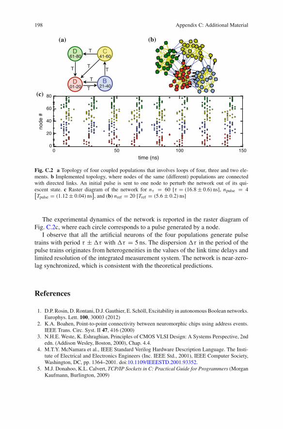
In this section, I study the dynamics of an artificial neural network of 80 excitablenodes. With this, I show that I can build large meta-networks of silicon neurons.2
I assemble Boolean neurons in a network of four distinct neural populations, asillustrated in Fig. C.2a, b. Dynamical properties of similar network topologies havebeen investigated theoretically [9, 10] because of their similarity to neural circuitssuch as the thalamic circuitry embedded in the brain [11, 12].
In the experiment, each population consists of 20 excitable nodes, totaling 80nodes for the entire network. Nodes within a population are connected with proba-bility p = 0.3, where links are realized with on-chip wires leading to small link timedelays. Nodes of different populations are connected with probability p = 0.015with time-delay links with τ = (16.8 ± 0.6) ns. These probabilities lead to strongconnections of nodes within a population with negligible link delay and loose con-nections between nodes of different populations with significant time delay τ .
The dynamics of the artificial neural network is described theoretically by Kanterand collaborators [13, 14]. According to the theory, the network dynamics is givenby the network topology of the community structure by the greatest common divisor(GCD) of the sizes of directed loops. In the network topology in Fig. C.2, inspiredby Fig. 1a in Ref. [13], there are three directed loops of two, three, and four neuralpopulations, respectively. Therefore, the theory predicts a number of synchronizedzero-lag synchronized clusters of GCD(2, 3, 4) = 1, i.e., all the populations arepredicted to be synchronized with zero time lag (see also Sect. 9.3.2).
2 This study is published in Ref. [8].
198 Appendix C: Additional Material
D01-20
C41-60
B21-40
D61-80
0 50 100 150
time (ns)
0
20
40
60
80
node
#(a) (b)
(c)
T
TT
T
T
T
Fig. C.2 a Topology of four coupled populations that involves loops of four, three and two ele-ments. b Implemented topology, where nodes of the same (different) populations are connectedwith directed links. An initial pulse is sent to one node to perturb the network out of its qui-escent state. c Raster diagram of the network for nτ = 60 [τ = (16.8 ± 0.6) ns], npulse = 4[Tpulse = (1.12 ± 0.04) ns
], and (b) nref = 20 [Tref = (5.6 ± 0.2) ns]
The experimental dynamics of the network is reported in the raster diagram ofFig. C.2c, where each circle corresponds to a pulse generated by a node.
I observe that all the artificial neurons of the four populations generate pulsetrains with period τ ± �τ with �τ = 5 ns. The dispersion �τ in the period of thepulse trains originates from heterogeneities in the values of the link time delays andlimited resolution of the integrated measurement system. The network is near-zero-lag synchronized, which is consistent with the theoretical predictions.
References
1. D.P. Rosin, D. Rontani, D.J. Gauthier, E. Schöll, Excitability in autonomous Boolean networks.Europhys. Lett. 100, 30003 (2012)
2. K.A. Boahen, Point-to-point connectivity between neuromorphic chips using address events.IEEE Trans. Circ. Syst. II 47, 416 (2000)
3. N.H.E. Weste, K. Eshraghian, Principles of CMOS VLSI Design: A Systems Perspective, 2ndedn. (Addison Wesley, Boston, 2000), Chap. 4.4.
4. M.T.Y. McNamara et al., IEEE Standard Verilog Hardware Description Language. The Insti-tute of Electrical and Electronics Engineers (Inc. IEEE Std., 2001), IEEE Computer Society,Washington, DC, pp. 1364–2001. doi:10.1109/IEEESTD.2001.93352.
5. M.J. Donahoo, K.L. Calvert, TCP/IP Sockets in C: Practical Guide for Programmers (MorganKaufmann, Burlington, 2009)
Appendix C: Additional Material 199
6. W.H. Press, Numerical Recipes 3rd Edition: The Art of Scientific Computing (CambridgeUniversity Press, Cambridge, 2007)
7. D.M.Abrams, S.H. Strogatz, Chimera states for coupled oscillators. Phys. Rev. Lett. 93, 174102(2004)
8. D.P. Rosin, D. Rontani, D.J. Gauthier, E. Schöll, Experiments on autonomous Boolean net-works. Chaos 23, 025102 (2013)
9. R. Vicente, L.L. Gollo, C.R. Mirasso, I. Fischer, P. Gordon, Dynamical relaying can yield zerotime lag neuronal synchrony despite long conduction delays. Proc. Natl. Acad. Sci. USA 105,17157 (2008)
10. E. Kopelowitz, M. Abeles, D. Cohen, I. Kanter, Sensitivity of global network dynamics to localparameters versus motif structure in a cortexlike neuronal model. Phys. Rev. E 85, 051902(2012)
11. E.G. Jones, Thalamic circuitry and thalamocortical synchrony. Phil. Trans. R. Soc. B 357, 1659(2002)
12. S. Shipp, The functional logic of cortico-pulvinar connections. Phil. Trans. R. Soc. B 358, 1605(2003)
13. I. Kanter, E. Kopelowitz, R. Vardi, M. Zigzag, W. Kinzel, M. Abeles, D. Cohen, Nonlocalmechanism for cluster synchronization in neural circuits. Europhys. Lett. 93, 66001 (2011)
14. R. Vardi, A. Wallach, E. Kopelowitz, M. Abeles, S. Marom, I. Kanter, Synthetic reverberatingactivity patterns embedded in networks of cortical neurons. Europhys. Lett. 97, 066002 (2012)


![High Performance Logic Style with Constant Delay ... · traditional static and pass transistor CMOS logic ... domino (NORA domino) [3], zipper ... trendy logic style in high-performance](https://img.pdfslide.net/doc/110x75/5b7b4e627f8b9adb4c8c5a93/high-performance-logic-style-with-constant-delay-traditional-static-and.jpg)