Embed Size (px)
Citation preview
APPENDIX D SIMCHECK II OWNER’S MANUAL
PAGE 116
APPENDIX D:
EDO/FPM TIMING MEASUREMENTS
The most important parameter of a memory chip is its speedcapability, which is characterized by its Access Time. The AccessTime is the dominant factor in the cost of memory chips andmodules. It is also the only parameter which is marked on the chips.
The primary function of a memory chip is to retrieve and to storedata. Ideally, it would be very desirable if a memory chip coulddeliver its stored data at the exact instant of time when it receivesthe read command. In practice, this process does take some lengthof time which is generally called Access Time. Intuitively, theAccess Time of a memory chip is the length of time from themoment the chip is instructed to read specific data until the point intime when the required data is available at the chip's output.
DRAM chips utilize a clever accessing scheme which allows them toaddress 16,000,000 cells (which require 24 address bits) by scanningthe address bits in two portions (ROW and COLUMN). As a result,a 16M chip can use only 12 pins for the address bits. To load theaddress, two control signals, RAS (Row Address Scan) and CAS(Column Address Scan), are applied sequentially to the chip. Theperiod of time between the initiation of the RAS signal until theinstant when the data is available at the chip's output is called theDRAM Access Time. The Access Time determines the speed of amemory chip: A chip with a shorter Access Time is faster.
The chip manufacturer marks (and rates) chips with the WORSTCASE condition. In other words, the manufacturer fully guaranteesthat the chip Access Time will either meet or exceed its markedrating under full recommended operating conditions. The industrystandard "recommended operating conditions" means operating
voltages from 4.5V to 5.5V, temperature from 0oC to 70oC,maximum capacitance load on the data-line of 100pF, and maximumdata-line load of 2 TTL input loads.
SIMCHECK II measures the ACTUAL Access Time of the chip asit is subjected to the maximum recommended loading condition andunder the lowest voltage within the chip specifications.
You will be surprised to see that in most cases the ACTUAL Access
SIMCHECK II OWNER’S MANUAL APPENDIX D
PAGE 117
Time is much better than the manufacturer's rating because mostmanufacturers tend to have a substantial margin of safety. However,as the DRAM technology matures (namely, chips with fasterratings), the difference between the manufacturer's rating and theACTUAL Access Time becomes smaller: a typical 150nS rated chipmay have 100nS ACTUAL Access Time at room temperature, whilean 80nS rated chip may have 70nS ACTUAL Access Time at roomtemperature.
While SIMCHECK II helps you to sort out faster memory modulesin comparison to their marked WORST-CASE Access Time, careshould be taken along the following general guidelines:
1. Memory chips become slower at higher temperatures - the
same chip which can run at 54nS at 25oC may slow down to
68nS at 70oC. Therefore, the BASIC SIMCHECK II testwhich is conducted at room temperature may show a betterAccess Time than the later EXTENSIVE test that includes theChip-Heat mode, where the module will actually be warmedto true working temperatures.
2. Memory chips become slower at lower voltages - the samechip which can run at 90nS at 5.5V may slow down to 100nSat 4.5V. Therefore, SIMCHECK II's Access Time tests areconducted at 4.5V for 5.0V devices and at 3.0V for 3.3Vdevices.
3. Other speed related factors (e.g. loading conditions) may bedifferent in your particular application as compared to thetesting conditions.
After obtaining the speed of the memory module from yourSIMCHECK II, determine your own margin of speed-variation andbase it on the above arguments and your particular application.Experiment with modules of different actual Access Times todetermine your margin of safety. We would like to emphasize thatSIMCHECK II provides you with the ACTUAL Access Timereading, with no added artificial margin.
With SIMCHECK II, the actual Access Time is automaticallycalculated and displayed. There is no need to set an Access Timeswitch. The module's Access Time is determined by the slowestchip on the module and our SINGLE BIT test will also show youthe speed of each chip on the module! Additionally, the Chip-Heatmode warms the module to actual working temperatures, an
APPENDIX D SIMCHECK II OWNER’S MANUAL
PAGE 118
important parameter in Access Time measurement.
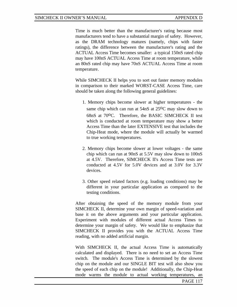
Cycle Time Measurement
One of the unique achievements of SIMCHECK II is the ability totest the cycle time of the memory device. It is important tounderstand the difference between a module’s cycle time and itsaccess time. The access time of a memory device is the minimumtime delay between the initiation of the access operation and thetime when the accessed data is available at the device output port.The access time is the timing parameter marked on the memory chipand is readily tested by SIMCHECK II. The cycle time of thememory device is the minimum time delay from one memory accessto the next. Therefore, the shorter the cycle time, the more dataaccesses can be performed each second (higher data rate). Aftereach access, the DRAM device needs a time-out period (called aprecharge time). This precharge time significantly slows down thecycle time of DRAM devices compared to SRAM devices, andtherefore becomes a speed limiting factor in DRAM operation.SIMCHECK II’s ability to test cycle time is an important feature notpreviously available on comparable testers. This enhances theusefulness of SIMCHECK II in determining the quality and actualoperational speed of the tested memory devices.
APPENDIX E
PAGE 119
APPENDIX E:
MODULE REPAIR WITH SIMCHECK II
SIMCHECK II is not merely a Pass/Fail tester. It is designed toprovide you with explicit error data to enable you to identify thedefective component/s on the DUT.
The SIMCHECK II test starts first by checking the external wiringof the DUT, then it quickly determines the structure and speed ofthe DUT and identifies internal wiring problems, DRAM modes(e.g. EDO), and any defective DRAM interface circuitry. After thisset of quick tests, the entire memory array is thoroughly examined.
You will find the following features to be useful in your repairefforts:
1. The Test Log: All the test results, structure/speed information anddetected errors are reported on the screen and immediately storedin the Test Log. The Test Log is accessed from STANDBYmode by pressing F4 and it contains all the information from thelast test. Upon exiting the Test Log, all error menus are re-created, allowing you to extract any information you may havemissed during the actual test. Even if the test is prematurelyterminated once an error is detected, you can still find valuableinformation in the Test Log.
2. Continuation After Error: SIMCHECK II does not stop when itencounter errors, unless the error is FATAL in nature (like“RAS0 stuck at 0” which will terminate the test as you cannotaccess the DUT). You can continue to test after most errormessages by pressing F1. This gives you more information ascan be shown in the following example. Suppose SIMCHECK IIfirst halts the test with an address error. If you continue the test,a bit data error may further indicate which chip/s caused the error(unless, of course, the address error is due to a connectorproblem common to all the chips).
3. Advanced Setup: You may also use the advanced setup featuresoutlined in Section 6 to further analyze the errors. Such setupfeatures allow you, for example, to test only part of the DUT(setup size), or you can fix the speed at much slower values.You can also check the device at specific values for Trcd, Trah,
APPENDIX E SIMCHECK II OWNER’S MANUAL
PAGE 120
and other parameters.
4. SINGLE BIT Test: SIMCHECK II’s SINGLE BIT test has beensignificantly upgraded from our previous models, and it is nowdesigned to give you much more information while concentratingexplicitly on each bit. You can also access the SINGLE BIT testdirectly from STANDBY mode, enabling some investigation ofthose devices with fatal errors. This test is not used on SDRAMtesting.
SIMCHECK II’s errors generally identify the relevant pins (circuitconnections to the test socket) of the DUT which are associatedwith the problem. You can remove the DUT from the socket andreview the Test Log, which is kept in SIMCHECK II’s ownmemory, until you start another test.
Only a technician with component-level repair expertise can repair amemory module. The required soldering/desoldering equipment isrelatively complex, especially with modules and cards made withextremely thin Surface Mount technology (TSOP). Nevertheless, afew minor problems which are identified by SIMCHECK II can berepaired with simple tools. A short between an adjacent pin may becaused by a small piece of metallic debris which is stuck betweentwo chips. You "repair" the module in this case with an Exactoknife or a watchmaker's fine screwdriver by simply removing thedebris.
If you use SIMCHECK II in the production shop, you should beable to easily replace the DUT’s components. You will need toconvert SIMCHECK II’s error notifications from pin numbers to theactual parts on your DUT.
When working with 72-pin SIMM modules or 168-pin DIMMs, youwill need to have a wiring diagram of the module to identify the chipwhich is connected to the data line (DQ pin) which was identified asbad by SIMCHECK II. We have included some tables of JEDECpin numbers in Appendix E. Module wiring diagrams and DRAMchip data sheets are available from their manufacturers.
If you do not have the actual wiring for the DUT, do not despair.With hundreds of DUT board designs available, wiring diagrams arehard to find. You can, however, use a continuity meter from the pinidentified by SIMCHECK II to find the connected chip. Please notethat with data (DQ) type error, you can identify the actual defectivechip, taking care to work on the DUT’s BANK (B1, B2, etc.)
SIMCHECK II OWNER’S MANUAL APPENDIX E
PAGE 121
identified by SIMCHECK II. If the problem is with address linesthat are common to all chips, you may need to run more tests (pressF1 to Continue when the address error is first reported) or use theSINGLE BIT test to find a relation between the address lineproblem and a particular chip. Of course, if the address line problemis on the trace to the DUT’s connector, the address error is commonto all chips.
If you work with the older 30 pin SIMMs, identification is typicallyeasier. For example, if the module is made up of 8 or 9 chips, bit 1is in the chip closest to pin 1 of the module. Bit 2 is the second chipand so forth. If the module is made with three chips, then bits 1 to 4are in the left chip (the one closest to pin 1), and bits 5 to 8 are inthe middle chip. Bit 9 is in the furthest right chip.
APPENDIX F SIMCHECK II OWNER’S MANUAL
PAGE 122
APPENDIX F:
MEMORY MODULE TECHNICAL REVIEWThroughout the computer era, the need for faster and densermemory devices has put constant pressure on memorymanufacturers. The push to maximize memory capabilities hasresulted in ever-changing technology.
The Evolution of the DIMM Module
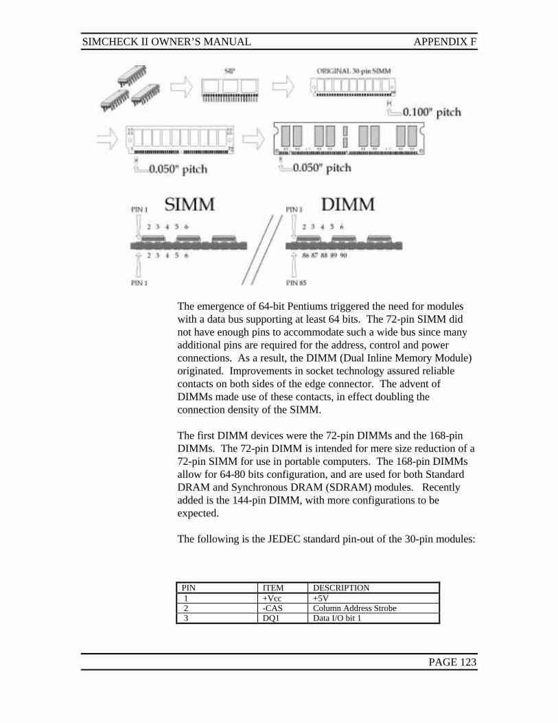
In the early and mid-80s, memory modules were made in a variety ofpinouts and without any dominant standards. Early PCs usedindividual DRAM chips on the motherboard. An early module, theTM4164EQ5 had five such chips on a 24-pin module to achieve a64Kx5 module.
The first 22-pin SIP (Single Inline Package) modules appeared in theearly 80s, comprised of memory devices mounted on a PCB with 22interconnection pins spaced at 0.100” intervals along a line.Memory modules became popular only after the Wang Laboratoriesinvention of the SIMM (Single Inline Memory Module) technology,where the SIP’s legs have been replaced by an edge connector and aconvenient mounting feature which includes a special tab to identifypin 1 and two mounting holes.
By the early 90s, most computer systems switched to the SIMMtechnology due to greater space saving capabilities. OriginalSIMMs had 30 contacts (pins) which were spaced apart at 0.100”.Although contacts for the SIMM device appear on both sides of theedge connector, all opposite contacts are shorted together across theboard to achieve more reliable contact with the SIMM socket (seeillustration). With the 30-pin limited to 16Mx9, IBM extended theSIMM pin count to 72 for their PS/2 computers, thus allowing formodules with 16Mx36 or x40 bits. To make the PS/2 SIMM modulesmall, the spacing between the contacts was halved to 0.050”, butopposite contacts were still shorted across the edge connector.
All solid state memory configurations are now coordinated andstandardized by the Electronic Industries Association through itsJEDEC Standard 21-C.
SIMCHECK II OWNER’S MANUAL APPENDIX F
PAGE 123
The emergence of 64-bit Pentiums triggered the need for moduleswith a data bus supporting at least 64 bits. The 72-pin SIMM didnot have enough pins to accommodate such a wide bus since manyadditional pins are required for the address, control and powerconnections. As a result, the DIMM (Dual Inline Memory Module)originated. Improvements in socket technology assured reliablecontacts on both sides of the edge connector. The advent ofDIMMs made use of these contacts, in effect doubling theconnection density of the SIMM.
The first DIMM devices were the 72-pin DIMMs and the 168-pinDIMMs. The 72-pin DIMM is intended for mere size reduction of a72-pin SIMM for use in portable computers. The 168-pin DIMMsallow for 64-80 bits configuration, and are used for both StandardDRAM and Synchronous DRAM (SDRAM) modules. Recentlyadded is the 144-pin DIMM, with more configurations to beexpected.
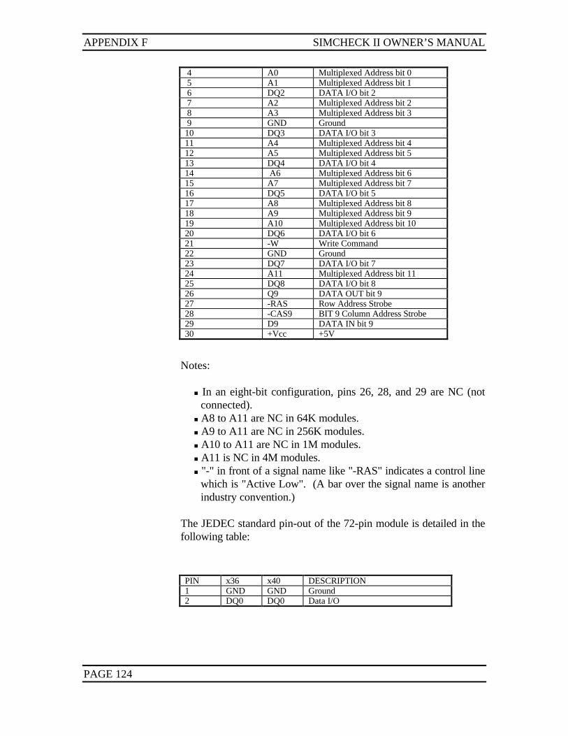
The following is the JEDEC standard pin-out of the 30-pin modules:
PIN ITEM DESCRIPTION 1 +Vcc +5V 2 -CAS Column Address Strobe 3 DQ1 Data I/O bit 1
APPENDIX F SIMCHECK II OWNER’S MANUAL
PAGE 124
4 A0 Multiplexed Address bit 0 5 A1 Multiplexed Address bit 1 6 DQ2 DATA I/O bit 2 7 A2 Multiplexed Address bit 2 8 A3 Multiplexed Address bit 3 9 GND Ground10 DQ3 DATA I/O bit 311 A4 Multiplexed Address bit 412 A5 Multiplexed Address bit 513 DQ4 DATA I/O bit 414 A6 Multiplexed Address bit 615 A7 Multiplexed Address bit 716 DQ5 DATA I/O bit 517 A8 Multiplexed Address bit 818 A9 Multiplexed Address bit 919 A10 Multiplexed Address bit 1020 DQ6 DATA I/O bit 621 -W Write Command22 GND Ground23 DQ7 DATA I/O bit 724 A11 Multiplexed Address bit 1125 DQ8 DATA I/O bit 826 Q9 DATA OUT bit 927 -RAS Row Address Strobe28 -CAS9 BIT 9 Column Address Strobe29 D9 DATA IN bit 930 +Vcc +5V
Notes:
n In an eight-bit configuration, pins 26, 28, and 29 are NC (notconnected).
n A8 to A11 are NC in 64K modules.n A9 to A11 are NC in 256K modules.n A10 to A11 are NC in 1M modules.n A11 is NC in 4M modules.n "-" in front of a signal name like "-RAS" indicates a control line
which is "Active Low". (A bar over the signal name is anotherindustry convention.)
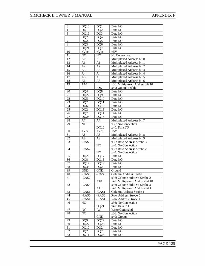
The JEDEC standard pin-out of the 72-pin module is detailed in thefollowing table:
PIN x36 x40 DESCRIPTION1 GND GND Ground2 DQ0 DQ0 Data I/O
SIMCHECK II OWNER’S MANUAL APPENDIX F
PAGE 125
3 DQ18 DQ1 Data I/O4 DQ1 DQ2 Data I/O5 DQ19 DQ3 Data I/O6 DQ2 DQ4 Data I/O7 DQ20 DQ5 Data I/O8 DQ3 DQ6 Data I/O9 DQ21 DQ7 Data I/O10 +Vcc +Vcc +5V11 NC NC No Connection12 A0 A0 Multiplexed Address bit 013 A1 A1 Multiplexed Address bit 114 A2 A2 Multiplexed Address bit 215 A3 A3 Multiplexed Address bit 316 A4 A4 Multiplexed Address bit 417 A5 A5 Multiplexed Address bit 518 A6 A6 Multiplexed Address bit 619 A10
-OEx36: Multiplexed Address bit 10x40: Output Enable
20 DQ4 DQ8 Data I/O21 DQ22 DQ9 Data I/O22 DQ5 DQ10 Data I/O23 DQ23 DQ11 Data I/O24 DQ6 DQ12 Data I/O25 DQ24 DQ13 Data I/O26 DQ7 DQ14 Data I/O27 DQ25 DQ15 Data I/O28 A7 A7 Multiplexed Address bit 729 NC
DQ16x36: No Connectionx40: Data I/O
30 +Vcc +Vcc +5V31 A8 A8 Multiplexed Address bit 832 A9 A9 Multiplexed Address bit 933 -RAS3
NCx36: Row Address Strobe 3x40: No Connection
34 -RAS2NC
x36: Row Address Strobe 2x40: No Connection
35 DQ26 DQ17 Data I/O36 DQ8 DQ18 Data I/O37 DQ17 DQ19 Data I/O38 DQ35 DQ20 Data I/O39 GND GND Ground40 -CAS0 -CAS0 Column Address Strobe 041 -CAS2
A10x36: Column Address Strobe 2x40: Multiplexed Address bit 10
42 -CAS3A11
x36: Column Address Strobe 3x40: Multiplexed Address bit 11
43 -CAS1 -CAS1 Column Address Strobe 144 -RAS0 -RAS0 Row Address Strobe 045 -RAS1 -RAS1 Row Address Strobe 146 NC
DQ21x36: No Connectionx40: Data I/O
47 -W -W Write Command48 NC
GNDx36: No Connectionx40: Ground
49 DQ9 DQ22 Data I/O50 DQ27 DQ23 Data I/O51 DQ10 DQ24 Data I/O52 DQ28 DQ25 Data I/O53 DQ11 DQ26 Data I/O
APPENDIX F SIMCHECK II OWNER’S MANUAL
PAGE 126
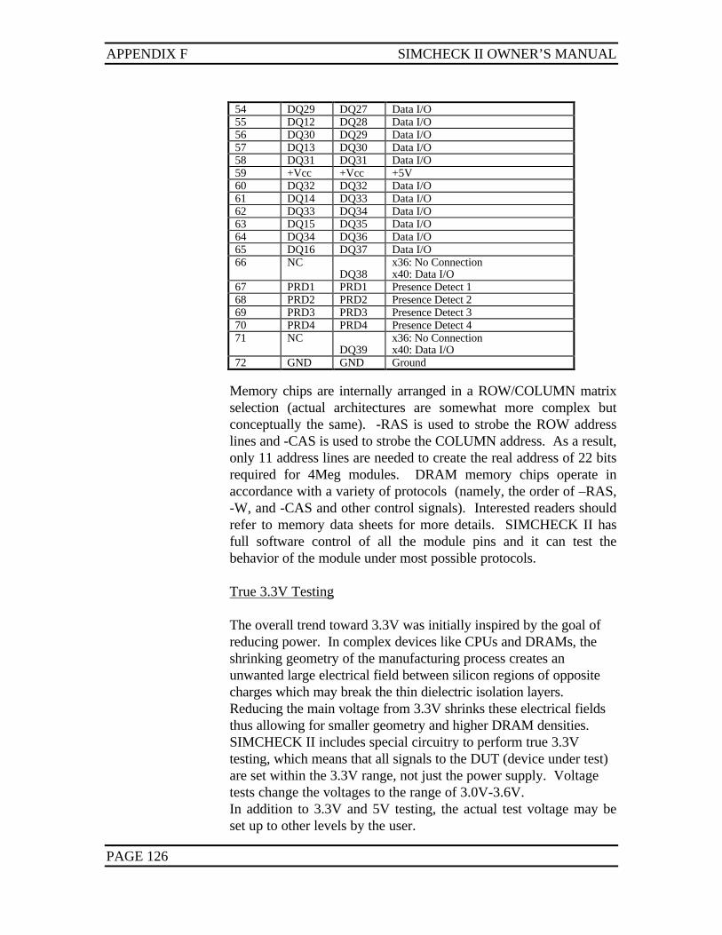
54 DQ29 DQ27 Data I/O55 DQ12 DQ28 Data I/O56 DQ30 DQ29 Data I/O57 DQ13 DQ30 Data I/O58 DQ31 DQ31 Data I/O59 +Vcc +Vcc +5V60 DQ32 DQ32 Data I/O61 DQ14 DQ33 Data I/O62 DQ33 DQ34 Data I/O63 DQ15 DQ35 Data I/O64 DQ34 DQ36 Data I/O65 DQ16 DQ37 Data I/O66 NC
DQ38x36: No Connectionx40: Data I/O
67 PRD1 PRD1 Presence Detect 168 PRD2 PRD2 Presence Detect 269 PRD3 PRD3 Presence Detect 370 PRD4 PRD4 Presence Detect 471 NC
DQ39x36: No Connectionx40: Data I/O
72 GND GND Ground
Memory chips are internally arranged in a ROW/COLUMN matrixselection (actual architectures are somewhat more complex butconceptually the same). -RAS is used to strobe the ROW addresslines and -CAS is used to strobe the COLUMN address. As a result,only 11 address lines are needed to create the real address of 22 bitsrequired for 4Meg modules. DRAM memory chips operate inaccordance with a variety of protocols (namely, the order of –RAS,-W, and -CAS and other control signals). Interested readers shouldrefer to memory data sheets for more details. SIMCHECK II hasfull software control of all the module pins and it can test thebehavior of the module under most possible protocols.
True 3.3V Testing
The overall trend toward 3.3V was initially inspired by the goal ofreducing power. In complex devices like CPUs and DRAMs, theshrinking geometry of the manufacturing process creates anunwanted large electrical field between silicon regions of oppositecharges which may break the thin dielectric isolation layers.Reducing the main voltage from 3.3V shrinks these electrical fieldsthus allowing for smaller geometry and higher DRAM densities.SIMCHECK II includes special circuitry to perform true 3.3Vtesting, which means that all signals to the DUT (device under test)are set within the 3.3V range, not just the power supply. Voltagetests change the voltages to the range of 3.0V-3.6V.In addition to 3.3V and 5V testing, the actual test voltage may beset up to other levels by the user.
SIMCHECK II OWNER’S MANUAL APPENDIX G
PAGE 127
APPENDIX G:
SIMCHECK II EXPANSION PORT
SIMCHECK II's design allows ample room for expansion andenhancement using its 40-Bit Expansion Port (behind the 72-pinSIMM socket) and its 96-pin DIN side socket. In addition tostandard adapters, we design customized adapters for customer'sproprietary modules. Alternatively, we can also support customersin their in-house development of their own special adapters.
This appendix presents some introductory information onSIMCHECK II's expansion. Please contact us for more detailedexamination of your specific requirements.
The SIMCHECK II’sExpansion Ports aswell as its entiredesign is a protectedintellectual propertyof INNOVENTIONSInc. Informationgiven in this section isintended forcustomers buildingtheir own in-houseadapters to use inconjunction withSIMCHECK II.
The most effective way to design a customized adapter for testingnon- standard memory devices is to connect the adapter directly tothe 40-Bit Expansion Port. This socket has 40 data lines (DQtype), 16 address lines, 4 RAS lines, 4 CAS lines, two write lines,four PRD lines, numerous power lines, and several special purposelines.
Our DIMMCHECK 168P option adapter (p/n INN-8484-9) is agood example illustrating how we have used this port to testDIMMs with up to 80 data lines, 8 CAS lines, 2 Id lines and 8 PRDlines.
Our CUSTOMIZED ADAPTER (p/n INN-8484-1) can serve as abasic breadboard for the development of your own adapters.
The SIMCHECK II 40-Bit Expansion Port is a 45x2 DINconnector. The following is the pin list of this proprietary busexpansion slot.Pin numbering: The bottom-left pin is pin 1. Pin 2 is the top-left pin.Numbering continues in a zigzag fashion across the connector. Pin89 is the bottom-right pin, and pin 90 is the top-right pin.
APPENDIX G SIMCHECK II OWNER’S MANUAL
PAGE 128
Pin # Function Pin # Function Pin#
Function
1 +5V 31 DQ22 61 DQ92 -W1 32 DQ7 62 DQ283 SEL1 33 DQ23 63 DQ104 VDD2 34 MA7 64 DQ295 MA12 35 MA11/DQ16 65 DQ116 MA13 36 VDD main 66 DQ307 GND 37 MA8 67 DQ128 DQ0 38 MA9 68 DQ319 DQ16 39 -RAS3 69 VDD main10 DQ1 40 -RAS2 70 DQ3211 DQ17 41 MDQ26 71 DQ1312 DQ2 42 MDQ8 72 DQ3313 DQ18 43 GND 73 DQ1414 DQ3 44 VDD main 74 DQ3415 DQ19 45 GND 75 DQ1516 VDD main 46 VDD main 76 MDQ3817 -CASP 47 MDQ17 77 PRD118 MA0 48 MDQ35 78 PRD219 MA1 49 GND 79 PRD320 MA2 50 -CAS0 80 PRD421 MA3 51 -CAS2/A10 81 MDQ3922 MA4 52 -CAS3/A11 82 GND23 MA5 53 -CAS1 83 SEL224 MA6 54 -RAS0 84 MA1025 MA10/OE 55 -RAS1 85 MA1526 DQ4 56 MDQ21 86 MA1127 DQ20 57 -W0 87 MA1428 DQ5 58 ECC 88 SEL329 DQ21 59 DQ8 89 SEL430 DQ6 60 DQ27 90 +5V
NOTES:
n This port is upward compatible with the SIMCHECK 40-BITPORT. Not all the signals are the same.
n MDQ lines are multiplexed with additional functions.
n Do not connect VDD2 (pin 4) to any of the other VDD mainlines.
n SEL1-4 are software controlled and may not be used incustomized adapters that will not require programmodification.
n Some lines (e.g. MA10, 11) are duplicated on purpose toavoid shared lines.
SIMCHECK II OWNER’S MANUAL APPENDIX H
PAGE 129
APPENDIX H:
SIMCHECK II MAINTENANCE
Please calibrateperiodically.Factorycalibration atregular intervalskeeps your unitcurrent to existingspecifications.
H.1 CALIBRATION & UPGRADE
Although system calibration is not an absolute requirement forSIMCHECK II/IIse PLUS, we do strongly recommend that youhave your unit serviced periodically. This makes sure that it remainscurrent to factory production specifications and operates at its mostoptimum level, thereby protecting your investment and ensuring thatyour test system does not become obsolete.
We recommend that each unit undergo a factory calibration &upgrade every 12-18 months. Additional information regardingwhat the upgrade covers can be obtained by visiting our website.
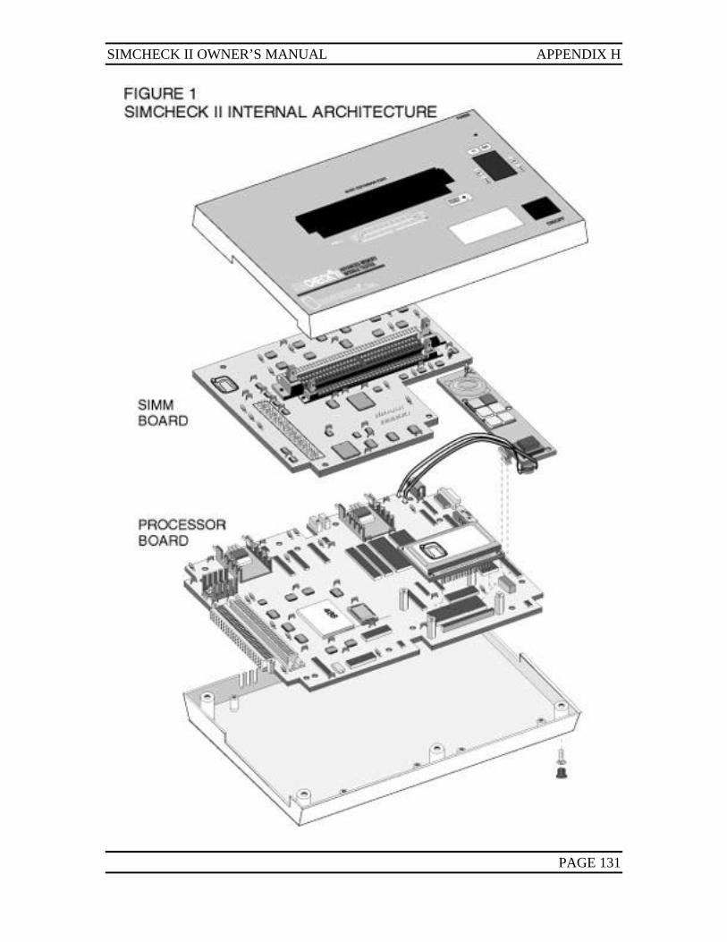
H.2 SIMCHECK II INTERNAL ARCHITECTURE
Referring to Figure 1, SIMCHECK II is made up of two PCBsjoined together through a 96-pin connector. SIMCHECK II can beopened by removing the six anti-skid rubber feet, then removing thesix corresponding phillips screws from the bottom of the enclosure.Once these screws are removed, you can simply lift up the top shell,as shown in Figure 1. The SIMCHECK II keyboard and the128x32-pixel LCD board are attached to the lower PCB (alsoknown as the Processor Board) using solderless connectors andscrews. The top board, known as the SIMM Board, can bedetached at the 96-pin connector.
H.3 Replacement of 30 or 72 pin sockets
The sockets used by SIMCHECK II are attached to the internalPCB with the use of solderless pin receptacles, or barrel sockets.Therefore, socket replacement is almost effortless, as no desolderingis required.
Socket Removal
1. Referring to Figure 1, remove the (6) anti-skid rubber feet, thenthe screws (#4x3/8 machine phillips).
2. Separate the case halves to expose the circuit boards.
APPENDIX H SIMCHECK II OWNER’S MANUAL
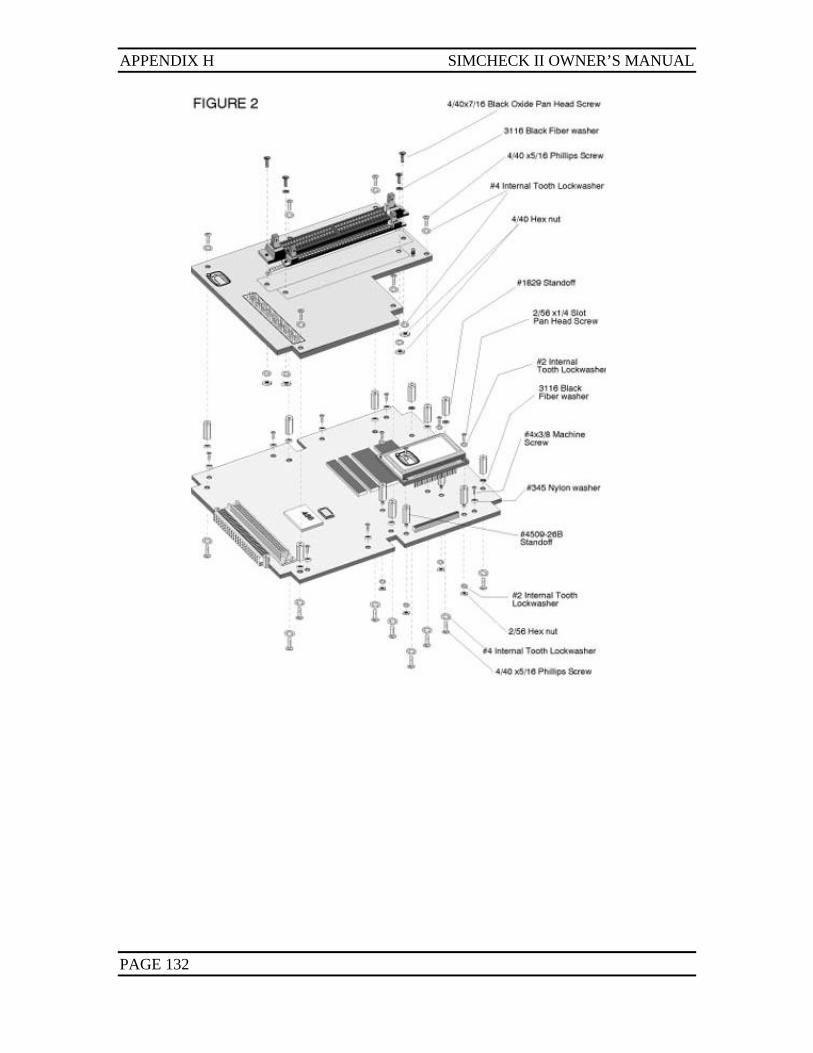
PAGE 130
3. Remove the (6) retaining screws (4/40 x 5/16 phillips) from thetop circuit board. Pull top circuit board straight up, separatingit from the bottom board as shown in Figure 2.
4. Remove the (2) screws (4/40 x 7/16 Black Oxide Pan Head)and black fiber washers.
5. Gently, using a rocking motion, pull to separate the socket fromthe circuit board.
Socket Insertion
1. Assure that there is no debris in the area where the new socketis to be placed.
2. Align the pins of the socket with the barrel sockets and gentlypush using a slight rocking motion.
3. Replace (2) screws (4/40 x 7/16 Black Oxide Pan Head) andfiber washers and tighten (Avoid damaging the circuit board byover tightening). See Figure 2.
4. Replace the top circuit board and replace (6) screws (4/40 x5/16 Phillips) and washers (do not over tighten).
5. Place the case halves back together and replace (6) screws (#4x 3/8 machine Phillips), do not over tighten. Replace the rubberfeet.
Refer to Section4.3 for additionalinformation onadjusting theLCD.
H.4 CHANGING JUMPER SETTINGS
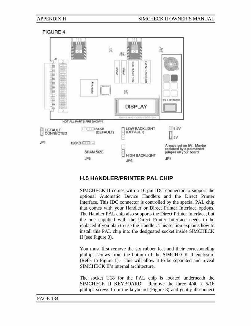
Figure 4 illustrates the jumpers on the SIMCHECK II’s processorboard. These jumpers are setup at the factory and you will rarelyneed to modify them. You will not need to change JP1 and P7 asthey are used for board testing only.JP6 controls the intensity of the LCD backlighting. It is set bydefault for LOW backlight, however, if you wish to switch to HIGHbacklight, you may set JP6 to the upper most settings.
JP5 controls the size of the SRAM chips installed in your board,which is currently 64KB SRAM. There may come a point whenSIMCHECK II’s SRAM chips will be upgraded to 128KB or256KB, which requires setting the JP5 jumper to the left.
SIMCHECK II OWNER’S MANUAL APPENDIX H
PAGE 131
APPENDIX H SIMCHECK II OWNER’S MANUAL
PAGE 132
SIMCHECK II OWNER’S MANUAL APPENDIX H
PAGE 133
APPENDIX H SIMCHECK II OWNER’S MANUAL
PAGE 134
H.5 HANDLER/PRINTER PAL CHIP
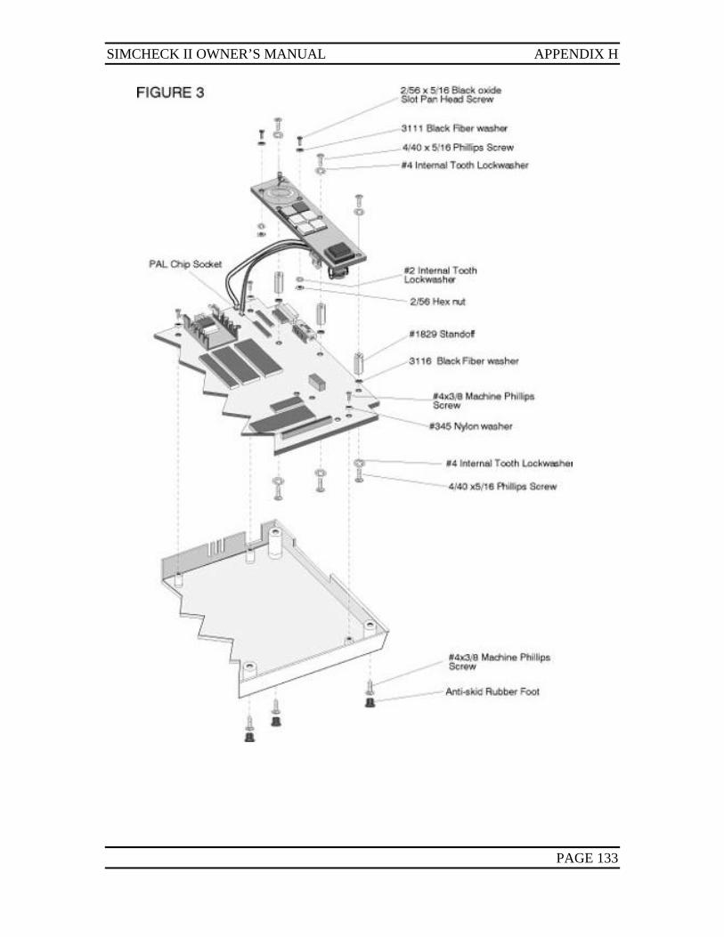
SIMCHECK II comes with a 16-pin IDC connector to support theoptional Automatic Device Handlers and the Direct PrinterInterface. This IDC connector is controlled by the special PAL chipthat comes with your Handler or Direct Printer Interface options.The Handler PAL chip also supports the Direct Printer Interface, butthe one supplied with the Direct Printer Interface needs to bereplaced if you plan to use the Handler. This section explains how toinstall this PAL chip into the designated socket inside SIMCHECKII (see Figure 3).
You must first remove the six rubber feet and their correspondingphillips screws from the bottom of the SIMCHECK II enclosure(Refer to Figure 1). This will allow it to be separated and revealSIMCHECK II’s internal architecture.
The socket U18 for the PAL chip is located underneath theSIMCHECK II KEYBOARD. Remove the three 4/40 x 5/16phillips screws from the keyboard (Figure 3) and gently disconnect
SIMCHECK II OWNER’S MANUAL APPENDIX H
PAGE 135
the keyboard from the Processor Board (the bottom PCB ofSIMCHECK II).
Install the special PAL chip that is enclosed with your SIMCHECKHANDLER companion into the empty socket marked U18 (SeeFigure 3) located just below the electrolytic capacitors on theProcessor Board.
Reconnect the keyboard to the Processor Board and secure it withthe three phillips screws. Close the SIMCHECK unit and test yourinstallation with your new Handler or Direct Printer Interface.
INDEX SIMCHECK II OWNER’S MANUAL
PAGE 136
INDEX
2200-PIN DIMM Adapter, 89
33.3V Testing, 96, 12630p module pinout, 123
772-pin modules, 96, 98, 124
AAccess Time, 5, 9, 34, 37, 55, 116
speed, 55, 116Activation Code Files, 69adapters, 5, 8, 12, 127, 128asymmetric refresh, 19Audible signals, 18, 21AUTO-LOOP test, 5, 9, 12, 27, 37, 39
BBank1, 31Bank2, 31BASIC test, 5, 9, 12, 19, 27, 30, 33, 34, 35, 36, 37,burn-in, 5, 39burst length, 46
CCALIBRATION & UPGRADE, 129Chip-Heat mode, 5, 37, 107, 116Continuation After Error, 119CUSTOMIZED Adapter, 98Cycle Time Measurement, 9, 116
DDEMO mode, 5, 8, 21DIMM, 63, 122, 123DIMMCHECK 144P PRO, 92DIMMCHECK 168P PRO, 91DIMMCHECK 72P PRO, 94DRAM CARD TESTER, 96DUT, 1, 9, 19
EECC, 33, 128
EDO, 5, 9, 36, 62, 119EDO/FPM Timing, 116error display. See menuserror list. See menuserror message, 19, 27, 30, 31, 41, 56EXTENSIVE test, 5, 9, 12, 27, 35, 36, 37, 41, 116
FFast Page Mode, 9, 31FINAL TEST, 9FIRMWARE, 2Firmware Files, 69FLASH EPROM, 5frequency setup, 58
Ggraphic display, 19, 30, 60graphic setup. See menusGroup1, 31Group2, 31
HHalting SINGLE BIT test, 41HANDLER, 101horizontal scroll menu, 22. See menus
IInternal Architecture, 129
JJEDEC Translation, 30, 96jumper settings, 130
Kkeyboard, 18, 21, 41
LLCD intensity, 21LED backlight, 21,130license agreement, 104
MMARCH UP/DOWN, 9menus, 5, 18, 19, 21, 22, 23, 24, 25, 31, 35, 41, 56,
57, 58, 60, 61, 62, 63, 64, 67, 68, 69, 119
SIMCHECK II OWNER’S MANUAL INDEX
PAGE 137
MODE Analysis, 9Mode Test, 36multipage list. See menus
NNIBBLE, 31non-standard 72-pin modules, 98
Ooptions, 80
Ppattern sensitivity, 36, 39, 107PC PROGRAMS, 68
Automated Firmware Upgrade, 71Communications Diagnostics, 79Graphics Communications, 78Realtime Interface, 72SIMCHECK II Downloader, 69SIMCHECK SETUP, 77SPD Support, 74Text Editor, 78
PC-100 Compliance, 46, 109PC-133 Compliance, 109power supply, 1, 8, 12, 37, 126precharge time, 116Printer Interface, 99Problem report form, 139Product Information Display, 15, 67Production Mode, 54
QQUICK INDEX, 80
RREADING SPD, 51Relative Refresh, 5, 9, 27, 37Relative Spikes, 5, 9
Sscreen display, 18SDRAM Timing, 109selection menu. See menussetup, 5, 18, 19, 22, 25, 27, 29, 55, 56, 57, 58, 60, 62SIMCHECK, 2, 80, 96, 101, 116, 126, 127SIMCHECK II se, 5, 12SIMCHECK II se Additions, 15SIMCHECK II se Program Module Upgrades, 15SIMCHECK II SE vs SIMCHECK II, 12SIMCHECK PLUS, 12SIMM, 96SINGLE BIT test, 5, 9, 12, 27, 36, 37, 39, 41, 119SIP Adapter, 100
socket rating, 26Socket replacement, 129sockets, 1, 2, 12, 26SPD EDITING AND FILING, 51SPD EEPROM, 84, 86SPD MANAGEMENT, 46, 82SPD Program Enable, 65SPD Programming
Enable SPD Programming, 53speed. See Access timeSPEED LIMIT, 58Speed Override, 34STANDBY mode, 8, 23, 29, 31, 35, 56, 119structure, 5, 9, 12, 19, 33, 119Sync CHIP TESTER, 27, 41, 80, 87Sync DIMMCHECK 100, 27, 85Sync DIMMCHECK 144, 83Sync DIMMCHECK 168, 81Sync DIMMCHECK Configuration, 66
TTac Access Times, 46, 109, 110Tcac Access Time, 36Technical Review, 122Temperature stress test. See Chip-Heat modetest algorithms, 107test flow, 5, 12, 62Test Log, 1, 12, 19, 23, 29, 31, 35, 36, 37, 39, 41,
119test modes, 27test results, 1, 3, 5, 12, 19, 25, 37, 39, 41, 119TEST SETUP mode, 56, 101time delay, 5, 19, 37, 116Troubleshooting, 102
Uuser interface, 18
Vvariable setup. See menusvertical scroll. See menusVoltage Bounce, 5, 9, 36, 107Voltage Cycling, 5, 9, 36, 107
WWarning Condition, 19warranty, 2Web site, 69
ZZIF. See Sockets