Embed Size (px)
Citation preview
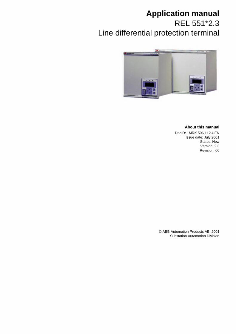
© ABB Automation Products AB 2001Substation Automation Division
Application manualREL 551*2.3
Line differential protection terminal
About this manualDocID: 1MRK 506 112-UEN
Issue date: July 2001Status: NewVersion: 2.3Revision: 00

COPYRIGHT
WE RESERVE ALL RIGHTS TO THIS DOCUMENT, EVEN IN THE EVENT THAT A PATENT IS ISSUED AND A DIFFERENT COMMERCIAL PROPRIETARY RIGHT IS REGISTERED. IMPROPER USE, IN PARTICULAR REPRODUCTION AND DIS-SEMINATION TO THIRD PARTIES, IS NOT PERMITTED.
THIS DOCUMENT HAS BEEN CAREFULLY CHECKED. IF THE USER NEVERTHELESS DETECTS ANY ERRORS, HE IS ASKED TO NOTIFY US AS SOON AS POSSIBLE.
THE DATA CONTAINED IN THIS MANUAL IS INTENDED SOLELY FOR THE PRODUCT DESCRIPTION AND IS NOT TO BE DEEMED TO BE A STATEMENT OF GUARANTEED PROPERTIES. IN THE INTERESTS OF OUR CUSTOMERS, WE CON-STANTLY SEEK TO ENSURE THAT OUR PRODUCTS ARE DEVELOPED TO THE LATEST TECHNOLOGICAL STAN-DARDS. AS A RESULT, IT IS POSSIBLE THAT THERE MAY BE SOME DIFFERENCES BETWEEN THE HW/SW PRODUCT AND THIS INFORMATION PRODUCT.
Manufacturer:
ABB Automation Products ABSubstation Automation DivisionSE-721 59 VästeråsSwedenTel: +46 (0) 21 34 20 00Fax: +46 (0) 21 14 69 18Internet: http://www.abb.se
Contents
PageChapter
Chapter 1 Introduction ..................................................................... 1
Introduction to the application manual ................................................. 2About the complete set of manuals to a terminal............................ 2Intended audience .......................................................................... 3Related documents......................................................................... 3Revision notes ................................................................................ 3
Chapter 2 General............................................................................. 5
Features............................................................................................... 6Application ........................................................................................... 7Design.................................................................................................. 8Requirements ...................................................................................... 9Terminal identification........................................................................ 16
Application .................................................................................... 16Calculations .................................................................................. 16
Chapter 3 Common functions ....................................................... 19
Time synchronisation (TIME)............................................................. 20Application .................................................................................... 20Functionality ................................................................................. 20Calculations .................................................................................. 20
Setting group selector (GRP)............................................................. 22Application .................................................................................... 22Functionality ................................................................................. 22Design .......................................................................................... 23
Setting lockout (HMI) ......................................................................... 24Application .................................................................................... 24Functionality ................................................................................. 24
I/O system configurator (IOP) ............................................................ 26Application .................................................................................... 26Functionality ................................................................................. 26
Logic function blocks ......................................................................... 30Application .................................................................................... 30Functionality ................................................................................. 30Calculations .................................................................................. 44
Self supervision (INT) ........................................................................ 46Application .................................................................................... 46Functionality ................................................................................. 47
Blocking of signals during test ........................................................... 50Functionality ................................................................................. 50
Contents
Chapter 4 Line differential.............................................................. 53
Line differential protection (DIFL)....................................................... 54Application .................................................................................... 54Functionality.................................................................................. 55Design........................................................................................... 58Calculations .................................................................................. 70
Chapter 5 Current ........................................................................... 73
Instantaneous overcurrent protection (IOC)....................................... 74Application .................................................................................... 74Functionality.................................................................................. 75Design........................................................................................... 75Calculations .................................................................................. 79
Time delayed overcurrent protection (TOC) ...................................... 89Application .................................................................................... 89Functionality.................................................................................. 89Design........................................................................................... 90Calculations .................................................................................. 93
Two step time delayed phase overcurrent protection (TOC2) ........... 97Application .................................................................................... 97Functionality.................................................................................. 97Calculations .................................................................................. 98
Definite and inverse time-delayed residual overcurrent protection (TEF) ........................................................... 103
Application .................................................................................. 103Functionality................................................................................ 104Calculations ................................................................................ 106
Thermal overload protection (THOL) ............................................... 110Application .................................................................................. 110Functionality................................................................................ 110Calculations ................................................................................ 111
Breaker failure protection (BFP) ...................................................... 114Application .................................................................................. 114Functionality................................................................................ 116Design......................................................................................... 120Calculations ................................................................................ 121
Unbalance protection for capacitor banks (TOCC) .......................... 123Application .................................................................................. 123Functionality................................................................................ 123Calculations ................................................................................ 124
Chapter 6 Power system supervision ......................................... 125
Broken conductor check (BRC) ....................................................... 126Application .................................................................................. 126Functionality................................................................................ 126Design......................................................................................... 126
Contents
Calculations ................................................................................ 127Overload supervision (OVLD).......................................................... 130
Application .................................................................................. 130Functionality ............................................................................... 130Design ........................................................................................ 130Calculations ................................................................................ 131
Chapter 7 Secondary system supervision ................................. 133
Current circuit supervision (CTSU) .................................................. 134Application .................................................................................. 134Functionality ............................................................................... 134Calculations ................................................................................ 136
Chapter 8 Control ......................................................................... 137
Automatic reclosing function (AR) ................................................... 138Application .................................................................................. 138Functionality ............................................................................... 140Calculations ................................................................................ 146
Single command (CD) ..................................................................... 153Application .................................................................................. 153Design ........................................................................................ 154Calculations ................................................................................ 155
Multiple command (CM)................................................................... 156Application .................................................................................. 156Design ........................................................................................ 156Calculations ................................................................................ 157
Chapter 9 Logic............................................................................. 159
Trip logic (TR) .................................................................................. 160Application .................................................................................. 160Functionality ............................................................................... 161Design ........................................................................................ 162
Pole discordance protection (PD) .................................................... 168Application .................................................................................. 168Functionality ............................................................................... 168Design ........................................................................................ 169Calculations ................................................................................ 171
Communication channel logic (CCHL)............................................. 172Application .................................................................................. 172Functionality ............................................................................... 172Calculations ................................................................................ 175
Communication channel test logic (CCHT)...................................... 176Application .................................................................................. 176Design ........................................................................................ 176
Event function (EV).......................................................................... 179
Contents
Application .................................................................................. 179Functionality................................................................................ 179Design......................................................................................... 179Calculations ................................................................................ 181
Event counter (CN) .......................................................................... 183Application .................................................................................. 183Functionality................................................................................ 183Calculations ................................................................................ 184
Chapter 10 Monitoring.................................................................... 185
LED indication function (HL, HLED)................................................. 186Application .................................................................................. 186Functionality................................................................................ 186Calculations ................................................................................ 199
Disturbance report (DRP) ................................................................ 200Application .................................................................................. 200Functionality................................................................................ 200Calculations ................................................................................ 205
Indications........................................................................................ 212Application .................................................................................. 212Functionality................................................................................ 212Calculations ................................................................................ 213
Disturbance recorder ....................................................................... 214Application .................................................................................. 214Functionality................................................................................ 214Design......................................................................................... 217Calculations ................................................................................ 218
Event recorder ................................................................................. 220Application .................................................................................. 220Functionality................................................................................ 220Calculations ................................................................................ 220
Trip value recorder........................................................................... 222Application .................................................................................. 222Design......................................................................................... 222Calculations ................................................................................ 223
Monitoring of AC analog measurements.......................................... 224Application .................................................................................. 224Functionality................................................................................ 224Design......................................................................................... 234Calculations ................................................................................ 235
Monitoring of DC analog measurements ......................................... 240Application .................................................................................. 240Functionality................................................................................ 240Design......................................................................................... 249Calculations ................................................................................ 251
Chapter 11 Metering ....................................................................... 255
Pulse counter logic (PC) .................................................................. 256
Contents
Application .................................................................................. 256Functionality ............................................................................... 256Design ........................................................................................ 257Calculations ................................................................................ 258
Chapter 12 Data communication................................................... 261
Remote end data communication .................................................... 262Application .................................................................................. 262Design ........................................................................................ 263
Optical fibre communication module............................................... 266Application .................................................................................. 266Design ........................................................................................ 267
Galvanic data communication module............................................. 269Application .................................................................................. 269Design ........................................................................................ 270
Short range galvanic module ........................................................... 271Application .................................................................................. 271
Short range optical fibre module..................................................... 273Application .................................................................................. 273
G.703 module .................................................................................. 275Application .................................................................................. 275
Carrier module ................................................................................. 276Application .................................................................................. 276Design ........................................................................................ 276
Serial communication ...................................................................... 278Application .................................................................................. 278
Serial communication, SPA ............................................................. 279Application .................................................................................. 279Functionality ............................................................................... 279Design ........................................................................................ 279Calculations ................................................................................ 280
Serial communiction, IEC ................................................................ 282Application .................................................................................. 282Functionality ............................................................................... 282Design ........................................................................................ 282Calculations ................................................................................ 283
Serial communication, LON ............................................................. 288Application .................................................................................. 288Functionality ............................................................................... 288Design ........................................................................................ 288Calculations ................................................................................ 289
Serial communication modules (SCM) ............................................ 291SPA/IEC ..................................................................................... 291LON ............................................................................................ 291
Chapter 13 Hardware modules ...................................................... 293
Platform ........................................................................................... 294General ....................................................................................... 294
Contents
Platform configuration................................................................. 2953/4x19" platform.......................................................................... 2991/2x19" platform.......................................................................... 299
Transformer input module (TRM)..................................................... 300A/D-conversion module (ADM) ........................................................ 303Optical receiver module (ORM) ....................................................... 305Main processing module (MPM) ...................................................... 306Signal processing module (SPM)..................................................... 308Input/Output modules ...................................................................... 309
General ....................................................................................... 309Binary input module (BIM) .......................................................... 311Binary output module (BOM) ...................................................... 312Binary I/O module (IOM)............................................................. 314
Power supply module (PSM) ........................................................... 316mA input module (MIM).................................................................... 317Human-machine interface (HMI)...................................................... 318

About this chapter Chapter 1Introduction
Chapter 1 Introduction
About this chapter
This chapter introduces you to the manual as such.
1

Introduction to the application manual Chapter 1Introduction
es or on of
refer-l and
nfig-ters n
1 Introduction to the application manual
1.1 About the complete set of manuals to a terminal
The complete package of manuals to a terminal is named users manual (UM). The Us-ers manual consists of four different manuals:
The Application Manual (AM) contains descriptions, such as application and func-tionality descriptions as well as setting calculation examples sorted per function. The application manual should be used when designing and engineering the protection ter-minal to find out when and for what a typical protection function could be used. The manual should also be used when calculating settings and creating configurations.
The Technical Reference Manual (TRM) contains technical descriptions, such as function blocks, logic diagrams, input and output signals, setting parameter tables and technical data sorted per function. The technical reference manual should be used as a technical reference during the engineering phase, installation and commissioning phase and during the normal service phase.
The Operator´s Manual (OM) contains instructions on how to operate the protection terminal during normal service (after commissioning and before periodic maintenance tests). The operator´s manual could be used to find out how to handle disturbanchow to view calculated and measured network data in order to determine the reasa fault.
The Installation and Commissioning Manual (ICM) contains instructions on how toinstall and commission the protection terminal. The manual can also be used as aence if a periodic test is performed. The manual covers procedures for mechanicaelectrical installation, energising and checking of external circuitry, setting and couration as well as verifying settings and performing a directionality test. The chapand sections are organised in the chronological order (indicated by chapter/sectionumbers) the protection terminal should be installed and commissioned.
Applicationmanual
Technicalreference
manual
Installation andcommissioning
manual
Operator´smanual
en01000044.vsd
2

Introduction to the application manual Chapter 1Introduction
1.2 Intended audience
1.2.1 General
The application manual is addressing the system engineer/technical responsible who is responsible for specifying the application of the terminal.
1.2.2 Requirements
The system engineer/technical responsible must have a good knowledge about protec-tion systems, protection equipment, protection functions and the configured functional logics in the protection.
1.3 Related documents
1.4 Revision notes
Documents related to REL 551*2.3 Identity number
Operator’s manual 1MRK 506 076-UEN
Installation and commissioning manual 1MRK 506 078-UEN
Technical reference manual 1MRK 506 077-UEN
Application manual 1MRK 506 112-UEN
Technical overview brochure 1MRK 506 075-BEN
Revision Description
2.3-00 First revision
3

Introduction to the application manual Chapter 1Introduction
4

About this chapter Chapter 2General
Chapter 2 General
About this chapter
This chapter describes the terminal in general.
5
Features Chapter 2General
are
1 Features
• Open terminal with extensive configuration possibilities and expandable hardwdesign to meet specific user requirements
• Additional protection function library available
• Extensive disturbance report with:
- 10 most recent disturbances recorded
- 40 seconds disturbance recorder
• Wide range of control functionality available
• 18 LEDs for extended indication capabilities
• Versatile local human-machine interface (HMI)
• Simultaneous dual protocol serial communication facilities
• Extensive self-supervision with internal event recorder
• Time synchronization with 1 ms resolution
• Four independent groups of complete setting parameters
• Powerful software ‘tool-box’ for monitoring, evaluation and user configuration
• Phase-segregated line differential protection
• Phase and residual overcurrent protection
• Thermal overload protection
6

Application Chapter 2General
2 Application
The main purpose of the REL 551 terminal is the protection, control and monitoring of overhead lines and cables. It provides for one-, two-, and/or three-pole tripping. The true current differential protection provides excellent sensitivity and phase selection in complex network configurations.
7
Design Chapter 2General
BB´s high
strin-
st
his l to xibil-bish-
3 Design
Type tested software and hardware that comply with international standards and Ainternal design rules together with extensive self monitoring functionality, ensure reliability of the complete terminal.
The terminal’s closed and partly welded steel case makes it possible to fulfill the gent EMC requirements.
All serial data communication is via optical connections to ensure immunity againdisturbances.
An extensive library of protection, control and monitoring functions is available. Tlibrary of functions, together with the flexible hardware design, allows this terminabe configured to each user´s own specific requirements. This wide application fleity makes this product an excellent choice for both new installations and the refurment of existing installations.
8
Requirements Chapter 2General
tic . In flux. IEC, g to
de 0% of rop-
4 Requirements
4.0.1 General
The operation of a protection measuring function is influenced by distortion, and mea-sures need to be taken in the protection to handle this phenomenon. One source of dis-tortion is current transformer saturation. In this protection terminal, measures are taken to allow for a certain amount of CT saturation with maintained correct operation. This protection terminal can allow relatively heavy current transformer saturation.
4.0.2 Current transformers
Classification
he performance of the REL 551 terminal depends on the conditions and the quality of the current signals fed to it. The protection terminal REL 551 has been designed to per-mit relatively heavy current transformer saturation with maintained correct operation. To guarantee correct operation, the CTs must be able to correctly reproduce the current for a minimum time before the CT will begin to saturate. To fulfil the requirement on a specified time to saturation the CTs must fulfil the requirements of a minimum second-ary e.m.f. that is specified below.
There are several different ways to specify CTs. Conventional magnetic core CTs are usually specified and manufactured according to some international or national stan-dards, which specify different protection classes as well. However, generally there are three different types of current transformers:
• high remanence type CT
• low remanence type CT
• non remanence type CT
The high remanence type has no limit for the remanence flux. This CT has a magnecore without any airgap and a remanence flux might remain for almost infinite timethis type of transformers the remanence flux can be up to 70-80% of the saturationTypical examples of high remanence type CT are class P, TPS, TPX according toclass P, X according to BS (British Standard) and nongapped class C, K accordinANSI/IEEE.
The low remanence type has a specified limit for the remanence flux. This CT is mawith a small airgap to reduce the remanence flux to a level that does not exceed 1the saturation flux. The small airgap has only very limited influence on the other perties of the CT. Class TPY according to IEC is a low remanence type CT.
9
Requirements Chapter 2General
cur
The non remanence type CT has practically negligible level of remanence flux. This type of CT has relatively big airgaps in order to reduce the remanence flux to practically zero level. At the same time, these airgaps minimize the influence of the DC-component from the primary fault current. The airgaps will also reduce the measuring accuracy in the non-saturated region of operation. Class TPZ according to IEC is a non remanence type CT.
The rated equivalent limiting secondary e.m.f. Eal according to the IEC 60044-6 stan-dard is used to specify the CT requirements for REL 551. The requirements are also specified according to other standards.
Conditions
The requirements are a result of investigations performed in our network simulator. The tests have been carried out with an analogue current transformer model with a settable core area, core length, air gap and number of primary and secondary turns. The setting of the current transformer model was representative for current transformers of high re-manence and low remanence type. The results are not valid for non remanence type CTs (TPZ).
The performance of the protection was checked at both symmetrical and fully asymmet-rical fault currents. A source with a time constant of about 120 ms was used at the tests. The current requirements below are thus applicable both for symmetrical and asymmet-rical fault currents.
Both phase-to-earth, phase-to-phase and three-phase faults were tested for internal and external fault locations. The protection was checked with regard to stability and de-pendable tripping.
All testing was made without any remanence flux in the current transformer core. The requirements below are therefore fully valid for a core with no remanence flux. It is dif-ficult to give general recommendations for additional margins for remanence flux. They depend on the reliability and economy requirements.
When current transformers of low remanence type (TPY) are used, practically no addi-tional margin is needed.
For current transformers of high remanence type (e.g. TPX), the small probability of a fully asymmetrical fault, together with maximum remanence flux in the same direction as the flux generated by the fault, has to be kept in mind at the decision of an additional margin. Fully asymmetrical fault current will be achieved when the fault occurs at zero voltage (0°). Investigations have proved that 95% of the faults in the network will ocwhen the voltage is between 40° and 90°.
10

Requirements Chapter 2General
Fault current
The current transformer requirements are based on the maximum fault current for faults in different positions. Maximum fault current will occur for three-phase faults or single-phase-to-earth faults. The current for a single phase-to-earth fault will exceed the cur-rent for a three-phase fault when the zero sequence impedance in the total fault loop is less than the positive sequence impedance.
When calculating the current transformer requirements, maximum fault current should be used and therefore both fault types have to be considered.
Cable resistance and additional load
The current transformer saturation is directly affected by the voltage at the current transformer secondary terminals. This voltage, for an earth fault, is developed in a loop containing the phase and neutral conductor, and relay load. For three-phase faults, the neutral current is zero, and only the phase conductor and relay phase load have to be considered.
In the calculation, the loop resistance should be used for phase-to-earth faults and the phase resistance for three-phase faults.
General current transformer requirements
The current transformer ratio should be selected so that the current to the protection is higher than the minimum operating value for all faults that are to be detected.
The minimum operating current for the differential protection function in REL 551 is 20% of the nominal current multiplied with the CTFactor setting. The CTFactor is set-table between 0.40-1.00.
The current transformer resulting ratio must be equal in both terminals. The resulting current transformer ratio is the primary current transformer ratio multiplied with the CTFactor. The CTFactor is used to equalise different primary current transformer ratio in the two terminals or to reduce the resulting current transformer ratio to which the minimum operating current is related.
Different rated secondary current for the current transformers in the two terminals is equalised by using REL 551 with the corresponding rated current.
All current transformers of high remanence and low remanence type that fulfil the re-quirements on the rated equivalent secondary e.m.f. Eal below can be used. The current transformers should have an accuracy class comparable to 5P or better. The character-istic of the non remancence type CT (TPZ) is not well defined as far as the phase angle error is concerned, and we therefore recommend contacting ABB Automation Products AB to confirm that the type in question can be used.
11
Requirements Chapter 2General
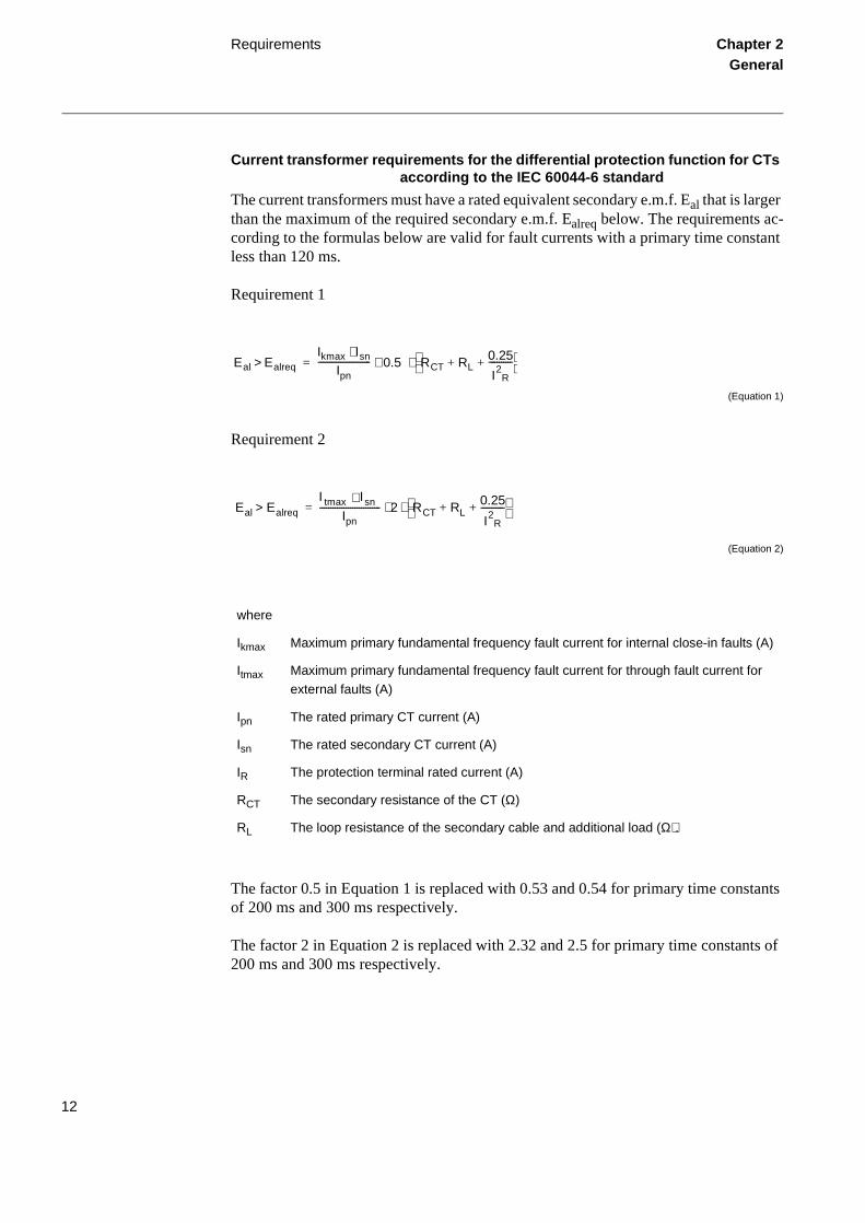
Current transformer requirements for the differential protection function for CTs according to the IEC 60044-6 standard
The current transformers must have a rated equivalent secondary e.m.f. Eal that is larger than the maximum of the required secondary e.m.f. Ealreq below. The requirements ac-cording to the formulas below are valid for fault currents with a primary time constant less than 120 ms.
Requirement 1
(Equation 1)
Requirement 2
(Equation 2)
The factor 0.5 in Equation 1 is replaced with 0.53 and 0.54 for primary time constants of 200 ms and 300 ms respectively.
The factor 2 in Equation 2 is replaced with 2.32 and 2.5 for primary time constants of 200 ms and 300 ms respectively.
where
Ikmax Maximum primary fundamental frequency fault current for internal close-in faults (A)
Itmax Maximum primary fundamental frequency fault current for through fault current for external faults (A)
Ipn The rated primary CT current (A)
Isn The rated secondary CT current (A)
IR The protection terminal rated current (A)
RCT The secondary resistance of the CT (Ω)
RL The loop resistance of the secondary cable and additional load (Ω).
Eal Ealreq>Ikmax Isn⋅
Ipn------------------------ 0.5 RCT RL
0.25
I2R
-----------+ + ⋅ ⋅=
Eal Ealreq>I tmax Isn⋅
Ipn---------------------------- 2 RCT RL
0.25
I2R
-----------+ + ⋅ ⋅=
12
Requirements Chapter 2General
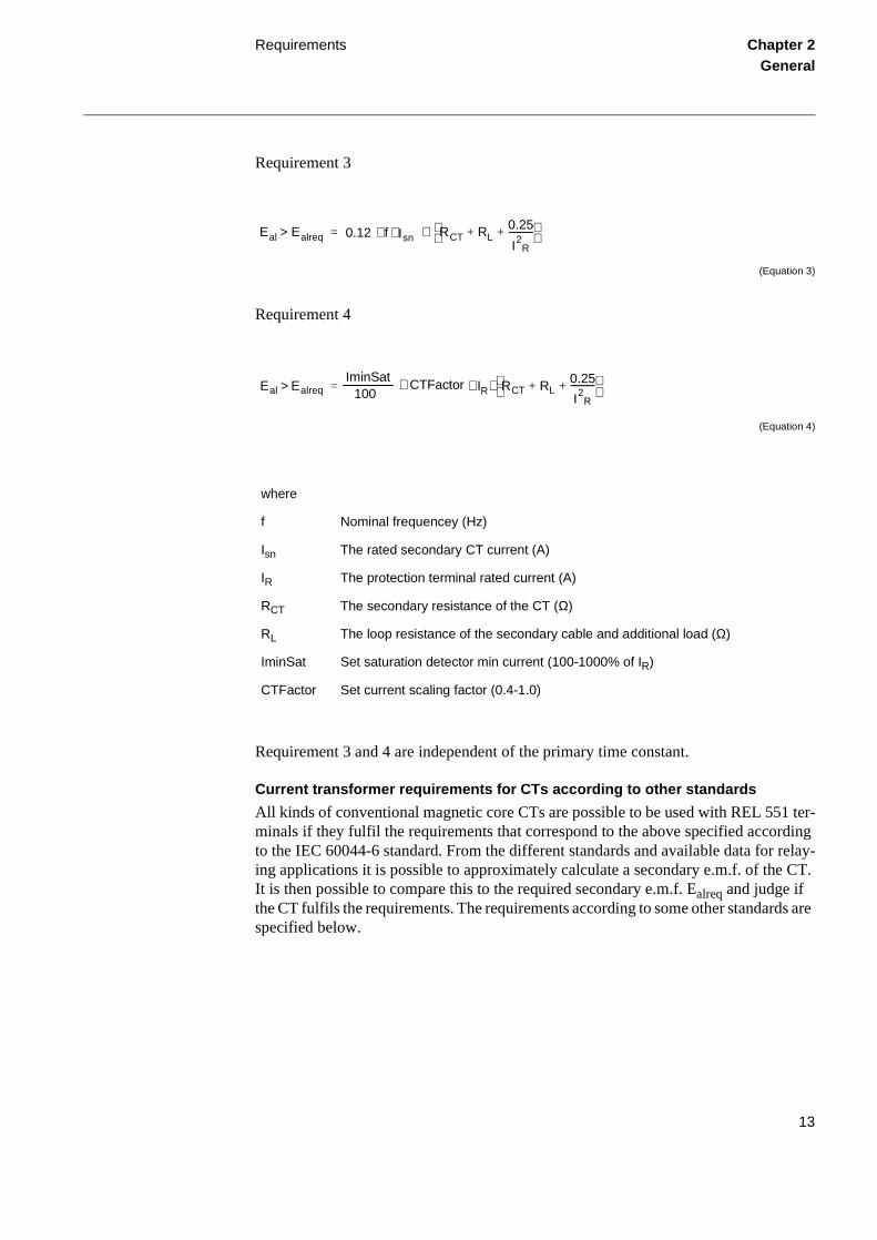
Requirement 3
(Equation 3)
Requirement 4
(Equation 4)
Requirement 3 and 4 are independent of the primary time constant.
Current transformer requirements for CTs according to other standards
All kinds of conventional magnetic core CTs are possible to be used with REL 551 ter-minals if they fulfil the requirements that correspond to the above specified according to the IEC 60044-6 standard. From the different standards and available data for relay-ing applications it is possible to approximately calculate a secondary e.m.f. of the CT. It is then possible to compare this to the required secondary e.m.f. Ealreq and judge if the CT fulfils the requirements. The requirements according to some other standards are specified below.
where
f Nominal frequencey (Hz)
Isn The rated secondary CT current (A)
IR The protection terminal rated current (A)
RCT The secondary resistance of the CT (Ω)
RL The loop resistance of the secondary cable and additional load (Ω)
IminSat Set saturation detector min current (100-1000% of IR)
CTFactor Set current scaling factor (0.4-1.0)
Eal Ealreq> I RCT RL0.25
I2R
-----------+ + ⋅ ⋅= 0.12 ⋅ f sn
Eal Ealreq>IminSat
100I RCT RL
0.25
I2R
-----------+ + ⋅ ⋅= CTFactor⋅ R
13
Requirements Chapter 2General
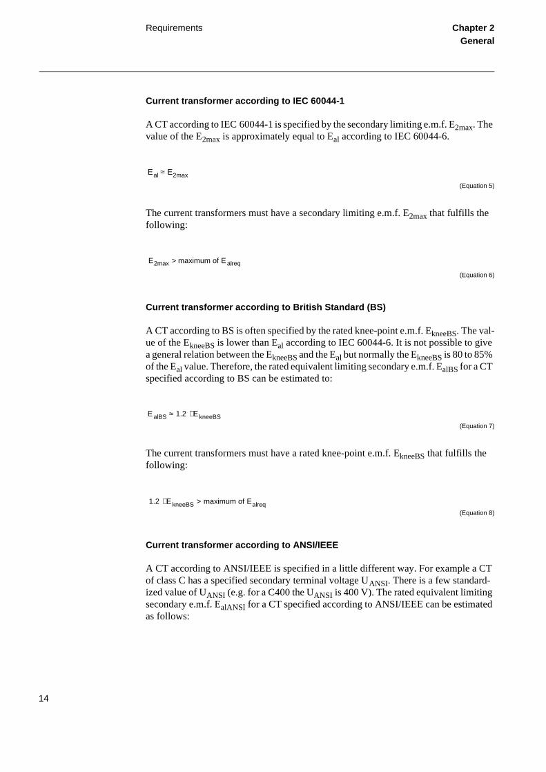
Current transformer according to IEC 60044-1
A CT according to IEC 60044-1 is specified by the secondary limiting e.m.f. E2max. The value of the E2max is approximately equal to Eal according to IEC 60044-6.
(Equation 5)
The current transformers must have a secondary limiting e.m.f. E2max that fulfills the following:
(Equation 6)
Current transformer according to British Standard (BS)
A CT according to BS is often specified by the rated knee-point e.m.f. EkneeBS. The val-ue of the EkneeBS is lower than Eal according to IEC 60044-6. It is not possible to give a general relation between the EkneeBS and the Eal but normally the EkneeBS is 80 to 85% of the Eal value. Therefore, the rated equivalent limiting secondary e.m.f. EalBS for a CT specified according to BS can be estimated to:
(Equation 7)
The current transformers must have a rated knee-point e.m.f. EkneeBS that fulfills the following:
(Equation 8)
Current transformer according to ANSI/IEEE
A CT according to ANSI/IEEE is specified in a little different way. For example a CT of class C has a specified secondary terminal voltage UANSI. There is a few standard-ized value of UANSI (e.g. for a C400 the UANSI is 400 V). The rated equivalent limiting secondary e.m.f. EalANSI for a CT specified according to ANSI/IEEE can be estimated as follows:
Eal E2max≈
E2max maximum of Ealreq>
E alBS 1.2 E kneeBS⋅≈
1.2 EkneeBS maximum of Ealreq>⋅
14
Requirements Chapter 2General
(Equation 9)
The CT requirements are fulfilled if:
(Equation 10)
Often an ANSI/IEEE CT also has a specified knee-point voltage UkneeANSI. This is graphically defined from the excitation curve. The knee-point according to ANSI/IEEE has normally a lower value than the knee-point according to BS. The rated equivalent limiting secondary e.m.f. EalANSI for a CT specified according to ANSI/IEEE can be estimated to:
(Equation 11)
The current transformers must have a knee-point voltage UkneeANSI that fulfills the fol-lowing:
ZbANSI The impedance (i.e. complex quantity) of the standard ANSI burden for the specific C
class (Ω)
UANSI The secondary terminal voltage for the specific C class (V)
EalANSI 20 Isn R CT U ANSI+⋅ ⋅ 20 Isn R CT 20 I sn ZbANSI⋅ ⋅+⋅ ⋅= =
EalANSI maximum of Ealreq>
EalANSI 1.3 UkneeANSI⋅≈
1.3 UkneeANSI maximum of Ealreq>⋅
15
Terminal identification Chapter 2General
ed ut the
trans- the calcu-base al for
5 Terminal identification
5.1 Application
Serial number, software version and the identification names and numbers for the sta-tion, the object and the terminal (unit) itself can be stored in the REx 5xx terminal. Also the serial numbers of included modules are stored in the terminal. This information can be read on the local HMI or when communicating with the terminal through a PC or with SMS/SCS.
The base currents, voltages and rated frequency must be set since the values affect many functions. The input transformers ratio must be set as well. The ratio for the current and the voltage transformer automatically affects the measuring functions in the terminal.
The internal clock is used for time tagging of:
• Internal events
• Disturbance reports
• Events in a disturbance report
• Events transmitted to the SCS substation control system
This implies that the internal clock is very important. The clock can be synchroniz(see Time synchronization) to achieve higher accuracy of the time tagging. Withosynchronization, the internal clock is useful for comparisons among events withinREx 5xx terminal.
5.2 Calculations
Uxr and Ixr (x = 1-5) are the rated voltage and current values for the analog input formers within the REx 5xx terminal. UxScale and IxScale are the actual ratio formain protection transformer at the protected object. These values will be used to late the present voltage and current in the protected object. Uxb and Ixb defines voltage and current values, used to define the per-unit system used in the termincalculation of setting values.
The current transformer secondary current (IsSEC) is:
(Equation 12)
IsSEC
ISEC
IPRIM------------- Is⋅=
16

Terminal identification Chapter 2General
The relay setting value IP>> is given in percentage of the secondary base current value, Ixb, associated to the current transformer input Ix:
(Equation 13)
The value of Ixb can be calculated as:
(Equation 14)
where:
ISEC = secondary rated current of the main CT
IPRIM = primary rated current of the main CT
Is = primary setting value of the current
IP>>IsSEC
Ixb-------------- 100⋅=
Ixb Rated primary currentCT ratio
----------------------------------------------------------=
17

Terminal identification Chapter 2General
18

About this chapter Chapter 3Common functions
Chapter 3 Common functions
About this chapter
This chapter presents the common functions in the terminal.
19
Time synchronisation (TIME) Chapter 3Common functions
1 Time synchronisation (TIME)
1.1 Application
Use time synchronisation to achieve a common time base for the terminals in a protec-tion and control system. This makes comparision of events and disturbance data be-tween all terminals in the system possible.
Time-tagging of internal events and disturbances is an excellent help when evaluating faults. Without time synchronisation, only the events within the terminal can be com-pared to one another. With time synchronisation, events and disturbances within the en-tire station, and even between line ends, can be compared during an evaluation.
1.2 Functionality
Two main alternatives of external time synchronisation is available. Either the synchro-nisation message is applied via any of the communication ports of the terminal as a tele-gram message including date and time, or as a minute pulse, connected to a binary input. The minute pulse is used to fine tune already existing time in the terminals.
The REx 5xx terminal has its own internal clock with date, hour, minute, second and millisecond. It has a resolution of 1 ms.
The clock has a built-in calendar for 30 years that handles leap years. Any change be-tween summer and winter time must be handled manually or through external time syn-chronisation. The clock is powered by a capacitor, to bridge interruptions in power supply without malfunction.
The internal clock is used for time-tagging disturbances, events in Substation monitor-ing system (SMS) and Substation control system (SCS), and internal events.
1.3 Calculations
The internal time can be set on the local human-machine interface (HMI) at:
Settings
Time
The time is set with year, month, day and time.
The source of the time synchronisation is set on the local HMI at:
20

Time synchronisation (TIME) Chapter 3Common functions
N-
HMI ock set
Configuration
Time
When the setting is performed on the local HMI, the parameter is called TimeSync-Source. The time synchronisation source can also be set from the CAP 531 tool. The setting parameter is then called SYNCSCR. The setting alternatives are:
• None (no synchronisation)
• LON
• SPA
• IEC
• Minute pulse positive flank
• Minute pulse negative flank
The function input to be used for minute-pulse synchronisation is called TIME-MISYNC.
The internal time can be set manually down to the minute level, either via the local or via any of the communication ports. The time synchronisation fine tunes the cl(seconds and milliseconds). If no clock synchronisation is active, the time can bedown to milliseconds.
21
Setting group selector (GRP) Chapter 3Common functions
2 Setting group selector (GRP)
2.1 Application
Different conditions in networks of different voltage levels require high adaptability of the used protection and control units to best provide for dependability, security and se-lectivity requirements. Protection units operate with higher degree of availability, espe-cially, if the setting values of their parameters are continuously optimised regarding the conditions in power system.
The operational departments can plan different operating conditions for the primary equipment. The protection engineer can prepare in advance for the necessary optimised and pre-tested settings for different protection functions. Four different groups of set-ting parameters are available in the REx 5xx terminals. Any of them can be activated automatically through up to four different programmable binary inputs by means of ex-ternal control signals.
2.2 Functionality
Select a setting group by using the local HMI, from a front connected personal comput-er, remotely from the station control or station monitoring system or by activating the corresponding input to the GRP function block.
Each input of the function block is configurable to any of the binary inputs in the ter-minal. Configuration must be performed under the menu:
Configuration
Functions
Active Group
FuncInputs
Use external control signals to activate a suitable setting group when adaptive function-ality is necessary. Input signals that should activate setting groups must be either per-manent or a pulse longer than 200 ms.
More than one input may be activated simultaneously. In such cases the lower order set-ting group has priority. This means that if for example both group four and group two are set to activate, group two will be the one activated.
22
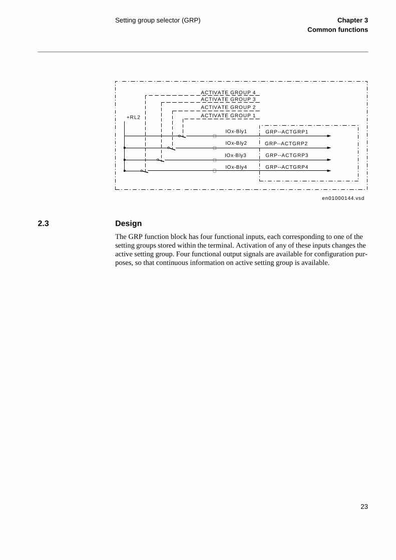
Setting group selector (GRP) Chapter 3Common functions
2.3 Design
The GRP function block has four functional inputs, each corresponding to one of the setting groups stored within the terminal. Activation of any of these inputs changes the active setting group. Four functional output signals are available for configuration pur-poses, so that continuous information on active setting group is available.
GRP--ACTGRP1
GRP--ACTGRP2
GRP--ACTGRP3
GRP--ACTGRP4
IOx-Bly1
IOx-Bly2
IOx-Bly3
IOx-Bly4
+RL2
∅
∅
∅
∅
en01000144.vsd
ACTIVATE GROUP 4ACTIVATE GROUP 3
ACTIVATE GROUP 2
ACTIVATE GROUP 1
23
Setting lockout (HMI) Chapter 3Common functions
3 Setting lockout (HMI)
3.1 Application
Unpermitted or uncoordinated changes by unauthorized personnel may cause severe damage to primary and secondary power circuits. Use the setting lockout function to prevent unauthorized setting changes and to control when setting changes are allowed.
By adding a key switch connected to a binary input a simple setting change control cir-cuit can be built simply allowing only authorized keyholders to make setting changes. Security can be increased by adding SA/SMS overrides that prevents changes even by keyholders.
3.2 Functionality
Activating the setting restriction prevents unauthorized personell to purposely or by mistake change terminal settings.
The HMI--BLOCKSET functional input is configurable only to one of the available bi-nary inputs of a REx 5xx terminal. For this reason, the terminal is delivered with the default configuration, where the HMI--BLOCKSET signal is connected to NONE-NOSIGNAL.
The function permits remote changes of settings and reconfiguration through the serial communication ports. The setting restrictions can be activated only from the local HMI.
All other functions of the local human-machine communication remain intact. This means that an operator can read all disturbance reports and other information and set-ting values for different protection parameters and the configuration of different logic circuits.
24

Setting lockout (HMI) Chapter 3Common functions
Figure 1: Connection and logic diagram for the BLOCKSET function
SettingRestrict=BlockRESTRICTSETTINGS
HMI--BLOCKSET
&SWITCH
WITH KEY
+
Rex 5xx
en01000152.vsd
25
I/O system configurator (IOP) Chapter 3Common functions
-
size
put/. The
r put
e mA
the
tion. g.
4 I/O system configurator (IOP)
4.1 Application
The I/O system configurator must be used in order to recognize added modules and to create internal adress mappings between modules and protections and other functions.
4.2 Functionality
The I/O system configurator is used to add, remove or move I/O modules in the REx 5xx terminals. To configure means to connect the function blocks that represent each I/O module (BIM, BOM, IOM, IOPSM, DCM and MIM) to a function block for the I/O positions (IOP1) that represent the physical slot in the rack.
Available I/O modules are:
• BIM, Binary Input Module with 16 binary input channels.
• BOM, Binary Output Module with 24 binary output channels.
• IOM, Input/Output Module with 8 binary input and 12 binary output channels.
• MIM, mA Input Module with six analog input channels.
• IOPSM, Input Output Power Supply Module with four inputs and four outputs.
• DCM, Data Communication Module. The only software configuration for this module is the I/O Position input.
An REx 5xx terminal houses different numbers of modules depending of the casingand which kind of modules chosen.
• The 1/1 of 19-inch size casing houses a maximum of 13 modules. But when InOutput- or Output modules are included, the maximum of these modules are sixmaximum number of mA Input modules are also limited to six.
• The 3/4-size casing houses a maximum of eight modules. The limitation is foumodules for Input/Output- or Output modules. The maximum number of mA Inmodules are three.
• The 1/2-size casing houses a maximum of three binary modules or one analoguInput module.
It is possible to fit modules of different types in any combination in a terminal, buttotal maximum numbers of modules must be considered.
Each I/O-module can be placed in any CAN-I/O slot in the casing with one excepThe DCM-module has a fixed slot position which depends on the size of the casin
26
I/O system configurator (IOP) Chapter 3Common functions
To add, remove or move modules in the terminal, the reconfiguration of the terminal must be done from the graphical configuration tool CAP 531.
Users refer to the CAN-I/O slots by the physical slot numbers of the CAN-I/O slots, which also appear in the terminal drawings.
If the user-entered configuration does not match the actual configuration in the termi-nal, an error output is activated on the function block, which can be treated as an event or alarm.
The BIM, BOM, IOM, IOPSM and DCM share the same communication addresses for parameters and configuration. So they must share I/O module 1-13 (IOxx), which are the same function block. A user-configurable function selector per I/O module function block determines which type of module it is.
All names for inputs and outputs are inputs on the function blocks and must be set from the graphical tool CAP 531.
I/O position
The IOP1 (I/O position) function block is the same for the different casings, indepen-dent of the number of slots available. Anyway, it looks different depending of actual configuration. All necessary configuration is done in the CAP 531 configuration tool.
The Sxx outputs are connected to the POSITION inputs of the I/O Modules and MIMs.
27
I/O system configurator (IOP) Chapter 3Common functions
ule
t of
Figure 2: Function block of the I/O position block (IOP1-).
Configuration
The I/O-configuration can only be performed from CAP 531, the graphical configura-tion tool.
To configure from the graphical tool:
• First, set the function selector for the logical I/O module to the type of I/O modthat is used, BIM, BOM, IOM, IOPSM or DCM.
• Secondly, connect the POSITION input of the logical I/O module to a slot outputhe IOP function block.
xx00000238.vsd
IOP1-I/OPOSITION
S11S12S13S14S15S16S17S18S19S20S21S22S23S24S25S26S27S28S29S30S31S32S33S34S35S36
28
I/O system configurator (IOP) Chapter 3Common functions
Figure 3: Example of an I/O-configuration in the graphical tool CAP 531 for a REx 5xx with two BIMs.
I/O-MODULEIO01-
POSITION ERRORBI1
. .
.BI16
I/O-MODULEIO02-
POSITION ERRORBI1
. .
.BI16
IOP1-I/OPOSITION
S11S13S15S17S19
en01000142.vsd
29
Logic function blocks Chapter 3Common functions
5 Logic function blocks
5.1 Application
5.1.1 Application
Different protection, control, and monitoring functions within the REx 5xx terminals are quite independent as far as their configuration in the terminal is concerned. The user cannot enter and change the basic algorithms for different functions, because they are located in the digital signal processors and extensively type tested. The user can config-ure different functions in the terminals to suit special requirements for different appli-cations.
For this purpose, additional logic circuits are needed to configure the terminals to meet user needs and also to build in some special logic circuits, which use different logic gates and timers.
5.2 Functionality
Inverter (INV)
The INV function block is used to invert the input boolean variable. The function block (figure 4) has one input designated IVnn-INPUT where nn presents the serial number of the block. Each INV circuit has one output IVnn-OUT.
Figure 4: Function block diagram of the inverter (INV) function
Table 1: Truth table for the INV function block
INPUT OUT
1 0
0 1
1INPUT OUT
IVnn
99000021.vsd
30

Logic function blocks Chapter 3Common functions
Controllable gate (GT)
The GT function block is used for controlling if a signal should be able to pass or not depending on a setting. The function block (figure 5) has one input, designated GTnn-INPUT, where nn presents the serial number of the block. Each GT circuit has one out-put, GTnn-OUT. Each gate further has a Operation On/Off which controls if the INPUT is passed to the OUT or not.
Figure 5: Function block diagram of the controllable gate (GT) function
The output signal from the GT function block is set to 1 if the input signal is 1 and Op-eration = On elsewhere it is set to 0. See truth table below.
Table 2: Truth table for the GT function block
OR
OR function blocks are used to form general combinatory expressions with boolean variables. The function block (figure 6) has six inputs, designated Onnn-INPUTm, where nnn presents the serial number of the block, and m presents the serial number of the inputs in the block. Each OR circuit has two outputs, Onnn-OUT and Onnn-NOUT (inverted).
INPUT Operation OUT
0 Off 0
1 Off 0
0 On 0
1 On 1
&Operation = On
INPUTOUT
GTnn
xx00000530.vsd
31

Logic function blocks Chapter 3Common functions
Figure 6: Function block diagram of the OR function
The output signal (OUT) is set to 1 if any of the inputs (INPUT1-6) is 1. See truth table below.
Table 3: Truth table for the OR function block
AND
AND function blocks are used to form general combinatory expressions with boolean variables. The function block (figure 7) has four inputs (one of them inverted), desig-nated Annn-INPUTm (Annn-INPUT4N is inverted), where nnn presents the serial number of the block, and m presents the serial number of the inputs in the block. Each AND circuit has two outputs, Annn-OUT and Annn-NOUT (inverted).
≥1
INPUT6
INPUT1
INPUT2
INPUT3
INPUT4
INPUT5
OUT
1NOUT
Onnn
xx00000514.vsd
INPUT1 INPUT2 INPUT3 INPUT4 INPUT5 INPUT6 OUT NOUT
0 0 0 0 0 0 0 1
0 0 0 0 0 1 1 0
0 0 0 0 1 0 1 0
... ... ... ... ... ... 1 0
1 1 1 1 1 0 1 0
1 1 1 1 1 1 1 0
32
Logic function blocks Chapter 3Common functions
Figure 7: Function block diagram of the AND function
The output signal (OUT) is set to 1 if the inputs INPUT1-3 are 1 and INPUT4N is 0. See truth table below.
Table 4: Truth table for the OR function block
INPUT1 INPUT2 INPUT3 INPUT4N OUT NOUT
0 0 0 1 0 1
0 0 1 1 0 1
0 1 0 1 0 1
0 1 1 1 0 1
1 0 0 1 0 1
1 0 1 1 0 1
1 1 0 1 0 1
1 1 1 1 0 1
0 0 0 0 0 1
0 0 1 0 0 1
0 1 0 0 0 1
0 1 1 0 0 1
1 0 0 0 0 1
1 0 1 0 0 1
1 1 0 0 0 1
1 1 1 0 1 0
xx00000515.vsd
&INPUT1
INPUT2
INPUT3
INPUT4
OUT
1NOUT
Annn
33

Logic function blocks Chapter 3Common functions
Timer
The function block TM timer has outputs for delayed input signal at drop-out and at pick-up. The timer (figure 8) has a settable time delay TMnn-T between 0.00 and 60.00 s in steps of 0.01 s. The input signal for each time delay block has the designation TMnn-INPUT, where nn presents the serial number of the logic block. The output sig-nals of each time delay block are TMnn-ON and TMnn-OFF. The first one belongs to the timer delayed on pick-up and the second one to the timer delayed on drop-out. Both timers within one block always have the same setting.
Figure 8: Function block diagram of the Timer function
The function block TL timer (figure 9) with extended maximum time delay at pick-up and at drop-out, is identical with the TM timer. The difference is the longer time delay TLnn-T, settable between 0.0 and 90000.0 s in steps of 0.1 s.
xx00000523.vsd
OFFINPUT
ON
TTime delay 0.00-60.00s
TMnn
t
t
34
Logic function blocks Chapter 3Common functions
Figure 9: Function block diagram of the TimerLong function
The input variable to INPUT is obtained delayed a settable time T at output OFF when the input variable changes from 1 to 0 in accordance with the time pulse diagram, figure 10. The output OFF signal is set to 1 immediately when the input variable changes from 0 to 1.
Figure 10: Example of time diagram for a timer delayed on drop-out with preset time T = 3 s
xx00000526.vsd
OFFINPUT
ON
TTime delay 0.0-90000.0s
TLnn
t
t
xx00000528.vsd
INPUT
OFF
T=3s
1
0
1
0
0 11 2 3 4 5 6 7 8 9 10
35
Logic function blocks Chapter 3Common functions
The input variable to INPUT is obtained delayed a settable time T at output ON when the input variable changes from 0 to 1 in accordance with the time pulse diagram, figure 11. The output ON signal returns immediately when the input variable changes from 1 to 0.
Figure 11: Example of time diagram for a timer delayed on pick-up with preset time T = 3 s
If more timers than available in the terminal are needed, it is possible to use pulse timers with AND or OR logics. Figure 12 shows an application example of how to realize a timer delayed on pick-up. Figure 13 shows the realization of a timer delayed on drop-out. Note that the resolution of the set time must be 0.2 s, if the connected logic has a cycle time of 200 ms.
Figure 12: Realization example of a timer delayed on pick-up
INPUT
ON
T=3s
1
0
1
0
0 11 2 3 4 5 6 7 8 9 10
xx00000529.vsd
AND
INPUT1INPUT2INPUT3INPUT4N
OUTNOUT
Pulse
INPUTT
OUTNOUT
FIXED-ON
0.00-60.00s
xx00000533.vsd
36
Logic function blocks Chapter 3Common functions
Figure 13: Realization example of a timer delayed on drop-out
Timer settable through HMI/SMS/PST
The function block TS timer has outputs for delayed input signal at drop-out and at pick-up. The timer (figure 14) has a settable time delay TSnn-T between 0.00 and 60.00 s in steps of 0.01 s. It also has an Operation setting On, Off which controls the operation of the timer.The input signal for each time delay block has the designation TSnn-IN-PUT, where nn presents the serial number of the logic block. The output signals of each time delay block are TSnn-ON and TSnn-OFF. The first one belongs to the timer de-layed on pick-up and the second one to the timer delayed on drop-out. Both timers with-in one block always have the same setting.
Figure 14: Function block diagram of the Settable timer function
INV
INPUT OUT
ORINPUT1INPUT2
OUTNOUT
INPUT3INPUT4INPUT5INPUT6
FIXED-OFF
Pulse
INPUT
T
OUT
0.00-60.00s
xx00000534.vsd
&Operation = On
INPUT
TSnn
t OFF
t ON
Time delay T=0.00-60.00s
xx00000531.vsd
37
Logic function blocks Chapter 3Common functions
For details about the function see the description of TM Timer.
Pulse
The pulse function can be used, for example, for pulse extensions or limiting of opera-tion of outputs. The pulse timer TP (figure 15) has a settable length of a pulse between 0.00 s and 60.00 s in steps of 0.01 s. The input signal for each pulse timer has the des-ignation TPnn-INPUT, where nn presents the serial number of the logic block. Each pulse timer has one output, designated by TPnn-OUT. The pulse timer is not retrigga-ble, that is, it can be restarted first after that the time T has elapsed.
Figure 15: Function block diagram of the Pulse function
The function block TQ pulse timer (figure 16) with extended maximum pulse length, is identical with the TP pulse timer. The difference is the longer pulse length TQnn-T, set-table between 0.0 and 90000.0 s in steps of 0.1 s.
Figure 16: Function block diagram of the PulseLong function, TQ
OUTINPUT
T Time delay 0.00-60.00s
TPnn
xx00000524.vsd
OUTINPUT
T Time delay 0.0-90000.0s
TQnn
xx00000525.vsd
38
Logic function blocks Chapter 3Common functions
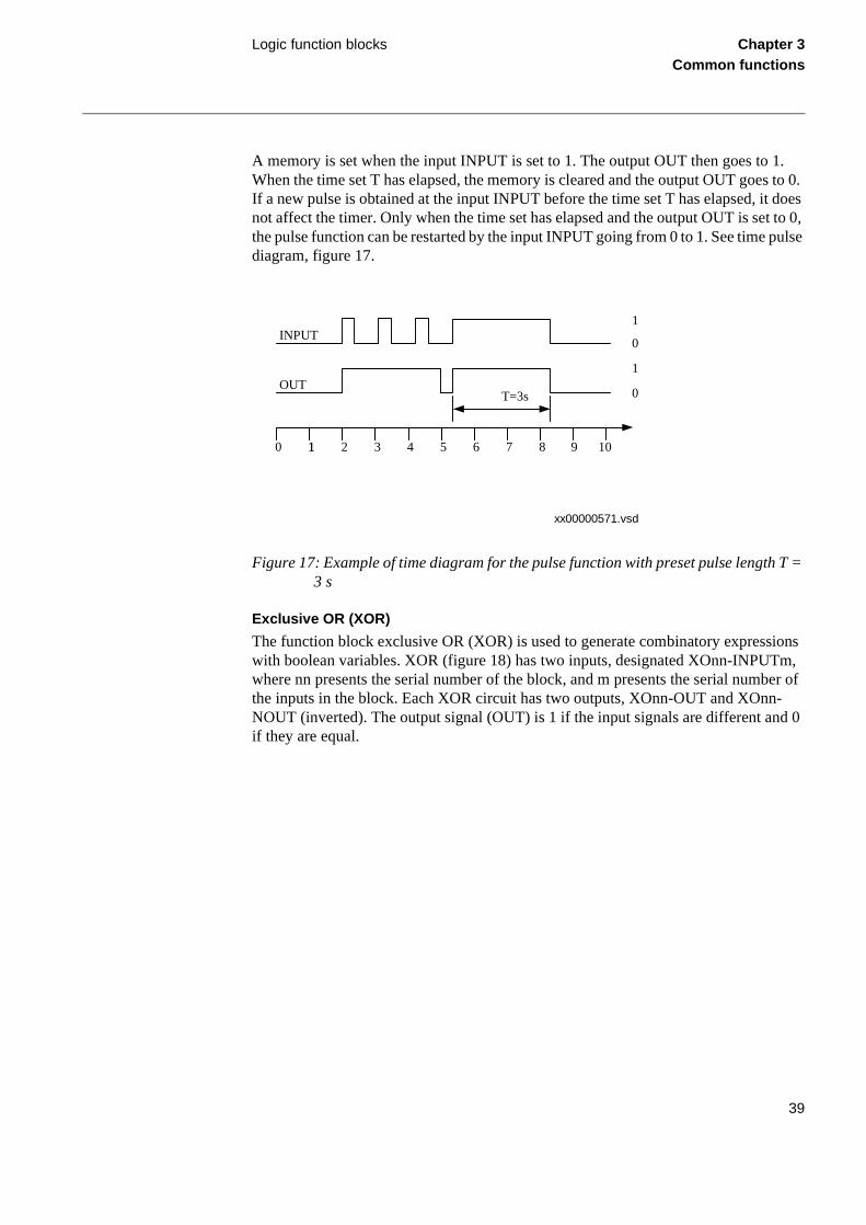
A memory is set when the input INPUT is set to 1. The output OUT then goes to 1. When the time set T has elapsed, the memory is cleared and the output OUT goes to 0. If a new pulse is obtained at the input INPUT before the time set T has elapsed, it does not affect the timer. Only when the time set has elapsed and the output OUT is set to 0, the pulse function can be restarted by the input INPUT going from 0 to 1. See time pulse diagram, figure 17.
Figure 17: Example of time diagram for the pulse function with preset pulse length T = 3 s
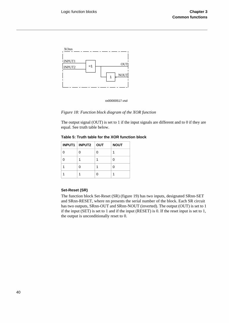
Exclusive OR (XOR)
The function block exclusive OR (XOR) is used to generate combinatory expressions with boolean variables. XOR (figure 18) has two inputs, designated XOnn-INPUTm, where nn presents the serial number of the block, and m presents the serial number of the inputs in the block. Each XOR circuit has two outputs, XOnn-OUT and XOnn-NOUT (inverted). The output signal (OUT) is 1 if the input signals are different and 0 if they are equal.
T=3s
1
0
1
0
0 11 2 3 4 5 6 7 8 9 10
INPUT
OUT
xx00000571.vsd
39
Logic function blocks Chapter 3Common functions
Figure 18: Function block diagram of the XOR function
The output signal (OUT) is set to 1 if the input signals are different and to 0 if they are equal. See truth table below.
Table 5: Truth table for the XOR function block
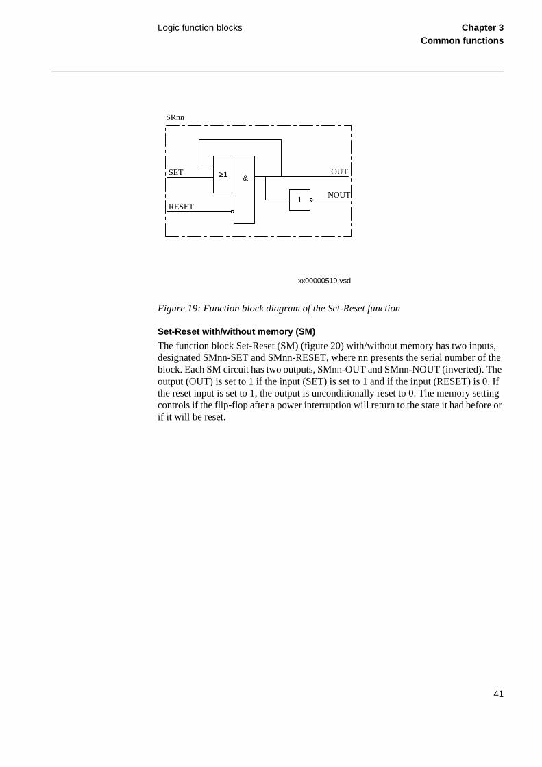
Set-Reset (SR)
The function block Set-Reset (SR) (figure 19) has two inputs, designated SRnn-SET and SRnn-RESET, where nn presents the serial number of the block. Each SR circuit has two outputs, SRnn-OUT and SRnn-NOUT (inverted). The output (OUT) is set to 1 if the input (SET) is set to 1 and if the input (RESET) is 0. If the reset input is set to 1, the output is unconditionally reset to 0.
INPUT1 INPUT2 OUT NOUT
0 0 0 1
0 1 1 0
1 0 1 0
1 1 0 1
=1OUT
1NOUT
INPUT1
INPUT2
XOnn
xx00000517.vsd
40
Logic function blocks Chapter 3Common functions
Figure 19: Function block diagram of the Set-Reset function
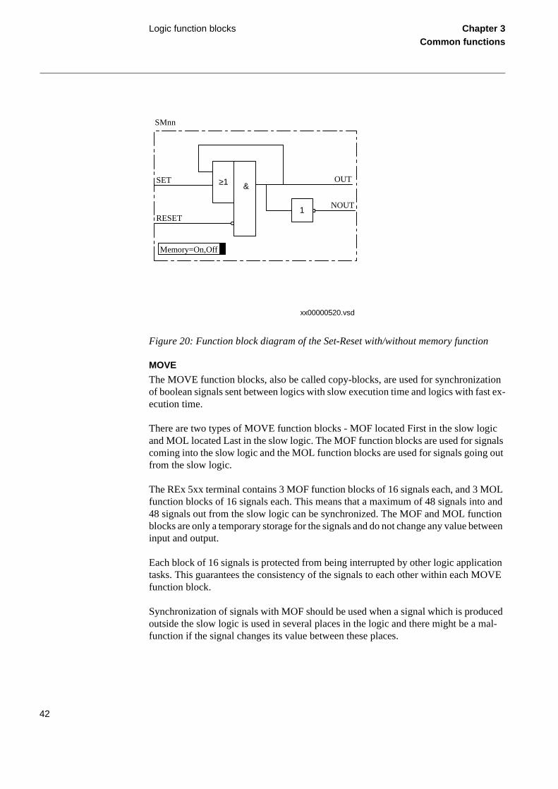
Set-Reset with/without memory (SM)
The function block Set-Reset (SM) (figure 20) with/without memory has two inputs, designated SMnn-SET and SMnn-RESET, where nn presents the serial number of the block. Each SM circuit has two outputs, SMnn-OUT and SMnn-NOUT (inverted). The output (OUT) is set to 1 if the input (SET) is set to 1 and if the input (RESET) is 0. If the reset input is set to 1, the output is unconditionally reset to 0. The memory setting controls if the flip-flop after a power interruption will return to the state it had before or if it will be reset.
OUTSET
RESET
&≥1
1NOUT
SRnn
xx00000519.vsd
41
Logic function blocks Chapter 3Common functions
Figure 20: Function block diagram of the Set-Reset with/without memory function
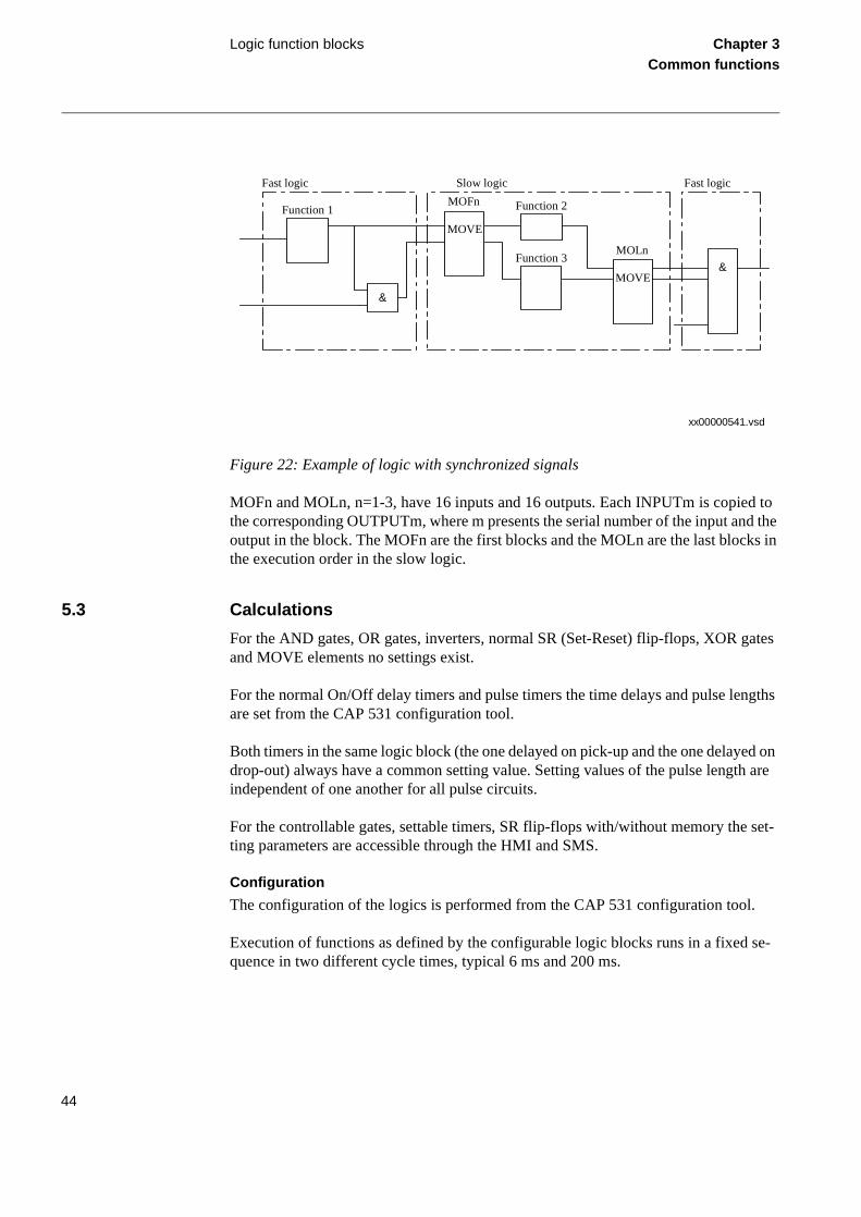
MOVE
The MOVE function blocks, also be called copy-blocks, are used for synchronization of boolean signals sent between logics with slow execution time and logics with fast ex-ecution time.
There are two types of MOVE function blocks - MOF located First in the slow logic and MOL located Last in the slow logic. The MOF function blocks are used for signals coming into the slow logic and the MOL function blocks are used for signals going out from the slow logic.
The REx 5xx terminal contains 3 MOF function blocks of 16 signals each, and 3 MOL function blocks of 16 signals each. This means that a maximum of 48 signals into and 48 signals out from the slow logic can be synchronized. The MOF and MOL function blocks are only a temporary storage for the signals and do not change any value between input and output.
Each block of 16 signals is protected from being interrupted by other logic application tasks. This guarantees the consistency of the signals to each other within each MOVE function block.
Synchronization of signals with MOF should be used when a signal which is produced outside the slow logic is used in several places in the logic and there might be a mal-function if the signal changes its value between these places.
xx00000520.vsd
OUTSET
RESET
&≥1
1NOUT
SMnn
Memory=On,Off
42
Logic function blocks Chapter 3Common functions
Synchronization with MOL should be used if a signal produced in the slow logic is used in several places outside this logic, or if several signals produced in the slow logic are used together outside this logic, and there is a similar need for synchronization.
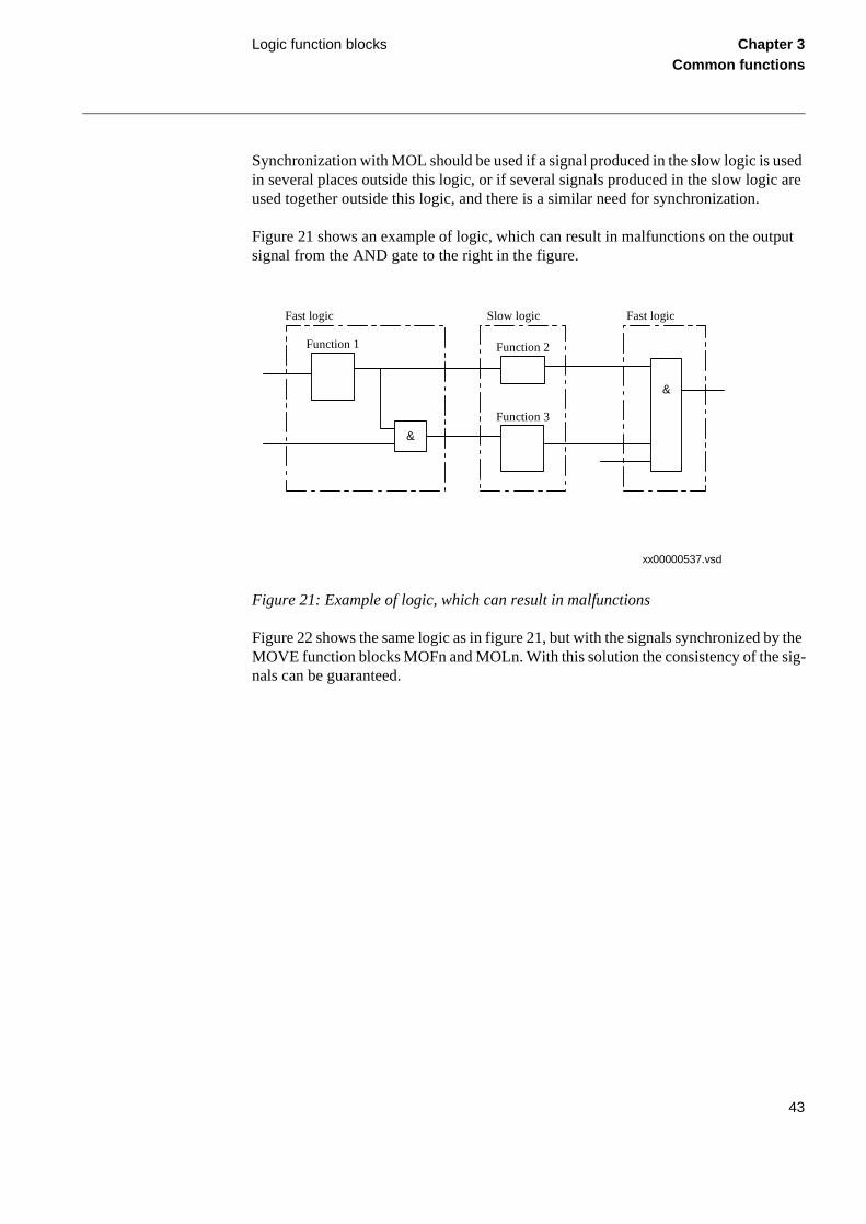
Figure 21 shows an example of logic, which can result in malfunctions on the output signal from the AND gate to the right in the figure.
Figure 21: Example of logic, which can result in malfunctions
Figure 22 shows the same logic as in figure 21, but with the signals synchronized by the MOVE function blocks MOFn and MOLn. With this solution the consistency of the sig-nals can be guaranteed.
Function 1 Function 2
&
Function 3
&
Fast logic Slow logic Fast logic
xx00000537.vsd
43
Logic function blocks Chapter 3Common functions
Figure 22: Example of logic with synchronized signals
MOFn and MOLn, n=1-3, have 16 inputs and 16 outputs. Each INPUTm is copied to the corresponding OUTPUTm, where m presents the serial number of the input and the output in the block. The MOFn are the first blocks and the MOLn are the last blocks in the execution order in the slow logic.
5.3 Calculations
For the AND gates, OR gates, inverters, normal SR (Set-Reset) flip-flops, XOR gates and MOVE elements no settings exist.
For the normal On/Off delay timers and pulse timers the time delays and pulse lengths are set from the CAP 531 configuration tool.
Both timers in the same logic block (the one delayed on pick-up and the one delayed on drop-out) always have a common setting value. Setting values of the pulse length are independent of one another for all pulse circuits.
For the controllable gates, settable timers, SR flip-flops with/without memory the set-ting parameters are accessible through the HMI and SMS.
Configuration
The configuration of the logics is performed from the CAP 531 configuration tool.
Execution of functions as defined by the configurable logic blocks runs in a fixed se-quence in two different cycle times, typical 6 ms and 200 ms.
Function 1 Function 2
Function 3
&
Fast logic Slow logic
MOFn
MOVE
MOLn
MOVE&
Fast logic
xx00000541.vsd
44

Logic function blocks Chapter 3Common functions
For each cycle time, the function block is given an execution serial number. This is shown when using the CAP 531 configuration tool with the designation of the function block and the cycle time, for example, TMnn-(1044, 6). TMnn is the designation of the function block, 1044 is the execution serial number and 6 is the cycle time.
Execution of different function blocks within the same cycle time should follow the same order as their execution serial numbers to get an optimal solution. Always remem-ber this when connecting in series two or more logical function blocks. When connect-ing function blocks with different cycle times, the MOVE function blocks can be used. These function blocks synchronize boolean signals sent between logics with slow exe-cution time and logics with fast execution time. The MOVE functions are available as additional configurable logic circuits.
Note!
Be always careful when connecting function blocks with a fast cycle time to functionblocks with a slow cycle time.
So design the logic circuits carefully and check always the execution sequence for dif-ferent functions. In other cases, additional time delays must be introduced into the logicschemes to prevent errors, for example, race between functions.
45

Self supervision (INT) Chapter 3Common functions
The n it is ot be
g
nect-
6 Self supervision (INT)
6.1 Application
The REx 5xx protection and control terminals have a complex design with many includ-ed functions. The included self-supervision function and the INTernal signals function block provide good supervision of the terminal. The different safety measures and fault signals makes it easier to analyze and locate a fault.
Both hardware and software supervision is included and it is also possible to indicate possible faults through a hardware contact and/or through the software communication.
Internal events are generated by the built-in supervisory functions. The supervisory functions supervise the status of the various modules in the terminal and, in case of fail-ure, a corresponding event is generated. Similarly, when the failure is corrected, a cor-responding event is generated.
Apart from the built-in supervision of the various modules, events are also generated when the status changes for the:
• built-in real time clock (in operation/out of order).
• external time synchronization (in operation/out of order).
Events are also generated:
• whenever any setting in the terminal is changed.
• when the content of the Disturbance report is erased.
The internal events are time tagged with a resolution of 1 ms and stored in a list.list can store up to 40 events. The list is based on the FIFO principle, that is, whefull, the oldest event is overwritten. The list cannot be cleared and its content cannmodified.
The list of internal events provides valuable information, which can be used durincommissioning and fault tracing.
The information can only be retrieved with the aid of the SMS. The PC can be coned either to the port at the front or at the rear of the terminal.
46
Self supervision (INT) Chapter 3Common functions
e list t - In-
con-R-ults
23. , trol sys-tputs tions
6.2 Functionality
The self-supervision status can be monitored from the local HMI or via the PST Param-eter Setting Tool or a SMS/SCS system.
Under the Terminal Report menu in the local HMI the present information from the self-supervision function can be viewed. A detailed list of supervision signals that can be generated and displayed in the local HMI is found in the Installation and Commis-sioning Manual.
In the PST under Terminal Report these summary signals are available:
• InternalStatus
• CPU-Status
When an internal fault has occurred, extensive information about the fault from thof internal events can be retrieved from the PST under the menu Terminal Reporternal Events.
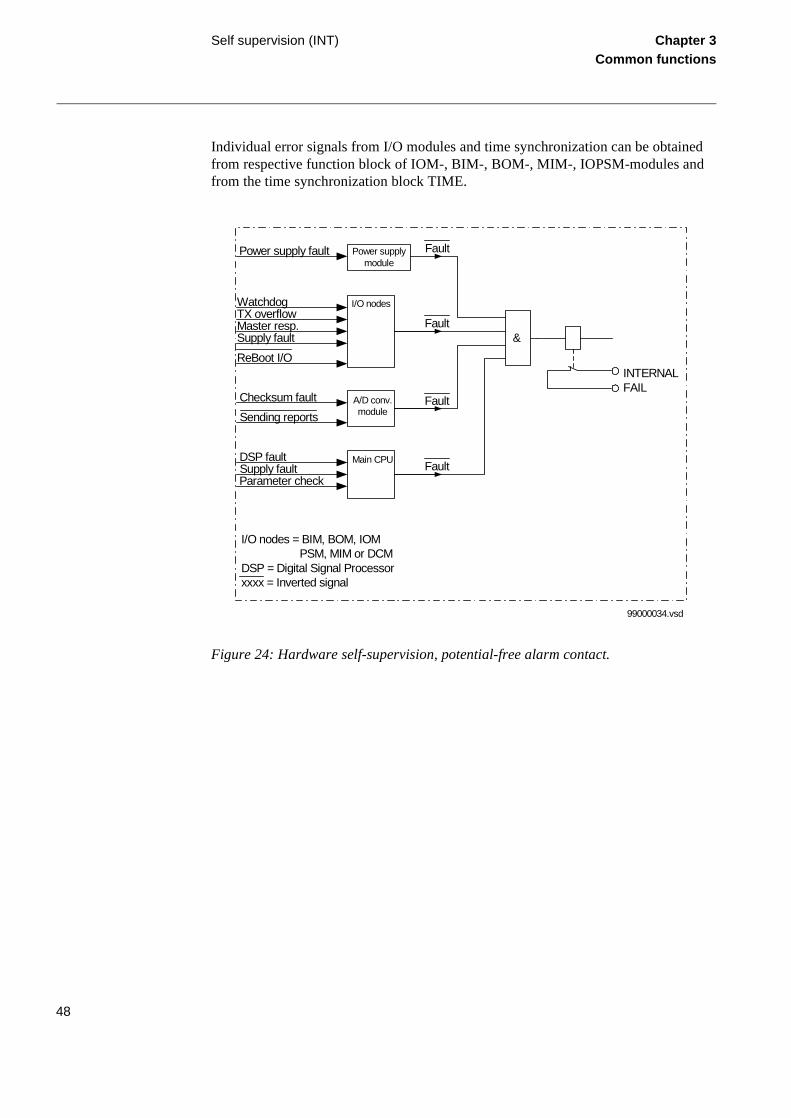
A self-supervision summary can be obtained by means of the potential free alarmtact located on the power supply module. The function of this output relay is an Ofunction between the INT--FAIL signal (figure 25) and a couple of more severe fathat can happen in the terminal (figure 24).
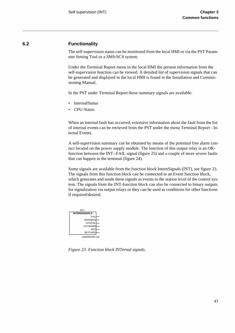
Some signals are available from the function block InternSignals (INT), see figureThe signals from this function block can be connected to an Event function blockwhich generates and sends these signals as events to the station level of the contem. The signals from the INT-function block can also be connected to binary oufor signalization via output relays or they can be used as conditions for other funcif required/desired.
Figure 23: Function block INTernal signals.
xx00000169.vsd
INT--INTERNSIGNALS
FAILWARNING
CPUFAILCPUWARN
ADCSETCHGD
47
Self supervision (INT) Chapter 3Common functions
Individual error signals from I/O modules and time synchronization can be obtained from respective function block of IOM-, BIM-, BOM-, MIM-, IOPSM-modules and from the time synchronization block TIME.
Figure 24: Hardware self-supervision, potential-free alarm contact.
Power supply fault
WatchdogTX overflowMaster resp.Supply fault
ReBoot I/O
Checksum fault
Sending reports
DSP faultSupply faultParameter check
Power supplymodule
I/O nodes
A/D conv.module
Main CPU
&
Fault
Fault
Fault
Fault
INTERNALFAIL
I/O nodes = BIM, BOM, IOM PSM, MIM or DCMDSP = Digital Signal Processorxxxx = Inverted signal
99000034.vsd
48
Self supervision (INT) Chapter 3Common functions
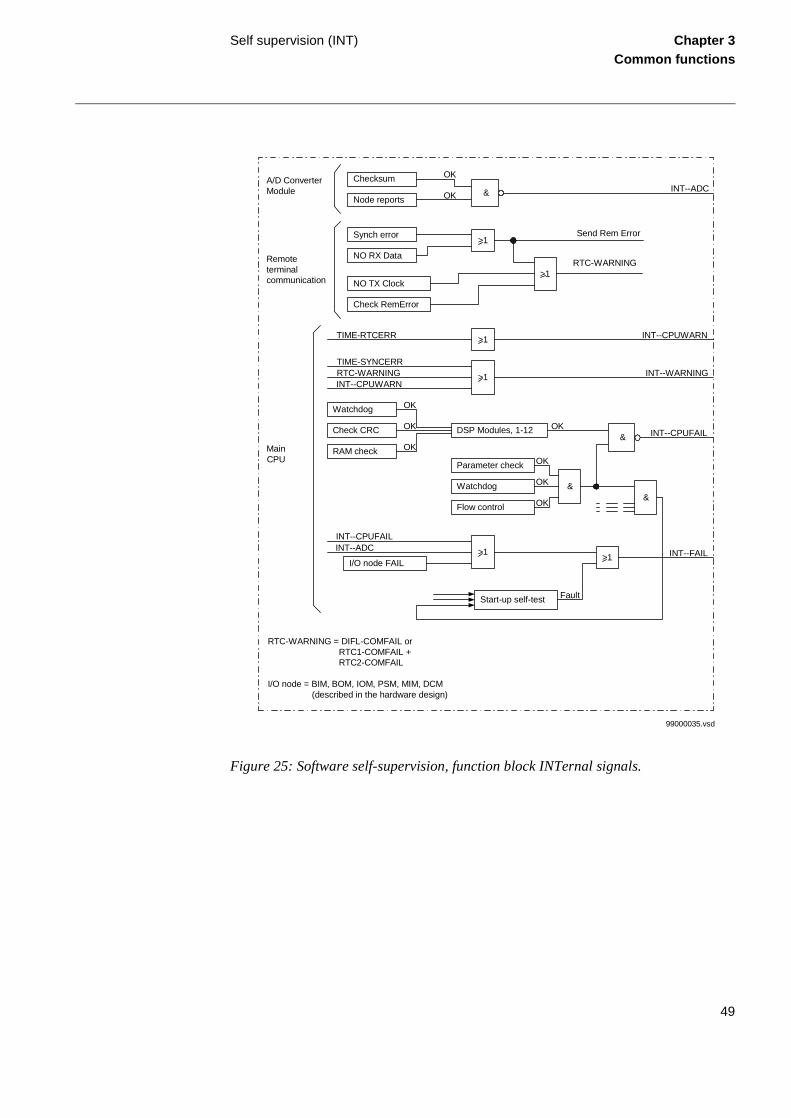
Figure 25: Software self-supervision, function block INTernal signals.
Checksum
Node reports
Synch error
NO RX Data
NO TX Clock
Check RemError
&
>1
>1
INT--ADC
Send Rem Error
OK
OK
>1TIME-RTCERR INT--CPUWARN
>1
TIME-SYNCERRRTC-WARNINGINT--CPUWARN
INT--WARNING
Watchdog
Check CRC
RAM check
DSP Modules, 1-12
OK
OK
OK&
OKINT--CPUFAIL
Parameter check
Watchdog
Flow control
&
OK
OK
OK&
>1
INT--CPUFAILINT--ADC
I/O node FAILINT--FAIL
Start-up self-test Fault
MainCPU
Remoteterminalcommunication
A/D ConverterModule
RTC-WARNING = DIFL-COMFAIL or RTC1-COMFAIL + RTC2-COMFAIL
I/O node = BIM, BOM, IOM, PSM, MIM, DCM (described in the hardware design)
99000035.vsd
>1
RTC-WARNING
49

Blocking of signals during test Chapter 3Common functions
7 Blocking of signals during test
7.1 Functionality
This blocking function is only active during operation in the test mode, see example in Figure 26. When exiting the test mode, entering normal mode, this blocking is disabled and everything is set to normal operation. All testing will be done with actually set and configured values within the terminal. No settings etc. will be changed. Thus no mis-takes are possible.
The blocked functions will still be blocked next time entering the test mode, if the blockings were not reset.
The blocking of a function concerns all output signals from the actual function, so no outputs will be activated.
Each of the terminal related functions is described in detail in the documentation for the actual unit. The description of each function follows the same structure (where appli-cable).
50
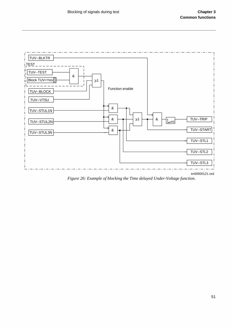
Blocking of signals during test Chapter 3Common functions
Figure 26: Example of blocking the Time delayed Under-Voltage function.
TUV--BLKTR
TUV--BLOCK
TUV--TEST
Block TUV=Yes
TUV--STUL1N
TUV--STUL2N
TUV--STUL3N
&
>1 & TUV--TRIP
TUV--START
TUV--STL1
TUV--STL2
TUV--STL3
TEST
TUV--VTSU
>1
&
&
&
en00000121.vsd
Function enable
t
51

Blocking of signals during test Chapter 3Common functions
52

About this chapter Chapter 4Line differential
Chapter 4 Line differential
About this chapter
This chapter describes the line differential functions in the terminal.
53
Line differential protection (DIFL) Chapter 4Line differential
2 ms, e.
upted
1 Line differential protection (DIFL)
1.1 Application
The line differential protection function can be used on two-terminal-lines. It can be ap-plied on MV, HV as well as on EHV overhead lines and cables. The measurement is phase segregated, which gives correct phase selection for all types of faults, including simultaneous faults on double circuit lines and faults between lines at different voltage levels.
The differential protection is neither affected by voltage and current reversal at series compensated systems, nor by harmonics produced by HVDC or SVC installations. Un-equal CT ratio in the two line ends can be compensated for.
Two binary signals can be exchanged between the terminals. The signals can be persis-tent, when used for other than tripping purposes.
The differential protection requires a 56/64 kbit/s digital communication link, which can be achieved either by dedicated optical fibres or by multiplexed channels. Commu-nication is required in both directions.
The line differential function in the protection of version 2.3 is compatible with earlier versions 1.1, 1.2 and 2.0.
The maximum transmission time for which the differential function will operate is 12 ms. For longer transmission times, the differential function will be blocked and an alarm “Communication Failure” will be given. The tripping function will not be blocked at route switching, as long as the communication time is in the range of 1neither will a false operation be caused by any changes in the communication tim
The exchanged message is controlled by added check-sum information and corrtelegrams are not evaluated.
Note!
Transformers or tapped loads in the protected zone are normally not allowed.
54
Line differential protection (DIFL) Chapter 4Line differential
r to cation hard-chapter
iltered iour. At e sat-
e trans-
1.2 Functionality
The Line differential function offers phase-segregated true current differential protec-tion for transmission, subtransmission and distribution networks. The function com-pares the currents entering and leaving the protected overhead line or cable. This is done by exchanging the value of the three phase currents in both directions every 5 ms, inte-grated in a common digital message. The currents are evaluated in both terminals on a per phase basis that prevents the problem of the current summation approach and pro-vides phase selection information for single-pole tripping. The operating characteristic is shown in figure 28.
A dependable communication link is needed to allow exchange of the current informa-tion between the terminals at the line ends. Direct optical fiber or galvanic commnica-tion link are supported, as well as more complex digital communication systems like multiplexed and route switched networks.The transmission time is continuously mea-sured to provide correct synchronization of local clocks.
Two independent binary signals can be transmitted from one line side to the other through the differential communication link for direct intertrip logics or information purposes.
The Line differential function uses the same communication functionality and hardware for communication with remote end as used for the function “Binary signal transfteremote end (RTC)”. These items are described in the Remote end data communichapter for the software and in the Digital communication module chapter for the ware. The settings that has to be made for these items are also desribed in each respectively.
In figure 27 a simplified block diagram of the line differential protection function isshown.
Patented saturation detectors evaluate each phase current locally, utilising the unfsamples issued every ms. The detection is based on the secondary current behavcurrent transformer saturation, the stabilisation is increased at both terminals in thurated phase. Therefore, phase segregated “saturation” signals are included in thmitted message.
55
Line differential protection (DIFL) Chapter 4Line differential
Figure 27: Simplified block diagram, line differential protection function
7
8
1≥
DIFL-BLOCK
1≥
DIFL-RTCSEND1DIFL-RTCSEND2
Idiff
Ibias
56
DIFL-CTSAT
DIFL-BLOCK
4
DIFL-RTCREC1DIFL-RTCREC2
DIFL-TRIP
2
DATA TRANSMITDATA RECEIVE1
1≥
3
en01000087.vsd
I
Where:
1 Communication interface
2 Communication logic
3 Remote trip
4 Remote current value
5 Remote saturation detection
6 Remote block
7 Fourier filter
8 Saturation detector
56
Line differential protection (DIFL) Chapter 4Line differential
Figure 28: Stabilisation characteristic.
Where:
IMinOp Minimum differential operation current
IMinSat Minimum phase current for saturation detection operation
IDiffLvl1 Slope 1 stabilisation
IDiffLvl2 Slope 2 stabilisation
ILvl1/2Cross Slope 2 intersection
57

Line differential protection (DIFL) Chapter 4Line differential
1.3 Design
General
The line differential function is designed to work with digital communication systems. To ensure compatibility with a wide range of communication equipment and media, the relay is designed to work within the signalling bandwidth of a standard CCITT PCM channel at 64 kbits/s. To enable the use in North American EIA PCM systems working at 56 kbits/s, some of the interfacing modules can be adapted to this bit rate.
Current differential function
This section describes the filtering used for the Line differential function and the eval-uation of the local and remote current based on these filter values.
Current filtering
The phase currents are sampled with 2000 Hz sampling frequency. Of two consecutive samples, one sample is achieved after an interpolation to achieve a set of samples relat-ed to the same instant (skew adjustment). After the interpolation, one set of samples is achieved every ms. The phase currents are Fourier filtered, and the fundamental (50/60 Hz) component in the current, is represented with the Fourier coefficients a and b, see equation 15 and equation 16. The Fourier filters produces a set of a and b coefficients every ms. These coefficients represent the sin and cos components, related to a local fundamental frequency reference.
Note!
A safe and reliable operation of the differential function requires the transmission timeto be equal in both directions between the two terminals. If the transmission time in thetwo directions not equal this will produce a false differential current that is load currentmultiplied by sine of the angle corresponding to half the transmission time difference.A 1 ms difference will create a differential current that is 16% of load current at 50 Hzand 19% at 60 Hz.
For negligible influence the difference in transmission time must be less than 0.2 ms.
For further information see section "Time synchronization", especially section "Effectof unequal transmission time delay".
Note!
The maximum transmission time for which the differential function will operate is12 ms. For longer transmission times, the differential function will be blocked and analarm “Communication Failure” will be given.
58

Line differential protection (DIFL) Chapter 4Line differential
d in rder
special ot the Fou- the
s of nchro-s per-s
(Equation 15)
(Equation 16)
The transmitted current information to the remote end consists of the a and b coeffi-cients. These coefficients carry the entire amplitude and phase angle information. For a static current, the coefficients do not change their value during the cycle. During dy-namic conditions, the “primary” current changes, and thus also a and b change with time.
Due to the design of the A/D-converters, the primary sampling is not synchronizethe terminals at the two ends of the line and thus neither is the Fourier filtering. In oto be able to compare current values taken at the same instant at the two ends a algorithm has been included. This consists of a reference clock in each terminal, nsame as used for the Fourier filtering, together with a time skew adjustment of therier filter outputs. The mechanism for synchronizing the clocks in the terminals attwo line ends are described later on.
The a and b coefficients for the three phase currents are transmitted every even 5 mthe reference clock, that is at 0 ms, 5 ms, 10 ms etc. Since the sampling is not synized to the reference clock a linear interpolation to an even 5 ms time instance iformed between a set of a and b coefficients taken immediately before the even 5 mand a set of a and b coefficients taken immediately after, see figure 29.
Iphase f t( ) f ωf( ) f ω ωf≠( )+= =
f ωf( ) a sin ωft⋅ b cosωft⋅+=
59
Line differential protection (DIFL) Chapter 4Line differential
nts
Figure 29: Interpolation of a and b
The reference clock is actually a 0 to 39999 microsecond timer. Samples shall be sent every even 5 ms, that is every n*5 ms there n is an integer 0,1, 2..., 7. This corresponds to a phase angle ϕc = n*1.8*fn there fn is the set frequency of the terminal. When the sample is to be sent the phase angle of the reference for the Fourier filter ϕf is checked. These two phasors will create two coordinate systems according to figure 30. The a and b coefficients from the Fourier filter uses FR as reference. To be able to compare cur-rents from the two ends the a and b coefficients have to be referenced to the reference clock common for the two terminals, that is CR. In order to do that the output from the Fourier filter is rotated with an angle according to equation 17 creating a new set of co-efficients, a’ and b’. The transmitted data consists of the set of these new coefficie a’ and b’ together with the n value mentioned above for which they were calculated.
(Equation 17)
Value
Value at t
Value to be sent
Value at t + 1 ms
t
Even 5 ms
t + 1 ms Time
en01000132.vsd
a’ jb’+ a jb+( )eϕf ϕc–( )–
=
aa’
bb’
ϕc
ϕf
FR
I
CR
en01000141.vsd
60

Line differential protection (DIFL) Chapter 4Line differential
nes. tect the her be will pera-r Data
is faults ental to alue eme s are y is ime
e trip- the he iza-mu-
d in-lection
Figure 30: Fourier filter coefficient transformation
At the evaluation, the received a’ and b’ coefficients are compared with the locally cal-culated a’ and b’ coefficients that are related to the same n value as the received oThe data messages that are transmitted every 5 ms also contain check bits to defalse information. A message that does not pass the check is rejected and will neitevaluated for tripping nor used for synchronization of the clocks. A new messagebe received 5 ms later. When a message is rejected during an internal fault, the otion time is prolonged by 5 ms. The design of the messages is described in chaptecommunication.
By utilizing Fourier filtering, the influence of non-fundamental frequency currentsreduced. The inrush current when energizing and the outfeed current at external caused by the capacitive stored energy in the line, are dominated by non-fundamfrequency components. The minimum operating current must be set high enoughachieve stability at these two conditions. The filtering allows a lower set operating vthan unfiltered quantities would allow. The use of Fourier quantities makes the schindependent of the communication link time delay, as long as the reference clocksynchronized or the time difference is known. Therefore, the communication delaof interest only for the synchronization of local clocks. Naturally, the transmission tis added to the basic operating time.
Owing to this design, the measurement does not need to be blocked to avoid falsping when the communication delay is changed. The protection will be blocked ifcommunication delay cannot be identified within 200 ms, due to disturbances in tcommunication. The stability of the local clocks allows operation without synchrontion for a time period of more than 200 ms. If the protection is blocked due to comnication disturbances, the protection is automatically deblocked when the communication is established and the local clocks are synchronized again.
Current evaluation
The differential protection evaluation is carried out in both terminals and performedividually for each phase. By using phase segregated evaluation, correct phase seis achieved for any type of fault.
Where:
I Phase current
FR Fourier filter reference
CR Master/slave reference clock
61
Line differential protection (DIFL) Chapter 4Line differential
At the evaluation, a differential and a bias current are calculated for each phase by vec-torial and scalar summation of the local and remote currents, represented by the a’ and b’ coefficients. The scalar sum is divided by two in order to achieve the bias current. The differential and bias values are calculated for each phase according to equation 18 and equation 19.
(Equation 18)
(Equation 19)
The value for IDiff is then used directly when evaluating differential and bias values against characteristic while for bias following value, equation 20, is calculated and used for each phase:
(Equation 20)
The differential and bias currents are compared and a trip situation is indicated in the phases where the differential current is above the characteristic according to Figure 31. For tripping, 2 or 3 out of 4 consecutive measurements are required to indicate a trip. The selection between the required 2 or 3 evaluations is user selecctable.
The minimum operate current (IMinOp), the two slopes (IDiffLvl1 and IDiffLvl2) and the intersection between slope 1 and 2 (ILvl1/2Cross) can be set. This characteristic takes care of the measuring errors in the primary current transformer and the protection, when the current transformer is not saturated. At current transformer saturation, the sta-bilization is increased in both terminals in the saturated phase, see Figure 31. Therefore, phase segregated “saturation” signals are included in the transmitted message.
IDiff ILocal IRemote+=
IBias
ILocal IRemote+
2-------------------------------------------=
IBias( ) Evaluate Max IBias( ) Own phase[ ] OR 0.5 IBias( )Other phases⋅[ ] =
Note!
IMinSat is not set, nor evaluated, as a percentage of IBias but as a percentage of I1b andevaluated on a phase current base. It is therefor not mathematically correct to show IM-inSat in the IDiff/IBias diagram but this is done due to that the slope has to be shown inthe diagram.
62
Line differential protection (DIFL) Chapter 4Line differential
Figure 31: Stabilization characteristic.
Saturation detector
A patented saturation detectors evaluate each phase current locally, utilizing the unfil-tered samples issued every ms. The detection is based on the secondary current behav-iour. In case of a saturation, the current decreases abruptly, from a high amplitude value to a low one, followed by a low rate of change. This condition is checked by means of three consecutive current samples, at t-2, t-1 and t, according to figure 32.
63
Line differential protection (DIFL) Chapter 4Line differential
Figure 32: CT-Saturation Detector
A saturation is detected if the conditions in equations 21 to 9 are fulfilled. Ipeak is the maximum current since last zero crossing. IMinSat is a setting. It should be noted that equation 21 is based on sample value, the value Ipeak is actually compared with √2×IM-inSat.
(Equation 21)
(Equation 22)
(Equation 23)
en01000139.vsd
CT saturation detected
t-2 tt-1
Ipeak
IPeak IMinSat≥
I t 2–( ) I t 1–( )–[ ] K3 IPeak⋅≥
I t 1–( ) I t( )–[ ] K2 IPeak⋅≤
64
Line differential protection (DIFL) Chapter 4Line differential
ither
(Equation 24)
Equation 21 indicates that the current must have been above IMinSat since last zero crossing. Equation 22 means that the slope of the current between t-2 and t-1 must be higher than a certain factor of Ipeak. Equation 23 means that the slope of the current be-tween t-1 and t must be lower than a certain factor of Ipeak. Equation 24 means that the current value at t must be lower than a certain factor of Ipeak.
The use of saturation detectors enables minimum current transformer requirements, to-gether with maximum sensitivity.
Time synchronization
The communication link delay measurement and synchronization of internal clocks in the line differential function is an essential part of the successful operation of the func-tion. In this section is described:
1. transmission time measurement,
2. clock synchronization and
3. compensation for differences in oscillator frequency.
The time synchronization is based on a master-slave concept not to be mixed up with the master-master concept used for current evaluation. At the time synchronization, the slave synchronizes its internal clock in the line differential function (not the real time clock used for time tagging of events etc) to the master.
Transmission time measurement
The transmission time is measured by comparing local send and receive times for mes-sages transmitted between the two terminals, the master and the slave, the so-called ping-pong method. The messages are normally transmitted at a rate of one every 5 ms. The clock used for time tagging these messages is not linked to the absolute time in the terminals, used for example for time tagging of events etc. Instead it is based on a 0 to 39999 microsecond internal clock in the differential function which has a resolution of 1 µs which is controlled by the oscillator for the CPU.
The maximum transmission time for which the differential function will operate is 12 ms. For longer transmission times, the differential function will be blocked and an alarm “Communication Failure” will be given. The tripping function will not be blocked at route switching, as long as the communication time is within 12 ms, newill a false operation be caused by any changes in the communication time.
I t( ) K1 IPeak⋅≤
65
Line differential protection (DIFL) Chapter 4Line differential
In figure 33 it is shown how a message is sent from the slave to the master and another from the master to the slave. The message from the slave is sent at time t1. This time is stored at the slave. The message is received at the master at the time t2. The time a mes-sage is sent is taken as the time when the last bit of the message is sent, last bit of stop flag, and the time a message is received is taken as the time the last bit of the stop flag is received.This time is stored in the master and sent to the slave by the following mes-sage at time t3. This time is stored in the master and sent to the slave by the following message. The first message is received at the slave at the time t4. This time is stored at the slave. Taking into consideration the difference ∆t between the clocks in the two ter-minals and the time it takes for a message to be transmitted from one terminal to the other, Td, the associations in equations 25 and 26 can be set up.
Figure 33: Exchange of messages between slave and master
(Equation 25)
(Equation 26)
To insure that the times t1, t2 and t3, t4 respectively belongs to the same message, each message is given a number which is stored and transmitted together with the message. After the time t3 has been received by the slave, the slave will combine the four times and calculate the transmission time, Td, in the communication link, assuming that the transmission time is equal in both directions. The equation for this is according to equa-tion 27.
Master
Slave
∆t
0t1
0
Tdt4
t3t2
en01000133.vsd
t2 t1 Td t∆–+=
t4 t3 Td t∆+ +=
66
Line differential protection (DIFL) Chapter 4Line differential
(Equation 27)
The assumption that the transmission time is equal in both directions depends on the fact that with knowledge of only the four times mentioned above it is possible only to determine two unknown variables, in this case the total transmission time and the dif-ference ∆t between the two clocks. If the difference would be known it would instead be possible to determine the transmission time in each direction. From equation 27 it can further be seen that any difference between the clocks in the slave and master will not effect the calculation of Td since both times within each bracket is only local times.The value Td calculated for the transmission time is not used directly in the algo-rithm for synchronizing the clocks in the slave and master or time adjustment of sam-ples but only for controlling the stability of the communication channel and that it is within the maximum allowable transmission time of 12 ms.
Clock synchronization
If the clocks in the slave and master were synchronous t2 should be equal to t1 + Td. Now assume that there are a small difference ∆t, according to figure 33, between the two clocks. This can, with the above equation, be calculated according to equation 28.
(Equation 28)
The first term in equation 28 is actually the midpoint between t1 and t4 and the second is the midpoint between t2 and t3. ∆t will therefor be the difference between these two midpoints which will be independent on the transmission time as long as the transmis-sion time is equal in both directions. If the clock in the slave is leading the clock in the master ∆t will be >0 and if the clock in the slave is lagging the clock in the master ∆t will be <0. Before any compensation for ∆t is performed, it is checked that the trans-mission time Td has been constant for some time and is shorter than maximum value, that is 12 ms. If this is fulfilled the clock in the slave is adjusted by a certain time ta, positive or negative depending on the sign of ∆t. The time ta is function of the mean value of ∆t for a number of messages and also on the time the communication has been lost. It can be expressed as in equation 29.
Td
t4 t1–( ) t3 t2–( )–
2---------------------------------------------=
t∆t1 t4+
2---------------
t2 t3+
2---------------–=
67
Line differential protection (DIFL) Chapter 4Line differential
(Equation 29)
The dependence on time of lost communication has the purpose of speeding up the syn-chronization at terminal start up when the difference between the two clocks can be big. If during this process a shift in Td is recognized the adjustment will be stopped until Td again has been constant for a certain time. During a synchronization after terminal start up or if the communication has been interrupted for a number of minutes the differential protection is blocked until the mean value of ∆t is below a certain level which can take up to a minute. Since it is only the slave that measures the difference between the two clocks, a block signal is sent from the slave to the master with every message until the slave is synchronized. If the two clocks are synchronized, the clock of the slave will be continuously adjusted up and down depending on the sign of the mean value of ∆t with a very small time ta since it is impossible to keep the two clocks exactly synchronized due to for example differences in the oscillators for the CPU in the slave and the master. If a shift in Td is recognized the adjustment will be stopped as mentioned above until Td again has been constant for a certain time. However since the two clocks were al-ready synchronized they will keep on being synchronized for a long time, actually up to tens of minutes, due to the precision of the oscillators and therefor the protection can keep on working. As mentioned above, change in transmission time has no effect on the synchronization between the two clocks and therefor it is not needed to know the exact transmission time only that it is not changing and not too long. For safety reasons the protection will however be blocked if Td is unstable for more than approximately 200 ms due to uncertain communication. When Td becomes stable again the process de-scribed above will take place and, if the time of unstable communication has not been long, the clocks will probably still be rather well synchronized so the synchronization procedure will be much faster, normally less than one second before the protections are released again.
Where:
∆t(n) is measured time difference for message n,
c is the number of messages for which the mean value of the time differ-
ence is calculated and
tL is the time the communication has been lost.
ta f t∆ n( )n 1=
c
∑
c tL,( )⁄
=
68
Line differential protection (DIFL) Chapter 4Line differential
ed by cy. If ils. wo as e be
f
ith hould en-tion
Effect of unequal transmission time delay
If the transmission times in the two directions, slave to master and master to slave, are not equal this will produce an error in the current measurement. Assume a difference in transmission time of ∆Td. This will lead to an additional term in equation 28 of -∆Td/2.
This will lead to that the compared Fourier values will be taken with a -∆Td/2 ms dif-ference between the two ends. During steady state conditions this will have the effect that a differential current is created with an amplitude of ILoad x sin(∆Td x 180 x f) there ILoad is the load current on the line and f is the network frequency. ∆Td is measured in seconds.During changes in currents, both amplitude and phase, the a and b values will change with time and this will create a somewhat higher differential current than the steady state condition.
The only way of avoiding malfunction, if unequal transmission times are a fact, is to set IMinOp, IDiffLvl1 and IDiffLvl2 higher than expected “false” differential current.
Compensation for differences in oscillator frequency
As mentioned above the clocks that are used for the synchronization are controllthe oscillators for the CPU. As for all components also these have some inaccuranothing is done to this the two clocks will slowly drift apart if the communication faThe rate of this drift will depend on the magnitude of the difference between the toscillators. In order to minimize this drift a method for compensating for the drift hbeen implemented. The principle is as follows. Let the adjustment at a certain timta(n). Measure ta for some number N of messages. Create the signal ∆tosc according to equation 30.
(Equation 30)
If the two oscillators have exactly the same frequency, ∆tosc will be 0. If there exists a difference between them ∆tosc will get a value that is equal to the drift in the clock othe slave compared to the master between two adjustments. The value of ∆tosc is stored in the CPU and used for regular additional adjustment of the clock in the slave. Wthis compensation the drift can be decreased to only some percentage of what it sbe without compensation, normally less than 10 ppm compared to 100 ppm. Thissures that the system can operate for quite a long time also without a communicachannel stable enough for synchronization.
tosc∆ tan 1=
N
∑ n( )
N⁄=
69

Line differential protection (DIFL) Chapter 4Line differential
Data message
A data message is sent every 5 ms. The message is based on the HDLC protocol. For more details, see chapter Data communication.
1.4 Calculations
1.4.1 Setting instructions
General
All configuration is performed with CAP 531, the graphical configuration tool. Settings are done according to the following sections.
Selection of protection parameters
The secondary current that is to be compared in both terminals, must be related to a common current transformer ratio. With a CTFactor default setting of 1.00, this is achieved when the current transformers at both terminals have the same rated primary current. When one of the terminals has a higher primary rated current than the other, this can be numerically equalised by the CTFactor setting. By setting the CTFactor in the terminal with the higher primary rated current to the quote between the lower and the higher rated current, the difference is equalised. The nominal primary current for the whole differential protection function (Inominal), to which all function data is related, is the lower rated current.
If the primary rated current is much higher than the maximum load current, the differ-ential nominal current (Inominal) can be reduced by the CTFactor at both terminals. In this case, the nominal primary current (Inominal), to which all function data is related for the differential protection, is equal to the rated primary current multiplied by the CT-Factor.
Identical settings for IMinOp, IDiffLvl1, IDiffLvl2, ILvl1/2Cross and IMinSat should be used at both terminals.
The minimum operating current, IMinOp, is chosen in relation to the fundamental fre-quency charging current. The primary minimum operating current must not be lower than 2.5 times the total charging current (practically, the charging current when the line is fed from only one terminal).
When current transformers of the same type are used at both terminals, and they are di-mensioned according to, “Requirements and technical data”, the default settings:IDiffLvl1=20% of IBias, IDiffLvl2=50% of IBias and ILvl1/2Cross=500% of IBias are applied.
70
Line differential protection (DIFL) Chapter 4Line differential
ex-e-
e com-ng,
enu
pond-
ction
the
e-d
other
ail-
The IDiffLvl is increased to 160% of IBias at detected saturation. With current trans-formers dimensioned according to “Requirements” the default value IMinSat=300% of IBias is used. The meaning of this is that the magnitude of the current must haveceeded 3 times the base current (Ib) within the previous half cycle, for the saturation dtector to be released. When the current transformer margin E2max>3 times, the minimum requirement, the IMinSat can be increased to 500%.
By setting the Evaluate 2 of 4 instead of the default setting 3 of 4, the operating timcan be reduced by 5 ms. The setting 2 of 4 is recommended only when high qualitymunication is used. The reason for this is the slightly increased risk of false trippidue to corrupt messages.
The setting parameters for the differential protection function are available in the mtree in the local HMI under the menu:
Setting
Function
Group n
Differential
For remote setting and local HMI via personal computer, please refer to the corresing SMS or SCS documents.
Line differential protection communication
To make sure that the differential protection communicates with the correct proteat the opposite terminal, the terminals are numbered. By giving all differential protec-tions transmitting over a common multiplexer individual identification numbers, com-munication with the wrong terminal can be avoided. The terminals are given identification numbers 0-255 by a setting parameter. The identification number ofopposite terminal must also be set. This is always necessary.
TerminalNo is the identification that is sent with the message to the remote end. RmoteTermCom is the identification aganinst which the identification of the receivemessage is checked to see that the message orginates from correct terminal.
For the synchronisation of the local clocks, one terminal has to be master, and theone slave.
The configuration parameters for the differential protection communication are avable in the menu tree in the local HMI under:
71

Line differential protection (DIFL) Chapter 4Line differential
Configuration
DiffFunction
and
Configuration
TerminalCom
RemTermCom
72

About this chapter Chapter 5Current
Chapter 5 Current
About this chapter
This chapter describes the current protection functions.
73
Instantaneous overcurrent protection (IOC)
Chapter 5Current
power
ase
rators ts if the
and tion , for
otec-lts efer
lts in he se are
1 Instantaneous overcurrent protection (IOC)
1.1 Application
unbalanceLong transmission lines often transfer great quantities of electrical power from production to consumption areas. The unbalance of the produced and consumed electrical power at each end of the transmission line is very large. This means that a fault on the line can easily endanger the stability of a complete system.
The transient stability of a power system depends mostly on three parameters (at con-stant amount of transmitted electrical power):
• The type of the fault. Three-phase faults are the most dangerous, because no can be transmitted through the fault point during fault conditions.
• The magnitude of the fault current. A high fault current indicates that the decreof transmitted power is high.
• The total fault clearing time. The phase angles between the EMFs of the geneon both sides of the transmission line increase over the permitted stability limithe total fault clearing time, which consists of the protection operating time andbreaker opening time, is too long.
The fault current on long transmission lines depends mostly on the fault position decreases with the distance from the generation point. For this reason the protecmust operate very quickly for faults very close to the generation (and relay) pointwhich very high fault currents are characteristic.
For this reason instantaneous, non-directional, phase-segregated, overcurrent prtion (IOC), which can operate in 15 ms (50 Hz nominal system frequency) for faucharacterized by very high currents, is included in some of the REx 5xx terminals. Rto the ordering information for more details.
The conventional distance protection can manage the fault clearance of earth-faumost of the cases. In some applications, especially applications with long lines, tclearance can be improved by use of an instantaneous earth-fault protection. Thofor instance:
74
Instantaneous overcurrent protection (IOC)
Chapter 5Current
ight instan-
t the in a ce.
ng fault
ction clear-
can ry
in-
con-> set
ignal ase
the
con-alue.
vents e out-se-
own
• In the case of high infeed of fault current from the opposite end of the line, this mincrease the fault resistance seen by the distance relay to such a value that thetaneous step of the distance protection will not operate.
• In applications with series compensated lines, where the capacitor is located aend of the line and very strong infeed of fault current from that end, will result difficult problem for the distance protection to perform a selective fault clearanThis due to the voltage reversal that might occur.
The use of instantaneous overcurrent earth-fault protection is most suitable for lolines in meshed transmission systems. It can also be used for radial lines with lowcurrent infeed from the opposite end of the line.
The instantaneous residual overcurrent function is very suitable as back-up protefor phase to earth faults close to the terminal. This enables a short back-up faultsance time for the phase to earth faults with high fault current.
The instantaneous, non-directional, earth-fault overcurrent protection (IOC), whichoperate in 15 ms (50 Hz nominal system frequency) for faults characterized by vehigh currents, is included in some of the REx 5xx terminals. Refer to the orderingformation for more details.
1.2 Functionality
The current-measuring elements within one of the built-in digital signal processorstinuously measure the current in all three phases, and compare them with the IP>value. The logical value of each phase current signal on the output of the digital sprocessor (STIL1, STIL2 and STIL3 respectively) is equal to 1 if the measured phcurrent exceeds the preset value.
The measuring technic is based on measuring of the incoming residual current toterminal.
The current-measuring elements within one of the built-in digital signal processorstinuously measure the zero sequence current, and compare it with the IN>> set vA recursive Fourier filter filters the current signals, and a separate trip counter prehigh overreaching of the measuring elements. The logical value of the signal on thput of the digital signal processor (IOC--STIN) is equal to 1 if the measured zero quence current exceeds the pre-set value.
1.3 Design
The simplified logic diagram of the instantaneous phase overcurrent function is shin figure 34.
75
Instantaneous overcurrent protection (IOC)
Chapter 5Current
en
ent lock nc-ns.
out-func-
g sig-. ut sig-
to h sin-
The overcurrent function is disabled if:
• The terminal is in TEST mode (TEST-ACTIVE is high) and the function has beblocked from the HMI (BlockIOC=Yes)
• The input signal IOC--BLOCK is high.
The IOC--BLOCK signal is a blocking signal of the instantaneous phase overcurrfunction. It can be connected to a binary input of the terminal in order to receive a bcommand from external devices or can be software connected to other internal futions of the terminal itself in order to receive a block command from internal functioThrough OR gate it can be connected to both binary inputs and internal function puts. The IOC--BLOCK signal blocks also the instantaneous residual overcurrent tion, if this is installed in the terminal.
When the instantaneous phase overcurrent function is enabled, the output trippinnals IOC--TRL1, IOC--TRL2, IOC--TRL3, IOC--TRP and IOC--TRIP can operateThe duration of each output signal is at least 15 ms. This enables continuous outpnals for currents, which go just a little above the set operating value.
The single phase trip signals IOC--TRL1, IOC--TRL2, and IOC--TRL3 are relatedL1, L2, and L3 phases and therefore also suitable for the single phase tripping witgle-phase auto-reclosing.
76

Instantaneous overcurrent protection (IOC)
Chapter 5Current
Figure 34: Simplified logic diagram of instantaneous overcurrent protection
The signal IOC--TRP is the logic OR of the three single phase trips. It can be used to trip the circuit breaker if only three phase operation is desired.
The IOC--TRIP output signal behaves as general instantaneous overcurrent trip when in the REx 5xx terminal also the instantaneous residual overcurrent function is imple-mented; i.e. this signal will be activated in case of any single phase overcurrent or re-sidual overcurrent detection. If only the instantaneous phase overcurrent function is installed in the terminal, then this signal behaves exactly as the signal IOC--TRP and can be used for signalization.
The simplified logic diagram of the instantaneous phase overcurrent function is shown in figure 35.
The overcurrent function is disabled if:
IOC--BLOCK
IOC--TRIP
en01000077.vsd
&
Function Enable
IOC - INSTANTANEOUS PHASE OVERCURRENT FUNCTION
>1
STIL1
&
&
&
&
STIL2
STIL3
IOC--TRP
IOC--TRL1
IOC--TRL2
IOC--TRL3
>1
TEST-ACTIVE&
TEST
BlockIOC = Yes
77
Instantaneous overcurrent protection (IOC)
Chapter 5Current
een
on-es or rmi-R
nd en-g val-
when le-or in -he d for
• The terminal is in TEST status (TEST-ACTIVE is high) and the function has bblocked from the HMI (BlockIOC=Yes)
• The input signal IOC--BLOCK is high.
The IOC--BLOCK signal is a blocking signal of the overcurrent function. It can be cnected to a binary input in order to receive a block command from external devicit can be configured (software connection) to other internal functions within the tenal itself, in order to receive a block command from internal functions. Through Ogates it can be connected to both binary inputs and internal function outputs.
When the overcurrent function is enabled, the output tripping signals IOC--TRN aIOC--TRIP can operate. The duration of each output signal is at least 15 ms. Thisables continuous output signals for currents, which go just beyond the set operatinue.
The IOC--TRN signal is related to the residual overcurrent trip.
The IOC--TRIP output signal behaves as general instantaneous overcurrent trip in the REx 5xx terminal also the instantaneous phase overcurrent function is impmented. I.e. this signal will be activated in case of residual overcurrent detection case of any single-phase overcurrent detection (IOC--STIL_: IOC--STIL1 or IOC-STIL2 or IOC--STIL3). If only the residual overcurrent function is implemented in tterminal, then this signal behaves exactly as the signal IOC--TRN and can be usesignalising.
78

Instantaneous overcurrent protection (IOC)
Chapter 5Current
Figure 35: Simplified logic diagram of instantaneous residual overcurrent protection.
1.4 Calculations
1.4.1 Setting instructions
This protection function must operate only in a selective way. So check all system and transient conditions that could cause its unwanted operation.
Only detailed network studies can determine the operating conditions under which the highest possible fault current is expected on the line. In most cases, this current appears during three-phase fault conditions. But also examine single-phase-to-earth and two-phase-to-earth conditions.
Also study transients that could cause a high increase of the line current for short times. A typical example is a transmission line with a power transformer at the remote end, which can cause high inrush current when connected to the network and can thus also cause the operation of the built-in, instantaneous, overcurrent protection.
IOC--BLOCK
en01000078.vsd
IOC - INSTANTANEOUS RESIDUAL OVERCURRENT FUNCTION
TEST-ACTIVE&
TEST
BlockIOC = Yes
>1
&
&
IOC--STIN
IOC--TRN
IOC--TRIP
79

Instantaneous overcurrent protection (IOC)
Chapter 5Current
Meshed network without parallel line
The following fault calculations have to be done for three-phase, single-phase-to-earth and two-phase-to-earth faults. With reference to figure 36, apply a fault in B and then calculate the relay through fault phase current IfB. The calculation should be done using the minimum source impedance values for ZA and the maximum source impedance val-ues for ZB in order to get the maximum through fault current from A to B.
Figure 36: Through fault current from A to B: IfB
Then a fault in A has to be applied and the through fault current IfA has to be calculated (Figure 37). In order to get the maximum through fault current, the minimum value for ZB and the maximum value for ZA have to be considered.
Figure 37: Through fault current from B to A: IfA
The relay must not trip for any of the two trough fault currents. Hence the minimum theoretical current setting (Imin) will be:
99000474.vsd
~ ~ZA ZBZ L
A B
Relay
I fB
Fault
99000475.vsd
~ ~ZA ZBZ L
A B
Relay
I fA
Fault
80
Instantaneous overcurrent protection (IOC)
Chapter 5Current
(Equation 31)
A safety margin of 5% for the maximum protection static inaccuracy and a safety mar-gin of 5% for the maximum possible transient overreach have to be introduced. An ad-ditional 20% is suggested due to the inaccuracy of the instrument transformers under transient conditions and inaccuracy in the system data.
The minimum primary setting (Is) for the instantaneous phase overcurrent protection is then:
(Equation 32)
The protection function can be used for the specific application only if this setting value is equal to or less than the maximum fault current that the relay has to clear (IF in figure 38).
Figure 38: Fault current: IF
The current transformer secondary setting current (IsSEC) is:
(Equation 33)
Imin MAX IfA IfB,( )≥
Is 1 3, Imin⋅≥
99000476.vsd
~ ~ZA ZBZ L
A B
Relay
I F
Fault
IsSEC
ISEC
IPRIM-------------- Is⋅=
81
Instantaneous overcurrent protection (IOC)
Chapter 5Current
Where ISEC is the secondary rated current of the main CT and IPRIM is the primary rated current of the main CT.
The relay setting value IP>> is given in percentage of the secondary base current value, I1b, associated to the current transformer input I1. The value for IP>> is given from this formula:
(Equation 34)
This is the value that has to be set in the terminal.
Set this value under the setting menu:
Settings
Functions
Group n
InstantOC
Meshed network with parallel line
In case of parallel lines, the influence of the induced current from the parallel line to the protected line has to be considered. One example is given in figure 39 where the two lines are connected to the same busbars. In this case the influence of the induced fault current from the faulty line (line 1) to the healthy line (line 2) is considered together with the two through fault currents IfA and IfB mentioned previously. The maximal in-fluence from the parallel line for the relay in figure 39 will be with a fault at the C point with the C breaker open.
A fault in C has to be applied, and then the maximum current seen from the relay (IM ) on the healthy line (this applies for single-phase-to-earth and two-phase-to-earth faults) is calculated.
IP>>IsSEC
I1b--------------- 100⋅=
82
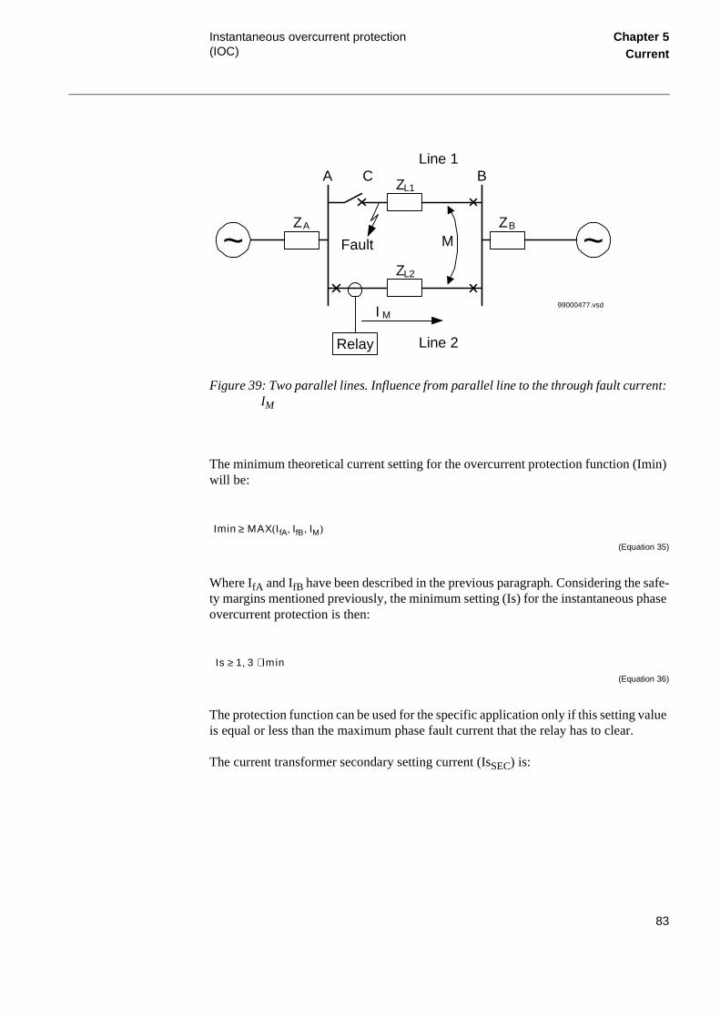
Instantaneous overcurrent protection (IOC)
Chapter 5Current
Figure 39: Two parallel lines. Influence from parallel line to the through fault current: IM
The minimum theoretical current setting for the overcurrent protection function (Imin) will be:
(Equation 35)
Where IfA and IfB have been described in the previous paragraph. Considering the safe-ty margins mentioned previously, the minimum setting (Is) for the instantaneous phase overcurrent protection is then:
(Equation 36)
The protection function can be used for the specific application only if this setting value is equal or less than the maximum phase fault current that the relay has to clear.
The current transformer secondary setting current (IsSEC) is:
99000477.vsd
~ ~ZA ZB
ZL1A B
I M
Fault
Relay
ZL2
M
CLine 1
Line 2
Imin MAX IfA IfB IM, ,( )≥
Is 1 3, Imin⋅≥
83
Instantaneous overcurrent protection (IOC)
Chapter 5Current
(Equation 37)
Where ISEC is the secondary rated current of the main CT and IPRIM is the primary sec-ondary rated current of the main CT.
The relay setting value IP>> is given in percentage of the secondary base current value, I1b, associated to the current transformer input I1. The value for IP>> is given from this formula:
(Equation 38)
This is the value that has to be set in the terminal.
Set this value under the setting menu:
Settings
Functions
Group n
InstantOC
1.4.2 Setting instructions
The residual overcurrent protection is very sensitive to the change of zero source im-pedance. Since it must operate only in a selective way, it is necessary to check all sys-tem and transient conditions that can cause unwanted operation.
Only detailed network studies can determine the operating conditions under which the highest possible fault current is expected on the line. In most cases, this current appears during single-phase fault conditions. But also examine two-phase-to-earth conditions, since this type of fault can be higher than single-phase to earth fault in some cases.
Also study transients that can cause a high increase of the line current for short times. A typical example is a transmission line with a power transformer at the remote end, which can cause high inrush current when connected to the network and can thus also cause the operation of the built-in, instantaneous, earth-fault protection.
IsSEC
ISEC
IPRIM-------------- Is⋅=
IP>>IsSEC
I1b--------------- 100⋅=
84
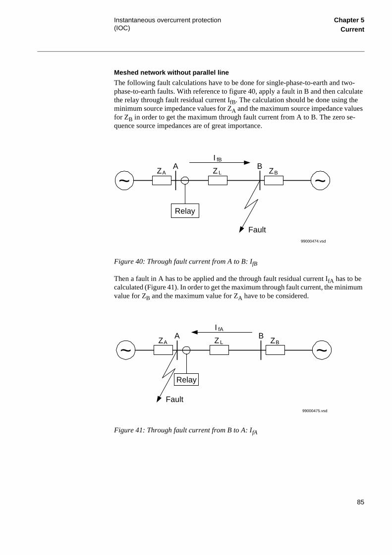
Instantaneous overcurrent protection (IOC)
Chapter 5Current
Meshed network without parallel line
The following fault calculations have to be done for single-phase-to-earth and two-phase-to-earth faults. With reference to figure 40, apply a fault in B and then calculate the relay through fault residual current IfB. The calculation should be done using the minimum source impedance values for ZA and the maximum source impedance values for ZB in order to get the maximum through fault current from A to B. The zero se-quence source impedances are of great importance.
Figure 40: Through fault current from A to B: IfB
Then a fault in A has to be applied and the through fault residual current IfA has to be calculated (Figure 41). In order to get the maximum through fault current, the minimum value for ZB and the maximum value for ZA have to be considered.
Figure 41: Through fault current from B to A: IfA
99000474.vsd
~ ~ZA ZBZ L
A B
Relay
I fB
Fault
99000475.vsd
~ ~ZA ZBZ L
A B
Relay
I fA
Fault
85
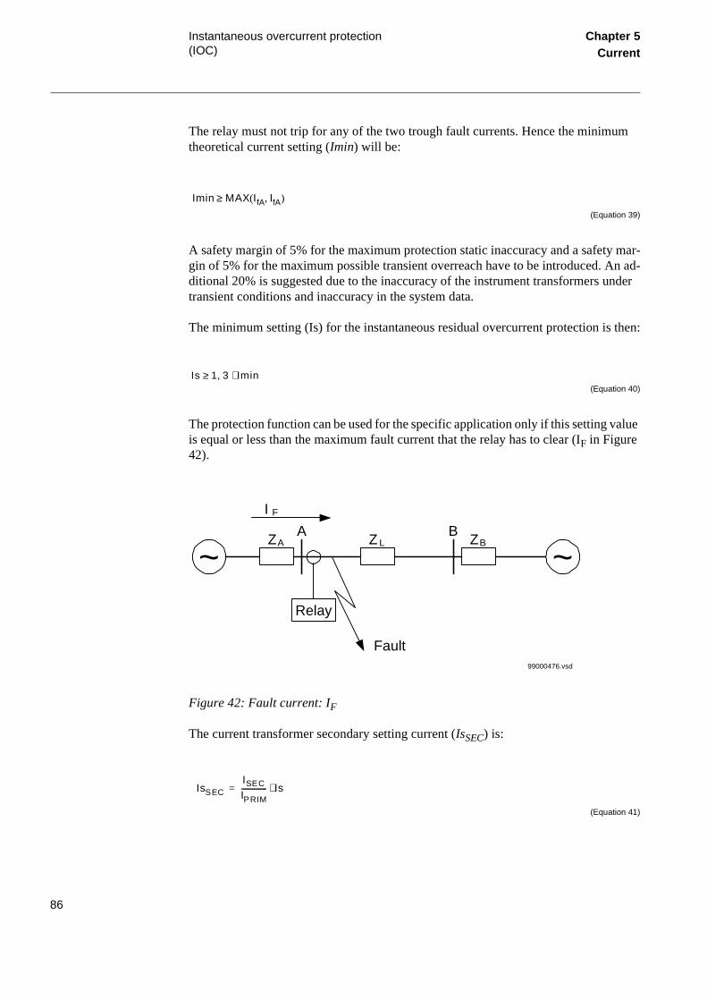
Instantaneous overcurrent protection (IOC)
Chapter 5Current
The relay must not trip for any of the two trough fault currents. Hence the minimum theoretical current setting (Imin) will be:
(Equation 39)
A safety margin of 5% for the maximum protection static inaccuracy and a safety mar-gin of 5% for the maximum possible transient overreach have to be introduced. An ad-ditional 20% is suggested due to the inaccuracy of the instrument transformers under transient conditions and inaccuracy in the system data.
The minimum setting (Is) for the instantaneous residual overcurrent protection is then:
(Equation 40)
The protection function can be used for the specific application only if this setting value is equal or less than the maximum fault current that the relay has to clear (IF in Figure 42).
Figure 42: Fault current: IF
The current transformer secondary setting current (IsSEC) is:
(Equation 41)
Imin MAX IfA IfA,( )≥
Is 1 3, Imin⋅≥
99000476.vsd
~ ~ZA ZBZ L
A B
Relay
I F
Fault
IsSECISEC
IPRIM-------------- Is⋅=
86
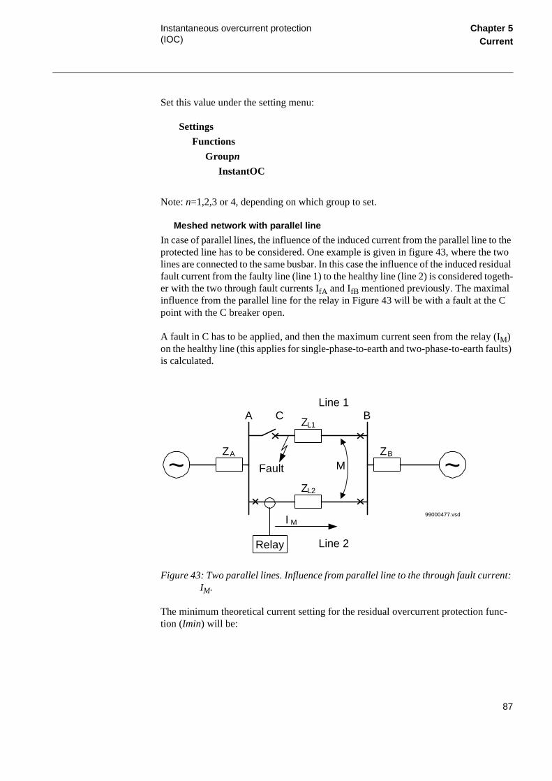
Instantaneous overcurrent protection (IOC)
Chapter 5Current
Set this value under the setting menu:
Settings
Functions
Groupn
InstantOC
Note: n=1,2,3 or 4, depending on which group to set.
Meshed network with parallel line
In case of parallel lines, the influence of the induced current from the parallel line to the protected line has to be considered. One example is given in figure 43, where the two lines are connected to the same busbar. In this case the influence of the induced residual fault current from the faulty line (line 1) to the healthy line (line 2) is considered togeth-er with the two through fault currents IfA and IfB mentioned previously. The maximal influence from the parallel line for the relay in Figure 43 will be with a fault at the C point with the C breaker open.
A fault in C has to be applied, and then the maximum current seen from the relay (IM) on the healthy line (this applies for single-phase-to-earth and two-phase-to-earth faults) is calculated.
Figure 43: Two parallel lines. Influence from parallel line to the through fault current: IM.
The minimum theoretical current setting for the residual overcurrent protection func-tion (Imin) will be:
99000477.vsd
~ ~ZA ZB
ZL1A B
I M
Fault
Relay
ZL2
M
CLine 1
Line 2
87
Instantaneous overcurrent protection (IOC)
Chapter 5Current
(Equation 42)
Where IfA and IfB have been described in the previous paragraph. Considering the safe-ty margins mentioned previously, the minimum setting (Is) for the instantaneous phase overcurrent protection is then:
(Equation 43)
The protection function can be used for the specific application only if this setting value is equal or less than the maximum residual fault current that the relay has to clear.
The current transformer secondary setting current (IsSEC) is:
(Equation 44)
Set this value under the setting menu:
Settings
Functions
Groupn
InstantOC
Note: n=1,2,3 or 4, depending on which group to set.
I m in M AX IfA I fB IM, ,( )≥
Is 1 3, Imin⋅≥
IsSECISEC
IPRIM-------------- Is⋅=
88

Time delayed overcurrent protection (TOC)
Chapter 5Current
2 Time delayed overcurrent protection (TOC)
2.1 Application
The time delayed phase overcurrent protection can be used as independent overcurrent protection, particularly for radially fed systems, or as back-up protection to the main distance or line differential protection functions. In the first case the protected zone of the time delayed overcurrent protection reaches upto the next overcurrent protection and works in its zone as back-up protection. The programmable time delay (definite time) of the function allows the time selectivity through an appropriate time grading among the overcurrent relays protecting the system.
Where the function acts as back-up for the main line protection, the trip from the over-current protection can be activated when the main protection function is blocked (e.g. by the fuse failure protection) or it can be active all the time.
In some cases, where it could be difficult to achieve a selective trip, the function can be used as a helpful overcurrent signallization for the post-fault analysis.
The time delayed residual overcurrent protection (TOC) which is an earth-fault protec-tion, serves as a built-in local back-up function to the main protection function. In most cases, it is used as a back-up for the earth-fault measuring in distance protection.
The function is intended to be used in solidly earthed systems.
The time delay makes it possible to set the relay to detect high resistance faults and still perform selective trip.
The protection, which is non-directional, is included in some of the REx 5xx terminals. Refer to the ordering information for more details.
2.2 Functionality
The current-measuring elements within one of the built-in digital signal processors con-tinuously measure the current in all three phases, and compare them with the IP> set value. A recursive Fourier filter filters the current signals, and a separate trip counter prevents high overreaching of the measuring elements. The logical value of each phase current signal on the output of the digital processor (STIL1, STIL2 and STIL3 respec-tively) is equal to 1 if the measured phase current exceeds the set value. These signals will instantaneously set their respective output starting signals (TOC--STL1, TOC--STL2, TOC--STL3), if the function is not blocked.
89

Time delayed overcurrent protection (TOC)
Chapter 5Current
, then
own
en
nt n-
ex-inal
te it
is
nly, with e
If any of the three phase currents exceeds the set value for a period longer than the set time tP, then a three phase trip is generated from the output signal TOC--TRP.
The current-measuring element within one of the built-in digital signal processors con-tinuously measures the residual current (3I0), and compares it with the IN> set value. A recursive Fourier filter filters the current signal, and a separate trip counter prevents high overreaching of the measuring element. The logical value of the signal on the out-put of the digital signal processor (TOC--STIN) is equal to 1 if the measured residual current exceeds the pre-set value. This signal will instantaneously set the output start signal (TOC--STN), unless the function is blocked (see “Design”).
The function trip signal (TOC--TRN) can be delayed 0-60 s.
If the residual current exceeds the set value for a period longer than the set valuea three phase trip is generated from the output signal TOC--TRN.
2.3 Design
The simplified logic diagram of the time delayed phase overcurrent function is shin figure 44.
The function is disabled (blocked) if:
• The terminal is in TEST mode (TEST-ACTIVE is high) and the function has beblocked from the HMI (BlockTOC=Yes).
• The input signal TOC--BLOCK is high.
The TOC--BLOCK signal is a blocking signal of the time delayed phase overcurrefunction. It prevents the activation of any trip or starting output signal. It can be conected to a binary input of the terminal in order to receive a block command fromternal devices or can be software connected to other internal functions of the termitself in order to receive a block command from internal functions. Through OR gacan be connected to both binary inputs and internal function outputs. The TOC--BLOCK signal blocks also the time delayed residual overcurrent protection, if thisinstalled in the same REx 5xx terminal.
When the function is enabled, there is still the possibility to block the output trips owithout affecting the start signals, that will always be active. This can be obtained the function input TOC--BLKTR. Similarly to the TOC--BLOCK signal, also the timdelayed residual overcurrent protection, if present in the terminal, is blocked fromTOC-BLKTR.
90
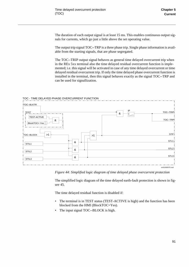
Time delayed overcurrent protection (TOC)
Chapter 5Current
een
The duration of each output signal is at least 15 ms. This enables continuous output sig-nals for currents, which go just a little above the set operating value.
The output trip signal TOC--TRP is a three phase trip. Single phase information is avail-able from the starting signals, that are phase segregated.
The TOC--TRIP output signal behaves as general time delayed overcurrent trip when in the REx 5xx terminal also the time delayed residual overcurrent function is imple-mented; i.e. this signal will be activated in case of any time delayed overcurrent or time delayed residual overcurrent trip. If only the time delayed phase overcurrent function is installed in the terminal, then this signal behaves exactly as the signal TOC--TRP and can be used for signallization.
Figure 44: Simplified logic diagram of time delayed phase overcurrent protection
The simplified logic diagram of the time delayed earth-fault protection is shown in fig-ure 45.
The time delayed residual function is disabled if:
• The terminal is in TEST status (TEST-ACTIVE is high) and the function has bblocked from the HMI (BlockTOC=Yes).
• The input signal TOC--BLOCK is high.
TOC--BLOCK
en01000075.vsd
TOC - TIME DELAYED PHASE OVERCURRENT FUNCTION
TEST-ACTIVE
&
TEST
BlockTOC= Yes
>1
STIL1
STIL2
STIL3
TOC--TRIP
TOC--TRP
&
&
TOC--BLKTR
&
t
tP&
>1 STP
STL1
STL2
STL3
91
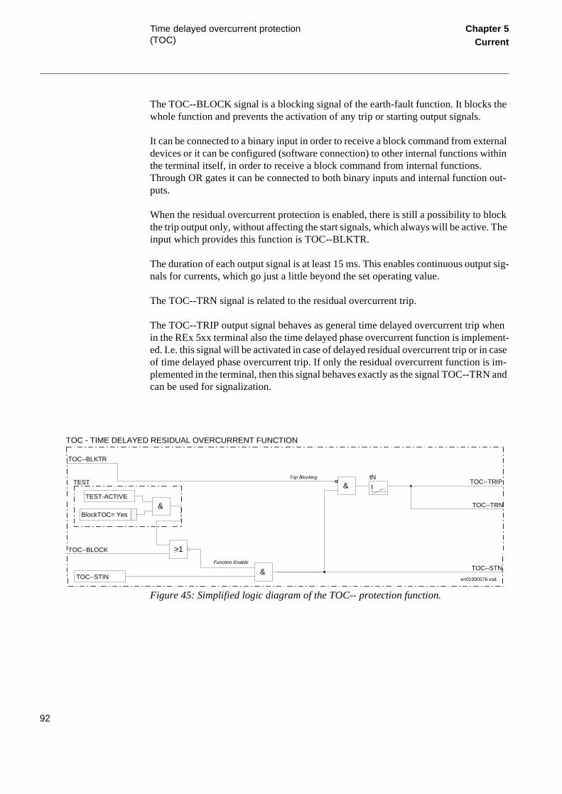
Time delayed overcurrent protection (TOC)
Chapter 5Current
The TOC--BLOCK signal is a blocking signal of the earth-fault function. It blocks the whole function and prevents the activation of any trip or starting output signals.
It can be connected to a binary input in order to receive a block command from external devices or it can be configured (software connection) to other internal functions within the terminal itself, in order to receive a block command from internal functions. Through OR gates it can be connected to both binary inputs and internal function out-puts.
When the residual overcurrent protection is enabled, there is still a possibility to block the trip output only, without affecting the start signals, which always will be active. The input which provides this function is TOC--BLKTR.
The duration of each output signal is at least 15 ms. This enables continuous output sig-nals for currents, which go just a little beyond the set operating value.
The TOC--TRN signal is related to the residual overcurrent trip.
The TOC--TRIP output signal behaves as general time delayed overcurrent trip when in the REx 5xx terminal also the time delayed phase overcurrent function is implement-ed. I.e. this signal will be activated in case of delayed residual overcurrent trip or in case of time delayed phase overcurrent trip. If only the residual overcurrent function is im-plemented in the terminal, then this signal behaves exactly as the signal TOC--TRN and can be used for signalization.
Figure 45: Simplified logic diagram of the TOC-- protection function.
TOC--BLOCK
en01000076.vsd
TOC - TIME DELAYED RESIDUAL OVERCURRENT FUNCTION
TEST-ACTIVE
&
TEST
BlockTOC= Yes
>1
TOC--STIN
TOC--TRIP
TOC--TRN
&
TOC--BLKTR
t
tN&
TOC--STNFunction Enable
Trip Blocking
92
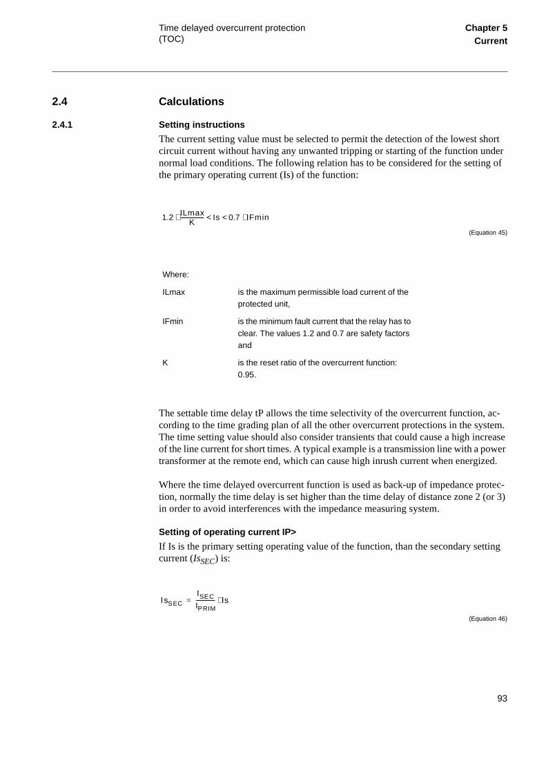
Time delayed overcurrent protection (TOC)
Chapter 5Current
2.4 Calculations
2.4.1 Setting instructions
The current setting value must be selected to permit the detection of the lowest short circuit current without having any unwanted tripping or starting of the function under normal load conditions. The following relation has to be considered for the setting of the primary operating current (Is) of the function:
(Equation 45)
The settable time delay tP allows the time selectivity of the overcurrent function, ac-cording to the time grading plan of all the other overcurrent protections in the system. The time setting value should also consider transients that could cause a high increase of the line current for short times. A typical example is a transmission line with a power transformer at the remote end, which can cause high inrush current when energized.
Where the time delayed overcurrent function is used as back-up of impedance protec-tion, normally the time delay is set higher than the time delay of distance zone 2 (or 3) in order to avoid interferences with the impedance measuring system.
Setting of operating current IP>
If Is is the primary setting operating value of the function, than the secondary setting current (IsSEC) is:
(Equation 46)
Where:
ILmax is the maximum permissible load current of the protected unit,
IFmin is the minimum fault current that the relay has to
clear. The values 1.2 and 0.7 are safety factors and
K is the reset ratio of the overcurrent function:
0.95.
1.2 ILmaxK
-----------------⋅ Is 0.7 IFmin⋅< <
IsSEC
ISEC
IPRIM-------------- Is⋅=
93

Time delayed overcurrent protection (TOC)
Chapter 5Current
The relay setting value IP> is given in percentage of the secondary base current value, I1b, associated to the current transformer input I1. The value for IP> is given from this formula:
(Equation 47)
This is the value that has to be set in the terminal.
Set this value under the setting menu:
Settings
Functions
Group n
TimeDelayOC
On the value IP>.
Setting of time delay tP
Set the time delay of the function, tP, under the setting menu:
Settings
Functions
Group n
TimeDelayOC
on the value tP.
Where:
ISEC is the secondary rated current of the main CT
and
IPRIM is the primary rated current of the main CT.
IP>IsSEC
I1b--------------- 100⋅=
94
Time delayed overcurrent protection (TOC)
Chapter 5Current
2.4.2 Setting instructions
The residual overcurrent protection is very sensitive to the change of zero source im-pedance. Since it must operate only in a selective way, it is necessary to check all sys-tem and transient conditions that can cause unwanted operation.
The settings should be chosen in such a way that it can detect high resistance faults on the protected line and still be selective to other residual time delayed protections in both forward and reverse directions. The time setting value should also consider transients that can cause a high increase of the residual line current for short times.
A typical example is a transmission line with a power transformer at the remote end, which can cause high inrush current when being energised.
In well transposed system, the false earth-fault current is normally lower than 5% of the line current. For non transposed lines a considerably higher false residual current may be found.
In case of extremely short or not fully transposed parallel lines, the false residual current must be measured or calculated when maximum sensitivity is desired. Generally, 80 A is recommended as a minimum primary operation value for the residual overcurrent protection.
General criteria for the primary current setting value of the time delayed residual over-current protection is given in the formula below:
(Equation 48)
Where:
IRmax is the maximum permissive residual current flowing in the protection unit during normal service conditions and
IFmin is the minimum residual fault current that the relay has to clear.
1.3 and
are safety factor values. 0.7
1.3 IRmax⋅ Is 0.7 IFmin⋅< <
95
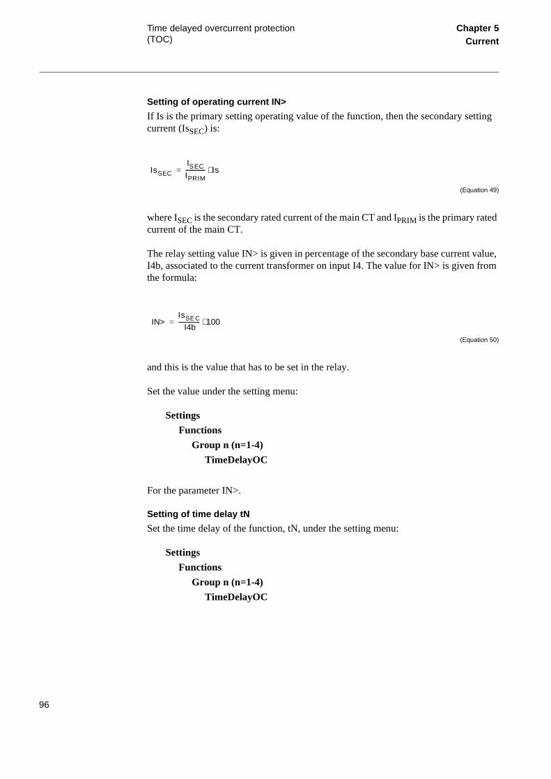
Time delayed overcurrent protection (TOC)
Chapter 5Current
Setting of operating current IN>
If Is is the primary setting operating value of the function, then the secondary setting current (IsSEC) is:
(Equation 49)
where ISEC is the secondary rated current of the main CT and IPRIM is the primary rated current of the main CT.
The relay setting value IN> is given in percentage of the secondary base current value, I4b, associated to the current transformer on input I4. The value for IN> is given from the formula:
(Equation 50)
and this is the value that has to be set in the relay.
Set the value under the setting menu:
Settings
Functions
Group n (n=1-4)
TimeDelayOC
For the parameter IN>.
Setting of time delay tN
Set the time delay of the function, tN, under the setting menu:
Settings
Functions
Group n (n=1-4)
TimeDelayOC
IsSEC
ISEC
IPRIM-------------- Is⋅=
IN>IsSE C
I4b--------------- 100⋅=
96
Two step time delayed phase overcurrent protection (TOC2)
Chapter 5Current
3 Two step time delayed phase overcurrent protection (TOC2)
3.1 Application
The time delayed phase overcurrent function is to be used as short-circuit protection in three phase networks operating at 50 or 60 Hz. It is intended to be used either as primary protection or back-up protection for differential functions or impedance measuring functions.
In radial networks it is often sufficient to use phase overcurrent relays as short circuit protection for lines, transformers and other equipment. The current time characteristic should be chosen according to common practice in the network. It is strongly recom-mended to use the same current time characteristic for all overcurrent relays in the net-work. This includes overcurrent protection for transformers and other equipment.
There is a possibility to use phase overcurrent protection in meshed systems as short cir-cuit protection. It must however be realized that the setting of a phase overcurrent pro-tection system in meshed networks, can be very complicated and a large number of fault current calculations are needed. There are situations where there is no possibility to have selectivity with a protection system based on overcurrent relays in a meshed sys-tem.
The measuring function contains one current measuring element for each phase, each of them with a low set and a high set measuring step. The low set step can have either definite time or inverse time characteristic. The characteristics available are extremely inverse, very inverse, normal inverse or RI inverse. The high set step has definite time delay.
The settings are common for all phases but both the low and high set step can be set On/Off individually and also have individual inputs for blocking.
3.2 Functionality
The time delayed overcurrent protection is used as short-circuit protection in power sys-tems, either as the primary protection or as a back-up function for selective differential protection or impedance measuring protection.The protection function comprises of measuring circuits for the three phase currents, each with a low and high current setting. The low current setting has definite or inverse time-delay while the high current setting has only definite time-delay. The measuring circuits share common settings for all phases, however, both the low and high current settings can be blocked or enabled in-dependent of the other setting.
97

Two step time delayed phase overcurrent protection (TOC2)
Chapter 5Current
Figure 46 shows a simplified logic diagram for the two step phase overcurrent protec-tion.
Figure 46: Two step time delayed phase overcurrent protection, simplified logic dia-gram
3.3 Calculations
3.3.1 Setting instructions
The phase overcurrent protection can be used in different applications. In most applica-tions it is required that all short circuits within a protected zone shall be detected and cleared and the fault clearance shall be selective. As the protection can be used in sev-eral applications only some examples are discussed.
&
Characteristic = Def
Characteristic = NI/VI/EI/RI
& ≥1 t
tLow
& TOC2-TRLS
I>Inv
IL1-3I>Low
t
tMinInv
& TOC2-STLS
& t
tHigh& TOC2-TRHS
TOC2-BLOCK
TOC2-BLKTRLS
TOC2-BLKTRHS
t50 ms
I>High
&
&
en01000090.vsd
&
98
Two step time delayed phase overcurrent protection (TOC2)
Chapter 5Current
Line protection in radial network
The phase overcurrent protection is suitable to use in radial systems without any fault current infeed from the radial feeders.
The pick up current setting (inverse time relays) or the lowest current step (constant time relays) must be given a current setting so that the highest possible load current does not cause relay operation. Here consideration also has to be taken to the relay reset cur-rent, so that a short peak of overcurrent does not cause operation of the relay even when the overcurrent has ceased.
The lowest setting value can be written:
(Equation 51)
The maximum load current on the line has to be estimated. From operation statistics the load current up to the present situation can be found. Also emergency situations must be considered. The current setting must be valid also for some years ahead.
There is also a demand that all faults, within the zone that the protection shall cover, must be detected by the phase overcurrent relay. The minimum fault current Iscmin, to be detected by the relay, must be calculated. Taking this value as a base, the highest pick up current setting can be written:
(Equation 52)
Where:
1.2 is a safety factor due to load estimation uncertainty etc.,
k the resetting ratio of the relay (about 0.95) and
Imax the maximum load current.
Ipu 1.2Imax
k-----------⋅≥
Ipu 0.7≤ Iscmin⋅
99
Two step time delayed phase overcurrent protection (TOC2)
Chapter 5Current
As a summary the pick up current shall be chosen within the interval:
(Equation 53)
The high current function of the overcurrent relay, which only has a short or no delay of the operation, must be given a current setting so that the relay is selective to other relays in the power system. It is desirable to have a rapid tripping of faults within as large portion as possible of the part of the power system to be protected by the relay (primary protected zone). A fault current calculation gives the largest current of faults, Iscmax, at the most remote part of the primary protected zone. Considerations have to be made to the risk of transient overreach, due to a possible DC component of the short circuit current. The lowest current setting of the most rapid stage, of the phase overcur-rent relay, can be written:
(Equation 54)
Where:
0.7 is a safety factor, due to calculation uncertainty and
Iscmin the smallest fault current to be detected by the overcurrent protection.
Where:
1.2 is a safety factor, due to calculation uncertainty
kt is a factor that takes care of the transient overreach due to the DC component of the fault current. kt is less than 1.05 if the power system time constant is less than 100 ms.
Iscmax is the largest fault current at a fault at the most remote point of the primary pro-tection zone.
1.2Imax
k-----------⋅ Ipu 0.7≤ ≤ Iscmin⋅
Ihigh 1.2≥ kt Iscmax⋅ ⋅
100
Two step time delayed phase overcurrent protection (TOC2)
Chapter 5Current
The operate times of the phase-overcurrent protection have to be chosen so that the fault time is so short that equipment will not be damaged due to thermal overload, at the same time selectivity is assured. For overcurrent protection, in a radial fed network, the time setting can be chosen in a graphical way. This is mostly used in the case of inverse time overcurrent protections.
Line protection in meshed network
The current setting can be made in the same way as for radial networks.
If inverse time characteristics are used with equal current and time setting for all phase current protections in the system the selectivity is assured as long as there are more than two bays carrying fault current to each substation. Sometimes this is however impossi-ble due to the fault current distribution between the different lines.
If definite time characteristic is used the co-ordination between the different phase over-current line protections is done by means of current setting.
As the phase overcurrent protection often is used as a back-up protection of lines, where a distance protection is the main protection, relatively long operation times are accept-able for the phase overcurrent protection.
Setting characteristics
Following formulas are valid for the inverse time characteristic:
Table 6: Formulas for the inverse time characteristic
Characteristic: Time delay(s):
Normal inverse(Equation 55)
Very inverse(Equation 56)
Extremely inverse(Equation 57)
RI inverse(Equation 58)
t0 14,
I0 02,
1–--------------------- k⋅=
t 13 5,I 1–------------- k⋅=
t 80
I2 1–------------- k⋅=
t 10 339, 0 236,( ) I⁄⟨ ⟩–------------------------------------------------------ k⋅=
101

Two step time delayed phase overcurrent protection (TOC2)
Chapter 5Current
The decisive factors for the setting of inverse time characteristic are the allowable time for disconnection of fault at minimum fault current that the function shall operate for together with selectivity at maximum fault current.
The settings are given in Setting table. Setting of parameters are found in the menu un-der:
Settings
Functions
Group n (n=1-4)
InvTDelay
Where:
I denotes (measured current)/ I>Inv and
k is a time multiplier with setting range 0,05 - 1,10.
102
Definite and inverse time-delayed residual overcurrent protection (TEF)
Chapter 5Current
4 Definite and inverse time-delayed residual overcurrent protection (TEF)
4.1 Application
This earth-fault overcurrent protection is intended for solidly earthed networks.
Earth-fault overcurrent protection
In case of single-phase earth-faults, the primary fault resistance varies with the network conditions, the type of fault and location of the fault. In many cases, the fault resistance is much higher than the resistance that can be covered by an impedance-measuring dis-tance protections. This can be the case with a phase to earth fault to a tower with large tower footing resistance.
Earth-faults with high fault resistances can be detected by measuring the residual cur-rent (3I0).
The inrush current can cause unwanted tripping of the earth-fault overcurrent relay when energizing a directly earthed power transformer. The earth-fault overcurrent pro-tection is therefore provided with second harmonic restraint, which blocks the operation if the residual current (3I0) contains 20% or more of the second harmonic component.
In some cases, it is possible to improve the selectivity by adding a settable minimum operate current (IMin) and a minimum operate time (tMin) to the inverse characteristic. These functions are included in the earth-fault protection modules.
To minimize the operate time, in case of closing the circuit breaker to a fault, the resid-ual overcurrent protection module is provided with a switch-onto-fault logic, which can be activated at breaker closure. The tripping time will temporarily be reduced to 300 ms.
In order to achieve the most sensitive earth fault protection the non-directional function can be used. As the residual current is normally very small during normal operation the setting value can be set very low. In case of small residual currents, due to high resis-tance phase to earth faults or serial faults, the residual voltage in the system can be very low. A serial fault can be caused by broken phase conductor(s) with no contact to earth, or pole discrepancy in a circuit breaker or a disconnector. The most common type of serial fault is pole discrepancy at breaker maneuvers.
As the residual voltage is often very small at high resistance earth faults and serial faults, any directional element can not be used.
103
Definite and inverse time-delayed residual overcurrent protection (TEF)
Chapter 5Current
The function can have different types of time-current characteristics; definite time delay or different types of inverse time delay. By using the inverse time delay characteristics some degree of selectivity between non-directional residual protection can be achieved.
4.2 Functionality
4.2.1 Theory of operation
Directional earth-fault overcurrent protection
This protection measures the residual current (3I0) and the residual voltage (3U0). Fig-ure 47 shows the current measuring, time delay and logic circuits (both with and with-out directional check) of this protection function.
104
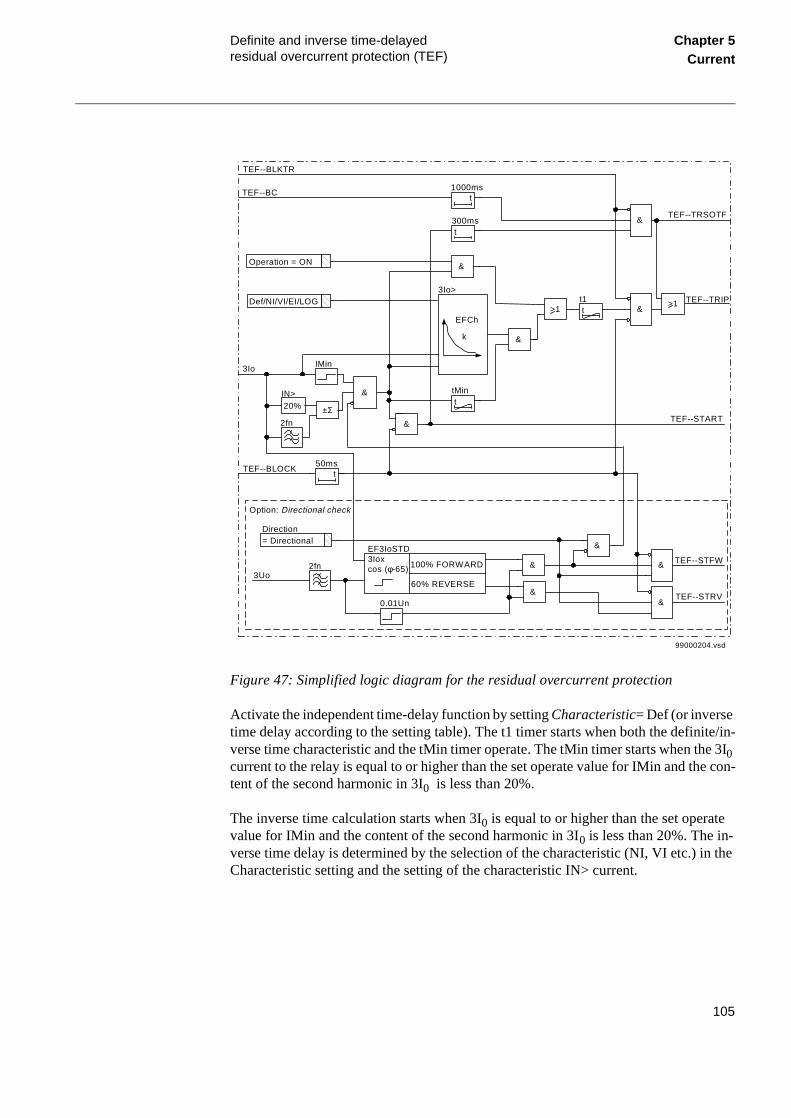
Definite and inverse time-delayed residual overcurrent protection (TEF)
Chapter 5Current
Figure 47: Simplified logic diagram for the residual overcurrent protection
Activate the independent time-delay function by setting Characteristic= Def (or inverse time delay according to the setting table). The t1 timer starts when both the definite/in-verse time characteristic and the tMin timer operate. The tMin timer starts when the 3I0 current to the relay is equal to or higher than the set operate value for IMin and the con-tent of the second harmonic in 3I0 is less than 20%.
The inverse time calculation starts when 3I0 is equal to or higher than the set operate value for IMin and the content of the second harmonic in 3I0 is less than 20%. The in-verse time delay is determined by the selection of the characteristic (NI, VI etc.) in the Characteristic setting and the setting of the characteristic IN> current.
99000204.vsd
Operation = ON
Def/NI/VI/EI/LOG
&
&
>1
EFCh
k
IN>
±Σ
300mst
1000mst
3Io>
ttMin
&
tt1
&
IMin
20%
50mst
TEF--TRIP
= Directional
100% FORWARD
60% REVERSE
3Ioxcos (φ-65)
EF3IoSTD
0.01Un
2fn
2fn
Direction
Option: Directional check
3Uo
TEF--BLOCK
&
&
&
&
&
TEF--TRSOTF
TEF--STFW
TEF--STRV
TEF--START
TEF--BC
TEF--BLKTR
3Io
>1
&
&
105

Definite and inverse time-delayed residual overcurrent protection (TEF)
Chapter 5Current
The t1 timer is normally set to zero. Use it to add a constant time to the inverse time delay. Figure 48 shows the effect of the IMin and tMin settings on the inverse charac-teristic.
Figure 48: Normal inverse and logarithmic inverse time characteristics.
The switch-onto-fault function is used to minimise the operate time in case of pole dis-crepancy at breaker closing and in cased of closing on to a fault. The function is released by activating the TEF--BC binary input. The function is activated for 1 second after the reset of the TEF--BC binary input.
The function is blocked by activating the TEF--BLOCK binary input.
Activating the TEF--BLKTR blocks the definite/inverse delay trip outputs TEF--TRIP and the switch-on-to-fault trip TEF-TRSOTF.
4.3 Calculations
4.3.1 Setting instructions
To detect high resistive earth-faults, a low operate current is required. On the other hand, a low setting increases the risk for unwanted operation due to imbalance in the network and the current transformer circuits. Set the minimum operate current (IN> *IMin) of the earth-fault overcurrent protection higher than the maximum false earth-fault current. If the directional function is chosen, set the start level of the directional function (IN> Dir) higher than the maximum false earth-fault current.
1
2
3
4
5
1 2 3 5 7 10 20 30 50
LogaritmicInverse
NormalInverse(k=0,4)
x IN>
t (s)
99000105.vsd
tMIN
IMIN
106
Definite and inverse time-delayed residual overcurrent protection (TEF)
Chapter 5Current
The imbalance in the network that causes false earth-fault currents is caused mainly by untransposed or not fully transposed parallel lines with strong zero-sequence mutual coupling. There might also be high imbalance currents for non-transposed single circuit lines if the zero sequence source impedance is low at both line ends. This false earth-fault current is directly proportional to the load current.
In a well-transposed system, the false earth-fault current is normally lower than 5% of the line current.
In case of not fully transposed parallel lines, measure or calculate the false earth-fault current at maximum load.
The choice of time delay characteristics - definite time, normal inverse, very inverse, extremely inverse or logarithmic inverse - depends on the network. To achieve opti-mum selectivity, use the same type of characteristic for all earth-fault overcurrent pro-tections in the network. This means that in networks already equipped with earth-fault overcurrent relays, the best selectivity is normally achieved by using the same type of characteristic as in the existing relays.
The following formulas for the operate time (in seconds) apply to the characteristic used within the REx 5xx terminal with line protection, see table 7.
Table 7: Operate time formulas
Characteristics Operate time (s)
Normal inverse(Equation 59)
Very inverse(Equation 60)
Extremely inverse(Equation 61)
Logarithmic inverse(Equation 62)
Where:
I is a multiple of set current 3I0>
k is a time multiplying factor, settable in the range of 0.05 to 1.10
t 0.14
I0.02 1–-------------------- k⋅=
t 13.5I 1–----------- k⋅=
t 80
I2 1–------------- k⋅=
t 5.8 1.35 Iln⋅( )–=
107
Definite and inverse time-delayed residual overcurrent protection (TEF)
Chapter 5Current
All inverse time characteristic settings are a compromise between short fault clearing time and selective operation in a large current range. The main determining factors are the maximum allowed fault-clearing time at the maximum fault resistance to be covered and the selectivity at maximum fault current.
Set the minimum operate current (IMin) of the earth-fault overcurrent protection to one to four times the set characteristic quantity (IN>) of the inverse time delay. So an in-verse characteristic with a low set IN> set to get a short operate time at minimum fault current can be combined with a higher set IMin minimum operate current, to avoid un-wanted operation due to false earth-fault currents.
Set the minimum operate time independent of the inverse time characteristic. Normally, set this time longer than the time delay of distance zone 2 in REx 5xx to avoid interfer-ence with the impedance measuring system in case of earth-faults with moderate fault resistance within zone 2.
When a solidly earthed, power transformer is energized, an inrush current normally flows in the neutral-to-earth connection of the transformer. This current is divided among other earthed transformers and lines connected to the same bus, inversely pro-portional to their zero-sequence impedance. The amplitude and time duration of this current can be sufficiently large to cause the unwanted operation of a sensitive earth-fault overcurrent protection.
The earth-fault overcurrent protection has a built-in second harmonic current stabiliza-tion, which prevents unwanted operation if the inrush current has a second harmonic content of 20% or more. This is normally the case. On rare occasions, it may be neces-sary to increase the setting of the operate value for the residual earth-fault overcurrent protection to avoid unwanted operation due to transformer inrush current.
When single-phase auto-reclosing is used, the minimum time of the inverse time de-layed residual overcurrent protection (tMin) should be set to be longer than the time from the occurrence of the fault to the reclosing of the breaker at both line terminals. An alternative method is to block the earth fault protection by the autorecloser during the dead time. This avoids unwanted three-phase tripping during a single-phase auto-reclosing cycle controlled by the distance protection.
The polarizing voltage for directional earth-fault overcurrent protection is normally ob-tained from the broken delta windings of instrument voltage transformers or by internal calculation. The voltage contains a certain amount of harmonics, especially when the protection is connected to CVTs.
Due to the bandpass filtering a polarizing voltage down to 1 percent of the rated voltage will provide correct directional functionality. This is also valid when the protection is connected to CVTs.
108
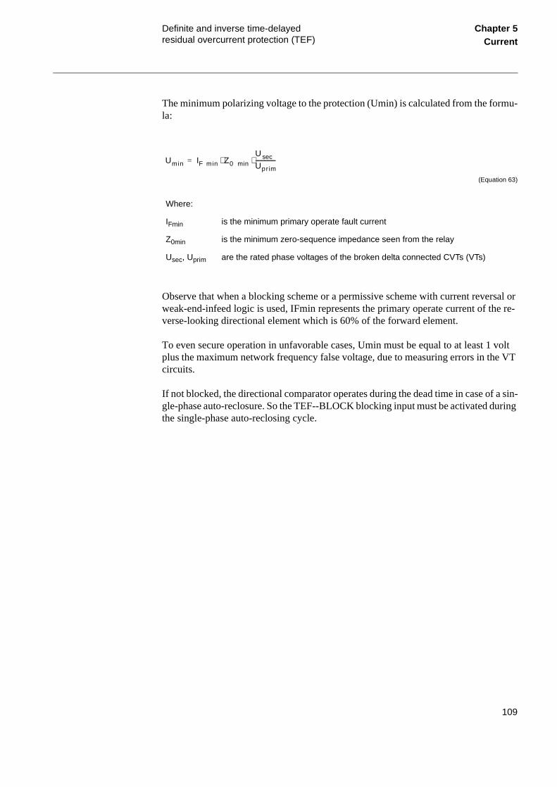
Definite and inverse time-delayed residual overcurrent protection (TEF)
Chapter 5Current
The minimum polarizing voltage to the protection (Umin) is calculated from the formu-la:
(Equation 63)
Observe that when a blocking scheme or a permissive scheme with current reversal or weak-end-infeed logic is used, IFmin represents the primary operate current of the re-verse-looking directional element which is 60% of the forward element.
To even secure operation in unfavorable cases, Umin must be equal to at least 1 volt plus the maximum network frequency false voltage, due to measuring errors in the VT circuits.
If not blocked, the directional comparator operates during the dead time in case of a sin-gle-phase auto-reclosure. So the TEF--BLOCK blocking input must be activated during the single-phase auto-reclosing cycle.
Where:
IFmin is the minimum primary operate fault current
Z0min is the minimum zero-sequence impedance seen from the relay
Usec, Uprim are the rated phase voltages of the broken delta connected CVTs (VTs)
Umin IF min Z0 min
U sec
Uprim--------------⋅ ⋅=
109

Thermal overload protection (THOL) Chapter 5Current
ction
per-IP
ive as
5 Thermal overload protection (THOL)
5.1 Application
When the load currents exceed the permitted continuous current there is a risk that the conductor or the insulation will be subject to permanent damage due to overheating. Even moderate overloads under long time give appreciable temperature increase. For example, a current of 1.2 times rated load current gives a temperature rise of 1.2 x 1.2 = 1.44 times rated value.
The temperature rise as a function of time for a fixed load is determined by the so called thermal time constant τ of the element.Moderate overloads are normally not detected by current or impedance measuring relays. A current thermal overload protection can prevent damage caused by excessive temperature increase due to moderate or heavy current overloads.
Electrical cables which can be loaded up to the permissible load current should be pro-vided with thermal protection. For cables surrounded by air, the thermal time constant τ can vary from some few minutes for 10 kV cables with small cross-sectional area to more than one hour for high voltage cables with large cross-sectional area. The shorter time constant valid for cables in air is decisive if some part of the cable is surrounded by air.
For overhead lines and cables placed in the air, the ambient temperature will normally vary considerably. Since the temperature of the element is the sum of the ambient tem-perature and the temperature rise, the thermal protection for heavily loaded lines should be provided with compensation for the ambient temperature.The heating effect of radi-ant power from the sun can also be appreciable in some areas.
5.2 Functionality
The function includes a memory that is continuously updated with the heat content of the line based on the RMS value of the line current and the ambient temperature. The current used in the function is the phase current having the highest RMS value out of the three phase currents. The function has two settable operating levels for temperature, one intended for alarm and one intended for tripping. For the tripping function a reset hysteresis is included that can be set between 5 and 30°C while for the alarm funit is fixed at 5°C hysteresis.
For the alarm there is an output denoted ALARM which is active as long as the temature is above alarm level. For the tripping there are two outputs, one denoted TRwhich gives only a 50 ms pulse at operation and one denoted START which is actlong as the temperature is above tripping level.
110
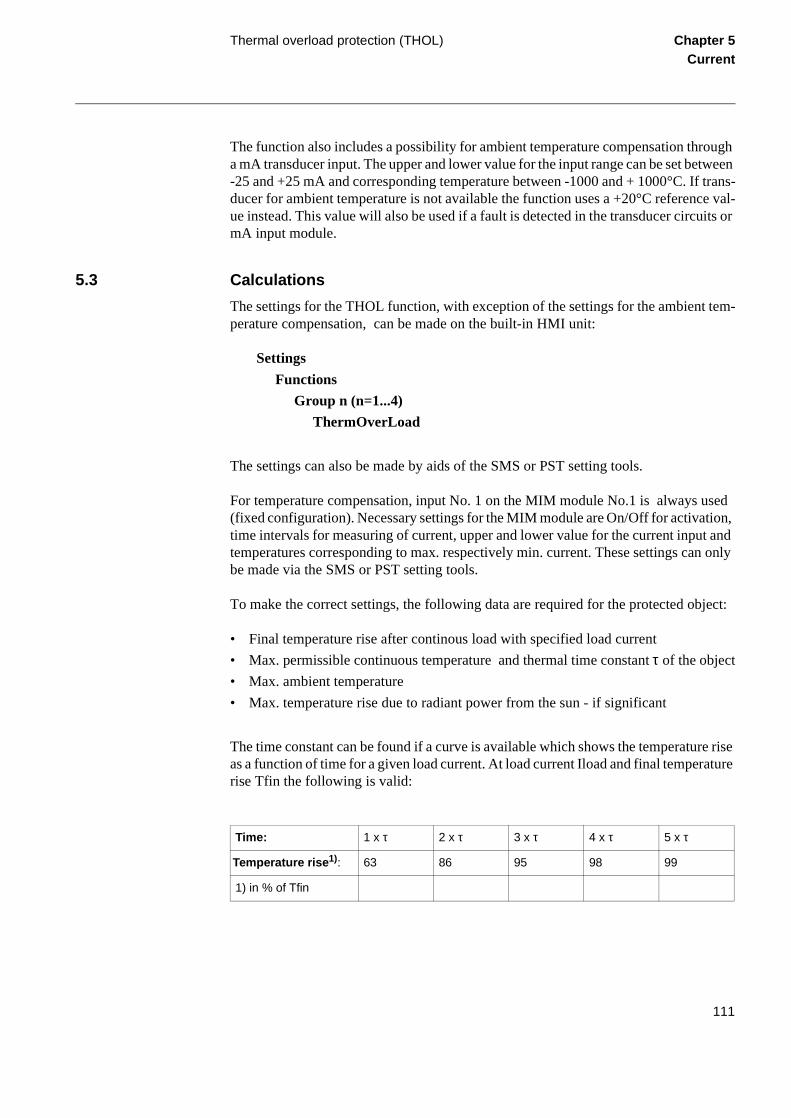
Thermal overload protection (THOL) Chapter 5Current
trans-e val-its or
tem-
sed on, and only
ject:
e rise ture
The function also includes a possibility for ambient temperature compensation through a mA transducer input. The upper and lower value for the input range can be set between -25 and +25 mA and corresponding temperature between -1000 and + 1000°C. Ifducer for ambient temperature is not available the function uses a +20°C referencue instead. This value will also be used if a fault is detected in the transducer circumA input module.
5.3 Calculations
The settings for the THOL function, with exception of the settings for the ambient perature compensation, can be made on the built-in HMI unit:
Settings
Functions
Group n (n=1...4)
ThermOverLoad
The settings can also be made by aids of the SMS or PST setting tools.
For temperature compensation, input No. 1 on the MIM module No.1 is always u(fixed configuration). Necessary settings for the MIM module are On/Off for activatitime intervals for measuring of current, upper and lower value for the current inputtemperatures corresponding to max. respectively min. current. These settings canbe made via the SMS or PST setting tools.
To make the correct settings, the following data are required for the protected ob
• Final temperature rise after continous load with specified load current
• Max. permissible continuous temperature and thermal time constant τ of the object
• Max. ambient temperature
• Max. temperature rise due to radiant power from the sun - if significant
The time constant can be found if a curve is available which shows the temperaturas a function of time for a given load current. At load current Iload and final temperarise Tfin the following is valid:
Time: 1 x τ 2 x τ 3 x τ 4 x τ 5 x τ
Temperature rise1): 63 86 95 98 99
1) in % of Tfin
111
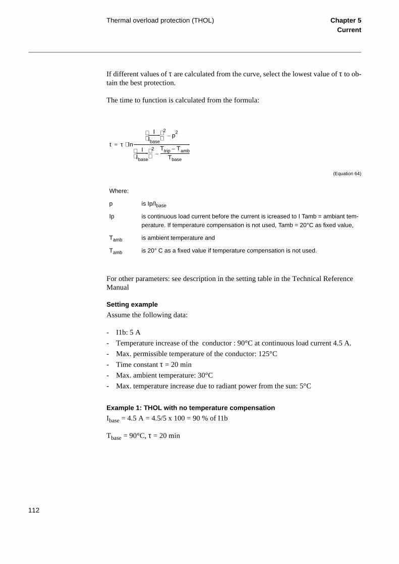
Thermal overload protection (THOL) Chapter 5Current
A.
If different values of τ are calculated from the curve, select the lowest value of τ to ob-tain the best protection.
The time to function is calculated from the formula:
(Equation 64)
For other parameters: see description in the setting table in the Technical Reference Manual
Setting example
Assume the following data:
- I1b: 5 A
- Temperature increase of the conductor : 90°C at continuous load current 4.5
- Max. permissible temperature of the conductor: 125°C
- Time constant τ = 20 min
- Max. ambient temperature: 30°C
- Max. temperature increase due to radiant power from the sun: 5°C
Example 1: THOL with no temperature compensation
Ibase = 4.5 A = 4.5/5 x 100 = 90 % of I1b
Tbase = 90°C, τ = 20 min
Where:
p is Ip/Ibase
Ip is continuous load current before the current is icreased to I Tamb = ambiant tem-
perature. If temperature compensation is not used, Tamb = 20°C as fixed value,
Tamb is ambient temperature and
Tamb is 20° C as a fixed value if temperature compensation is not used.
t τ In
IIbase------------
2p
2–
IIbase------------
2 Ttrip Tamb–
Tbase-----------------------------–
--------------------------------------------------------⋅=
112
Thermal overload protection (THOL) Chapter 5Current
of the er is
s con- 30 +
at
5°C ce the
The thermal function assumes 20°C ambient temperature as a fixed value insteadactual value 30°C. Also, the 5°C temperature increase due to the sun radiant pownot included in the calculated temperature increase. Hence, the function calculatetinous conductor temperature 20 + 90 = 110°C at 4.5 A whereas the max. value is90 +5 = 125°C. Hence the setting should be TTrip = 125 - (125 - 110 ) = 110°C.
Example 2: THOL with temperature compensation
Assume temperature measuring elements with output 4 mA at -20°C and 20 mA 100°C. Settings of Ibase, Tbase and τ same as above
.MI11-I-Max= 20.00mA MI11-I-MaxValue = +100°C
CMI11-I-Min= 4.00mA MI11-I-MinValue = -20°C
The influence of the ambient temperature is included in the calculated values. Thetemperature increase due to the sun radiant power, however, is not included. Hensetting should be Ttrip = 125 - 5 = 120°C.
113

Breaker failure protection (BFP) Chapter 5Current
6 Breaker failure protection (BFP)
6.1 Application
This function issues a back-up trip command to trip adjacent circuit breakers in case of a tripping failure of the circuit breaker (CB), and clears the fault as requested by the ob-ject protection.
The breaker-failure function is started by a protection trip command, from the line and busbar protection through the breaker-related trip relays. The start can be single-phase or three-phase. Correct fault current clearing or failure is detected by a current check in each phase. The current level can be set at 0,05 to 2 times the rated current.
Retrip of the faulty CB can be done with or without current check. A delay, 0-60 s, can be set for the retrip.
The use of retrip, limits the impact on the power system if the breaker-failure protection function (BFP) is started by mistake during testing or other maintenance work.
A second time step is used for the back-up trip command. It should be connected to trip the adjacent breakers, to clear the busbar section and intertrip the remote end, if so re-quired. The time setting range is 0-60 s.
By using separate timers for each phase, correct operation at evolving faults is ensured.
The timer setting should be selected with a certain margin to allow variation in the nor-mal fault clearing time. The properties of the BFP function allow the use of a small mar-gin.
114

Breaker failure protection (BFP) Chapter 5Current
k-up
back-
Figure 49: Simplified logic diagram - Start and trip functions
The application functions of the protection are:
• Individual phase-current detection
• Two time steps, one for retrip of the related circuit breaker and one for the bactrip of the adjacent circuit breakers
• Selection of current controlled or unconditional retrip
• Phase separated timers gives correct operation at an evolving fault
• Accurate timers and current elements reset in 10 ms, allowing the use of shortup trip time
IL1
BFP-STL1
RTL1
IL2
&>1L1
BUTL1STARTL1
BUTL2STARTL2
RTL2L2
tp
>1
tp
&>1 >1
L3RTL3
BUTL3STARTL3
tp
&>1
TTRIP
BFP-STL2BFP-START
IL3
BFP-STL3
BFP-BLOCK
BFP-TRRETL1
BFP-TRRET
BFP-TRRETL2
BFP-TRBU
BFP-TRRETL3
99000046.vsd
115

Breaker failure protection (BFP) Chapter 5Current
Figure 50: Time sequence
6.2 Functionality
The breaker-failure protection starts on a single-phase or three-phase condition, either from an external protection, or internally from a protection trip signal in the terminal.
The breaker receiving the original protection trip command can be retripped from the BFP. The retrip can be controlled by a current check, or carried out as a direct retrip without any current check. The direct retrip can be used, because the breaker-to-trip has already received a tripping command, and the direct retrip does not cause any unselec-tive tripping
The use of retrip, limits the extent of unwanted power disconnection in case of an acci-dental start of the BFP at work in the initiating circuits, with the primary circuit in ser-vice and the load above the set current level.
The back-up trip is sent to the adjacent circuit breakers in order to clear the fault and disconnect the failing circuit breaker.
Relaytime
30 ms
CB Opening time
40 ms
NormalCB OpeningStart BFP
Marginal
20 ms
<10 ms
BFPTime CB Opening time
40 ms
Retriporiginal CB
General tripadjacent CB
110 ms 150 ms
Marginal
20 ms BFPtime
<10 ms
99000047.vsd
116

Breaker failure protection (BFP) Chapter 5Current
ura- the
Figure 51: Logic diagram of breaker-failure protection, phase L1
Input and output signals
Figure 52: Input and output signals
The connectable inputs are connectable by configuration to the binary inputs of the ter-minal or to other internal functions’ outputs. The outputs are connectable by configtion to the binary output relays. “Connectables” and “outputs” can be connected tofree-logic functions of the unit, OR gates, and in that way add connection links
&
&
RMSASD
t
t
t
t
BFP-STL1
IL1
t2
t1
t1
RET1
RET0RET2
BFP-BUTL1
BFP-RTL1
L1
RET0 : No retripRET1 : Retrip with current checkRET2 : Unconditional retrip
>1>1
>1>1
External start
TRIPL1TRIPL2TRIPL3TPTRIP
STL1STL2STL3STARTBLOCK TRRETL1
TRRETL2TRRETL3
TRRETTRBU
Trip Logic Breaker-failureprotection
99000049.vsd
117
Breaker failure protection (BFP) Chapter 5Current
e-
nt due t rep-
t base
ax-
n-ault sta-
ever
e cur-o rap-sed. and et cur-
fil-g oc-
l, re-has
Start functions
The breaker-failure protection can be started either internally or externally. The start pulse is sealed-in as long as the current exceeds the preset current level, to prevent a restart of the BFP timers in case of a chattering starting contact. The preset current level may be set to (0.05 - 2.0) · Ir where Ir is 1 or 5 A.
Measuring principles
The current is filtered through a specially designed high-pass filter to obtain the rquired suppression of the dc components.
High-pass filtering is performed basically for two reasons, i.e. to remove the:
• dc component caused by saturated current transformers with a decaying curreto de-energizing of the secondary circuit. This is done to achieve a more correcresentation of the real current in the line.
• dc component that is a part of the fault current. This is done to achieve a correcfor both ASD and RMS calculations.
The frequency limit of the filter is very close to the service frequency, to obtain a mimum suppression of the above dc components.
The intention of the adaptive signal detection (ASD) concept is to achieve indepedence from the absolute filtering requirement, when dealing with extremely high fcurrents in combination with low preset values. This is obtained by creating a newbilizing signal to compare the current with.
The ASD works continuously, regardless of if the BFP was started. Its result is howconsidered only when the BFP has started and the pre-set time has elapsed.
As the current exceeds the previously stabilized sample, it adapts the value of thrent and when it does not, it decays. This adaptive behaviour makes it possible tidly and securely detect a breaker failure situation after the pre-set time has elapContinuously and in parallel, the RMS value of the post-filtered signal is calculatedcompared with a preset current level. As the RMS value decreases below the presrent level, the breaker-failure function is momentarily reset.
At normal operation of the circuit breaker, the stabilizing signal exceeds the post-tered signal for a consecutive period of maximum 10 ms before it is reset. Resettincurs before the back-up trip timer t2 has timed out.
At a breaker failure situation, the post-filtered current exceeds the stabilizing signasulting in a trip from the breaker-failure function within 10 ms after the trip timer t2 elapsed.
118
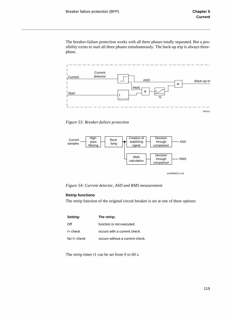
Breaker failure protection (BFP) Chapter 5Current
The breaker-failure protection works with all three phases totally separated. But a pos-sibility exists to start all three phases simultaneously. The back-up trip is always three-phase.
Figure 53: Breaker-failure protection
Figure 54: Current detector, ASD and RMS measurement
Retrip functions
The retrip function of the original circuit breaker is set at one of three options:
The retrip timer t1 can be set from 0 to 60 s.
Setting: The retrip;
Off function is not executed.
I> check occurs with a current check.
No I> check occurs without a current check.
&Back-up tri
& t
RMSt
t1
CurrentdetectorCurrent
Start t
9900010
ASD
High-pass
filtering
Recti-fying
Creation ofstabilizing
signal
Decisionthrough
comparison
RMScalculation
Decisionthrough
comparison
Currentsamples
ASD
RMS
en00000011.vsd
119

Breaker failure protection (BFP) Chapter 5Current
eak-
A trip pulse, tp, is generated with a length of 150 ms.
Back-up trip
The back-up trip delay timer t2 can be set between 0 and 60 s.
A trip pulse, tp, is generated with a length of 150 ms.
Figure 55: Breaker-failure protection
6.3 Design
The breaker failure protection is initiated by the trip commands from the protection functions, either internal to the terminal or from external commands through binary in-puts. The start can be single-phase or three-phase.
The operating values of the three current measuring elements are settable within a wide setting range. The measuring is stabilised against the dc-transient that can cause un-wanted operation at saturated current transformers and correct breaker operation. Time measurement is individual for each phase. Two independent timers are available, T1 for repeated tripping of “own” breaker and T2 which operates trip logic for adjacent brers.
IL1
BFP-STL1
RTL1
IL2
&>1L1
BUTL1STARTL1
BUTL2STARTL2
RTL2L2
tp
>1
tp
&>1 >1
L3RTL3
BUTL3STARTL3
tp
&>1
BFP-STL2BFP-START
IL3
BFP-STL3
BFP-BLOCK
BFP-TRRETL1
BFP-TRRET
BFP-TRRETL2
BFP-TRBU
BFP-TRRETL3
99000050.vsd
tp
IL1
IL2
IL3
120

Breaker failure protection (BFP) Chapter 5Current
in
ed in
of a nc-be ion.
s this
6.4 Calculations
6.4.1 Setting
Human-machine interface (HMI)
The configuration of alternatives or settings to the functions is made on the built-in HMI:
Settings
Functions
Group n
Breaker Failure
The breaker-failure protection can be controlled from the human-machine interface (HMI) by an “Operation” parameter, to be set between alternatives Off/On.
When “Operation” is set to Off, the function becomes inoperative.
The configuration of input and output signals to the function is made on the built-HMI:
Configuration
Function Inputs
Breaker Failure
The inputs and the outputs to and from the breaker-failure protection are presentthe signal list.
The breaker failure protection shall be set by means of a current limit for detectionbreaker failure. The current setting shall be chosen in relation to the protection futions, initiating the breaker failure protection. Normally the current setting should equal to or lower than the most sensitive setting of a residual overcurrent protect
If the retrip function is used a time delay before retrip has to be set. In most casetime delay can be set to zero.
Fixed values
Trip pulse, tp 150 ms, fixed
121

Breaker failure protection (BFP) Chapter 5Current
The time delay of the back-up trip function shall be chosen so that selectivity is main-tained. Consider the following:
t1: Set retrip time delay
tbr: Circuit breaker opening time
BFR reset time
The back-up trip delay t2 shall be set:
(Equation 65)
At the same time it is desired that the back-up trip is done so fast that remote protections will not trip.
t2 t1 tbr margin+ +≥
122
Unbalance protection for capacitor banks (TOCC)
Chapter 5Current
7 Unbalance protection for capacitor banks (TOCC)
7.1 Application
Capacitor banks are made up of individual units which are series and parallel connected. Each unit contains a number of series and parallel connected elements. The individual elements in a capacitor can be separately fused.
If one element is damaged, it will be disconnected by its fuse and the rest of the ele-ments can continue to operate. However, the load on the healthy elements will increase. When a certain number of elements are out of service, the load on the remaining ele-ments becomes so high that the remaining elements will quickly be destroyed.The pur-pose of the unbalance protection is to detect the damage and disconnect the capacitor bank from the network before the the healthy units are overloaded.
The protection is connected to a current transformer which measures the current flow-ing between two normally balanced parts of the capacitor battery. Under normal condi-tions, no fundamental frequency current flows in the interconnection. A low set current stage gives alarm when elements are damaged and current flows in the interconnection. The trip stage is set to disconnect the battery before healthy elements become overload-ed and quickly damaged.
Three-phase capacitor banks are often made up of two identical Y-connected groups. The neutral points are then interconnected via a current transformer which feeds the un-balance protection.
7.2 Functionality
The current measuring element continuously measures the unbalance current (via ana-log input I5) and compares it to the set operate value for the two current stages. A re-cursive Fourier filter ensures immunity to disturbances and harmonic currents. When applied between the neutral points of two identical Y-connected capacitor groups, no false unbalance currents will flow, even for high contents of harmonics in the voltage. The output relay for the low current (alarm) stage operates if the current becomes higher than the set operate value ILow during a time exceeding the set time delay tLow. If the current becomes higher than the set operate value IHigh during a time exceeding the set delay tHigh, the output relay for the high current stage operates.
The input signal TOCC-BLOCK blocks both the low set and the high set function.The stages may also be blocked individually by setting Operation Low = Off respectively Operation High = Off. The setting BlockTOCC = Yes will block the function, during testing.
123
Unbalance protection for capacitor banks (TOCC)
Chapter 5Current
7.3 Calculations
The settings for the TOCC function can be made on the built-in HMI unit:
Settings
Functions
Group n (n=1...4)
CapUnbalance
The settings can also be made by aids of the SMS or PST setting tools.
The current stage I>High is normally set to trip the capacitor battery before any unit is subjected to a voltage increase of 10 % above rated value. The delay tHigh should be set longer than the operate time of the ground fault protection if the primary operate current of stage IHigh is low compared to the ground fault current in the system. The current stage I>Low is normally set to give alarm at 50 % of the set operate current of stage I>High.
The calculation of settings for the unbalance protection function must take into consid-eration how the capacitor bank is built up and it is often made by aids of a computer program.
124

About this chapter Chapter 6Power system supervision
Chapter 6 Power system supervision
About this chapter
This chapter describes the power system supervision functions.
125
Broken conductor check (BRC) Chapter 6Power system supervision
o
phase
ure
en
ion. and
e ter-OR
a trip
1 Broken conductor check (BRC)
1.1 Application
Conventional protections can not detect the broken conductor condition. In REx 5xx terminals this detection is achieved through the broken conductor check function (BRC), consisting of continuous current unsymmetry check on the line where the ter-minal is connected. The detection might also concern possible interruptions in the con-necting circuits between the instrument current transformers and the terminal.
1.2 Functionality
The current-measuring elements continuously measure the three-phase currents. The current unsymmetry signal STI is set to 1 if :
• Any phase current is lower than 80% of the highest current in the remaining twphases
• The highest phase current is greater than the minimum setting value IP>
If the unsymmetrical detection lasts for a period longer than the set time t, a three trip signal BRC--TRIP is emitted.
1.3 Design
The simplified logic diagram of the broken conductor check function is shown in fig56.
The function is disabled (blocked) if:
• The terminal is in TEST status (TEST-ACTIVE is high) and the function has beblocked from the HMI (BlockBRC=Yes)
• The input signal BRC--BLOCK is high
The BRC--BLOCK signal is a blocking signal of the broken conductor check functIt can be connected to a binary input of the terminal in order to receive a block commfrom external devices or can be software connected to other internal functions of thminal itself in order to receive a block command from internal functions. Through gate it can be connected to both binary inputs and internal function outputs.
The output trip signal BRC--TRIP is a three phase trip. It can be used to commandto the circuit breaker or for a signallization.
126
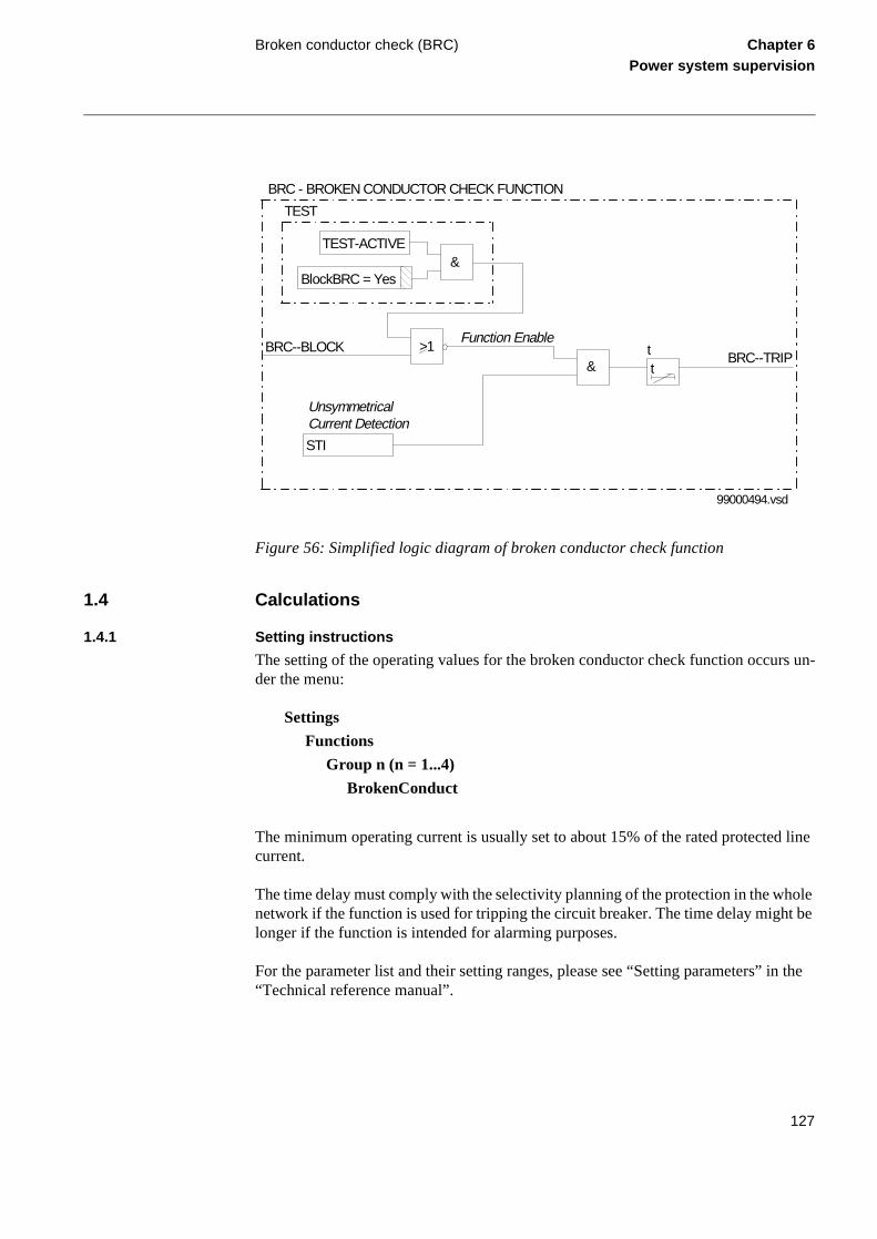
Broken conductor check (BRC) Chapter 6Power system supervision
n the
Figure 56: Simplified logic diagram of broken conductor check function
1.4 Calculations
1.4.1 Setting instructions
The setting of the operating values for the broken conductor check function occurs un-der the menu:
Settings
Functions
Group n (n = 1...4)
BrokenConduct
The minimum operating current is usually set to about 15% of the rated protected line current.
The time delay must comply with the selectivity planning of the protection in the whole network if the function is used for tripping the circuit breaker. The time delay might be longer if the function is intended for alarming purposes.
For the parameter list and their setting ranges, please see “Setting parameters” i“Technical reference manual”.
BRC--BLOCKBRC--TRIP
99000494.vsd
Function Enable
BRC - BROKEN CONDUCTOR CHECK FUNCTION
TEST-ACTIVE&
TEST
BlockBRC = Yes
>1
STI
&
UnsymmetricalCurrent Detection
tt
127
Broken conductor check (BRC) Chapter 6Power system supervision
Setting of the minimum operating current IP>
If the rated current of the protected line is IL, then the primary set value IsPRIMwill be:
(Equation 66)
The secondary setting value IsSEC is:
(Equation 67)
The relay setting value IP> is given in percentage of the secondary base current value, I1b, associated to the current transformer input I1. The value for IP> is given from this formula:
(Equation 68)
and this is the value that has to be set in the terminal.
Set this value under the setting menu:
Where:
ISEC is the secondary rated current of the main CT and
IPRIM is the primary rated current of the main CT.
IsPRIM 0 15, IL⋅=
IsSEC
ISEC
IPRIM-------------- IsPRIM⋅=
IP>IsSEC
I1b--------------- 100⋅=
128

Broken conductor check (BRC) Chapter 6Power system supervision
Settings
Functions
Group n
BrokenConduct
on the value IP>.
So it is obtained:
(Equation 69)
(Equation 70)
This is why the default setting for IP> is 10%.
Setting of time delay t
Set the time delay of the function, t, under the setting menu:
Settings
Functions
Group n
BrokenConduct
on the value t.
Note!
Usually IPRIM is chosen to be 1.4 times the rated line current (IPRIM = 1.4 . IL) and isset to the relay rated current, equal to the secondary rated current of the main CT (I1b= ISEC).
IP>
ISEC
IPRIM-------------- IsPRIM⋅
I1b------------------------------------- 100⋅=
IP>
ISEC1.4 I⋅ L----------------- 0 15, IL⋅ ⋅
ISEC-------------------------------------------- 100⋅
10.7 %==
129
Overload supervision (OVLD) Chapter 6Power system supervision
an the
n in
en
2 Overload supervision (OVLD)
2.1 Application
The overload supervision function sends an alarm signal when the current exceeds the set level for longer than a pre-set time. The operating level of the current measuring el-ement can be set to the maximum, accepted, continuous current. So operators are alerted if the primary system operates in a dangerous overload mode. A typical application is the signalling of the overload of the current transformers connected to the terminal, as they usually can withstand a small current beyond their rated current.
2.2 Functionality
The current-measuring elements continuously measure the three phase currents, and compare them with the set values. Fourier’s recursive filter filters the current signals.
The logical values of the following signals become equal to 1, if the measured current in any phase exceeds the pre-set value:
• STIL1
• STIL2
• STIL3
If any of the three phase currents exceeds the set value IP> for a period longer thdelay time t, then the trip signal OVLD-TRIP is emitted.
2.3 Design
The simplified logic diagram of the time delayed phase overload function is showfigure 57.
The function is disabled (blocked) if:
• The terminal is in TEST status (TEST-ACTIVE is high) and the function has beblocked from the HMI (BlockOVLD=Yes)
• The input signal OVLD-BLOCK is high
130
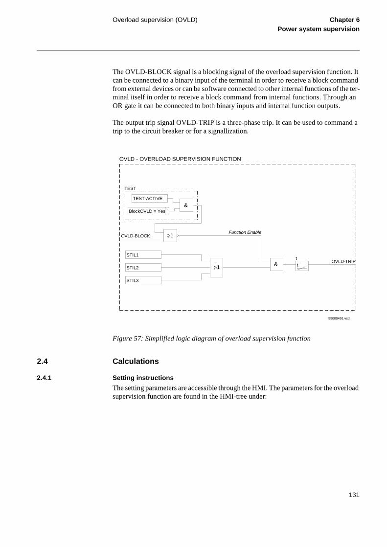
Overload supervision (OVLD) Chapter 6Power system supervision
The OVLD-BLOCK signal is a blocking signal of the overload supervision function. It can be connected to a binary input of the terminal in order to receive a block command from external devices or can be software connected to other internal functions of the ter-minal itself in order to receive a block command from internal functions. Through an OR gate it can be connected to both binary inputs and internal function outputs.
The output trip signal OVLD-TRIP is a three-phase trip. It can be used to command a trip to the circuit breaker or for a signallization.
Figure 57: Simplified logic diagram of overload supervision function
2.4 Calculations
2.4.1 Setting instructions
The setting parameters are accessible through the HMI. The parameters for the overload supervision function are found in the HMI-tree under:
OVLD-BLOCK
99000491.vsd
OVLD - OVERLOAD SUPERVISION FUNCTION
TEST-ACTIVE
&
TEST
BlockOVLD = Yes
>1
STIL1
STIL2
STIL3
OVLD-TRIP>1 t
t
Function Enable
&
131
Overload supervision (OVLD) Chapter 6Power system supervision
Settings
Functions
Group n (n = 1...4)
OverLoad
The current level set should be above the maximum permissible load current. Consider the accuracy class of the used instrument current transformers and the specified accu-racy of the current measuring elements in the REx 5xx terminals.
The corresponding time delay must comply with the selectivity planning of the protec-tion in the whole network, and with the permissible overloading of the conductors, if the function is used for tripping the circuit breaker. The above settings might change to a lower current value and longer time delay if the function serves only for alarming and not for tripping purposes.
Setting of operating current IP>
The relay setting value IP> is given in percentage of the secondary base current value, I1b , associated to the current transformer.
If IsSEC is the secondary current operating value of the function, then the relay setting value IP> is given from this formula:
(Equation 71)
and this is the value that has to be set in the terminal.
IP>IsSEC
I1b--------------- 100⋅=
132
About this chapter Chapter 7Secondary system supervision
Chapter 7 Secondary system supervision
About this chapter
This chapter describes the secondary system supervision functions.
133
Current circuit supervision (CTSU) Chapter 7Secondary system supervision
urrent If an cked
ema-rents ient
nt un-n the
nce ult tion. n not r.
hase al
ful-
t
10 ms
1 Current circuit supervision (CTSU)
1.1 Application
The correct operation of a protection depends on correct information about the primary value of currents and voltages. When currents from two independent 3-phase sets of CT’s, or CT cores, measuring the same primary currents are available, a reliable ccircuit supervision can be arranged by comparing the currents from the two sets.error in any CT circuit is detected, the protection functions concerned are to be bloand an alarm given.
In case of large currents, unequal transient saturation of CT cores with different rnence or different saturation factor may result in differences in the secondary curfrom the two CT sets. Unwanted blocking of protection functions during the transperiod must be avoided.
The supervision function must be sensitive and have short operate time to prevewanted tripping from fast-acting, sensitive numerical protections in case of errors icurrent circuits.
Note that the same current input transformer (I5) in REx 5xx is used for the referecurrent Iref of the CT supervision, the residual current from the parallel line for the falocator and, dependent on setting I4 or I5, maybe for the earth-fault protection funcHence, when the CT supervision function is used, the other functions mentioned cabe used. Also the settings Xm0 = 0 and Rm0 = 0 must be used for the fault locato
1.2 Functionality
The supervision function compares the numerical value of the sum of the three pcurrents |ΣIphase| (current inputs I1, I2 and I3) and the numerical value of the residucurrent |Iref| (current input I5) from another current transformer set, see figure 58.
The CTSU-FAIL output will be set to a logical one when the following criteria are filled:
• The numerical value of the difference |ΣIphase| – |Iref| is higher than 80% of the nu-merical value of the sum |ΣIphase| + |Iref|.
• The numerical value of the current |ΣIphase| – |Iref| is equal to or higher than the seoperate value IMinOp (5 - 100% of I1b).
• No phase current has exceeded 1.5 times rated relay current I1b during the last
• The current circuit supervision is released by setting Operation = On.
134

Current circuit supervision (CTSU) Chapter 7Secondary system supervision
The CTSU-FAIL output remains activated 100 ms after the AND-gate resets when be-ing activated for more than 20 ms. If the CTSU-FAIL lasts for more than 150 ms a CTSU-ALARM will be issued. In this case the CTSU-FAIL and CTSU-ALARM will remain activated 1 s after the AND-gate resets. This prevents unwanted resetting of the blocking function when phase current supervision element(s) operate, e.g. during a fault.
Figure 58: Simplified logic diagram for the current circuit supervision
The operate characteristic is percentage restrained, see figure 59.
∑
1,5 x Ir
∑+
-
∑++
>1
&
∑+
-
I>
OPERATION
CTSU-BLOCK
III
L1
L2
L3
Iref
10 ms
100 ms20 ms
CTSU-FAIL
CTSU-ALARM
>1
99000067.vsd
1 s150 ms
x 0,8
135
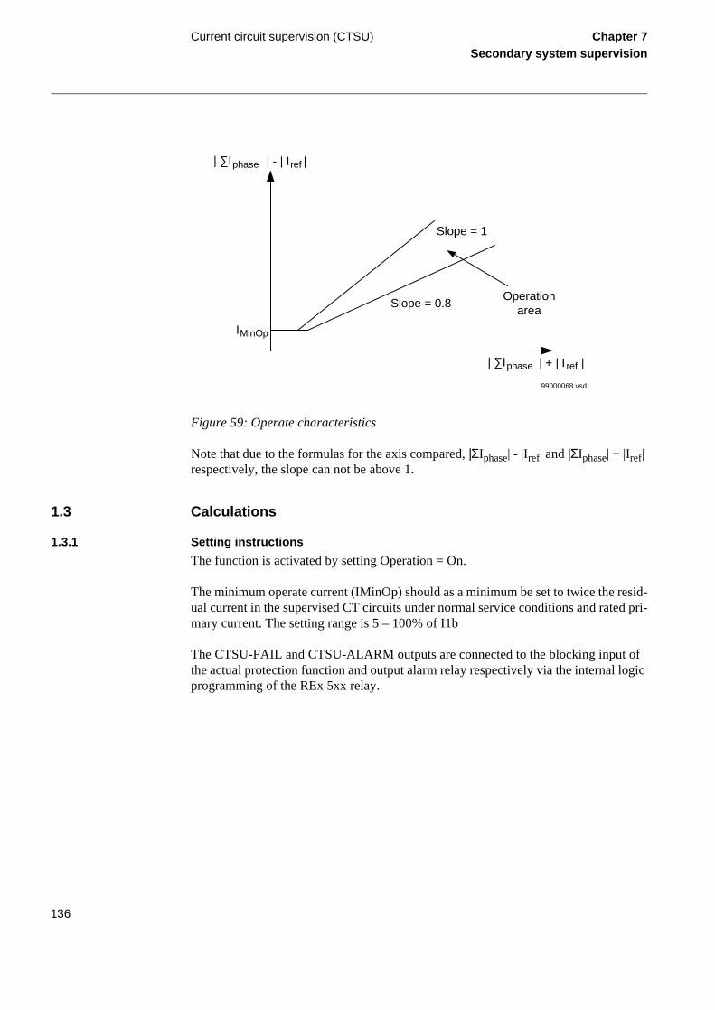
Current circuit supervision (CTSU) Chapter 7Secondary system supervision
of ogic
Figure 59: Operate characteristics
Note that due to the formulas for the axis compared, |ΣIphase| - |Iref| and |ΣIphase| + |Iref| respectively, the slope can not be above 1.
1.3 Calculations
1.3.1 Setting instructions
The function is activated by setting Operation = On.
The minimum operate current (IMinOp) should as a minimum be set to twice the resid-ual current in the supervised CT circuits under normal service conditions and rated pri-mary current. The setting range is 5 – 100% of I1b
The CTSU-FAIL and CTSU-ALARM outputs are connected to the blocking input the actual protection function and output alarm relay respectively via the internal lprogramming of the REx 5xx relay.
Slope = 0.8
Slope = 1
Operationarea
IMinOp
99000068.vsd
phase ref| ∑I | - | I |
phase ref| ∑I | + | I |
136

About this chapter Chapter 8Control
Chapter 8 Control
About this chapter
This chapter describes the control functions.
137
Automatic reclosing function (AR) Chapter 8Control
1 Automatic reclosing function (AR)
1.1 Application
Automatic reclosing (AR) is a well-established method to restore the service of a power line after a transient line fault. The majority of line faults are flashover arcs, which are transient by nature. When the power line is switched off by operation of line protection and line breakers, the arc de-ionises and recovers voltage withstand at a somewhat vari-able rate. So a certain line dead time is needed. But then line service can resume by the auto-reclosing of the line breakers. Select the length of the dead time to enable good probability of fault arc de-ionisation and successful reclosing.
For the individual line breakers and auto-reclosing equipment, the Auto-reclose open time (AR open time) expression is used. At simultaneous tripping and reclosing at the two line ends, Auto-reclose open time equals approximaltely the dead time of the line. Otherwise these two times may differ.
In case of a permanent fault, the line protection trips again at reclosing to clear the fault.
138

Automatic reclosing function (AR) Chapter 8Control
Figure 60: Single-shot auto-reclosing at a permanent fault
In a bay with one circuit breaker only one terminal is normally provided with one AR function.
Single-phase tripping and single-phase reclosing is a way to limit the effect of a single-phase line fault to system operation. Especially at higher voltages, the majority of line faults are of the single-phase type. The method is of particular value to maintain system stability in systems with limited meshing or parallel routing. It requires individual op-eration of each phase of the breakers, which is common at the higher transmission volt-ages.
A somewhat longer dead time may be required at single-phase reclosing compared to high-speed three-phase reclosing, due to influence on the fault arc from voltage and cur-rent of the non-tripped phases.
Open
Closed
Operate time
Lineprotection
Circuitbreaker
Break time
Trip
com
man
d
Con
tact
s se
para
ted
Are
ext
ingu
ishe
rs
Fault duration AR open time for breaker Fault duration
Res
ets
Inst
at o
f fau
lt
Ope
rate
s
Break timeClosing time
Operate time
Fau
lt
Ope
rate
s
Res
ets
Clo
se c
omm
and
Con
tact
clo
sed
Set AR open time Reclaim timeAuto-reclosing
function
Sta
rt A
R
Rec
losi
ngco
mm
and
AR
res
et
99000118.vsd
139
Automatic reclosing function (AR) Chapter 8Control
tem. idual clos-
three-ee-
auto-eed
on-ose input ns).
ction
eter ON
There is also a possibility to trip and reclose two of the circuit breaker poles, in case of faults when two out of the three phases are involved and parallel lines are in service. This type of faults is less common compared to single phase to earth faults, but more common than three phase faults.
In order to maximize the availability of the power system there is a possibility to chose single pole tripping and auto-reclosing at single phase faults, two pole tripping and auto-reclosing at faults involving two phases and three pole tripping and auto-reclosing at three phase faults.
During the single pole open time there will be an equivalent “series”-fault in the sysAs a consequence there will be a flow of zero sequence current. Therefor the rescurrent protections must be co-ordinated with the single pole tripping and auto-reing.
The reclosing function can be selected to perform single-phase, two-phase and/orphase reclosing from six single-shot to multiple-shot reclosing programs. The thrphase auto-reclose open time can be set to give either high-speed auto-reclosing(HSAR) or delayed auto-reclosing (DAR). In the reclosing programs the delayed reclosing (DAR) is always a three pole trip and reclosing, even if the first high-spreclosing is a single pole action.
1.2 Functionality
The AR function is a logical function built up from logical elements. It operates in cjunction with the trip output signals from the line protection functions, the OK to cloutput signals from the synchrocheck and energizing check function, and binary signals (for circuit breaker position/status, or from other external protection functio
In the AR logic a number of parameters can be set to adjust the auto-reclosing funto the desired requirements. Examples are:
• Number of AR attempts
• AR programs
• Open times for different AR attempts
Start and control of the auto-reclosing
The automatic operation of the auto-reclosing function is controlled by the paramOperation and the input signals as described above. When it is on, the AR01-SEToutput is high (active). See Function block diagrams.
140

Automatic reclosing function (AR) Chapter 8Control
The auto-reclosing function is activated at a protection trip by the AR01-START input signal. At repeated trips, this signal is activated again to make the reclosing program continue.
There are a number of conditions for the start to be accepted and a new cycle started. After these checks, the start signal is latched in and the Started state signal is activated. It can be interrupted by certain events.
Extended AR open time, shot 1
The purpose of this function is to adapt the length of the AR Open time to the possibility of non-simultaneous tripping at the two line ends. If a permissive communication scheme is used and the permissive communication channel (for example, PLC, power-line carrier) is out of service at the fault, there is a risk of sequential non-simultaneous tripping. To ensure a sufficient line dead time, the AR open time is extended by 0.4 s. The input signal AR01-PLCLOST is checked at tripping. See Function block diagrams. Select this function (or not) by setting the Extended t1 parameter to On (or Off).
Long trip signal
During normal circumstances, the trip command resets quickly due to fault clearing. The user can set a maximum trip pulse duration by tTrip. At a longer trip signal, the AR open dead time is extended by Extend_t1. If the Extended t1 = Off, a long trip signal interrupts the reclosing sequence in the same way as AR01-INHIBIT.
Reclosing programs
The reclosing programs can be performed with up to maximum four reclosing attempts (shots), selectable with the NoOfReclosing parameter. The first program is used at pure 3-phase trips of breakers and the other programs are used at 1-, 2- or 3-phase trips of breakers.
3ph
3-phase reclosing, one to four attempts (NoOfReclosing parameter). The output AR01-P3P is always high (=1).
A trip operation is made as a three-phase trip at all types of fault. The reclosing is as a three-phase reclosing in program 1/2/3ph, described below.
1/2/3ph
1-phase, 2-phase or 3-phase reclosing in the first shot.
For the example, one-shot reclosing for 1-phase, 2-phase or 3-phase, see Figures in Function block diagrams. Here, the AR function is assumed to be On and Ready. The breaker is closed and the operation gear ready (manoeuvre spring charged etc.). Only the 1-phase and 3-phase cases are described.
141

Automatic reclosing function (AR) Chapter 8Control
AR01-START is received and sealed-in at operation of the line protection. The AR01-READY output is reset (Ready for a new AR cycle).
If AR01-TR2P (2-phase trip) is low and AR01-TR3P (3-phase trip) is:
Immediately after the start-up of the reclosing and tripping of the breaker, the input (see Function block diagrams) AR01-CBCLOSED is low (possibly also AR01-CBREADY at type OCO). The AR Open-time timer, t1 1Ph or t1, keeps on running.
At the end of the set AR open time, t1 1Ph or t1, the respective SPTO or TPTO (single-phase or three-phase AR time-out, see Function block diagrams) is activated and goes on to the output module for further checks and to give a closing command to the circuit breaker.
At any kind of trip, the operation is as already described, program 1/2/3ph. If the first reclosing attempt fails, a 3-phase trip will be issued and 3-phase reclosings can follow, if selected. Maximum three additional attempts can be done (according to the NoOfRe-closing parameter).
1/2ph
1-phase or 2-phase reclosing in the first shot.
At 1-phase or 2-phase trip, the operation is as in above described example, program 1/2/3ph. If the first reclosing attempt fails, a 3-phase trip will be issued and 3-phase re-closings can follow, if selected. Maximum three additional attempts can be done (ac-cording to the NoOfReclosing parameter).
At 3-phase trip, TR2P low and TR3P high, the AR will be blocked and no reclosing takes place.
1ph + 1*2ph
1-phase or 2-phase reclosing in the first shot.
low, the timer for 1-phase reclosing open time t1 1Ph is started and the AR01-1PT1 output (auto-reclosing 1-phase, shot 1, in progress) is activated. It can be used to suppress Pole disagreement and Earth-fault protection during the 1-phase open interval.
high, the timer for 3-phase AR open time, t1, is started (instead of t1 1Ph) and AR01-T1 is set (auto-reclosing 3-phase, shot 1, in progress). While either t1 1Ph or t1 is running, the output AR01-INPROGR is activated.
142
Automatic reclosing function (AR) Chapter 8Control
At 1-phase trip (TR2P low and TR3P low), the operation is as in above described ex-ample, program 1/2/3ph. If the first reclosing attempt fails, a 3-phase trip will be issued and 3-phase reclosings can follow, if selected. Maximum three additional attempts can be done (according to the NoOfReclosing parameter).
At 2-phase trip (TR2P high and TR3P low), the operation is similar as above. But, if the first reclosing attempt fails, a 3-phase trip will be issued and the AR will be blocked. No more attempts take place!
At 3-phase trip, TR2P low and TR3P high, the AR will be blocked and no reclosing takes place.
1/2ph + 1*3ph
1-phase, 2-phase or 3-phase reclosing in the first shot.
At 1-phase or 2-phase trip, the operation is as described above. If the first reclosing at-tempt fails, a 3-phase trip will be issued and 3-phase reclosings can follow, if selected. Maximum three additional attempts can be done (according to the NoOfReclosing pa-rameter).
At 3-phase trip, the operation is similar as above. But, if the first reclosing attempt fails, a 3-phase trip will be issued and the AR will be blocked. No more attempts take place!
1ph + 1*2/3ph
1-phase, 2-phase or 3-phase reclosing in the first shot.
At 1-phase trip, the operation is as described above. If the first reclosing attempt fails, a 3-phase trip will be issued and 3-phase reclosings can follow, if selected. Maximum three additional attempts can be done (according to the NoOfReclosing parameter).
At 2-phase or 3-phase trip, the operation is similar as above. But, if the first reclosing attempt fails, a 3-phase trip will be issued and the AR will be blocked. No more attempts take place!
Table 8: Type of reclosing for different programs
Program 1st attempt 2-4th attempt
3ph 3ph 3ph
1/2/3ph 1ph 3ph
2ph 3ph
3ph 3ph
1/2ph 1ph 3ph
143
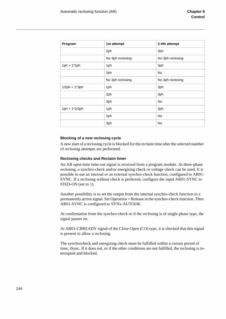
Automatic reclosing function (AR) Chapter 8Control
Blocking of a new reclosing cycle
A new start of a reclosing cycle is blocked for the reclaim time after the selected number of reclosing attempts are performed.
Reclosing checks and Reclaim timer
An AR open-time time-out signal is received from a program module. At three-phase reclosing, a synchro-check and/or energising check or voltage check can be used. It is possible to use an internal or an external synchro-check function, configured to AR01-SYNC. If a reclosing without check is preferred, configure the input AR01-SYNC to FIXD-ON (set to 1).
Another possibility is to set the output from the internal synchro-check function to a permanently active signal. Set Operation = Release in the synchro-check function. Then AR01-SYNC is configured to SYNx-AUTOOK.
At confirmation from the synchro-check or if the reclosing is of single-phase type, the signal passes on.
At AR01-CBREADY signal of the Close-Open (CO) type, it is checked that this signal is present to allow a reclosing.
The synchrocheck and energizing check must be fulfilled within a certain period of time, tSync. If it does not, or if the other conditions are not fulfilled, the reclosing is in-terrupted and blocked.
2ph 3ph
No 3ph reclosing No 3ph reclosing
1ph + 1*2ph 1ph 3ph
2ph No
No 3ph reclosing No 3ph reclosing
1/2ph + 1*3ph 1ph 3ph
2ph 3ph
3ph No
1ph + 1*2/3ph 1ph 3ph
2ph No
3ph No
Program 1st attempt 2-4th attempt
144

Automatic reclosing function (AR) Chapter 8Control
The Reclaim-timer defines a period from the issue of a reclosing command, after which the reclosing function is reset. Should a new trip occur within this time, it is treated as a continuation of the first fault. When a closing command is given (Pulse AR), the re-claim timer is started.
There is an AR State Control, see Function block diagrams, to track the actual state in the reclosing sequence.
Pulsing of CB closing command
The circuit breaker closing command, AR01-CLOSECB, is made as a pulse with a du-ration, set by the tPulse parameter. For circuit breakers without an anti-pumping func-tion, the closing-pulse-cutting described below can be used. It is selected by means of the CutPulse parameter (set to On). In case of a new trip pulse, the closing pulse will be cut (interrupted). But the minimum length of the closing pulse is always 50 ms.
At the issue of a reclosing command, the associated reclosing operation counter is also incremented. There is a counter for each type of reclosing and one for the total number of reclosings. See Function block diagrams.
Transient fault
After the reclosing command, the reclaim timer keeps running for the set time. If no tripping occurs within this time, tReclaim, the auto-reclosing function will be reset. The circuit breaker remains closed and the operating gear ready (manoeuvre spring is re-charged). AR01-CBCLOSED = 1 and AR01-CBREADY = 1.
After the reclaim time, the AR state control resets to original rest state, with AR01-SE-TON = 1, AR01-READY = 1 and AR01-P1P = 1 (depending on the selected program). The other AR01 outputs = 0.
Unsuccessful signal
Normally the signal AR01-UNSUC appears when a new start is received after the last reclosing attempt has been made. See Function block diagrams. It can be programmed to appear at any stage of a reclosing sequence by setting the parameter UnsucMode = On. The UNSUC signal is attained after the time tUnsuc.
Permanent fault
If a new trip takes place after a reclosing attempt and a new AR01-START or AR01-TRSOTF signal appears, the AR01-UNSUC (Reclosing unsuccessful) is activated. The timers for the first reclosing attempt (t1 1Ph, t1 2Ph and t1) cannot be started.
Depending on the PulseCut parameter setting, the closing command may be shortened at the second trip command.
145
Automatic reclosing function (AR) Chapter 8Control
After time-out of the reclaim timer, the auto reclosing function resets, but the circuit breaker remains open (AR01-CBCLOSED = 0, AR01-CBREADY = 1). Thus the re-closing function is not ready for a new reclosing cycle. See Function block diagrams and Sequence examples.
Automatic confirmation of programmed reclosing attempts
The auto-recloser can be programmed to continue with reclosing attempts two to four (if selected) even if the start signals are not received from the protection functions, but the breaker is still not closed. See figure in Function block diagrams. This is done by setting the parameter AutoCont = On and the wait time tAutoWait to desired length.
1.3 Calculations
1.3.1 Configuration and setting
The signals are configured in the CAP 531 configuration tool.
The parameters for the auto-reclosing function are set through the local HMI at:
Settings
Functions
Group n
AutoRecloser
AutoRecloser n
Recommendations for input signals
See figure 61 and the default configuration for examples.
AR01-START
Should be connected to the protection function trip output which shall start the auto-re-closer. It can also be connected to a binary input for start from an external contact. A logical OR gate can be used to multiply the number of start sources.
AR01-ON and AR01-OFF
May be connected to binary inputs for external control.
146
Automatic reclosing function (AR) Chapter 8Control
AR01-INHIBIT
Can be connected to binary inputs, to block the AR from a certain protection, such as a line connected shunt reactor, transfer trip receive or back-up protection or breaker-fail-ure protection.
AR01-CBCLOSED and AR01-CBREADY
Must be connected to binary inputs, for pick-up of the breaker signals. If the external signals are of Breaker-not-ready type, uncharged etc., an inverter can be configured be-fore CBREADY.
AR01-SYNC
Is connected to the internal synchro-check function if required. It can also be connected to a binary input. If neither internal nor external synchronising or energising check (dead line check) is required, it can be connected to a permanent 1 (high), by connection to FIXD-ON.
AR01-PLCLOST
Can be connected to a binary input, when required.
AR01-TRSOTF
Can be connected to the internal line protection, distance protection, trip switch-onto-fault.
AR01-STTHOL
Start of thermal overload protection signal. Can be connected to OVLD-TRIP to block the AR at overload.
AR01-TR2P and AR01-TR3P
Are connected to the function block TRIP or to binary inputs. The protection functions that give two-phase or three-phase trips are supposed to be routed via that function.
147
Automatic reclosing function (AR) Chapter 8Control
Other
The other input signals can be connected as required.
Recommendations for output signals
See figure 61 and the default configuration for examples.
AR01-READY
Can be connected to the Zone extension of a line protection. It can also be used for in-dication, if required.
AR01-1PT1 and 2PT1
1-phase and 2-phase reclosing in progress is used to temporarily block an Earth-fault protection and/or a Pole disagreement function during the 1-phase or 2-phase open in-tervals.
AR01-CLOSECB
Connect to a binary output relay for circuit breaker closing command.
AR01-P3P
Prepare 3-phase trip: Connect to TRIP-P3PTR.
AR01-P1P
Permit 1-phase trip: Can be connected to a binary output for connection to external pro-tection or trip relays. In case of total loss of auxiliary voltage, the output relay drops and does not allow 1-phase trip. If needed to invert the signal, it can be made by a breaking contact of the output relay.
Other
The other output signals can be connected for indication, disturbance recording etc., as required.
148
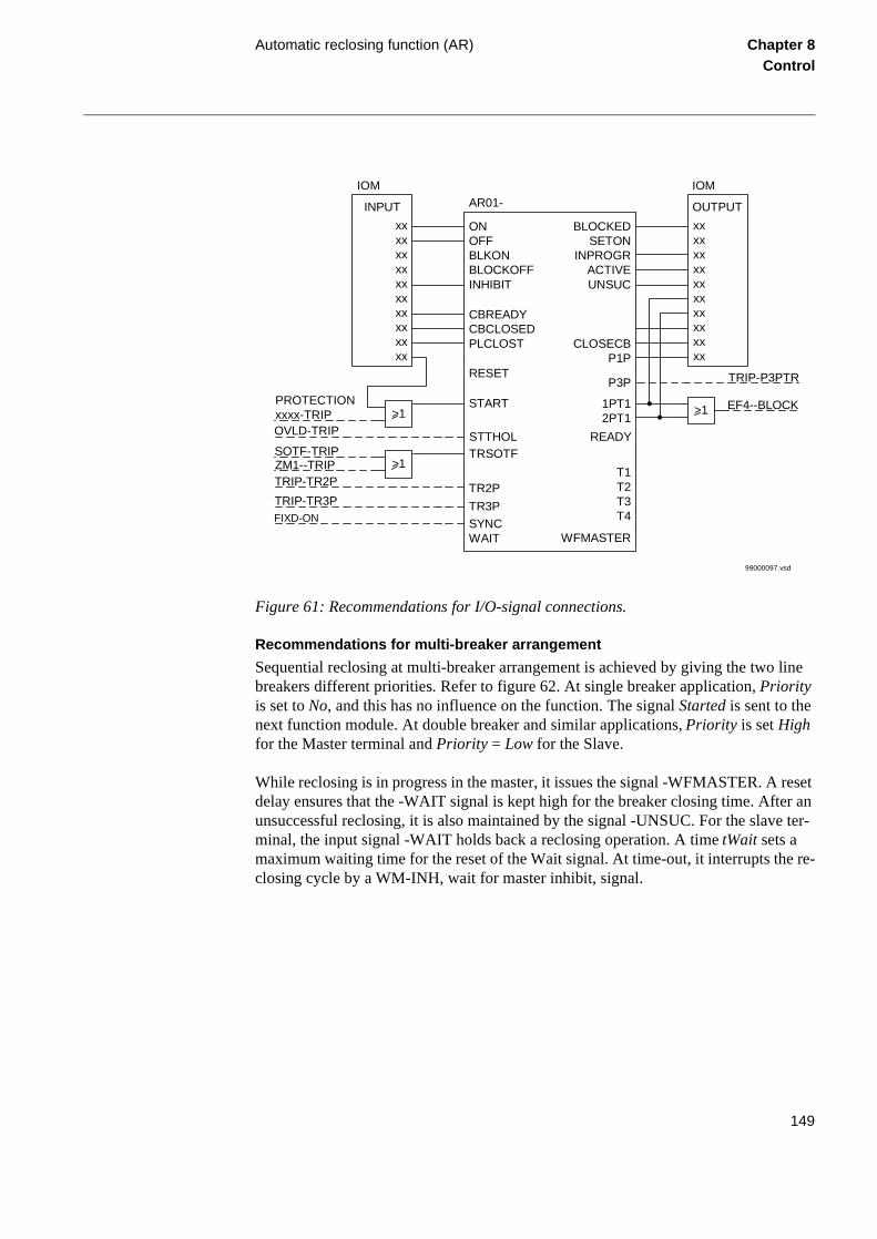
Automatic reclosing function (AR) Chapter 8Control
Figure 61: Recommendations for I/O-signal connections.
Recommendations for multi-breaker arrangement
Sequential reclosing at multi-breaker arrangement is achieved by giving the two line breakers different priorities. Refer to figure 62. At single breaker application, Priority is set to No, and this has no influence on the function. The signal Started is sent to the next function module. At double breaker and similar applications, Priority is set High for the Master terminal and Priority = Low for the Slave.
While reclosing is in progress in the master, it issues the signal -WFMASTER. A reset delay ensures that the -WAIT signal is kept high for the breaker closing time. After an unsuccessful reclosing, it is also maintained by the signal -UNSUC. For the slave ter-minal, the input signal -WAIT holds back a reclosing operation. A time tWait sets a maximum waiting time for the reset of the Wait signal. At time-out, it interrupts the re-closing cycle by a WM-INH, wait for master inhibit, signal.
ONOFFBLKONBLOCKOFFINHIBIT
BLOCKEDSETON
INPROGRACTIVEUNSUC
CLOSECBP1P
CBREADYCBCLOSEDPLCLOST
T1T2T3T4
WFMASTER
RESET
START
P3P
1PT12PT1
STTHOL READYTRSOTF
TR2P
TR3P
SYNCWAIT
INPUT
xxxxxxxxxxxxxxxxxxxx
>1
>1
OUTPUT
xxxxxxxxxxxxxxxxxxxx
>1PROTECTIONxxxx-TRIPOVLD-TRIP
SOTF-TRIPZM1--TRIPTRIP-TR2P
TRIP-TR3PFIXD-ON
TRIP-P3PTR
EF4--BLOCK
IOM IOMAR01-
99000097.vsd
149
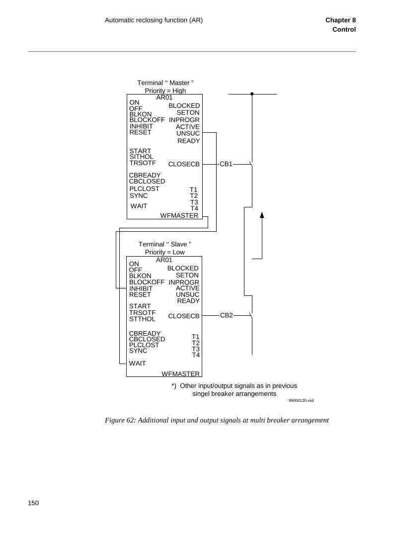
Automatic reclosing function (AR) Chapter 8Control
Figure 62: Additional input and output signals at multi breaker arrangement
99000120.vsd
ACTIVEUNSUCREADY
CLOSECB
T2T3
WAIT
PLCLOSTCBCLOSEDCBREADY
TRSOTFSITHOLSTART
RESET
BLOCKOFFBLKONOFFON BLOCKED
SETONINPROGR
T1
T4
SYNC
INHIBIT
Terminal ‘‘ Master ”Priority = High
AR01
ACTIVEUNSUCREADY
CLOSECB
T2T3
WAIT
PLCLOSTCBCLOSEDCBREADY
TRSOTFSTTHOL
START
RESET
BLOCKOFFBLKONOFFON
BLOCKEDSETON
INPROGR
T1
T4SYNC
INHIBIT
Terminal ‘‘ Slave ”Priority = Low
AR01
CB1
CB2
WFMASTER
WFMASTER
*) Other input/output signals as in previoussingel breaker arrangements
150

Automatic reclosing function (AR) Chapter 8Control
Settings
Number of reclosing attempts: 1 to 4 attempts can be chosen. In most cases 1 attempt is sufficient as the majority of arcing faults will cease after the first reclosing shot. In pow-er systems with many faults caused by other phenomena than lightning, for example wind, it can be motivated with more than one reclosing attempt.
There are six different possibilities in the selection of reclosing programs. What type of first shot reclosing shall be made, and for which types of faults? In completely meshed power systems it is often acceptable to use three pole auto-reclosing for all fault types, as first shot. In power systems with few parallel paths single pole auto-reclosing should be considered, in order to avoid reclosing in a phase opposition situation. In such sys-tems auto-reclosing should be allowed for single phase faults only. It must be remem-bered that there will be zero sequence current flow in the power system during the single pole reclosing open time.
If a permissive channel is used between the line ends, and the availability of the com-munication channel is considered to be low, extended dead time in case of loss of the channel should be used.
Due to the secondary arc at single pole trip and auto-reclosing, the extinguishing time for the arc will be longer than for three pole trip and auto-reclosing. Typical required dead time for single pole trip and reclosing: 800 ms. Typical required dead time for three pole trip and reclosing: 400 ms. Different local phenomena, such as moisture, salt, pollution, etc. can influence the required dead time. Different open time for first auto-reclosing shot can be chosen for single pole (t1 1Ph), two pole (t1 2PH) and three pole (t1).
The open time for the three pole delayed auto-reclosing shots can be set individually (t2, t3 and t4). This setting can in some cases be restricted by national regulations.
In case of reclosing based on synchrocheck a maximum wait time (tSync) can be set. If the synchrocheck does not allow reclosing within this set time there will be no autore-closing. This setting must be matched against the setting of the synchrocheck function. The operate time of the synchrocheck is mainly dependent on the setting angle differ-ence. A typical operation time is about 200 ms. If the system will start to oscillate during the dead time, there can be some time before the synchronising quantities can be accept-ed for reclosing. This can be checked by means of dynamic simulations. As a base rec-ommendation tSync can be set to 2.0 s.
The breaker closing pulse length (tPulse) can be chosen with some margin longer that the shortest allowed pulse for the breaker (see breaker data).
The tReclaim setting must be chosen so that all autoreclosing shots can be completed.
151

Automatic reclosing function (AR) Chapter 8Control
The setting tTrip is used for blocking of autoreclosing in case of long trip duration. This can be the consequence of an unwanted permanent trip signal or a breaker failure.
In case of two or more autoreclosing modules only one shall be chosen as maser (prior-ity high). The others should have priority low. In case of one breaker only none priority is chosen.
152

Single command (CD) Chapter 8Control
2 Single command (CD)
2.1 Application
The terminals may be provided with a function to receive signals either from a substa-tion automation system or from the local human-machine interface, HMI. That receiv-ing function block has outputs that can be used, for example, to control high voltage apparatuses in switchyards. For local control functions, the local HMI can also be used. Together with the configuration logic circuits, the user can govern pulses or steady out-put signals for control purposes within the terminal or via binary outputs.
Figure 63 shows an application example of how the user can, in an easy way, connect the command function via the configuration logic circuit to control a high-voltage ap-paratus. This type of command control is normally performed by a pulse via the binary outputs of the terminal. Figure 63 shows a close operation, but an open operation is per-formed in a corresponding way without the synchro-check condition.
Figure 63: Application example showing a logic diagram for control of a circuit break-er via configuration logic circuits
Figure 64 and figure 65 show other ways to control functions, which require steady On/Off signals. The output can be used to control built-in functions or external equipment.
SinglecommandfunctionCDxxSingleCmdFunc
CmdOuty
OUTy
MODE
Close CB1
2
&User-definedconditions
Synchro-check
Configuration logic circuits
200 ms
99000422.vsd
153
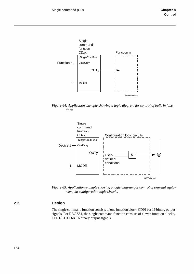
Single command (CD) Chapter 8Control
Figure 64: Application example showing a logic diagram for control of built-in func-tions
Figure 65: Application example showing a logic diagram for control of external equip-ment via configuration logic circuits
2.2 Design
The single command function consists of one function block, CD01 for 16 binary output signals. For REC 561, the single command function consists of eleven function blocks, CD01-CD11 for 16 binary output signals.
SinglecommandfunctionCDxxSingleCmdFunc
CmdOuty
OUTy
MODE
Function n
1
99000423.vsd
Function n
SinglecommandfunctionCDxxSingleCmdFunc
CmdOuty
OUTy
MODE
Device 1
1
User-definedconditions
Configuration logic circuits
99000424.vsd
&
154

Single command (CD) Chapter 8Control
vel,
sent
the cted
ution
ol axi-
uilt-nal.
1 con-
clud-of the
The output signals can be of the types Off, Steady, or Pulse. The setting is done on the MODE input, common for the whole block, from the CAP 531 configuration tool.
• 0 = Off sets all outputs to 0, independent of the values sent from the station lethat is, the operator station or remote-control gateway.
• 1 = Steady sets the outputs to a steady signal 0 or 1, depending on the valuesfrom the station level.
• 2 = Pulse gives a pulse with one execution cycle duration, if a value sent fromstation level is changed from 0 to 1. That means that the configured logic conneto the command function block may not have a cycle time longer than the execcycle time for the command function block.
The outputs can be individually controlled from the operator station, remote-contrgateway, or from the local HMI. Each output signal can be given a name with a mmum of 13 characters from the CAP 531 configuration tool.
The output signals, here OUT1 to OUT16, are then available for configuration to bin functions or via the configuration logic circuits to the binary outputs of the termi
2.3 Calculations
2.3.1 Setting
The setting parameters for the single command function are set from the CAP 53figuration tool.
Parameters to be set are MODE, common for the whole block, and CmdOuty - ining the name for each output signal. The MODE input sets the outputs to be one types Off, Steady, or Pulse.
155

Multiple command (CM) Chapter 8Control
vel,
sent
the cted
ution
can e for 531.
uilt-nal.
3 Multiple command (CM)
3.1 Application
The terminals may be provided with a function to receive signals either from a substa-tion automation system or from other terminals via the interbay bus. That receiving function block has 16 outputs that can be used, together with the configuration logic cir-cuits, for control purposes within the terminal or via binary outputs. When it is used to communicate with other terminals, these terminals have a corresponding event function block to send the information.
3.2 Design
General
One multiple command function block CM01 with fast execution time also named Bi-nary signal interbay communication, high speed and/or 79 multiple command function blocks CM02-CM80 with slower execution time are available in the REx 5xx terminals as options. For REC 561 the seventy-nine multiple command function blocks CM02-CM80 with slow execution time is included in basic.
The output signals can be of the types Off, Steady, or Pulse. The setting is done on the MODE input, common for the whole block, from the CAP 531 configuration tool.
• 0 = Off sets all outputs to 0, independent of the values sent from the station lethat is, the operator station or remote-control gateway.
• 1 = Steady sets the outputs to a steady signal 0 or 1, depending on the valuesfrom the station level.
• 2 = Pulse gives a pulse with one execution cycle duration, if a value sent fromstation level is changed from 0 to 1. That means that the configured logic conneto the command function blocks may not have a cycle time longer than the execcycle time for the command function block.
The multiple command function block has 16 outputs combined in one block, whichbe controlled from the operator station or from other terminals. One common namthe block, with a maximum of 19 characters, is set from the configuration tool CAP
The output signals, here OUT1 to OUT16, are then available for configuration to bin functions or via the configuration logic circuits to the binary outputs of the termi
156

Multiple command (CM) Chapter 8Control
Binary signal interbay communication
The multiple command function block can also be used to receive information over the LON bus from other REx 5xx terminals. The most common use is to transfer interlock-ing information between different bays. That can be performed by an Event function block as the send block and with a multiple command function block as the receive block. The configuration for the communication between terminals is made by the LON Network Tool.
The MODE input is set to Steady at communication between terminals and then the data are mapped between the terminals.
The command function also has a supervision function, which sets the output VALID to 0 if the block did not receive data within an INTERVAL time, that could be set. This function is applicable only during communication between terminals over the LON bus. The INTERVAL input time is set a little bit longer than the interval time set on the Event function block (see the document Event function). If INTERVAL=0, then VAL-ID will be 1, that is, not applicable.
3.3 Calculations
3.3.1 Settings
The setting parameters for the multiple command function are set from the CAP 531 configuration tool.
The multiple command function has a common name setting (CmdOut) for the block. The MODE input sets the outputs to be one of the types Off, Steady, or Pulse. INTER-VAL is used for the supervision of the cyclical receiving of data.
157

Multiple command (CM) Chapter 8Control
158

About this chapter Chapter 9Logic
Chapter 9 Logic
About this chapter
This chapter describes the logic functions.
159
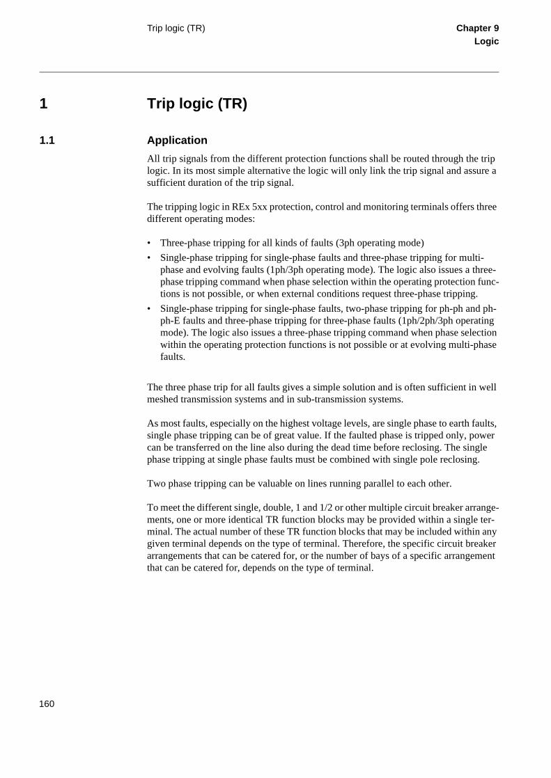
Trip logic (TR) Chapter 9Logic
i-hree- func-.
ph-ting ection ase
well
faults, wer gle .
nge-ter- any aker ement
1 Trip logic (TR)
1.1 Application
All trip signals from the different protection functions shall be routed through the trip logic. In its most simple alternative the logic will only link the trip signal and assure a sufficient duration of the trip signal.
The tripping logic in REx 5xx protection, control and monitoring terminals offers three different operating modes:
• Three-phase tripping for all kinds of faults (3ph operating mode)
• Single-phase tripping for single-phase faults and three-phase tripping for multphase and evolving faults (1ph/3ph operating mode). The logic also issues a tphase tripping command when phase selection within the operating protectiontions is not possible, or when external conditions request three-phase tripping
• Single-phase tripping for single-phase faults, two-phase tripping for ph-ph andph-E faults and three-phase tripping for three-phase faults (1ph/2ph/3ph operamode). The logic also issues a three-phase tripping command when phase selwithin the operating protection functions is not possible or at evolving multi-phfaults.
The three phase trip for all faults gives a simple solution and is often sufficient in meshed transmission systems and in sub-transmission systems.
As most faults, especially on the highest voltage levels, are single phase to earth single phase tripping can be of great value. If the faulted phase is tripped only, pocan be transferred on the line also during the dead time before reclosing. The sinphase tripping at single phase faults must be combined with single pole reclosing
Two phase tripping can be valuable on lines running parallel to each other.
To meet the different single, double, 1 and 1/2 or other multiple circuit breaker arraments, one or more identical TR function blocks may be provided within a single minal. The actual number of these TR function blocks that may be included withingiven terminal depends on the type of terminal. Therefore, the specific circuit brearrangements that can be catered for, or the number of bays of a specific arrangthat can be catered for, depends on the type of terminal.
160
Trip logic (TR) Chapter 9Logic
for tions
seg-ts en- not of the
ercur-e for uni-
ver-ese
to one rmi- pole, e
for pro-ole.
One TR function block should be used for each breaker, if the line is connected to the substation via more than one breaker. Assume that single pole tripping and auto-reclos-ing is used for the line. The breaker chosen as master must in that case have single pole tripping, while the slave breaker could have three pole tripping and auto-reclosing. In case of a permanent fault only one of the breakers has to be operated at the second en-ergising of the fault. In case of a transient fault the slave breaker reclosing is made as a three pole reclosing onto the non-faulted line.
The same philosophy can be used for two-pole tripping and auto-reclosing.
1.2 Functionality
The minimum duration of a trip output signal from the TR function is 150ms. This is to secure the fault clearance.
The three-pole TR function has a single input through which all trip output signals from the protection functions within the terminal, or from external protection functions via one or more of the terminal’s binary inputs, are routed. It has a single trip output connection to one or more of the terminal’s binary outputs, as well as to other funcwithin the terminal requiring this signal.
The expanded TR function for single- and two-pole tripping has additional phaseregated inputs for this, as well as inputs for faulted phase selection. The latter inpuable single- and two-pole tripping for those functions which do not have their ownphase selection capability, and therefore which have just a single trip output and phase segregated trip outputs for routing through the phase segregated trip inputsexpanded TR function. Examples of such protection functions are the residual ovrent protections. The expanded TR function has two inputs for these functions, onimpedance tripping (e.g. carrier-aided tripping commands from the scheme commcation logic), and one for earth fault tripping (e.g. tripping output from a residual ocurrent protection). Additional logic secures a three-pole final trip command for thprotection functions in the absence of the required phase selection signals.
The expanded TR function has three trip outputs, one per phase, for connection or more of the terminal’s binary outputs, as well as to other functions within the tenal requiring these signals. There are also separate output signals indicating singletwo pole or three pole trip. These signals are important for the cooperation with thauto-reclosing function.
The expanded TR function is equipped with logic which secures correct operationevolving faults as well as for reclosing on to persistent faults. A special input is alsovided which disables single- and two-pole tripping, forcing all tripping to be three-p
161

Trip logic (TR) Chapter 9Logic
e
h or
on
on
ions
in-
se
In case of multi-breaker arrangement, one TR function block can be used for each breaker, if the breaker functions differ. This can be the case if single pole trip and auto-reclosing is used.
1.3 Design
The function consists of the following basic logic parts:
• A three-phase front logic that is activated when the terminal is set into exclusivthree-phase operating mode.
• A phase segregated front logic that is activated when the terminal is in 1ph/3p1ph/2ph/3ph operating mode.
• An additional logic for evolving faults and three-phase tripping when the functioperates in 1ph/3ph operating mode.
• An additional logic for evolving faults and three-phase tripping when the functioperates in 1ph/2ph/3ph operating mode.
• The final tripping circuits.
Three-phase front logic
Figure 66 shows a simplified block diagram of a three-phase front logic. Descriptof different signals are available in signal list.
Figure 66: Three-phase front logic - simplified logic diagram
Any of active functional input signals activates the RSTTRIP internal signal, whichfluences the operation of the final tripping circuits.
Phase segregated front logic
The following input signals to the single-phase front logic influence the single-phatripping of the terminal (see figure 67):
99000456.vsd
TRIP-TRINL1
TRIP-TRINL2
TRIP-TRINL3
TRIP-1PTRZ
TRIP-1PTREF
TRIP-TRIN
>1
>1
>1
Program = 3ph
& RSTTRIP - cont.
162

Trip logic (TR) Chapter 9Logic
an signals nal
ns gen- the
func-
trip-ich
n ith e
• Phase related tripping signals from different built-in protection functions that coperate on a phase segregated basis and are used in the terminal. The outputof these functions should be configured to the TRIP-TRINLn (n = 1...3) functioinputs.
• Internal phase-selective tripping signals from different phase selection functiowithin the terminal, like PHS (phase selection for distance protection) or GFC (eral fault criteria). The output signals of these functions should be configured toTRIP-PSLn (n = 1...3) functional inputs. It is also possible to connect to these tional inputs different external phase selection signals.
• Single-phase tripping commands from line distance protection or carrier aidedping commands from scheme communication logic for distance protection, whinitiate single-phase tripping. These signals should be configured to the TRIP-1PTRZ functional input. It is also possible to configure a tripping output from aearth-fault overcurrent protection, to initiate the single-pole trip in connection wsome external phase selection function. This signal should be configured to thTRIP-1PTREF functional input.
Figure 67: Phase segregated front logic
99000457.vsd
TRIP-TRINL1
TRIP-PSL1
TRIP-TRINL2
TRIP-PSL2
TRIP-TRINL3
TRIP-PSL3
TRIP-1PTREF
TRIP-1PTRZ
-loop-loop
TRIP-TRIN
L1TRIP - cont.
L2TRIP - cont.
L3TRIP - cont.
>1
>1
>1
&
&
&
>1
>1
>1
&
>1
&
>1
&&
t
50 ms
163

Trip logic (TR) Chapter 9Logic
The TRIP-1PTRZ signal enables tripping corresponding to phase selection signals without any restriction while any phase selective external tripping signals prevent such tripping from the TRIP-1PTREF signal.
If any of these signals continues for more than 50 ms without the presence of any phase selection signals, three-phase tripping command is issued.
It is possible to configure the TRIP-1PTREF signal to the output signal of the EF---TRIP overcurrent, earth-fault, protection function (directional and nondirectional). This enables single-phase tripping when the faulty phase is detected by some other phase-selection element such as the phase selection in distance protection.
Additional logic for 1ph/3ph operating mode
Figure 68 presents the additional logic when the trip function is in 1ph/3ph operating mode. A TRIP-P3PTR functional input signal activates a three pole tripping if at least one phase within the front logic initiates a trip command.
164
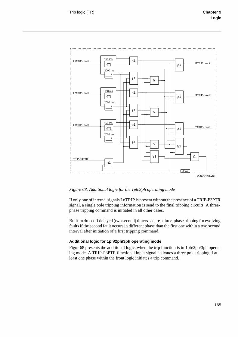
Trip logic (TR) Chapter 9Logic
Figure 68: Additional logic for the 1ph/3ph operating mode
If only one of internal signals LnTRIP is present without the presence of a TRIP-P3PTR signal, a single pole tripping information is send to the final tripping circuits. A three-phase tripping command is initiated in all other cases.
Built-in drop-off delayed (two second) timers secure a three-phase tripping for evolving faults if the second fault occurs in different phase than the first one within a two second interval after initiation of a first tripping command.
Additional logic for 1ph/2ph/3ph operating mode
Figur 68 presents the additional logic, when the trip function is in 1ph/2ph/3ph operat-ing mode. A TRIP-P3PTR functional input signal activates a three pole tripping if at least one phase within the front logic initiates a trip command.
99000458.vsd
L1TRIP - cont.
L2TRIP - cont.
L3TRIP - cont.
TRIP-P3PTR
-loop
RTRIP - cont.
STRIP - cont.
TTRIP - cont.
150 ms
t>1
t
2000 ms
>1&
>1
>1
150 ms
t>1
t
2000 ms
>1&
>1
>1
&
>1150 ms
t
t
2000 ms
>1&
>1
>1
165
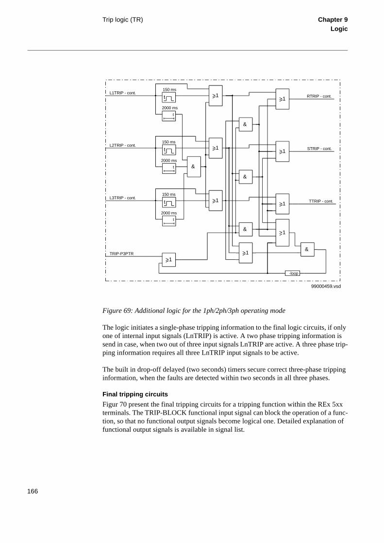
Trip logic (TR) Chapter 9Logic
Figure 69: Additional logic for the 1ph/2ph/3ph operating mode
The logic initiates a single-phase tripping information to the final logic circuits, if only one of internal input signals (LnTRIP) is active. A two phase tripping information is send in case, when two out of three input signals LnTRIP are active. A three phase trip-ping information requires all three LnTRIP input signals to be active.
The built in drop-off delayed (two seconds) timers secure correct three-phase tripping information, when the faults are detected within two seconds in all three phases.
Final tripping circuits
Figur 70 present the final tripping circuits for a tripping function within the REx 5xx terminals. The TRIP-BLOCK functional input signal can block the operation of a func-tion, so that no functional output signals become logical one. Detailed explanation of functional output signals is available in signal list.
99000459.vsd
L1TRIP - cont.150 ms
t
t
2000 ms
L2TRIP - cont.
L3TRIP - cont.
TRIP-P3PTR
-loop
RTRIP - cont.
STRIP - cont.
TTRIP - cont.
&
>1
>1
>1
>1
&>1
>1
t
2000 ms
150 ms
t
t
2000 ms
150 ms
t
&
&
&
>1
>1
>1
166

Trip logic (TR) Chapter 9Logic
Figure 70: Final tripping circuits
99000555.vsd
TRIP-BLOCK
RTRIP -cont.
>1
>1
>1
STRIP - cont.
TTRIP -cont.
RSTTRIP -cont.
&
&
&
>1
&>1
&
-loop
&
&
&>1
&
-loop
& t
10 ms
t
5 msTRIP-TR2P
TRIP-TR1P
TRIP-TR3P
TRIP-TRL1
TRIP-TRL2
TRIP-TRL3
TRIP-TRIP
167
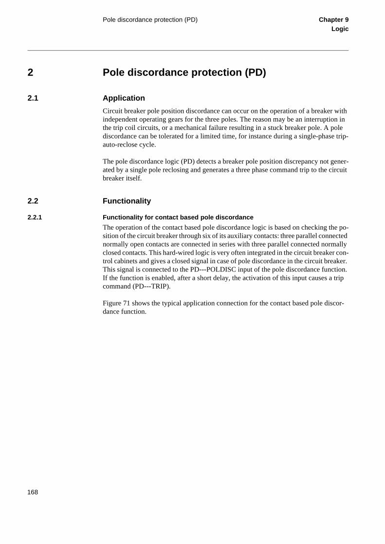
Pole discordance protection (PD) Chapter 9Logic
2 Pole discordance protection (PD)
2.1 Application
Circuit breaker pole position discordance can occur on the operation of a breaker with independent operating gears for the three poles. The reason may be an interruption in the trip coil circuits, or a mechanical failure resulting in a stuck breaker pole. A pole discordance can be tolerated for a limited time, for instance during a single-phase trip-auto-reclose cycle.
The pole discordance logic (PD) detects a breaker pole position discrepancy not gener-ated by a single pole reclosing and generates a three phase command trip to the circuit breaker itself.
2.2 Functionality
2.2.1 Functionality for contact based pole discordance
The operation of the contact based pole discordance logic is based on checking the po-sition of the circuit breaker through six of its auxiliary contacts: three parallel connected normally open contacts are connected in series with three parallel connected normally closed contacts. This hard-wired logic is very often integrated in the circuit breaker con-trol cabinets and gives a closed signal in case of pole discordance in the circuit breaker. This signal is connected to the PD---POLDISC input of the pole discordance function. If the function is enabled, after a short delay, the activation of this input causes a trip command (PD---TRIP).
Figure 71 shows the typical application connection for the contact based pole discor-dance function.
168
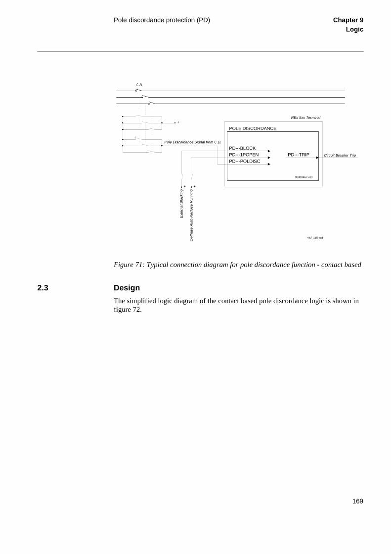
Pole discordance protection (PD) Chapter 9Logic
Figure 71: Typical connection diagram for pole discordance function - contact based
2.3 Design
The simplified logic diagram of the contact based pole discordance logic is shown in figure 72.
Ext
erna
l Blo
ckin
g
1-P
hase
Aut
o R
eclo
se R
unni
ng
visf_115.vsd
Circuit Breaker Trip
++
Pole Discordance Signal from C.B.
+
C.B.
REx 5xx Terminal
PD---BLOCKPD---1POPENPD---POLDISC
PD---TRIP
POLE DISCORDANCE
99000467.vsd
169
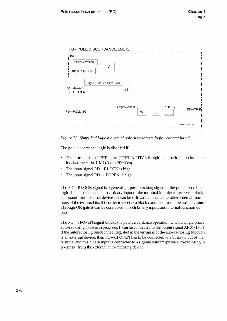
Pole discordance protection (PD) Chapter 9Logic
een
nce ock nc-ns.
out-
hase 1PT1 tion f the ng in
Figure 72: Simplified logic digram of pole discordance logic - contact based
The pole discordance logic is disabled if:
• The terminal is in TEST status (TEST-ACTIVE is high) and the function has bblocked from the HMI (BlockPD=Yes)
• The input signal PD---BLOCK is high
• The input signal PD---1POPEN is high
The PD---BLOCK signal is a general purpose blocking signal of the pole discordalogic. It can be connected to a binary input of the terminal in order to receive a blcommand from external devices or can be software connected to other internal futions of the terminal itself in order to receive a block command from internal functioThrough OR gate it can be connected to both binary inputs and internal function puts.
The PD---1POPEN signal blocks the pole discordance operation when a single pauto-reclosing cycle is in progress. It can be connected to the output signal AR01-if the autoreclosing function is integrated in the terminal; if the auto-reclosing funcis an external device, then PD---1POPEN has to be connected to a binary input oterminal and this binary input is connected to a signallisation “1phase auto-reclosiprogress” from the external auto-reclosing device.
PD---BLOCKPD---1POPEN
PD---POLDISCPD---TRIP
99000468.vsd
t
t 150 ms&
Logic Enable
PD - POLE DISCORDANCE LOGIC
>1
TEST-ACTIVE
&
TEST
BlockPD = Yes
Logic Blocked form Test
170
Pole discordance protection (PD) Chapter 9Logic
If one or two poles of the circuit breaker have failed to open or to close (pole discor-dance status), then the function input PD---POLDISC is activated from the pole discor-dance signal derived from the circuit breaker auxiliary contacts (one NO contact for each phase connected in parallel, and in series with one NC contact for each phase con-nected in parallel). If the pole discordance function is enabled, a 150 ms trip pulse com-mand (PD---TRIP) is generated, after a settable time interval t (0-60 s).
2.4 Calculations
2.4.1 Setting Instruction
The setting parameters are accessible through the HMI. The parameters for the pole dis-cordance logic are found in the HMI-tree under:
Setting
Functions
Group 1,2,3 and 4
PoleDiscord
The parameters and their setting ranges are shown in the appendix.
Comments regarding settings:
Operation: Pole discordance protection On/Off. Activation or de-activation of
the logic.
Time delay , t: The time delay is not critical because the pole discordance logic operates mainly with load conditions. The time delay should be
chosen between 0.5 and 1 s.
171
Communication channel logic (CCHL) Chapter 9Logic
king from
n. It nt in-
ined
failed d in both l-out-
-two logic is in-
that
3 Communication channel logic (CCHL)
3.1 Application
The security of the protection system can be influenced by the performance of commu-nication channels. In many applications spurious signals or absence of signals can cause malfunction of the protection system. One example is when direct intertrip is used where a false signal will cause unwanted tripping.
In order to increase security double communication channels between the line ends can be used. For the combination of two channels the communication channel logic (CCHL) is used. CCHL is intended to be used together with the system protection and control functions. This logic combines the two received signals to one CR signal in the terminal. The logic will accept the two channel signals as simultaneous only if they ap-pear both during a settable time. Further the logic detects faults in the communication channels and blocks or changes the decision mode from two-channel-out-of-two into one-channel-out-of-two.
In case of a “dead” communication channel there is a possibility to have an unblocfunction activated. If there is no CR signal, no CGuard signal and no fault signal the PLC equipment, this can be transferred to a CR signal in the terminal.
3.2 Functionality
General
CCHL is used together with different sub-functions of a system protection functiohas an independent function block with two independent channels (four independeput channels). Their cooperation with different measuring functions will be determby means of a terminal configuration tools (CAP 531, for example).
The CCHL logic receives channel received, channel guard received and channel signals from both communication channels. The unblocking logic is not incorporatethe logic for the receipt of both channels. To have this output, the actual signals forchannels must be simultaneously received. The logic for the receipt of one-channeof-two is enabled by way of an input signal. Furthermore, the one-channel-out-ofoutput can only be given if one of the communications channels has failed, as thisis supervised by the failure of either channel. When selected, the unblocking logiccorporated within this one-out-of-two logic.
The CCHL logic incorporates a number of security timers to make absolutely sureno erroneous outputs are given for spurious channel received signals.
172
Communication channel logic (CCHL) Chapter 9Logic
The CCHL logic also provides, for each channel, a communications channel failed out-put.
Basic signals from each communication channel
Each communication channel has three basic output signals, which are used as inputs to the logic:
- CRn (n is a serial number of communication channel) is an input signal on received carrier signal, see figure 73.
- CRGn is a guard signal for the corresponding communication channel. It is normal, that this signal is logical one, when CRn is logical zero and vice-versa. The input should be configured to FIXD-OFF, if the CRGn signal is not available from the carrier com-munication equipment.
- COMFn is an input signal, which informs on the operation of a self-supervision func-tion within the carrier communication equipment used. The input should be configured to FIXD-OFF, if the signal is not available on the communication equipment.
Figure 73: Communication channel logic 1
Time delayed operation for one only received communication signal
If one communication channel has been detected as faulty (see section ) and the operat-ing mode has been permitted to change from two-of-two to one-of-two, a CCHL-CR appears after a time delay, set on tSec1 timer in case, that the second channel is healthy and the CRn signal appears without the presence of a CRGn signal.
CCHL-CR1
&CCHL-CRG1 t
tSec1
CCHL-COMF1
Unblock1=On
CCHL-CRL1CH
>1
>1Unblocking logic
en01000033.vsd
1
173
Communication channel logic (CCHL) Chapter 9Logic
Unblocking logic within each separate signal
For an illustration of an unblocking logic within each separate signal, see figure 73. If none of signals CCHL-CR1 and CCHL-CRG1 is present for a time longer than the one set on a tSec1 timer and no CCHL-COMF1 signal has been detected, an unblocking log-ic for a particular signal channel is permitted to operate. The operation of this logic is additionally conditioned by the Unblockn setting parameter, which must be set to Un-blockn = On, if the logic is intended to operate. The logic is practically the same as used together with the communication logic for the line distance protection (ZCOM func-tion). The difference is that the tReSt restart timer and the tSig signal timer are settable.
Simultaneous presence of two carrier receive signals
For an illustration of a simultaneous presence of two carrier receive signals, see figure 74. If both carrier receive signals (CCHL-CR1 and CCHL-CR2) are present at the same moment and both guard signals go to logical zero, the output signals CCHL-CR goes high after a time delay, which is settable on the security timer TSecC. The most com-mon setting for this timer is 0 ms, because the high enough security is obtained already with serial connection of two communication channels. This mode of operation is also indicated by the appearance of CCHL-CRL2CH output signal.
Figure 74: Combination of two communication channels
Detection of a failed communication channel
For an illustration of a combination of two communication channels, see figure 75. The communication channel is understood as faulty under the following conditions:
- If CR1 and CRG1 signals are present simultaneously for more than 20 ms and no COMF1 signal has been present
- If a COMF1 signal appears on the corresponding functional input
- If non of the three input signals (CR1, CRG1, and COMF1) appears for more than the time delay set on a security timer tSec2.
The logic detects the faulty channel and sets high the corresponding CCHL-CH1FAIL output signal.
C C H L -C R 1
&C C H L -C R G 1
C C H L -C R 2
&C C H L -C R G 2
& ttS e c C
C C H L -C R L 2 C H
e n 0 1 0 0 0 0 3 4 .v s d
174

Communication channel logic (CCHL) Chapter 9Logic
In all three cases the logic checks also the CCHL-2TO1OK input signal, which is com-mon to both communication channels. This signal determines whether it is possible to switch the operating mode from two-of-two to one-of-two or not. This means that the user can influence this change by configuring the CCHL-2TO1OK to FIXD-ON (change permitted) or to FIXD-OFF (switch not permitted).
The CCHL-CRL1CH output signal goes high, if a fault has been detected on one com-munication channel and the second communication channel has operated correctly and transmitted the corresponding carrier signal.
Figure 75: communication channel fail logic.
3.3 Calculations
There are some time settings to be made:
tSecC: the time for which the signals from both channels must be simultaneous received before a CR signal is given as an output from the logic. In most cases this timer can be set to 0.
tSec1: Security time to ensure definite, and not spurious, receipte of the channel signal. This time delay shall be about the same as the shortest puls time of the CS signal from the remote line end.
tSec2: Security time following the loss of guard signal before activation of the unblock-ing logic. The setting shall be longer than the possible time difference between the change of CR and CRG signals. 50 ms is recommended.
C C H L -C R 1
C C H L -C R G 1
C C H L -C O M F 1
& > 1 C C H L -C H 1 F A ILt
2 0 m s
ttS e c 2
> 1
e n 0 1 0 0 0 0 3 5 .v s d
175

Communication channel test logic (CCHT)
Chapter 9Logic
4 Communication channel test logic (CCHT)
4.1 Application
Many applications in secondary systems require testing of different functions with con-firmed information on successfully completed test. Carrier channel test (CCHT) func-tion serves primarily testing of communication (power line carrier) channels in applications, where continuous monitoring by some other means is not possible due to technical or economical reasons.
The logic initiates sending of some impulse (carrier send signal), which starts the oper-ation of different functions outside the logic, and checks the feedback from the external function. It reports the successful or non-successful response on initiated test. It is also possible to abort the test with some external signal, which overrules all internal process.
It is possible to initiate the logic manually or automatically. Manual starts are possible by means of external push-button, connected to the binary input of a terminal. Automat-ic starts are possible in long time intervals with their duration dependent on setting of the corresponding timer.
4.2 Design
Figure 76 presents a simplified logic diagram for the CCHT function. Logical one on CCHT-BLOCK functional input disables completely the operation of the logic.
176

Communication channel test logic (CCHT)
Chapter 9Logic
” re-f log-the
the
et on n as
tWait be-ce of dis-
Figure 76: Simplified logic diagram for the CCHT function
Selection of an operating mode
Selection of an operating mode, which determines the automatic (internal) or manual (external) start is possible by setting the “Operation = Aut” and “Operation = Manspectively (see figure 76). The automatic starting requires continuous presence oical one on CCHT-START functional input. Setting of the tStart timer determines time intervals for the automatic starts logic.
Any presence of the logical one signal on the CCHT-START functional input startsfunction, when in manual operating mode.
Operation at sending end
Manual or automatic start initiates the pulse, which is 15 ms longer than the time sa tWait timer. This pulse initiates the CCHT-CS functional output signal in duratioset on a tCS pulse timer.The same pulse starts also the time measurement by thetimer. The CCHT-ALARM output signal appears, if the CCHT-CR input does not come logical one within the time interval, as set on the tWait timer. The appearanthe CCHT-CR signal is safeguarded by a 15 ms timer, to prevent influence of theturbances on a communication link.
CCHT-BLOCK
Operation=Man
&CCHT-START
&Operation=Aut t
tStart>1
-loop
ttCh
t15 ms
&
CCHT-CR t
15 ms
>1
t
tWait
&
&
&CCHT-RESET >1
&>1
&
CCHT-CHOK
CCHT-ALARM
CCHT-CS
99000187.vsd
&
&tCS
t
tChOK
t
tWait
t
177
Communication channel test logic (CCHT)
Chapter 9Logic
The appearance of the CCHT-CR signal within the tWait time interval activates the CCHT-CHOK output signal. It remains active for the period as set on the timer tChOK or until the CCHT-ALARM appears at new start of a CCHT function.
The tCh timer, which is delayed on drop-off, prevents ringing of a complete system. It is possible to reset the CCHT-ALARM output signal by activating the CCHT-RESET functional input.
Operation at receiving end
Activation of a CCHT-CR functional input activates instantaneously the CCHT-CS functional output, if the timer tCh has not been activated or the function has not been blocked by the active CCHT-BLOCK functional input. Duration of the CCHT-CR in-put signal must be longer than 15 ms to avoid operation at different disturbances on communication link.
178
Event function (EV) Chapter 9Logic
5 Event function (EV)
5.1 Application
When using a Substation Automation system, events can be spontaneously sent or polled from the terminal to the station level. These events are created from any available signal in the terminal that is connected to the event function block. The event function block can also handle double indication, that is normally used to indicate positions of high-voltage apparatuses. With this event function block, data also can be sent to other terminals over the interbay bus.
5.2 Functionality
The events can be created from both internal logical signals and binary input channels. The internal signals are time tagged in the main processing module, while the binary input channels are time tagged directly on each I/O module. The events are produced according to the set event masks. The event masks are treated commonly for both the LON and SPA channels. All events according to the event mask are stored in a buffer, which contains up to 1000 events. If new events appear before the oldest event in the buffer is read, the oldest event is overwritten and an overflow alarm appears.
The outputs from the event function block are formed by the reading of status and events by the station HMI on either every single input or double input. The user-defined name for each input is intended to be used by the station HMI.
Twelve of the event function blocks are executed with fast cyclicity. That means that the time-tagging resolution on the events that are emerging from internal logical sig-nals, created from configurable logic, is the same as the cyclicity of this logic. The time tagging resolution on the events that are emerging from binary input signals have a res-olution of 1 ms.
Two special signals for event registration purposes are available in the terminal, Termi-nal restarted and Event buffer overflow.
5.3 Design
General
As basic, 12 event function blocks EV01-EV12 running with a fast cyclicity, are avail-able in REx 5xx. When the function Apparatus control is included in the terminal, ad-ditional 32 event function blocks EV13-EV44, running with a slower cyclicity, are available.
179

Event function (EV) Chapter 9Logic
ich
unc-ndard
xam-scon-n the e the tes.
nder
on the
Each event function block has 16 connectables corresponding to 16 inputs INPUT1 to INPUT16. Every input can be given a name with up to 19 characters from the CAP 531 configuration tool.
The inputs can be used as individual events or can be defined as double indication events.
The inputs can be set individually from the Parameter Setting Tool (PST) under the Mask-Event function as:
• No events
• OnSet, at pick-up of the signal
• OnReset, at drop-out of the signal
• OnChange, at both pick-up and drop-out of the signal
Also an input PrColxx (xx=01-44) is available on the function block to define on whprotocol the events shall be sent.
The event function blocks EV01-EV06 have inputs for information numbers and ftion type, which are used to define the events according to the communication staIEC 60870-5-103.
Double indication
Double indications are used to handle a combination of two inputs at a time, for eple, one input for the open and one for the close position of a circuit breaker or dinector. The double indication consists of an odd and an even input number. Wheodd input is defined as a double indication, the next even input is considered to bother input. The odd inputs has a suppression timer to suppress events at 00 sta
To be used as double indications the odd inputs are individually set from the SMS uthe Mask-Event function as:
• Double indication
• Double indication with midposition suppression
Here, the settings of the corresponding even inputs have no meaning.
These states of the inputs generate events. The status is read by the station HMIstatus indication for the odd input:
180

Event function (EV) Chapter 9Logic
d to send nsfer nt sed
r-
- via ckup ta, e N the .
d as
e set-
the
• 00 generates an intermediate event with the read status 0
• 01 generates a close event with the read status 1
• 10 generates an open event with the read status 2
• 11 generates an undefined event with the read status 3
Communication between terminals
The BOUND and INTERVAL inputs are available on the event function block.
The BOUND input set to 1 means that the output value of the event block is bounanother control terminal on the LON bus. The event function block is then used to data over the LON bus to other REx 5xx terminals. The most common use is to trainterlocking information between different bays. That can be performed by an evefunction block used as a send block and with a Multiple Command function block uas a receive block. The document Apparatus Control describes how to transfer the in-terlocking information. The configuration of the communication between control teminals is made by the LON Network Tool.
The INTERVAL input is applicable only when the BOUND input is set to 1. The INTERVAL is intended to be used for cyclic sending of data to other control terminalsthe LON bus with the interval time as set. This cyclic sending of data is used as a baof the event-driven sending, which always is performed. With cyclic sending of dathe communication can be supervised by a corresponding INTERVAL input on thMultiple Command function block in another control terminal connected to the LObus. This INTERVAL input time is set a little bit longer than the interval time set on event function block. With INTERVAL=0, only event-driven sending is performed
5.4 Calculations
The event reporting can be set from the PST as:
• Use event masks
• Report no events
• Report all events
Use of event masks is the normal reporting of events, that is, the events are reportedefined in the database.
An event mask can be set individually for each available signal in the terminal. Thting of the event mask can only be performed from the PST.
All event mask settings are treated commonly for all communication channels of terminal.
181
Event function (EV) Chapter 9Logic
bus.
C
d-
D pa-
Report no events means blocking of all events in the terminal.
Report all events means that all events, that are set to OnSet/OnReset/OnChange are re-ported as OnChange, that is, both at set and reset of the signal. For double indications when the suppression time is set, the event ignores the timer and is reported directly. Masked events are still masked.
Parameters to be set for the event function block are:
• T_SUPRyy including the suppression time for double indications.
• NAMEyy including the name for each input.
• PrColxx including the type of protocol for sending the events.
• INTERVAL used for the cyclic sending of data.
• BOUND telling that the block has connections to other terminals over the LON
• FuncTEVx (for EV01-EV06) including the function type for sending events via IE60870-5-103.
• InfoNoyy (for EV01-EV06) including the information number for the events sening via IEC 60870-5-103.
These parameters are set from the CAP 531 configuration tool. When the BOUNrameter is set, the settings of the event masks have no meaning.
182
Event counter (CN) Chapter 9Logic
6 Event counter (CN)
6.1 Application
The function consists of six counters which are used for storing the number of times each counter has been activated. It is also provided with a common blocking function for all six counters, to be used for example at testing. Every counter can separately be set on or off by a parameter setting.
6.2 Functionality
The function block has six inputs for increasing the counter values for each of the six counters respectively. The content of the counters are stepped one step for each positive edge of the input respectively. The maximum count up speed is 10 pulses per second. The maximum counter value is 10 000. For counts above 10 000 the counter will stop at 10 000 and no restart will take place. At power interrupt the counter values are stored.
The function block also has an input BLOCK. At activation of this input all six counters are blocked. The input can for example be used for blocking the counters at testing.
All inputs are configured via configuration tool CAP 531.
Reporting
The content of the counters can be read in the local HMI under the menu:
ServiceReport
Functions
Counters
Count
Counters
Reset of counters can be performed in the local HMI under the menu:
183

Event counter (CN) Chapter 9Logic
ServiceReport
Functions
Counters
Count
ClearCounters
Reading of content and resetting of the counters can also be performed remotely, for example via SPA-communication.
6.3 Calculations
The parameters for the counters, Operation = Off/On, are set in the local HMI under the menu:
Settings
Functions
Group n
Counters
or via the PST Parameter Setting Tool.
184

About this chapter Chapter 10Monitoring
Chapter 10 Monitoring
About this chapter
This chapter describes the monitoring functions.
185
LED indication function (HL, HLED) Chapter 10Monitoring
ls ap-en re-
eer status ly or
two used et cting
If t pri-
ly un-sed
1 LED indication function (HL, HLED)
1.1 Application
The LED indication module is an additional feature for the REx 500 terminals for pro-tection and control and consists totally of 18 LEDs (Light Emitting Diodes). It is located on the front of the protection and control terminal. The main purpose is, to present on site an immediate visual information on:
• actual signals active (or not active) within the protected bay (terminal).
• alarm signals handled as a simplified alarm system.
• last operation of the terminal. Here we understand the presentation of the signapeared during the latest start(s) or trip(s) since the previous information has beset.
The user of this information is the technician in substation or the protection enginduring the testing activities. The protection engineer can also be able to read the of all LEDs over the SMS in his office as well as to acknowledge/reset them localremotely.
1.2 Functionality
Each LED indication can be set individually to operate in six different sequences;as follow type and four as latch type. Two of the latching types are intended to beas a protection indication system, either in collecting or re-starting mode, with resfunctionality. The other two are intended to be used as a signaling system in collemode with an acknowledgment functionality.
Priority
Each LED can show green, yellow or red light, each with its own activation input.more than one input is activated at the time a priority is used with green as lowesority and red as the highest.
Operating modes
Collecting mode
LEDs which are used in collecting mode of operation are accumulated continuoustil the unit is acknowledged manually. This mode is suitable when the LEDs are uas a simplified alarm system.
186
LED indication function (HL, HLED) Chapter 10Monitoring
Re-starting mode
In the re-starting mode of operation each new start resets all previous active LEDs and activates only those which appear during one disturbance. Only LEDs defined for re-starting mode with the latched sequence type 6 (LatchedReset-S) will initiate a reset and a restart at a new disturbance. A disturbance is defined to end a settable time after the reset of the activated input signals or when the maximum time limit has been elapsed.
Acknowledgment/reset
From local HMI
The active indications can be acknowledged/reset manually. Manual acknowledgment and manual reset have the same meaning and is a common signal for all the operating sequences and LEDs. The function is positive edge triggered, not level triggered. The acknowledgment/reset is performed via the C-button on the Local HMI according to the sequence in figure 77.
187

LED indication function (HL, HLED) Chapter 10Monitoring
Figure 77: Acknowledgment/reset from local HMI
From function input
The active indications can also be acknowledged/reset from an input (ACK_RST) to the function. This input can for example be configured to a binary input operated from an external push button. The function is positive edge triggered, not level triggered. This means that even if the button is continuously pressed, the acknowledgment/reset only affects indications active at the moment when the button is first pressed.
From SMS/SCS
It is also possible to perform the acknowledgment/reset remotely from SMS/SCS. To do that, the function input (ACK_RST) has to be configured to an output of a command function block (CD or CM). The output from these command function blocks can then be activated from the SMS/SCS.
en01000226.vsd
Darkscreen
Screen scrollingdisturbanceindications
EC C
Text on HMI:C=Clear LEDsE=Enter menu
C E
Clear HMI-LCD LEDs Go to menu
If any HMI-LEDs active, text on HMI:C=HLED_ ACK_RSTE=Enter menu
C E
Acknowledge/ResetHMI-LEDs
Go to menu
Press button:
188
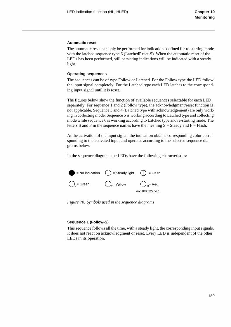
LED indication function (HL, HLED) Chapter 10Monitoring
Automatic reset
The automatic reset can only be performed for indications defined for re-starting mode with the latched sequence type 6 (LatchedReset-S). When the automatic reset of the LEDs has been performed, still persisting indications will be indicated with a steady light.
Operating sequences
The sequences can be of type Follow or Latched. For the Follow type the LED follow the input signal completely. For the Latched type each LED latches to the correspond-ing input signal until it is reset.
The figures below show the function of available sequences selectable for each LED separately. For sequence 1 and 2 (Follow type), the acknowledgment/reset function is not applicable. Sequence 3 and 4 (Latched type with acknowledgement) are only work-ing in collecting mode. Sequence 5 is working according to Latched type and collecting mode while sequence 6 is working according to Latched type and re-starting mode. The letters S and F in the sequence names have the meaning S = Steady and F = Flash.
At the activation of the input signal, the indication obtains corresponding color corre-sponding to the activated input and operates according to the selected sequence dia-grams below.
In the sequence diagrams the LEDs have the following characteristics:
Figure 78: Symbols used in the sequence diagrams
Sequence 1 (Follow-S)
This sequence follows all the time, with a steady light, the corresponding input signals. It does not react on acknowledgment or reset. Every LED is independent of the other LEDs in its operation.
= No indication = Steady light = Flash
en01000227.vsd
G= GreenY= Yellow R= Red
189
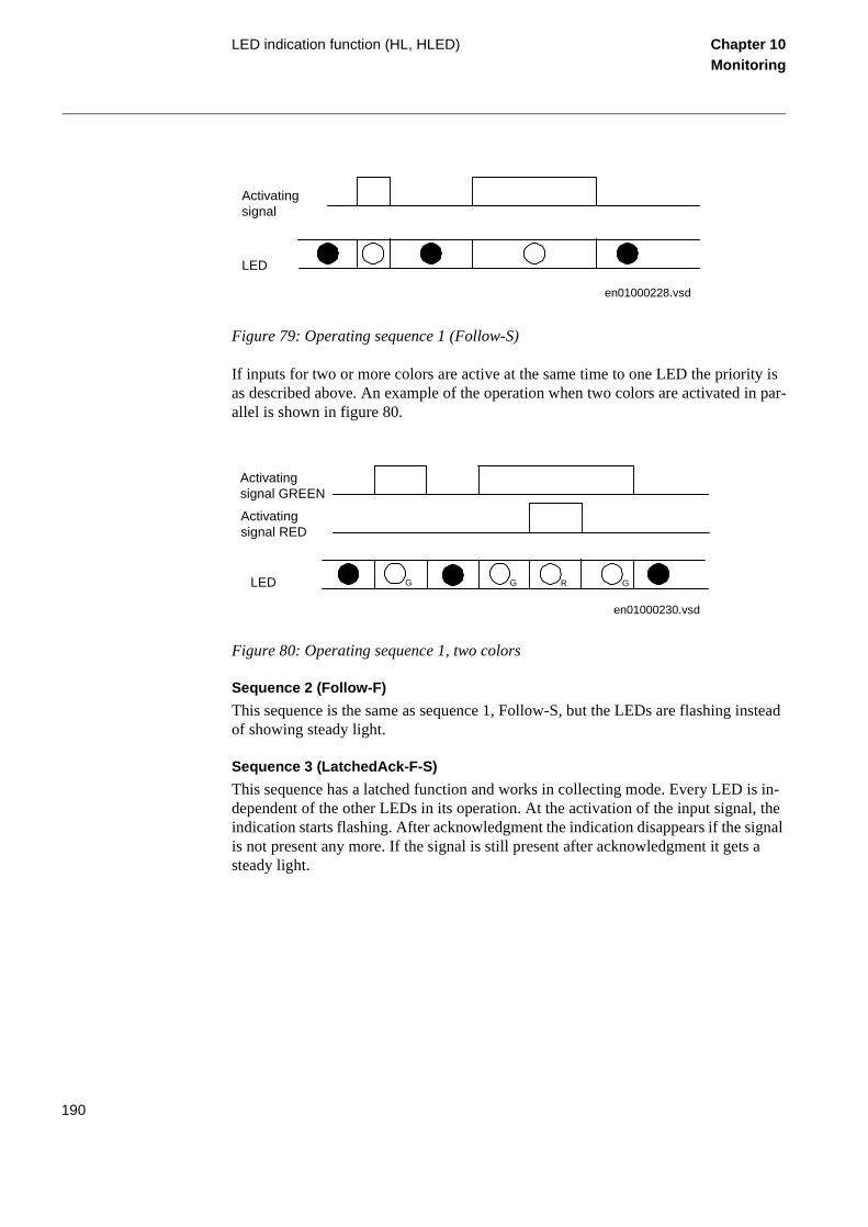
LED indication function (HL, HLED) Chapter 10Monitoring
Figure 79: Operating sequence 1 (Follow-S)
If inputs for two or more colors are active at the same time to one LED the priority is as described above. An example of the operation when two colors are activated in par-allel is shown in figure 80.
Figure 80: Operating sequence 1, two colors
Sequence 2 (Follow-F)
This sequence is the same as sequence 1, Follow-S, but the LEDs are flashing instead of showing steady light.
Sequence 3 (LatchedAck-F-S)
This sequence has a latched function and works in collecting mode. Every LED is in-dependent of the other LEDs in its operation. At the activation of the input signal, the indication starts flashing. After acknowledgment the indication disappears if the signal is not present any more. If the signal is still present after acknowledgment it gets a steady light.
Activatingsignal
LED
en01000228.vsd
Activatingsignal GREEN
LED
en01000230.vsd
G R GG
Activatingsignal RED
190

LED indication function (HL, HLED) Chapter 10Monitoring
Figure 81: Operating sequence 3 (LatchedAck-F-S)
When an acknowledgment is performed, all indications that appear before the indica-tion with higher priority has been reset, will be acknowledged, independent of if the low priority indication appeared before or after acknowledgment. In figure 82 is shown the sequence when a signal of lower priority becomes activated after acknowledgment has been performed on a higher priority signal. The low priority signal will be shown as ac-knowledged when the high priority signal resets.
Figure 82: Operating sequence 3, two colors involved
If all three signals are activated the order of priority is still maintained. Acknowledg-ment of indications with higher priority will acknowledge also low priority indications which are not visible according to figure 83.
Activatingsignal
LED
Acknow.en01000231.vsd
Activatingsignal RED
LED
Acknow.en01000232.vsd
Activatingsignal GREEN
R R G
191

LED indication function (HL, HLED) Chapter 10Monitoring
Figure 83: Operating sequence 3, three colors involved, alternative 1
If an indication with higher priority appears after acknowledgment of a lower priority indication the high priority indication will be shown as not acknowledged according to figure 84.
Figure 84: Operating sequence 3, three colors involved, alternative 2
Activatingsignal RED
LED
Acknow.en01000233.vsd
Activatingsignal YELLOW
G Y R R Y
Activatingsignal GREEN
Activatingsignal RED
LED
Acknow.en01000234.vsd
Activatingsignal YELLOW
G G R R Y
Activatingsignal GREEN
192
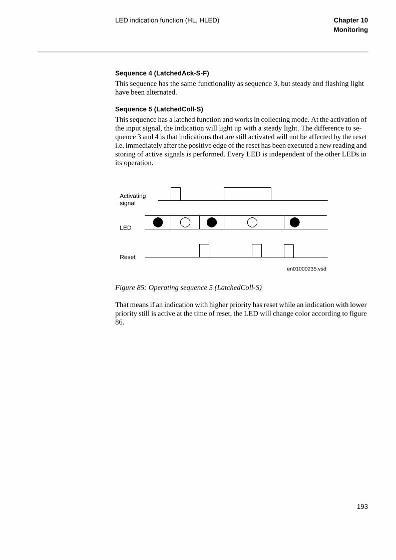
LED indication function (HL, HLED) Chapter 10Monitoring
Sequence 4 (LatchedAck-S-F)
This sequence has the same functionality as sequence 3, but steady and flashing light have been alternated.
Sequence 5 (LatchedColl-S)
This sequence has a latched function and works in collecting mode. At the activation of the input signal, the indication will light up with a steady light. The difference to se-quence 3 and 4 is that indications that are still activated will not be affected by the reset i.e. immediately after the positive edge of the reset has been executed a new reading and storing of active signals is performed. Every LED is independent of the other LEDs in its operation.
Figure 85: Operating sequence 5 (LatchedColl-S)
That means if an indication with higher priority has reset while an indication with lower priority still is active at the time of reset, the LED will change color according to figure 86.
en01000235.vsd
Activatingsignal
LED
Reset
193
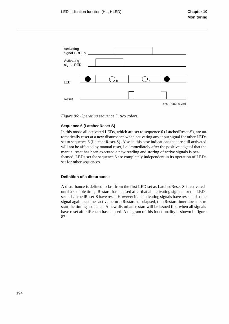
LED indication function (HL, HLED) Chapter 10Monitoring
Figure 86: Operating sequence 5, two colors
Sequence 6 (LatchedReset-S)
In this mode all activated LEDs, which are set to sequence 6 (LatchedReset-S), are au-tomatically reset at a new disturbance when activating any input signal for other LEDs set to sequence 6 (LatchedReset-S). Also in this case indications that are still activated will not be affected by manual reset, i.e. immediately after the positive edge of that the manual reset has been executed a new reading and storing of active signals is per-formed. LEDs set for sequence 6 are completely independent in its operation of LEDs set for other sequences.
Definition of a disturbance
A disturbance is defined to last from the first LED set as LatchedReset-S is activated until a settable time, tRestart, has elapsed after that all activating signals for the LEDs set as LatchedReset-S have reset. However if all activating signals have reset and some signal again becomes active before tRestart has elapsed, the tRestart timer does not re-start the timing sequence. A new disturbance start will be issued first when all signals have reset after tRestart has elapsed. A diagram of this functionality is shown in figure 87.
Activatingsignal RED
LED
Reseten01000236.vsd
Activatingsignal GREEN
R G
194
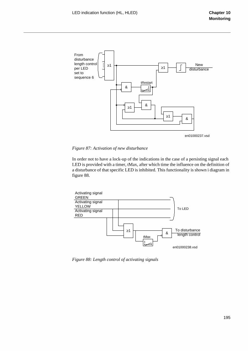
LED indication function (HL, HLED) Chapter 10Monitoring
Figure 87: Activation of new disturbance
In order not to have a lock-up of the indications in the case of a persisting signal each LED is provided with a timer, tMax, after which time the influence on the definition of a disturbance of that specific LED is inhibited. This functionality is shown i diagram in figure 88.
Figure 88: Length control of activating signals
≥1
&
≥1New
disturbance
ttRestart
≥1 &
&≥1
Fromdisturbancelength controlper LEDset tosequence 6
en01000237.vsd
Activating signalGREENActivating signalYELLOWActivating signalRED
≥1
t
tMax&
To disturbancelength control
To LED
en01000238.vsd
195
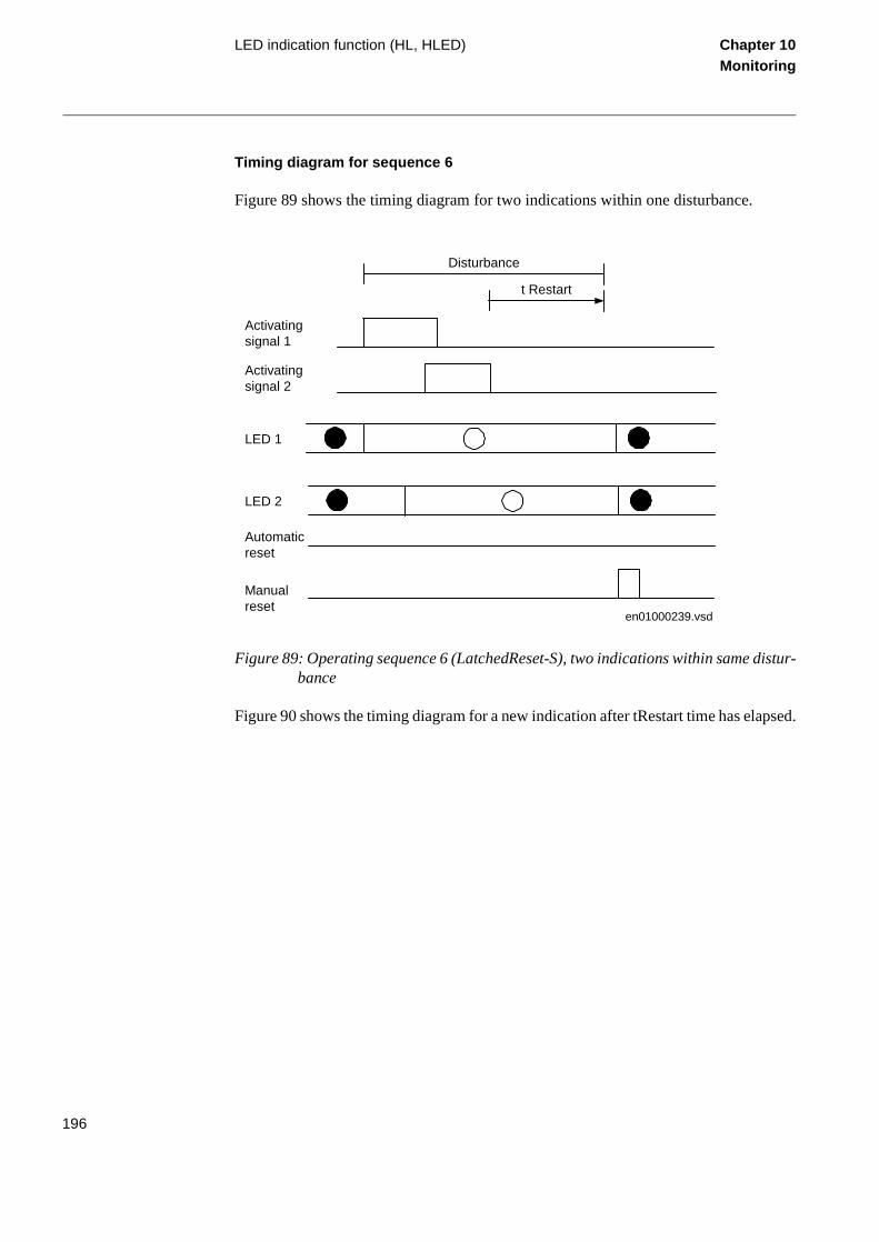
LED indication function (HL, HLED) Chapter 10Monitoring
Timing diagram for sequence 6
Figure 89 shows the timing diagram for two indications within one disturbance.
Figure 89: Operating sequence 6 (LatchedReset-S), two indications within same distur-bance
Figure 90 shows the timing diagram for a new indication after tRestart time has elapsed.
en01000239.vsd
Activatingsignal 2
LED 2
Manualreset
Activatingsignal 1
Automaticreset
LED 1
Disturbance
t Restart
196
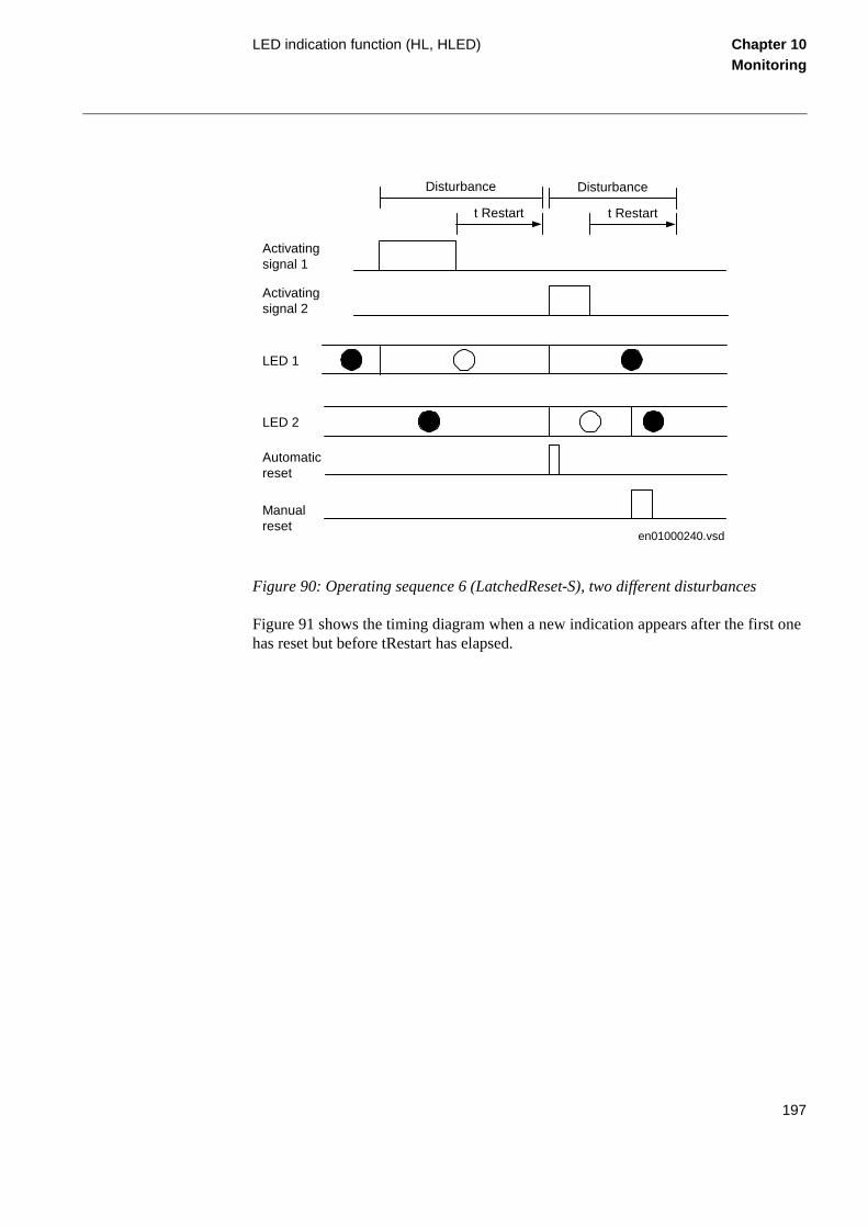
LED indication function (HL, HLED) Chapter 10Monitoring
Figure 90: Operating sequence 6 (LatchedReset-S), two different disturbances
Figure 91 shows the timing diagram when a new indication appears after the first one has reset but before tRestart has elapsed.
en01000240.vsd
Activatingsignal 2
LED 2
Manualreset
Activatingsignal 1
Automaticreset
LED 1
Disturbance
t Restart
Disturbance
t Restart
197
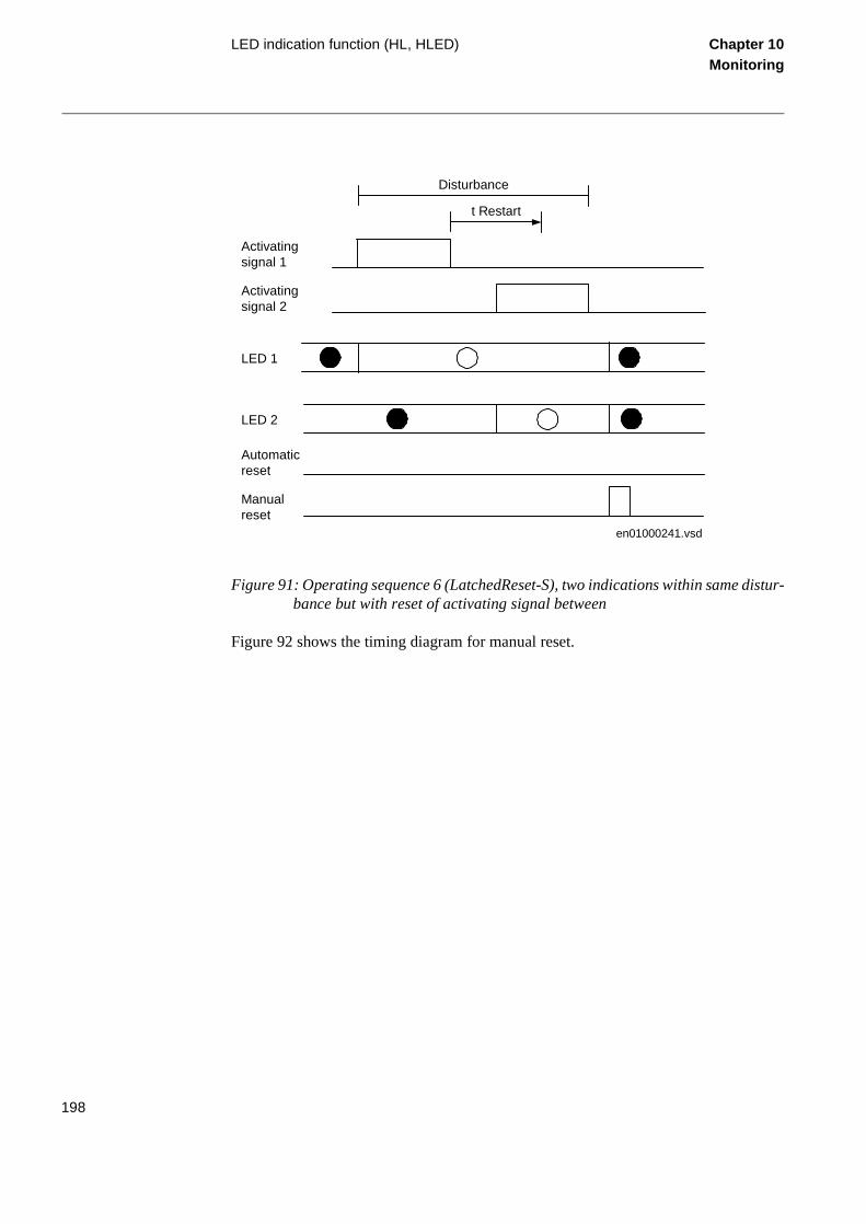
LED indication function (HL, HLED) Chapter 10Monitoring
Figure 91: Operating sequence 6 (LatchedReset-S), two indications within same distur-bance but with reset of activating signal between
Figure 92 shows the timing diagram for manual reset.
en01000241.vsd
Activatingsignal 2
LED 2
Manualreset
Activatingsignal 1
Automaticreset
LED 1
Disturbance
t Restart
198

LED indication function (HL, HLED) Chapter 10Monitoring
Figure 92: Operating sequence 6 (LatchedReset-S), manual reset
1.3 Calculations
Settings can be performed from the local HMI in a separate menu-tree or from the PST. Change of settings is restricted by the activation of a local HMI function.
From the local HMI, the parameters can be set via the sub-menu:
Setting
Functions
Groupx
HMI LED
en01000242.vsd
Activatingsignal 2
LED 2
Manualreset
Activatingsignal 1
Automaticreset
LED 1
Disturbance
t Restart
199
Disturbance report (DRP) Chapter 10Monitoring
ach ns in-
o-
2 Disturbance report (DRP)
2.1 Application
Use the disturbance report to provide the network operator with proper information about disturbances in the primary network. Continuous collection of system data and, at occurrence of a fault, storing of a certain amount of pre-fault, fault and post-fault da-ta, contributes to the highest possible quality of electrical supply. The stored data can be used for analysis and decision making to find and eliminate possible system and equipment weaknesses.
The function comprises several sub functions enabling different users to access relevant information in a structured way.
2.2 Functionality
The disturbance report is a common name for several facilities to supply the operator with more information about the disturbances in the system. Some of the facilities are basic and some are optional in the different products. For some products not all facilities are available.
The facilities included in the disturbance report are:
• General disturbance information
• Indications
• Event recorder
• Fault locator
• Trip values (phase values)
• Disturbance recorder
The whole disturbance report can contain information for up to 10 disturbances, ewith the data coming from all the parts mentioned above, depending on the optiostalled. All information in the disturbance report is stored in non-volatile flash memries. This implies that no information is lost in case of loss-of-power supply
200
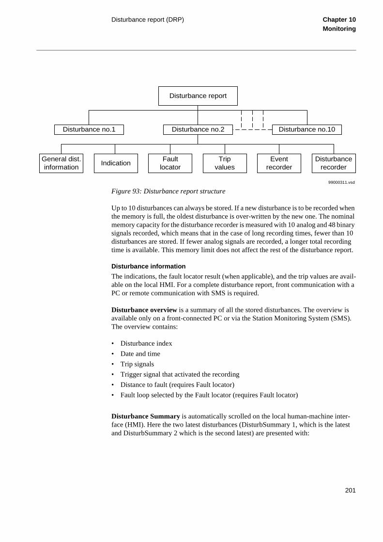
Disturbance report (DRP) Chapter 10Monitoring
-est
Figure 93: Disturbance report structure
Up to 10 disturbances can always be stored. If a new disturbance is to be recorded when the memory is full, the oldest disturbance is over-written by the new one. The nominal memory capacity for the disturbance recorder is measured with 10 analog and 48 binary signals recorded, which means that in the case of long recording times, fewer than 10 disturbances are stored. If fewer analog signals are recorded, a longer total recording time is available. This memory limit does not affect the rest of the disturbance report.
Disturbance information
The indications, the fault locator result (when applicable), and the trip values are avail-able on the local HMI. For a complete disturbance report, front communication with a PC or remote communication with SMS is required.
Disturbance overview is a summary of all the stored disturbances. The overview is available only on a front-connected PC or via the Station Monitoring System (SMS). The overview contains:
• Disturbance index
• Date and time
• Trip signals
• Trigger signal that activated the recording
• Distance to fault (requires Fault locator)
• Fault loop selected by the Fault locator (requires Fault locator)
Disturbance Summary is automatically scrolled on the local human-machine interface (HMI). Here the two latest disturbances (DisturbSummary 1, which is the latand DisturbSummary 2 which is the second latest) are presented with:
Disturbance report
Disturbance no.1 Disturbance no.2 Disturbance no.10
General dist.information
IndicationFault
locatorTrip
valuesEvent
recorderDisturbance
recorder
99000311.vsd
201
Disturbance report (DRP) Chapter 10Monitoring
cator are
r-after
Mon-
mea-eters
ection
the
d after
time-ance
• Date and time
• Selected indications (set with the Indication mask)
• Distance to fault and fault loop selected by the Fault locator
Disturbance data on the HMI is presented at:
DisturbReport/Disturbances/Disturbance n (n=1 - 10)
The date and time of the disturbance, the trigger signal, the indications, the fault loresult and the trip values are available, provided that the corresponding functionsinstalled.
Indications
Indications is a list of signals that were activated during the fault time of the distubance. A part (or all) of these signals are automatically scrolled on the local HMI a disturbance.
Event recorder
The event recorder contains an event list with time-tagged events. In the Station itoring System, this list is directly connected to a disturbance.
Fault locator
The fault locator contains information about the distance to the fault and about thesuring loop that was selected for the calculation. After changing the system paramin the terminal, a recalculation of the distance to the fault can be made in the prot
Trip values
Trip values includes phasors of currents and voltages before the fault and duringfault
Disturbance recorder
The disturbance recorder records analog and binary signal data before, during anthe fault.
Recording times
The disturbance report records information about a disturbance during a settableframe. The recording times are valid for the whole disturbance report. The disturbrecorder and the event recorder register disturbance data and events during tRecording, the total recording time. Indications are only registered during the fault time.
The total recording time, tRecording, of a recorded disturbance is:
202
Disturbance report (DRP) Chapter 10Monitoring
Table 9: Definitions
Figure 94: The recording times definition
Analog signals
Up to 10 analog signals (five voltages and five currents from the transformer module) can be selected for recording and triggering if the disturbance recorder function is in-stalled. If fewer than 10 signals are selected, the maximum storing capacity in the flash memories, regarding total recording time are increased.
A user-defined name for each of the signals can be programmed in the terminal.
tRecording = tPre + tFault + tPost or tPre + tLim, depending on which criterion stops the current disturbance recording
1 Pre-fault or pre-trigger recording time. The time before the fault including the operate time of the trigger. Use the setting tPre to set this time.
2 Fault time of the recording. The fault time cannot be set. It continues as
long as any valid trigger condition, binary or analog, persists (unless limited by tLim the limit time).
3 Post fault recording time. The time the disturbance recording continues
after all activated triggers are reset. Use the setting tPost to set this time.
tLim Limit time. The maximum allowed recording time after the disturbance recording was triggered. The limit time is used to eliminate the conse-
quences of a trigger that does not reset within a reasonable time interval. It limits the maximum recording time of a recording and prevents subsequent overwriting of already stored disturbances.Use the setting tLim to set this
time.
tPre
tLim
tPost
xx00000316.vsd
1 2 3
203

Disturbance report (DRP) Chapter 10Monitoring
For each of the 10 analog signals, Operation = On means that it is recorded by the dis-turbance recorder. The trigger is independent of the setting of Operation, and triggers even if operation is set to Off. Both undervoltage and overvoltage can be used as trigger condition. The same applies for the current signals.
The check of the trigger condition is based on peak-to-peak values. When this is found, the absolute average value of these two peak values is calculated. If the average value is above the threshold level for an overvoltage or overcurrent trigger, this trigger is in-dicated with a greater than (>) sign with the user-defined name.
If the average value is below the set threshold level for an undervoltage or undercurrent trigger, this trigger is indicated with a less than (<) sign with its name. The procedure is separately performed for each channel.
This method of checking the analog start conditions gives a function which is insensi-tive to DC offset in the signal. The operate time for this start is typically in the range of one cycle, 20 ms for a 50 Hz network.
The analog signals are presented only in the disturbance recording, but they affect the entire disturbance report when being used as triggers.
Binary signals
Up to 48 binary signals can be selected from the signal list, where all available signals are grouped under each function. The 48 signals can be selected from internal logical signals and binary input signals. Each of the 48 signals can be selected as a trigger of the disturbance report. It is also possible to set if the trigger should be activated on a logic 1 or a logic 0. A binary signal can be selected to activate the red LED on the local HMI.
A user-defined name for each of the signals can be programmed in the terminal.
The selected 48 signals are presented in the event list and the disturbance recording. But they affect the whole disturbance report when they are used as triggers.
The indications, that are to be automatically scrolled on the HMI when a disturbance has been recorded are also selected from these 48 signals with the HMI Indication Mask.
Trigger signals
The trigger conditions affect the entire disturbance report. As soon as a trigger condition is fulfilled, a complete disturbance report is recorded. On the other hand, if no trigger condition is fulfilled, there is no disturbance report, no calculation of distance to fault, no indications, and so on. This implies the importance of choosing the right signals as trigger conditions.
204
Disturbance report (DRP) Chapter 10Monitoring
cted . This
igger.
ed sig-
d in talled
re-ture
an-
A trigger can be of type:
• Manual trigger
• Binary-signal trigger
• Analog-signal trigger (over/under function)
Manual trigger
A disturbance report can be manually triggered from the local HMI, a front-connePC, or SMS. When the trigger is activated, the manual trigger signal is generatedfeature is especially useful for testing.
Manual trigger from the local HMI is found at:
DisturbReport
ManualTrig
Binary trigger
Any binary signal state (logic one or a logic zero) can be selected to generate a trThe binary signal must remain in a steady state for at least 15 ms to be valid.
When a binary signal is selected to generate a trigger from a logic zero, the selectnal will not be listed in the indications list of the disturbance report.
Analog trigger
All analog signals are available for trigger purposes, no matter if they are recordethe disturbance recorder or not. But the disturbance recorder function must be insin the terminal.
Retrigger
Under certain circumstances the fault condition may reoccur during the postfault cording, for instance by automatic reclosing to a still faulty network. In order to capthe new fault it is possible to allow retriggering during the PostFault recording.
2.3 Calculations
The main part of the settings for the Disturbance Report is found on the local hummachine interface (HMI) at:
205
Disturbance report (DRP) Chapter 10Monitoring
Settings
DisturbReport
The settings include:
User-defined names of analog signals can be set at:
Configuration
AnalogInputs
The user-defined names of binary signals can be set at:
Configuration
DisturbReport
Input n (n=1-48)
The analog and binary signals appear with their user-defined names.
Operation Disturbance Report (On/Off)
ReTrig Re-trigger during post-fault state (On/Off)
SequenceNo Sequence number (0-255) (normally not necessary to set)
RecordingTimes Recording times for the Disturbance Report and the event/indication logging, including pre-fault time, post-fault time, and limit time for the
entire disturbance
BinarySignals Selection of binary signals, trigger conditions, HMI indication mask and HMI red LED option
AnalogSignals Recording mask and trigger conditions
FaultLocator Distance measurement unit (km/miles/%)
km or miles selected under line reference
206
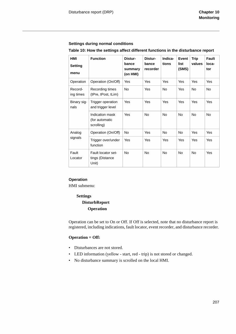
Disturbance report (DRP) Chapter 10Monitoring
Settings during normal conditions
Table 10: How the settings affect different functions in the disturbance report
Operation
HMI submenu:
Settings
DisturbReport
Operation
Operation can be set to On or Off. If Off is selected, note that no disturbance report is registered, including indications, fault locator, event recorder, and disturbance recorder.
Operation = Off:
• Disturbances are not stored.
• LED information (yellow - start, red - trip) is not stored or changed.
• No disturbance summary is scrolled on the local HMI.
HMI
Setting
menu
Function Distur-bance summary (on HMI)
Distur-bance recorder
Indica-tions
Event list (SMS)
Trip values
Fault loca-tor
Operation Operation (On/Off) Yes Yes Yes Yes Yes Yes
Record-ing times
Recording times (tPre, tPost, tLim)
No Yes No Yes No No
Binary sig-
nals
Trigger operation
and trigger level
Yes Yes Yes Yes Yes Yes
Indication mask (for automatic
scrolling)
Yes No No No No No
Analog signals
Operation (On/Off) No Yes No No Yes Yes
Trigger over/under
function
Yes Yes Yes Yes Yes Yes
Fault Locator
Fault locator set-tings (Distance
Unit)
No No No No No Yes
207

Disturbance report (DRP) Chapter 10Monitoring
from
lat-
ber in
will
e until
Operation = On:
• Disturbances are stored, disturbance data can be read from the local HMI anda front-connected PC or Station Monitoring System (SMS).
• LED information (yellow - start, red - trip) is stored.
• The disturbance summary is automatically scrolled on the local HMI for the twoest registered disturbances, until cleared.
Post re-trigger can be set to On or Off
Postretrig = On:
Re-trigger during the set post-fault time is enabled.
Postretrig = Off:
Re-trigger during the set post fault time is not accepted.
Sequence number
HMI submenu:
Settings
DisturbReport
SequenceNo
Normally, this setting option is seldom used. Each disturbance is assigned a numthe disturbance report. The first disturbance each day normally receives SequenceNo = 0. The value of SequenceNo that can be read in the service report is the number that be assigned to the next disturbance registered during that day.
In normal use, the sequence number is increased by one for each new disturbancit is reset to zero each midnight.
Recording times
HMI submenu:
208
Disturbance report (DRP) Chapter 10Monitoring
Settings
DisturbReport
RecordingTimes
Under this submenu, the different recording times for the disturbance report are set (the pre-fault time, post-fault time, and limit time). These recording times affect the distur-bance recorder and event recorder functions. The total recording time, tRecording, of a recorded disturbance is:
Binary signals
HMI submenu:
Configuration
DisturbReport
Input n (n=1-48)
Up to 48 binary signals can be selected from the signal list, where all available signals are grouped function by function. The 48 signals can be selected among internal logical signals and binary input signals. Each selected signal is registered by the disturbance recorder, event recorder, and indication functions during a recording.
A user-defined name for each of the signals can be entered. This name can comprise up to 13 characters.
HMI submenu:
Settings
DisturbReport
BinarySignals
For each of the 48 signals, it is also possible to select if the signal is to be used as a trig-ger for the start of the disturbance report (TrigOperation), and if the trigger should be activated at a logical 1 or 0 level (TrigLevel).
tRecording = tPre + tFault + tPost, or tPre + tLim, depending on which criterion stops the
current disturbance recording.
209

Disturbance report (DRP) Chapter 10Monitoring
The indications in the disturbance summary, that are automatically scrolled on the HMI when a disturbance is registered, are also selected from these 48 signals using the indi-cation mask.
Analog signals
HMI submenu:
Settings
DisturbReport
AnalogSignals
This HMI submenu is only available when the disturbance recorder option is installed. For each of the 10 analog signals (five voltages and five currents), Operation = On means that it is recorded by the disturbance recorder. If fewer than 10 signals are select-ed, the maximum storing capacity in the flash memories for total recording time be-comes longer.
Both undervoltage and overvoltage can be used as trigger condition. The same applies for the current signals. The trigger is independent of the setting of Operation and trig-gers even if Operation = Off.
A user-defined name for each of the signals can be entered. It can consist of up to 13 characters. It is found at:
Configuration
AnalogInputs
Behaviour during test mode
When the terminal is set to test mode, the behaviour of the disturbance report can be controlled by the test mode disturbance report settings Operation and DisturbSumma-ry available on the local HMI under:
Test/Testmode/DisturbReport
The impact of the settings are according to the following table:
210

Disturbance report (DRP) Chapter 10Monitoring
Table 11: Disturbance report settings
Operation Disturb-Summary
Then the results are...
Off Off • Disturbances are not stored.
• LED information is not displayed on the HMI and not stored.
• No disturbance summary is scrolled on the HMI.
Off On • Disturbances are not stored.
• LED information (yellow - start, red - trip) are displayed on the local HMI but not stored in the terminal.
• Disturbance summary is scrolled automatically on the local HMI for the two latest recorded disturbances, until cleared.
• The information is not stored in the terminal.
On On or Off • The disturbance report works as in normal mode.
• Disturbances are stored. Data can be read from the local HMI, a front-connected PC, or SMS.- LED information (yellow - start, red - trip) is stored.
• The disturbance summary is scrolled automatically on the local HMI for the two latest recorded disturbances, until cleared.
• All disturbance data that is stored during test mode remains in the terminal when changing back to normal mode.
211
Indications Chapter 10Monitoring
hni-
3 Indications
3.1 Application
The indications from all the 48 selected binary signals are shown on the local human-machine interface (HMI) and on the Station Monitoring System (SMS) for each record-ed disturbance in the disturbance report. The LEDs on the front of the terminal display start and trip indications.
3.2 Functionality
The indications shown on the HMI and SMS give an overview of the status of the 48 event signals during the fault. On the HMI, the indications for each recorded distur-bance are presented at:
DisturbReport
Disturbances
Disturbance n (n=1-10)
All selected signals can be internally produced signals or emerge from binary input channels.
The indications are registered only during the fault time of a recorded disturbance, as long as any trigger condition is activated. A part or all of these indications can be auto-matically scrolled on the local HMI after a disturbance is recorded, until acknowledged with the C button on the HMI. They are selected with the indication mask.
The signal name for internal logical signals presented on the screen follows the signal name, which can be found in the signal list in each function description of the “Teccal reference manual”. Binary input signals are displayed with their user-defined names.
The LED indications display this information:
Green LED:
• Steady light In Service
• Flashing light Internal fail, the INT--FAIL internal signal is high
• Dark No power supply
212

Indications Chapter 10Monitoring
3.3 Calculations
The signals to be displayed as indications are selected in the disturbance report setting. This can be found on the local HMI at:
Settings
DisturbReport
BinarySignals
Input n (n=1-48)
Yellow LED:
• Steady light A disturbance report is triggered
• Flashing light The terminal is in test mode or in configuration mode
Red LED:
• Steady light Trig on binary signal with HMI red LED option set
• Flashing light The terminal is in configuration mode
213
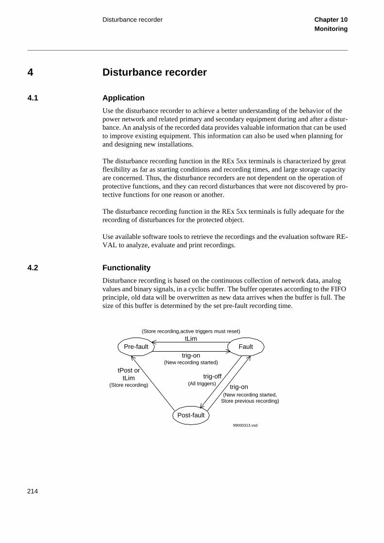
Disturbance recorder Chapter 10Monitoring
4 Disturbance recorder
4.1 Application
Use the disturbance recorder to achieve a better understanding of the behavior of the power network and related primary and secondary equipment during and after a distur-bance. An analysis of the recorded data provides valuable information that can be used to improve existing equipment. This information can also be used when planning for and designing new installations.
The disturbance recording function in the REx 5xx terminals is characterized by great flexibility as far as starting conditions and recording times, and large storage capacity are concerned. Thus, the disturbance recorders are not dependent on the operation of protective functions, and they can record disturbances that were not discovered by pro-tective functions for one reason or another.
The disturbance recording function in the REx 5xx terminals is fully adequate for the recording of disturbances for the protected object.
Use available software tools to retrieve the recordings and the evaluation software RE-VAL to analyze, evaluate and print recordings.
4.2 Functionality
Disturbance recording is based on the continuous collection of network data, analog values and binary signals, in a cyclic buffer. The buffer operates according to the FIFO principle, old data will be overwritten as new data arrives when the buffer is full. The size of this buffer is determined by the set pre-fault recording time.
Pre-fault Fault
Post-fault
(Store recording,active triggers must reset)
tLim
trig-on(New recording started)
trig-off(All triggers)
tPost ortLim
(Store recording) trig-on(New recording started,
Store previous recording)
99000313.vsd
214
Disturbance recorder Chapter 10Monitoring
Upon detection of a fault condition (triggering), the data storage continues in another part of the memory. The storing goes on as long as the fault condition prevails - plus a certain additional time. The length of this additional part is called the post-fault time and it can be set in the disturbance report. The above mentioned two parts form a dis-turbance recording. The whole memory acts as a cyclic buffer and when it is full, the oldest recording is overwritten.
A user-defined name for each of the signals can be programmed in the terminal.
Recording Capacity
The recording function can record all analog inputs in the transformer module and up to 48 binary signals. To maximise the use of the memory, the number of analog chan-nels to be recorded is user-selectable by programming and can be set individually for each analog input. The recorded binary signals can be either true binary input signals or internal logical signals created by the functions.
Memory capacity
The maximum number of recordings stored in the memory is 10. So depending on the set recording times and the recording of the enabled number of channels, the memory can contain a minimum of six and a maximum of 10 disturbance recordings comprising of both header part and data part. But the header part for the last 10 recordings is always available.
Time tagging
The terminal has a built-in, real-time clock and calendar. This function is used for time tagging of the recorded disturbances. The time tagging refers to the activation of the trigger that starts the disturbance recording.
Signal processing
The processing of analog signals is handled by a dedicated DSP (digital signal proces-sor). Other functions are implemented in the main CPU. The memory is shared with other functions.
The numerical signals coming from the A/D conversion module in serial form are con-verted to parallel form in a dedicated DSP. The analog trigger conditions are also checked in the DSP.
A check of the start conditions is performed by searching for a maximum value. This is a positive peak. The function also seeks a minimum value, which is the negative peak.
When this is found, the absolute average value is calculated. If this value is above the set threshold level for the overfunction on the channel in question, an overfunction start on that channel is indicated. The overfunction is indicated with a greater than (>) sign.
215
Disturbance recorder Chapter 10Monitoring
r in-
in a e
Thus, t, and
ne for (tPre) t
orded trig-
ls
com-the da-
Similarly, if the average value is below the set threshold level for underfunction on the channel in question, an underfunction start on that channel is indicated. The underfunc-tion is indicated with a less than (<) sign.
The procedure is separately performed for each channel. This method of checking the analog start conditions gives a function that is insensitive to DC offset in the signal. The operating time for this start is typically in the range of one cycle, 20 ms in a 50 Hz net-work.
The numerical data, along with the result of the trigger condition evaluation, are trans-mitted to the main CPU. The main CPU handles these functions:
• Evaluation of the manual start condition
• Evaluation of the binary start condition, both for true binary input signals and foternally created logical signals
• Storage of the numerical values for the analog channels
The numerical data for the analog channels are stored in a cyclic pre-fault buffer RAM. When a trigger is activated, the data storage is moved to another area in thRAM, where the data for the fault and the subsequent post-fault period are stored.a complete disturbance recording comprises the stored data for the pre-fault, faulpost-fault period.
The RAM area for temporary storage of recorded data is divided into sub-areas, oeach recording. The size of a subarea is governed by the sum of the set pre-faultand maximum post-trigger (tLim) time. There is a sufficient memory capacity for aleast four consecutive recordings with a maximum number of analog channels recand with maximum time settings. Should no such area be free at the time of a newger, the oldest recording stored in the RAM is overwritten.
When a recording is completed, a post recording processing occurs.
This post-recording processing comprises:
• Merging the data for analog channels with corresponding data for binary signastored in an event buffer
• Compression of the data, which is performed without losing any data accuracy
• Storing the compressed data in a non-volatile memory (flash memory)
The recorded disturbance is now ready for retrieval and evaluation. The recordingprises the stored and time-tagged disturbance data along with relevant data from tabase for configuration and parameter set-up.
216

Disturbance recorder Chapter 10Monitoring
Some parameters in the header of a recording are stored with the recording, and some are retrieved from the parameter database in connection with a disturbance. This means that if a parameter that is retrieved from the parameter database was changed between the time of recording and retrieval, the collected information is not correct in all parts. For this reason, all recordings should be transferred to the Station Monitoring System (SMS) workstation and then deleted in the terminal before any such parameters are changed.
4.3 Design
The recordings can be divided into two parts, the header and the data part. The data part contains the numerical values of recorded analog and binary channels. The header con-tains clearly written basic information about the disturbance. A part of this information is also used by REVAL to reproduce the analog and binary signals in a correct and user-friendly way. Such information is primary and secondary instrument transformer rat-ings.
Table 12: Disturbance header
Parameter Parameter data-base
Stored with distur-ance
General
Station, object and ID x
Date and time x
Sequence number x
CT earthing x
Time synchronization source x
Collection window parameters tPre, tPost, tLim
x
Prefault phase-to-phase voltage
and current RMS values
x
Trig signal and test flag x
Analog signals
Signal name x
Primary and secondary instrument transformer rating
x
Undertrig: level and operation x
Overtrig: level and operation x
217
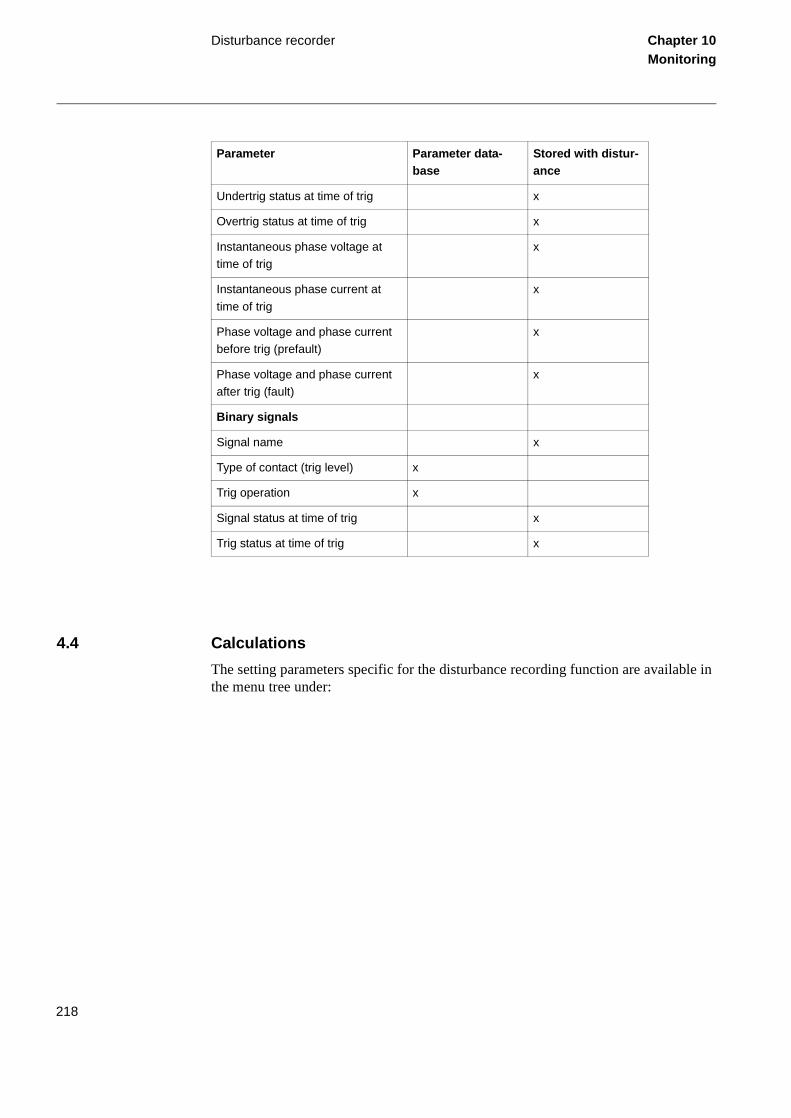
Disturbance recorder Chapter 10Monitoring
4.4 Calculations
The setting parameters specific for the disturbance recording function are available in the menu tree under:
Undertrig status at time of trig x
Overtrig status at time of trig x
Instantaneous phase voltage at time of trig
x
Instantaneous phase current at
time of trig
x
Phase voltage and phase current before trig (prefault)
x
Phase voltage and phase current after trig (fault)
x
Binary signals
Signal name x
Type of contact (trig level) x
Trig operation x
Signal status at time of trig x
Trig status at time of trig x
Parameter Parameter data-base
Stored with distur-ance
218
Disturbance recorder Chapter 10Monitoring
f the
o the iden-
ce re- the e-
nce in- se-
Settings
DisturbReport
Operation
SequenceNo
RecordingTimes
BinarySignals
AnalogSignals
The list of parameters in the “Technical reference manual”, explains the meaning oabbreviations used in connection with setting ranges.
Remember that values of parameters set elsewhere in the menu tree are linked tinformation on a recording. Such parameters are, for example, station and objecttifiers, CT and PT ratios.
The sequence number of the recordings is a specific parameter for the disturbancorder and is used to identify the different recordings. By combining the date andsequence number for a recording, the recording can be uniquely identified. The squence number is also shown under:
Settings
DisturbReport
SequenceNo
The read value on the local human-machine interface (HMI) display is the sequenumber that the next recorded disturbance receives. The number is automaticallycreased by one for each new recording and is reset to zero at each midnight. Thequence number can also be set manually.
219
Event recorder Chapter 10Monitoring
5 Event recorder
5.1 Application
When using a front-connected PC or Station Monitoring System (SMS), an event list can be available for each of the recorded disturbances in the disturbance report. Each list can contain up to 150 time-tagged events. These events are logged during the total recording time, which depends on the set recording times (pre-fault, post-fault and limit time) and the actual fault time. During this time, the first 150 events for all the 48 se-lected binary signals are logged and time tagged. This list is a useful instrument for evaluating a fault and is a complement to the disturbance recorder.
To obtain this event list, the event recorder function (basic in some terminals and op-tional in others) must be installed.
5.2 Functionality
When one of the trig conditions for the disturbance report is activated, the events are collected by the main processing unit, from the 48 selected binary signals. The events can come from both internal logical signals and binary input channels. The internal sig-nals are time tagged in the main processing module, while the binary input channels are time tagged directly on each I/O module. The events are collected during the total re-cording time, tRecording, and they are stored in the disturbance report memory at the end of each recording.
The name of the binary input signal that appears in the event list is the user-defined name that can be programmed in the terminal.
The time tagging of events emerging from internal logical signals and binary input channels has a resolution of 1 ms.
5.3 Calculations
The settings of the event recorder consist of the signal selection and the recording times. It is possible to select up to 48 binary signals, either internal signals or signals coming from binary input channels. These signals coincide with the binary signals recorded by the disturbance recorder. The disturbance summary indications that are to scroll auto-matically on the local human-machine interface (HMI), can only be selected from these 48 event channels.
The signal selection is found at:
220
Event recorder Chapter 10Monitoring
Settings
DisturbReport
BinarySignals
Input n (n=1-48)
Each of the up to 48 event channels can be selected from the signal list, consisting of all available internal logical signals and all binary input channels.
For each of the binary input and output signals, a user-defined name can be pro-grammed at:
Configuration
I/O
Slotnn-XXXX (ex. Slot15-BOM3)
221

Trip value recorder Chapter 10Monitoring
6 Trip value recorder
6.1 Application
The main objective of line protection and monitoring terminals is fast, selective and re-liable operation for faults on a protected object. Besides this, information on the values of the currents and voltages before and during the fault is valuable to understand the se-verity of the fault.
The trip value recorder in the REx 5xx series of terminals provides this information on the HMI and via SCS/SMS. The function is an optional software module in the terminal.
The function calculates the pre-fault and fault values of currents and voltages and pre-sents them as phasors with amplitude and argument.
6.2 Design
Pre-fault and fault phasors of currents and voltages are filtered from disturbance data stored in digital sample buffers.
When the disturbance report function is triggered, the trip value recorder function starts to calculate the frequency of the analogue channel U1. If the calculation fails, a default frequency is read from database to ensure further execution of the function.
Then the sample for the fault interception is looked for by checking the non-periodic changes. The channel search order is U1, U2, U3, I1, I2, I3, I4, I5 and U5.
If no error sample is found, the trig sample is used as the start sample for the Fourier estimation of the complex values of currents and voltages. The estimation uses samples during one period before the trig sample. In this case the calculated values are used both as pre-fault and fault values.
If an error sample is found the Fourier estimation of the prefault values starts 1.5 period before the fault sample. The estimation uses samples during one period. The postfault values are calculated using the Recursive Least Squares (RLS) method. The calculation starts a few samples after the fault sample and uses samples during 1/2 - 2 periods de-pending on the shape of the signals.
The pre-fault time (tPre) should be at least 0.1 s to ensure enough samples for the esti-mation of pre-fault trip values.
222

Trip value recorder Chapter 10Monitoring
6.3 Calculations
Customer specific names for all the ten analogue inputs (five currents and five voltages) can be entered. Each name can have up to 13 alphanumeric characters. These names are common for all functions within the disturbance report functionality.
The user-defined names for the analogue inputs are set under the menu:
Configuration
AnalogInputs
U1 (U2..U5, I1..I5)
223
Monitoring of AC analog measurements Chapter 10Monitoring
ltage ts and nd tective
nd ower
tion- five
on the
els.
nels.
e mea-
age
tage
7 Monitoring of AC analog measurements
7.1 Application
Fast, reliable supervision of different analogue quantities is of vital importance during the normal operation of a power system.
Operators in the control centres can, for example:
• Continuously follow active and reactive power flow in the network
• Supervise the busbar voltage and frequency
Different measuring methods are available for different quantities. Current and voinstrument transformers provide the basic information on measured phase currenvoltages in different points within the power system. At the same time, currents avoltages serve as the input measuring quantities to power and energy meters, prodevices and so on.
Further processing of this information occurs within different control, protection, amonitoring terminals and within the higher hierarchical systems in the secondary psystem.
7.2 Functionality
The REx 5xx protection, control, and monitoring terminals have as basic the funcality to measure and further process information about up to five input currents andinput voltages. The number of processed alternate measuring quantities dependstype of terminal and built-in options. Additional information is also available:
• Mean values of measured currents I in the first three current measuring chann
• Mean values of measured voltages U in the first three voltage measuring chan
• Three-phase active power P as measured by the first three current and voltagsuring channels.
• Three-phase reactive power Q as measured by the first three current and voltmeasuring channels.
• Three-phase apparent power S as measured by the first three current and volmeasuring channels.
• Frequency f.
224
Monitoring of AC analog measurements Chapter 10Monitoring
his al-uantity the
f four f op-
-set
Low-
The accuracy of measurement depends on the requirements. Basic accuracy satisfies the operating (information) needs. An additional calibration of measuring channels is nec-essary and must be ordered separately when the requirements on accuracy of the mea-surement are higher. Refer to the technical data and ordering particulars for the particular terminal.
The information on measured quantities is then available for the user at different loca-tions:
• Locally by means of the local human-machine interface (HMI) unit.
• Locally by means of a front-connected personal computer (PC).
• Remotely over the LON bus to the station control system (SCS)
• Remotely over the SPA port to the station monitoring system (SMS).
User-defined measuring ranges
Each measuring channel has an independent measuring range from the others. Tlows the users to select the most suitable measuring range for each measuring qon each monitored object of the power system. This gives a possibility to optimizefunctionality of the power system.
Continuous monitoring of the measured quantity
Users can continuously monitor the measured quantity in each channel by means obuilt-in operating thresholds (figure 95). The monitoring has two different modes oerating:
• Overfunction, when the measured current exceeds the HiWarn or HiAlarm prevalues.
• Underfunction, when the measured current decreases under the LowWarn or Alarm pre-set values.
225
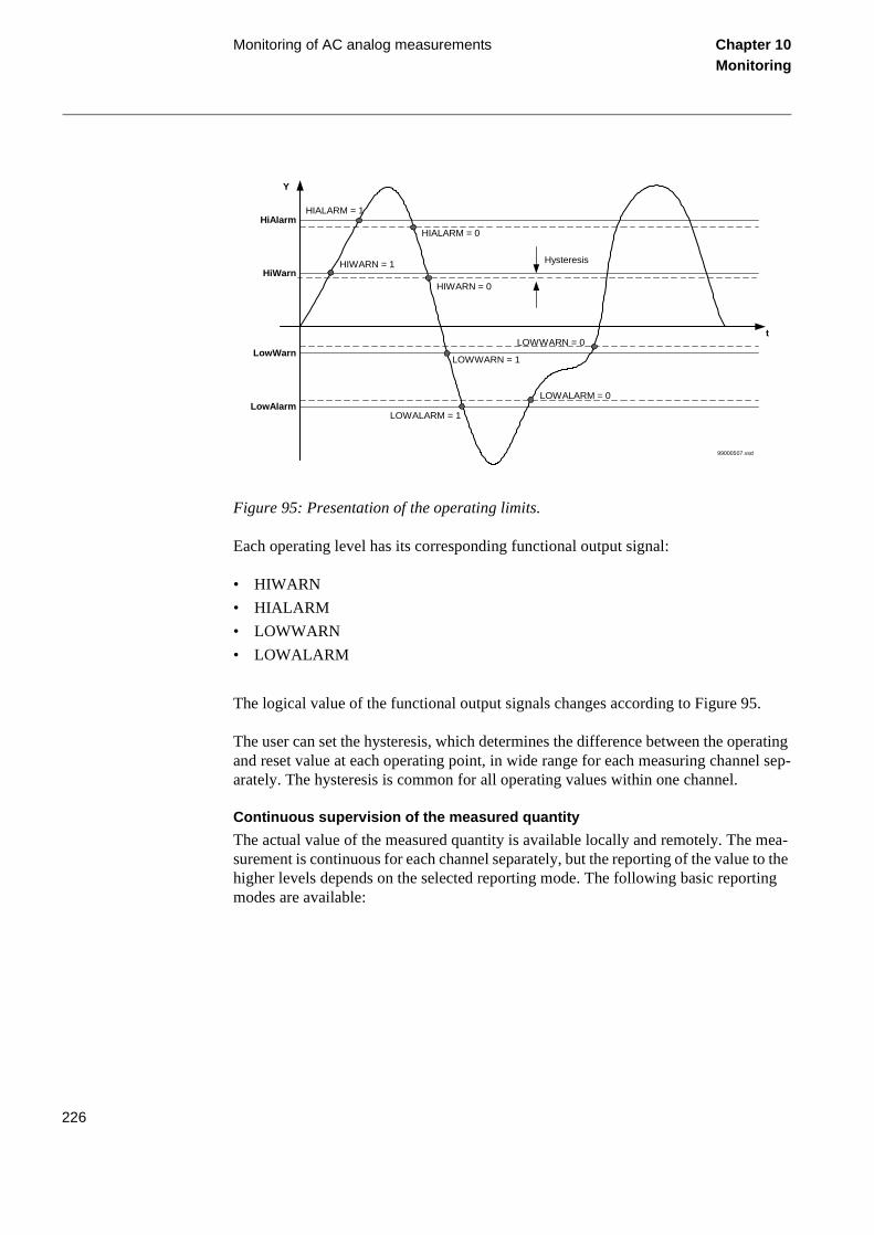
Monitoring of AC analog measurements Chapter 10Monitoring
.
erating el sep-
mea- to the ting
Figure 95: Presentation of the operating limits.
Each operating level has its corresponding functional output signal:
• HIWARN
• HIALARM
• LOWWARN
• LOWALARM
The logical value of the functional output signals changes according to Figure 95
The user can set the hysteresis, which determines the difference between the opand reset value at each operating point, in wide range for each measuring channarately. The hysteresis is common for all operating values within one channel.
Continuous supervision of the measured quantity
The actual value of the measured quantity is available locally and remotely. The surement is continuous for each channel separately, but the reporting of the valuehigher levels depends on the selected reporting mode. The following basic repormodes are available:
99000507.vsd
HIWARN = 1
HIALARM = 1
HIWARN = 0
HIALARM = 0
Hysteresis
HiAlarm
HiWarn
LowWarn
LowAlarm
LOWWARN = 1
LOWALARM = 1
LOWALARM = 0
LOWWARN = 0
Y
t
226
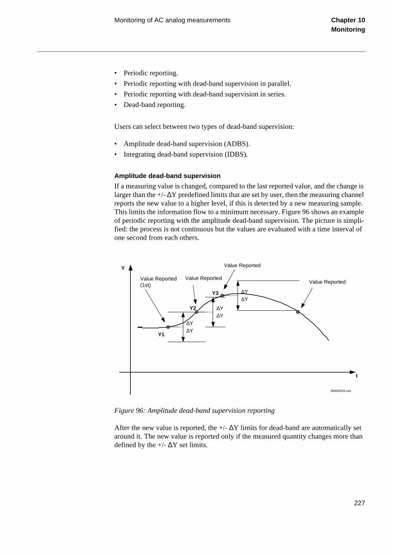
Monitoring of AC analog measurements Chapter 10Monitoring
nge is nnel mple.
ple pli-al of
than
• Periodic reporting.
• Periodic reporting with dead-band supervision in parallel.
• Periodic reporting with dead-band supervision in series.
• Dead-band reporting.
Users can select between two types of dead-band supervision:
• Amplitude dead-band supervision (ADBS).
• Integrating dead-band supervision (IDBS).
Amplitude dead-band supervision
If a measuring value is changed, compared to the last reported value, and the chalarger than the +/- ∆Y predefined limits that are set by user, then the measuring chareports the new value to a higher level, if this is detected by a new measuring saThis limits the information flow to a minimum necessary. Figure 96 shows an examof periodic reporting with the amplitude dead-band supervision. The picture is simfied: the process is not continuous but the values are evaluated with a time intervone second from each others.
Figure 96: Amplitude dead-band supervision reporting
After the new value is reported, the +/- ∆Y limits for dead-band are automatically setaround it. The new value is reported only if the measured quantity changes moredefined by the +/- ∆Y set limits.
99000529.vsd
Y
t
Value Reported(1st)
Value ReportedValue Reported
Y1
Y2
Y3
∆Y∆Y
∆Y∆Y
∆Y∆Y
Value Reported
227
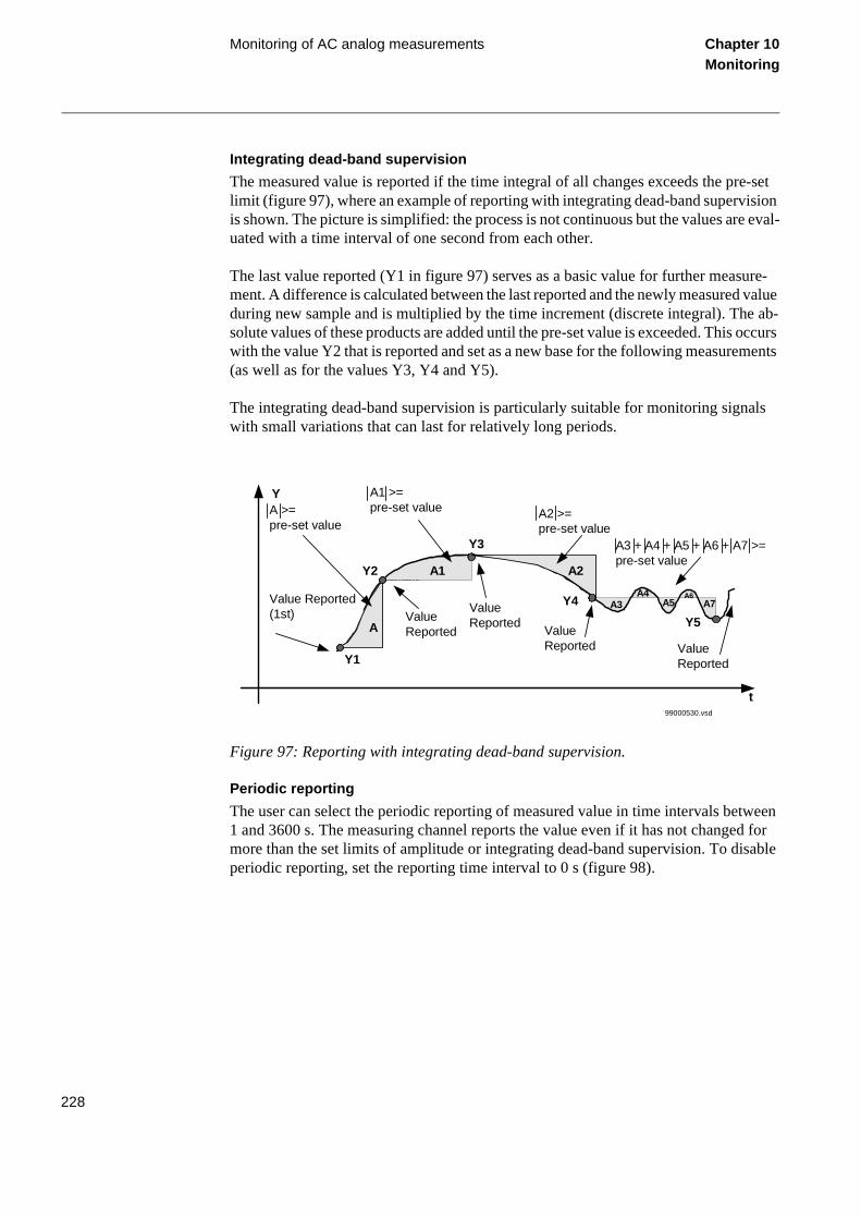
Monitoring of AC analog measurements Chapter 10Monitoring
Integrating dead-band supervision
The measured value is reported if the time integral of all changes exceeds the pre-set limit (figure 97), where an example of reporting with integrating dead-band supervision is shown. The picture is simplified: the process is not continuous but the values are eval-uated with a time interval of one second from each other.
The last value reported (Y1 in figure 97) serves as a basic value for further measure-ment. A difference is calculated between the last reported and the newly measured value during new sample and is multiplied by the time increment (discrete integral). The ab-solute values of these products are added until the pre-set value is exceeded. This occurs with the value Y2 that is reported and set as a new base for the following measurements (as well as for the values Y3, Y4 and Y5).
The integrating dead-band supervision is particularly suitable for monitoring signals with small variations that can last for relatively long periods.
Figure 97: Reporting with integrating dead-band supervision.
Periodic reporting
The user can select the periodic reporting of measured value in time intervals between 1 and 3600 s. The measuring channel reports the value even if it has not changed for more than the set limits of amplitude or integrating dead-band supervision. To disable periodic reporting, set the reporting time interval to 0 s (figure 98).
99000530.vsd
Y
t
Value Reported(1st)
Y1
ValueReported
A1Y2
ValueReported
Y3
Y4
AValueReported
A2
Y5A3
A4A5 A7
A6
ValueReported
A2 >=pre-set value
A1 >=pre-set valueA >=
pre-set value
A3 + A4 + A5 + A6 + A7 >=pre-set value
228
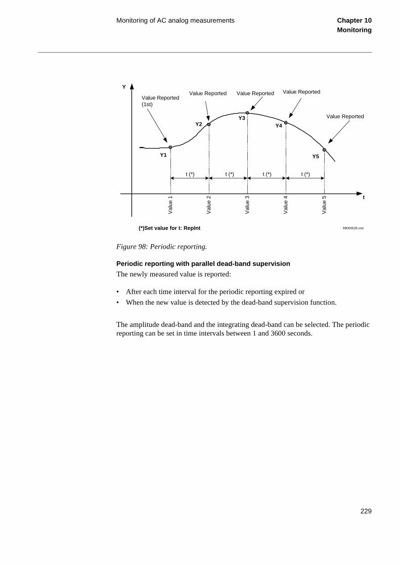
Monitoring of AC analog measurements Chapter 10Monitoring
riodic
Figure 98: Periodic reporting.
Periodic reporting with parallel dead-band supervision
The newly measured value is reported:
• After each time interval for the periodic reporting expired or
• When the new value is detected by the dead-band supervision function.
The amplitude dead-band and the integrating dead-band can be selected. The pereporting can be set in time intervals between 1 and 3600 seconds.
99000528.vsd
Val
ue 1
Y
t
Val
ue 2
Val
ue 3
Val
ue 4
Value Reported(1st)
Value Reported
Val
ue 5
Value Reported
Y1
Y2
Y5
Value Reported Value Reported
Y3Y4
(*)Set value for t: RepInt
t (*) t (*) t (*) t (*)
229
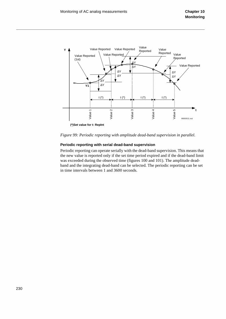
Monitoring of AC analog measurements Chapter 10Monitoring
Figure 99: Periodic reporting with amplitude dead-band supervision in parallel.
Periodic reporting with serial dead-band supervision
Periodic reporting can operate serially with the dead-band supervision. This means that the new value is reported only if the set time period expired and if the dead-band limit was exceeded during the observed time (figures 100 and 101). The amplitude dead-band and the integrating dead-band can be selected. The periodic reporting can be set in time intervals between 1 and 3600 seconds.
99000531.vsdVal
ue 1
Y
tV
alue
2
Val
ue 3
Val
ue 4
Value Reported(1st)
Value ReportedValueReported
Val
ue 5
Value Reported
Y1
∆Y∆Y
ValueReported
t (*) t (*) t (*) t (*)
(*)Set value for t: RepInt
Value Reported
∆Y∆Y
Value Reported
∆Y∆Y
ValueReported
∆Y∆Y
230
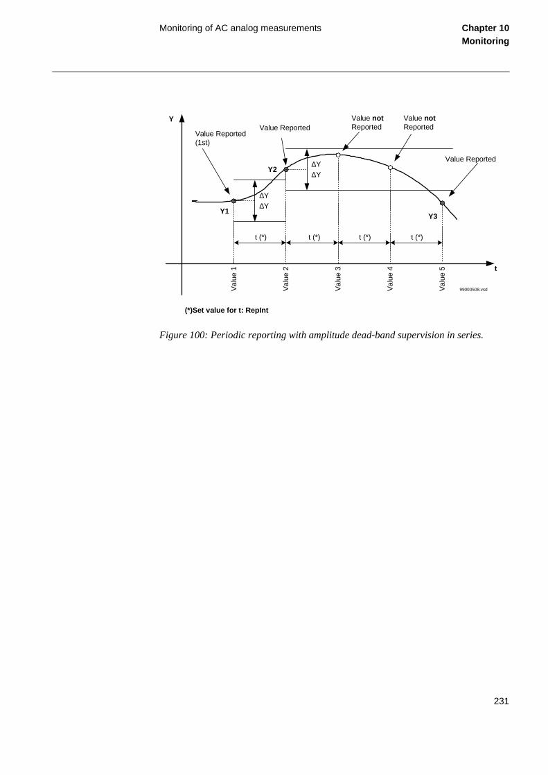
Monitoring of AC analog measurements Chapter 10Monitoring
Figure 100: Periodic reporting with amplitude dead-band supervision in series.
99000508.vsdVal
ue 1
Y
t
Val
ue 2
Val
ue 3
Val
ue 4
Value Reported(1st)
Value Reported
∆Y∆Y
Value notReported
Val
ue 5
Value Reported
Y1
Y2
Y3
∆Y∆Y
Value notReported
t (*) t (*) t (*) t (*)
(*)Set value for t: RepInt
231
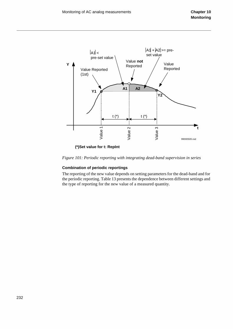
Monitoring of AC analog measurements Chapter 10Monitoring
Figure 101: Periodic reporting with integrating dead-band supervision in series
Combination of periodic reportings
The reporting of the new value depends on setting parameters for the dead-band and for the periodic reporting. Table 13 presents the dependence between different settings and the type of reporting for the new value of a measured quantity.
99000509.vsd
Y
t
Val
ue 1
Val
ue 2
Val
ue 3
Value Reported(1st)
Value notReported
Y1
ValueReported
A1 A2
Y2
t (*) t (*)
(*)Set value for t: RepInt
A1 <pre-set value
A1 + A2 >= pre-set value
232
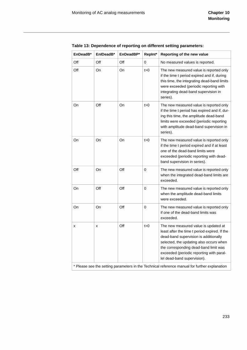
Monitoring of AC analog measurements Chapter 10Monitoring
Table 13: Dependence of reporting on different setting parameters:
EnDeadB* EnIDeadB* EnDeadBP* RepInt* Reporting of the new value
Off Off Off 0 No measured values is reported.
Off On On t>0 The new measured value is reported only if the time t period expired and if, during
this time, the integrating dead-band limits were exceeded (periodic reporting with integrating dead-band supervision in
series).
On Off On t>0 The new measured value is reported only if the time t period has expired and if, dur-
ing this time, the amplitude dead-band limits were exceeded (periodic reporting with amplitude dead-band supervision in
series).
On On On t>0 The new measured value is reported only if the time t period expired and if at least
one of the dead-band limits were exceeded (periodic reporting with dead-band supervision in series).
Off On Off 0 The new measured value is reported only when the integrated dead-band limits are exceeded.
On Off Off 0 The new measured value is reported only when the amplitude dead-band limits were exceeded.
On On Off 0 The new measured value is reported only if one of the dead-band limits was exceeded.
x x Off t>0 The new measured value is updated at least after the time t period expired. If the dead-band supervision is additionally
selected, the updating also occurs when the corresponding dead-band limit was exceeded (periodic reporting with paral-
lel dead-band supervision).
* Please see the setting parameters in the Technical reference manual for further explanation
233
Monitoring of AC analog measurements Chapter 10Monitoring
first
voltag-
d volt-
d volt-
7.3 Design
The design of the alternating quantities measuring function follows the design of all REx 5xx-series protection, control, and monitoring terminals that have distributed func-tionality, where the decision levels are placed as closely as possible to the process.
The measuring function uses the same input current and voltage signals as other protec-tion and monitoring functions within the terminals. The number of input current and voltage transformers depends on the type of terminal and options included. The maxi-mum possible configuration comprises five current and five voltage input channels.
Measured input currents and voltages are first filtered in analogue filters and then con-verted to numerical information by an A/D converter, which operates with a sampling frequency of 2 kHz.
The numerical information on measured currents and voltages continues over a serial link to one of the built-in digital signal processors (DSP). An additional Fourier filter numerically filters the received information, and the DSP calculates the corresponding values for the following quantities:
• Five input measured voltages (U1, U2, U3, U4, U5), RMS values
• Five input measured currents (I1, I2, I3, I4, I5), RMS Values
• Mean RMS value, U, of the three phase-to-phase voltages calculated from thethree phase-to-earth voltages U1, U2 and U3
• Mean RMS value, I, of the first three measured RMS values I1, I2, and I3
• Three-phase active power, P, related to the first three measured currents and es (I1, U1, I2, U2, I3, U3)
• Three-phase, reactive power, Q, related to the first three measured currents anages (I1, U1, I2, U2, I3, U3)
• Three-phase apparent power, S, related to the first three measured currents anages (I1, U1, I2, U2, I3, U3)
• Mean value of frequencies, f, as measured with voltages U1, U2, and U3
234
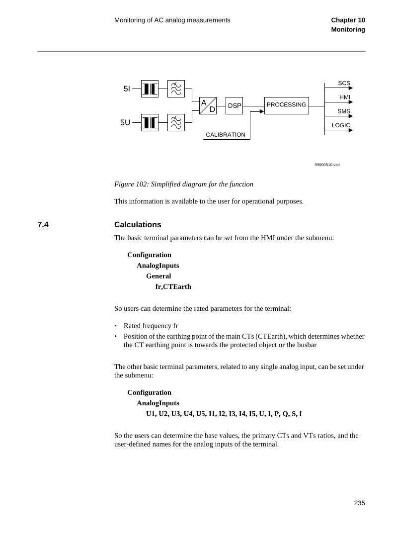
Monitoring of AC analog measurements Chapter 10Monitoring
ther
t under
d the
Figure 102: Simplified diagram for the function
This information is available to the user for operational purposes.
7.4 Calculations
The basic terminal parameters can be set from the HMI under the submenu:
Configuration
AnalogInputs
General
fr,CTEarth
So users can determine the rated parameters for the terminal:
• Rated frequency fr
• Position of the earthing point of the main CTs (CTEarth), which determines whethe CT earthing point is towards the protected object or the busbar
The other basic terminal parameters, related to any single analog input, can be sethe submenu:
Configuration
AnalogInputs
U1, U2, U3, U4, U5, I1, I2, I3, I4, I5, U, I, P, Q, S, f
So the users can determine the base values, the primary CTs and VTs ratios, anuser-defined names for the analog inputs of the terminal.
99000510.vsd
AD DSP
5I
5U
PROCESSING
CALIBRATION
SCS
HMI
SMS
LOGIC
235

Monitoring of AC analog measurements Chapter 10Monitoring
ale
ale
ale
ale
ale
Under U1:
• ac voltage base value for analog input U1: U1b
• voltage transformer input U1 nominal primary to secondary scale value: U1Sc
• Name (of up to 13 characters) of the analog input U1: Name
Under U2:
• ac voltage base value for analog input U2: U2b
• voltage transformer input U2 nominal primary to secondary scale value: U2Sc
• Name (of up to 13 characters) of the analog input U2: Name
Under U3:
• ac voltage base value for analog input U3: U3b
• voltage transformer input U3 nominal primary to secondary scale value: U3Sc
• Name (of up to 13 characters) of the analog input U3: Name
Under U4:
• ac voltage base value for analog input U4: U4b
• voltage transformer input U4 nominal primary to secondary scale value: U4Sc
• Name (of up to 13 characters) of the analog input U4: Name
Under U5:
• ac voltage base value for analog input U5: U5b
• voltage transformer input U5 nominal primary to secondary scale value: U5Sc
• Name (of up to 13 characters) of the analog input U5: Name
Under I1:
• ac current base value for analog input I1: I1b
• current transformer input I1 nominal primary to secondary scale value: I1Scale
• Name (of up to 13 characters) of the analog input I1: Name
Under I2:
236

Monitoring of AC analog measurements Chapter 10Monitoring
• ac current base value for analog input I2: I2b
• current transformer input I2 nominal primary to secondary scale value: I2Scale
• Name (of up to 13 characters) of the analog input I2: Name
Under I3:
• ac current base value for analog input I3: I3b
• current transformer input I3 nominal primary to secondary scale value: I3Scale
• Name (of up to 13 characters) of the analog input I3: Name
Under I4:
• ac current base value for analog input I4: I4b
• current transformer input I4 nominal primary to secondary scale value: I4Scale
• Name (of up to 13 characters) of the analog input I4: Name
Under I5:
• ac current base value for analog input I5: I5b
• current transformer input I5 nominal primary to secondary scale value: I5Scale
• Name (of up to 13 characters) of the analog input I5: Name
Under U:
• Name (of up to 13 characters) of the average voltage U: Name
Under I:
• Name (of up to 13 characters) of the average current I: Name
Under P:
• Name (of up to 13 characters) of the active power P: Name
Under Q:
• Name (of up to 13 characters) of the reactive power Q: Name
237
Monitoring of AC analog measurements Chapter 10Monitoring
on
eters
yster-r each
ed
Under S:
• Name (of up to 13 characters) of the apparent power S: Name
Under f:
• Name (of up to 13 characters) of the frequency value f: Name
The names of the first 10 quantities automatically appears in the REVAL evaluatiprogram for each reported disturbance.
The PST Parameter Setting Tool has to be used in order to set all remaining paramthat are related to different alternating measuring quantities.
In the settings menu it is possible to set all monitoring operating values and the hesis directly in the basic units of the measured quantities for each channel and foquantity:
Settings
DisturbReport
AnalogSignals
The dead-band limits can be set directly in the corresponding units of the observquantity for the:
• Amplitude dead-band supervision (ADBS)
• Integrating dead-band supervision (IDBS)
The IDBS area is defined by the following formula:
(Equation 72)
Where:
IDBS IDeadBReadFreq----------------------------- IDeadB ts⋅= =
238
Monitoring of AC analog measurements Chapter 10Monitoring
The setting value for IDBS is IDeadB, and is expressed in the measuring unit of the monitored quantity (kV, A, MW, Mvar, MVA or Hz). The value is reported if the time integral area is greater than the value IDBS.
If a 0.1 Hz variation in the frequency for 10 minutes (600 s) is the event that should cause the reporting of the frequency monitored value, than the set value for IDeadB is 60 Hz.
The hysteresis can be set under the setting Hysteres.
Alarm and warning thresholds have to be set respectively under the settings HiAlarm (LowAlarm) and HiWarn (LowWarn).
See the Technical reference manual for a list of all the setting parameters.
IDeadB is a set operating value for IDBS in corresponding unit.
ReadFreq is the reading frequency. It has a constant value of 1Hz.
ts = 1/ReadFreq is the time between two samples (fixed to 1s).
Note!
It is important to set the time for periodic reporting and deadband in an optimized wayto minimize the load on the station bus.
239
Monitoring of DC analog measurements Chapter 10Monitoring
ltage ts and nd
cal t cases, direct rtion
uring d
ea-tion cated one tech-
nt lo-
8 Monitoring of DC analog measurements
8.1 Application
Fast, reliable supervision of different analogue quantities is of vital importance during the normal operation of a power system. Operators in the control centres can, for exam-ple:
• Continuously follow active and reactive power flow in the network
• Supervise the busbar voltages
• Check the temperature of power transformers, shunt reactors
• Monitor the gas pressure in circuit breakers
Different measuring methods are available for different quantities. Current and voinstrument transformers provide the basic information on measured phase currenvoltages in different points within the power system. At the same time, currents avoltages serve as the input measuring quantities to power and energy meters.
Different measuring transducers provide information on electrical and non-electrimeasuring quantities such as voltage, current, temperature, and pressure. In mosthe measuring transducers change the values of the measured quantities into thecurrent. The current value usually changes within the specified mA range in propoto the value of the measured quantity.
Further processing of the direct currents obtained on the outputs of different measconverters occurs within different control, protection, and monitoring terminals anwithin the higher hierarchical systems in the secondary power system.
8.2 Functionality
The REx 5xx control, protection and monitoring terminal have a built-in option to msure and further process information from 6 up to 36 different direct current informafrom different measuring transducers. Six independent measuring channels are loon each independent mA input module and the REx 5xx terminals can accept fromup to six independent mA input modules, depending on the case size. Refer to thenical data and ordering particulars for the particular terminal.
Information about the measured quantities is then available to the user on differecations:
240

Monitoring of DC analog measurements Chapter 10Monitoring
y the steps han
bove oc-ll oc-
f a te
ans of ther
-set
Low-
• Locally by means of the local human-machine-interface (HMI)
• Locally by means of a front-connected personal computer (PC)
• Remotely over the LON bus to the station control system (SCS)
• Remotely over the SPA port to the station monitoring system (SMS)
User-defined measuring ranges
The measuring range of different direct current measuring channels is settable buser independent on each other within the range between -25 mA and +25 mA inof 0.01 mA. It is only necessary to select the upper operating limit I_Max higher tthe lower one I_Min.
The measuring channel can have a value of 2 of the whole range I_Max - I_Min athe upper limit I_Max or below the lower limit I_Min, before an out-of-range error curs. This means that with a nominal range of 0-10 mA, no out-of-range event wicur with a value between -0.2 mA and 10.2 mA.
User can this way select for each measuring quantity on each monitored object opower system the most suitable measuring range and this way optimize a complefunctionality together with the characteristics of the used measuring transducer.
Continuous monitoring of the measured quantity
The user can continuously monitor the measured quantity in each channel by mesix built-in operating limits (figure 103). Two of them are defined by the operatingrange selection: I_Max as the upper and I_Min as the lower operating limit. The ofour operating limits operate in two different modes:
• Overfunction, when the measured current exceeds the HiWarn or HiAlarm prevalues
• Underfunction, when the measured current decreases under the LowWarn or Alarm pre-set values
241
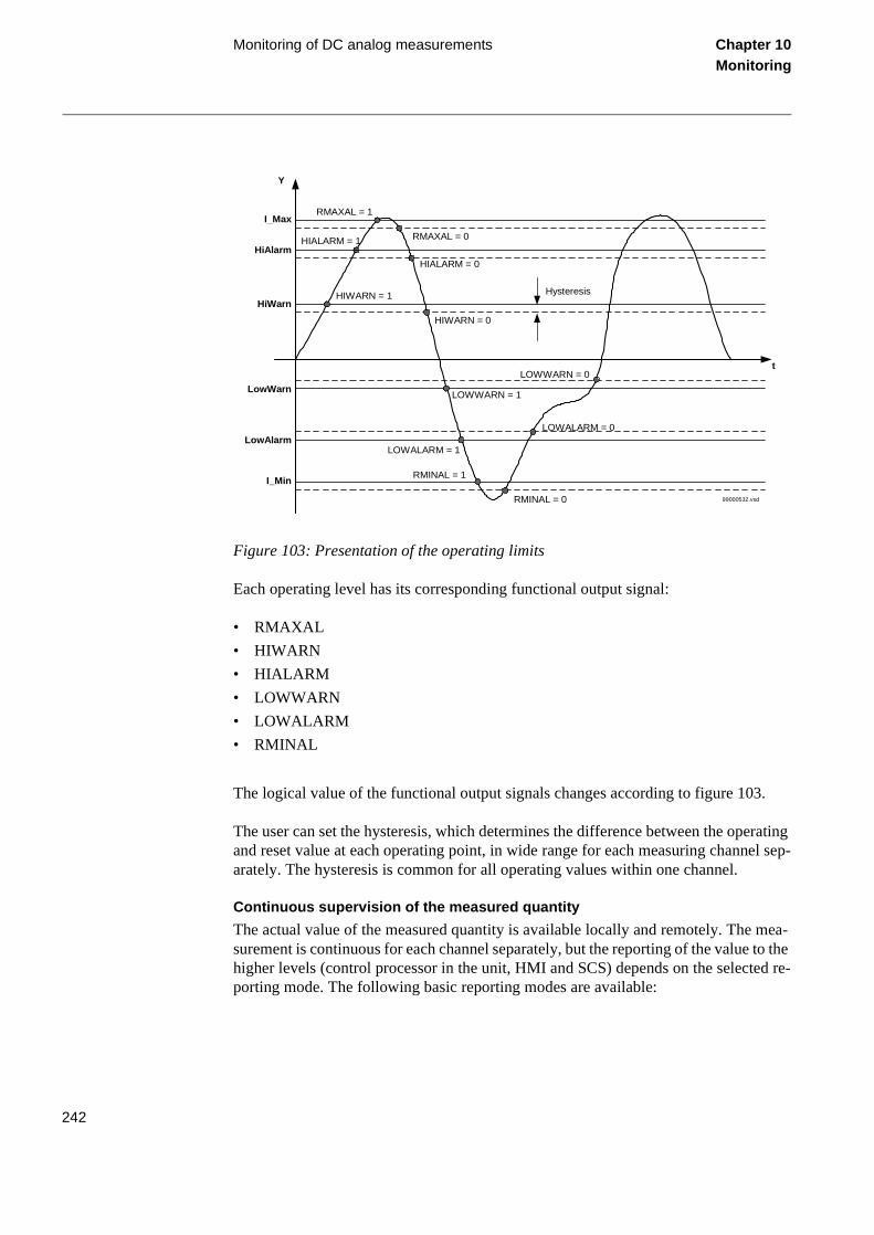
Monitoring of DC analog measurements Chapter 10Monitoring
.
erating el sep-
mea- to the ed re-
Figure 103: Presentation of the operating limits
Each operating level has its corresponding functional output signal:
• RMAXAL
• HIWARN
• HIALARM
• LOWWARN
• LOWALARM
• RMINAL
The logical value of the functional output signals changes according to figure 103
The user can set the hysteresis, which determines the difference between the opand reset value at each operating point, in wide range for each measuring channarately. The hysteresis is common for all operating values within one channel.
Continuous supervision of the measured quantity
The actual value of the measured quantity is available locally and remotely. The surement is continuous for each channel separately, but the reporting of the valuehigher levels (control processor in the unit, HMI and SCS) depends on the selectporting mode. The following basic reporting modes are available:
99000532.vsd
HIWARN = 1
HIALARM = 1
HIWARN = 0
HIALARM = 0
Hysteresis
HiAlarm
HiWarn
LowWarn
LowAlarm
LOWWARN = 1
LOWALARM = 1
LOWALARM = 0
LOWWARN = 0
Y
t
I_MaxRMAXAL = 1
RMAXAL = 0
I_MinRMINAL = 1
RMINAL = 0
242
Monitoring of DC analog measurements Chapter 10Monitoring
/- mple,
e in-c re-
ed at te set-
ore
• Periodic reporting
• Periodic reporting with dead-band supervision in parallel
• Periodic reporting with dead-band supervision in series
• Dead-band reporting
Users can select between two types of dead-band supervision:
• Amplitude dead-band supervision (ADBS).
• Integrating dead-band supervision (IDBS).
Amplitude dead-band supervision
If the changed value —compared to the last reported value— is larger than the +∆Y predefined limits that are set by users, and if this is detected by a new measuring sathen the measuring channel reports the new value to a higher level. This limits thformation flow to a minimum necessary. Figure 104 shows an example of periodiporting with the amplitude dead-band supervision.
The picture is simplified: the process is not continuous but the values are evaluattime intervals depending on the sampling frequency chosen by the user (SampRating).
After the new value is reported, the new +/- ∆Y limits for dead-band are automaticallyset around it. The new value is reported only if the measured quantity changes mthan defined by the new +/- ∆Y set limits.
243

Monitoring of DC analog measurements Chapter 10Monitoring
Figure 104: Amplitude dead-band supervision reporting
Integrating dead-band supervision
The measured value is updated if the time integral of all changes exceeds the pre-set limit (figure 105), where an example of reporting with integrating dead-band supervi-sion is shown. The picture is simplified: the process is not continuous but the values are evaluated at time intervals depending on the sampling frequency chosen by the user (SampRate setting).
The last value reported (Y1 in figure 105) serves as a basic value for further measure-ment. A difference is calculated between the last reported and the newly measured value during new sample and is multiplied by the time increment (discrete integral). The ab-solute values of these products are added until the pre-set value is exceeded. This occurs with the value Y2 that is reported and set as a new base for the following measurements (as well as for the values Y3, Y4 and Y5).
The integrating dead-band supervision is particularly suitable for monitoring signals with low variations that can last for relatively long periods.
99000529.vsd
Y
t
Value Reported(1st)
Value ReportedValue Reported
Y1
Y2
Y3
∆Y∆Y
∆Y∆Y
∆Y∆Y
Value Reported
244

Monitoring of DC analog measurements Chapter 10Monitoring
Figure 105: Reporting with integrating dead-band supervision
Periodic reporting
The user can select the periodic reporting of measured value in time intervals between 1 and 3600 s (setting RepInt). The measuring channel reports the value even if it has not changed for more than the set limits of amplitude or integrating dead-band supervision (figure 106). To disable periodic reporting, set the reporting time interval to 0 s.
Figure 106: Periodic reporting
99000530.vsd
Y
t
Value Reported(1st)
Y1
ValueReported
A1Y2
ValueReported
Y3
Y4
AValueReported
A2
Y5A3
A4A5 A7
A6
ValueReported
A2 >=pre-set value
A1 >=pre-set valueA >=
pre-set value
A3 + A4 + A5 + A6 + A7 >=pre-set value
99000528.vsd
Val
ue 1
Y
t
Val
ue 2
Val
ue 3
Val
ue 4
Value Reported(1st)
Value Reported
Val
ue 5
Value Reported
Y1
Y2
Y5
Value Reported Value Reported
Y3Y4
(*)Set value for t: RepInt
t (*) t (*) t (*) t (*)
245
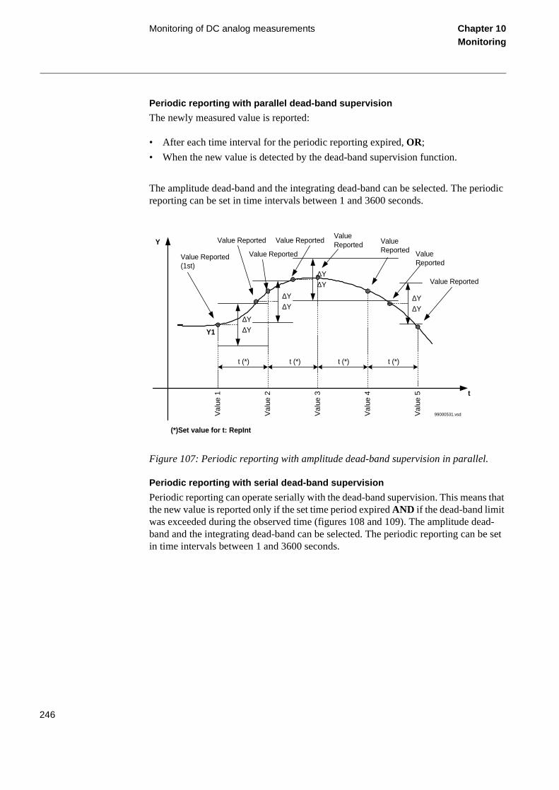
Monitoring of DC analog measurements Chapter 10Monitoring
riodic
s that
ad-be set
Periodic reporting with parallel dead-band supervision
The newly measured value is reported:
• After each time interval for the periodic reporting expired, OR;
• When the new value is detected by the dead-band supervision function.
The amplitude dead-band and the integrating dead-band can be selected. The pereporting can be set in time intervals between 1 and 3600 seconds.
Figure 107: Periodic reporting with amplitude dead-band supervision in parallel.
Periodic reporting with serial dead-band supervision
Periodic reporting can operate serially with the dead-band supervision. This meanthe new value is reported only if the set time period expired AND if the dead-band limit was exceeded during the observed time (figures 108 and 109). The amplitude deband and the integrating dead-band can be selected. The periodic reporting can in time intervals between 1 and 3600 seconds.
99000531.vsdVal
ue 1
Y
t
Val
ue 2
Val
ue 3
Val
ue 4
Value Reported(1st)
Value ReportedValueReported
Val
ue 5
Value Reported
Y1
∆Y∆Y
ValueReported
t (*) t (*) t (*) t (*)
(*)Set value for t: RepInt
Value Reported
∆Y∆Y
Value Reported
∆Y∆Y
ValueReported
∆Y∆Y
246
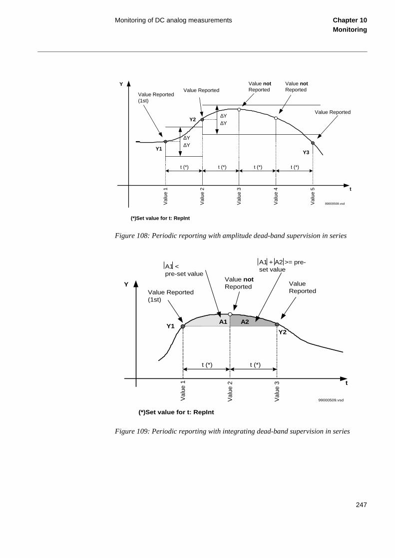
Monitoring of DC analog measurements Chapter 10Monitoring
Figure 108: Periodic reporting with amplitude dead-band supervision in series
Figure 109: Periodic reporting with integrating dead-band supervision in series
99000508.vsdVal
ue 1
Y
t
Val
ue 2
Val
ue 3
Val
ue 4
Value Reported(1st)
Value Reported
∆Y∆Y
Value notReported
Val
ue 5
Value Reported
Y1
Y2
Y3
∆Y∆Y
Value notReported
t (*) t (*) t (*) t (*)
(*)Set value for t: RepInt
99000509.vsd
Y
t
Val
ue 1
Val
ue 2
Val
ue 3
Value Reported(1st)
Value notReported
Y1
ValueReported
A1 A2
Y2
t (*) t (*)
(*)Set value for t: RepInt
A1 <pre-set value
A1 + A2 >= pre-set value
247

Monitoring of DC analog measurements Chapter 10Monitoring
Combination of periodic reportings
The reporting of the new value depends on setting parameters for the dead-band and for the periodic reporting. Table 1 presents the dependence between different settings and the type of reporting for the new value of a measured quantity.
Table 14: Dependence of reporting on different setting parameters:
EnDeadB * EnIDeadB * EnDeadBP * RepInt * Reporting of the new value
Off Off Off 0 No measured values is reported
Off On On t>0 The new measured value is reported
only if the time t period expired and if, during this time, the integrating dead-band limits were exceeded (periodic
reporting with integrating dead-band supervision in series)
On Off On t>0 The new measured value is reported
only if the time t period has expired and if, during this time, the amplitude dead-band limits were exceeded (periodic
reporting with amplitude dead-band supervision in series)
On On On t>0 The new measured value is reported
only if the time t period expired and if at least one of the dead-band limits were exceeded (periodic reporting with
dead-band supervision in series)
Off On Off 0 The new measured value is reported only when the integrated dead-band
limits are exceeded
On Off Off 0 The new measured value is reported only when the amplitude dead-band
limits were exceeded
248
Monitoring of DC analog measurements Chapter 10Monitoring
8.3 Design
The design of the mA input modules follows the design of all REx 5xx-series protec-tion, control, and monitoring terminals that have distributed functionality, where the de-cision levels are placed as closely as possible to the process.
Each independent measuring module contains all necessary circuitry and functionality for measurement of six independent measuring quantities related to the corresponding measured direct currents.
On the accurate input shunt resistor (R), the direct input current (from the measuring converter) is converted into a proportional voltage signal (the voltage drop across the shunt resistor is in proportion to the measured current). Later, the voltage signal is pro-cessed within one differential type of measuring channel (figure 110).
On On Off 0 The new measured value is reported
only if one of the dead-band limits was exceeded
x x Off t>0 The new measured value is updated at least after the time t period expired. If the dead-band supervision is addition-
ally selected, the updating also occurs when the corresponding dead-band limit was exceeded (periodic reporting
with parallel dead-band supervision)
* Please see the setting parameters in the Technical reference manual for further explanation
EnDeadB * EnIDeadB * EnDeadBP * RepInt * Reporting of the new value
249
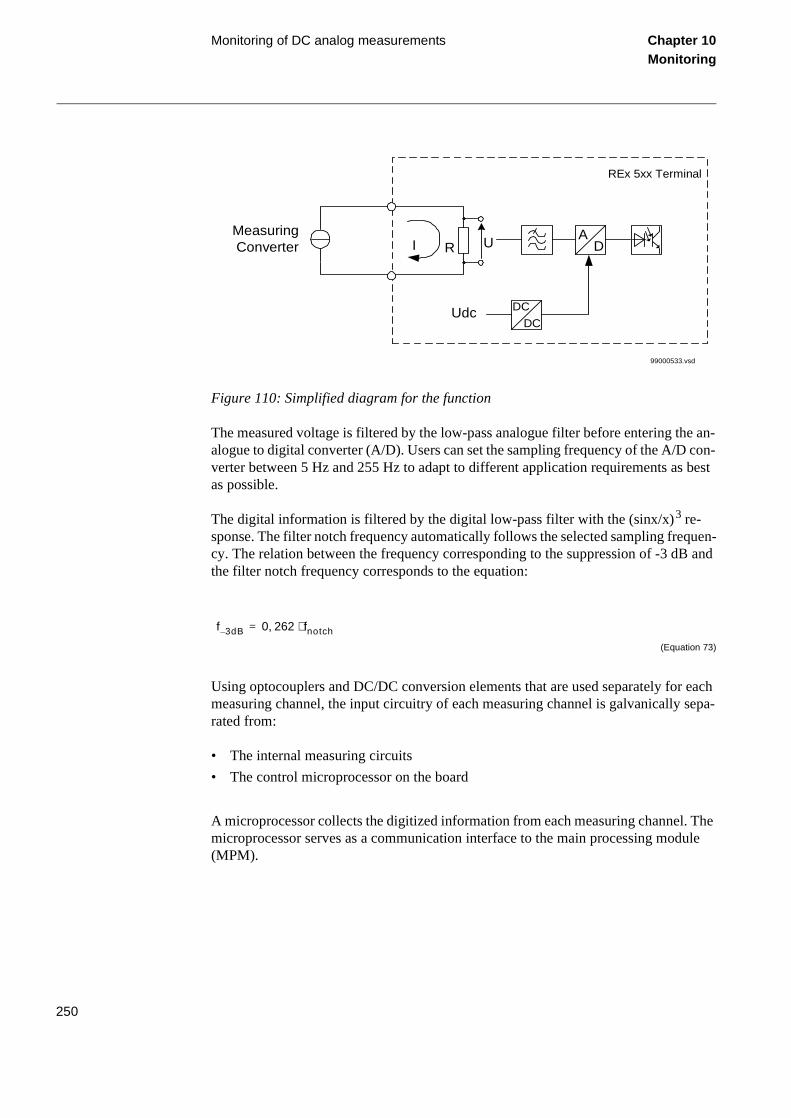
Monitoring of DC analog measurements Chapter 10Monitoring
The ule
Figure 110: Simplified diagram for the function
The measured voltage is filtered by the low-pass analogue filter before entering the an-alogue to digital converter (A/D). Users can set the sampling frequency of the A/D con-verter between 5 Hz and 255 Hz to adapt to different application requirements as best as possible.
The digital information is filtered by the digital low-pass filter with the (sinx/x)3 re-sponse. The filter notch frequency automatically follows the selected sampling frequen-cy. The relation between the frequency corresponding to the suppression of -3 dB and the filter notch frequency corresponds to the equation:
(Equation 73)
Using optocouplers and DC/DC conversion elements that are used separately for each measuring channel, the input circuitry of each measuring channel is galvanically sepa-rated from:
• The internal measuring circuits
• The control microprocessor on the board
A microprocessor collects the digitized information from each measuring channel.microprocessor serves as a communication interface to the main processing mod(MPM).
99000533.vsd
I R UA
D
DC
DCUdc
MeasuringConverter
REx 5xx Terminal
f 3dB– 0 262, fnotch⋅=
250
Monitoring of DC analog measurements Chapter 10Monitoring
o
ess. era-
parts
ts the value
quan-
ly the rs, e
errors
hat are
A of
e cor-sers
range
All processing of the measured signal is performed on the module so that only the min-imum amount of information is necessary to be transmitted to and from the MPM. The measuring module receives information from the MPM on setting and the command pa-rameters; it reports the measured values and additional information—according tneeds and values of different parameters.
Each measuring channel is calibrated very accurately during the production procThe continuous internal zero offset and full-scale calibration during the normal option is performed by the A/D converter. The calibration covers almost all analogue of the A/D conversion, but neglects the shunt resistance.
Each measuring channel has built in a zero-value supervision, which greatly rejecnoise generated by the measuring transducers and other external equipment. Theof the measured input current is reported equal to zero (0) if the measured primarytity does not exceed +/-0.5% of the maximum measuring range.
The complete measuring module is equipped with advanced self-supervision. Onoutermost analogue circuits cannot be monitored. The A/D converter, optocoupledigital circuitry, and DC/DC converters, are all supervised on the module. Over thCAN bus, the measuring module sends a message to the MPM for any detectedon the supervised circuitry.
8.4 Calculations
The PST Parameter Setting Tool has to be used in order to set all the parameters trelated to different DC analogue quantities.
Users can set the 13 character name for each measuring channel.
All the monitoring operating values and the hysteresis can be set directly in the mthe measured input currents from the measuring transducers.
The measured quantities can be displayed locally and/or remotely according to thresponding modules that are separately set for each measuring channel by the u(five characters).
The relation between the measured quantity in the power system and the settingof the direct current measuring channel corresponds to this equation:
(Equation 74)
Value ValueMin I IMin–( ) ValueMax ValueMin–IMax IMin–
--------------------------------------------------------------⋅+=
251

Monitoring of DC analog measurements Chapter 10Monitoring
Where:
Figure 111 shows the relationship between the direct mA current I and the actual value of the primary measured quantity, Value.
I_Min is the set value for the minimum operating current of a channel in mA.
I_Max is the set value for the maximum operating current of a channel in mA.
ValueMin is the value of the primary measuring quantity corresponding to the set value of
minimum operating current of a channel, I_Min.
ValueMax is the value of the primary measuring quantity corresponding to the set value of maximum operating current of a channel, I_Max.
Value is the actual value of the primary measured quantity.
252
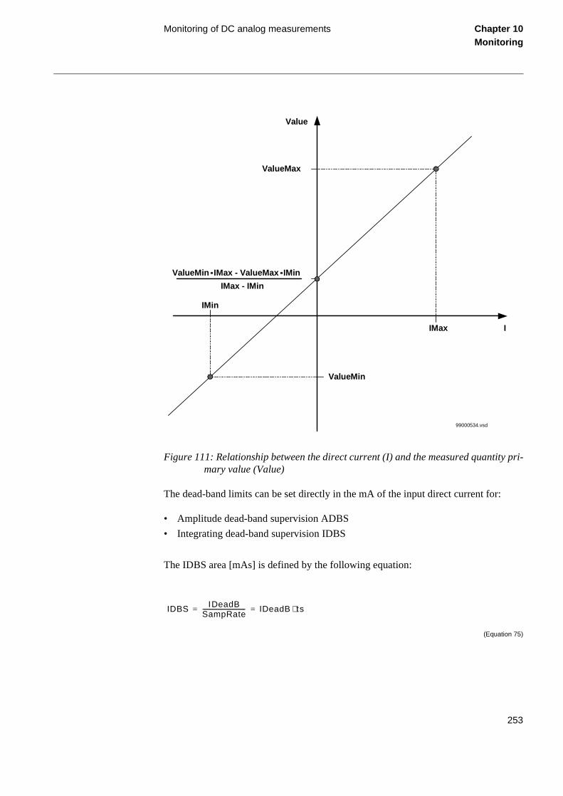
Monitoring of DC analog measurements Chapter 10Monitoring
Figure 111: Relationship between the direct current (I) and the measured quantity pri-mary value (Value)
The dead-band limits can be set directly in the mA of the input direct current for:
• Amplitude dead-band supervision ADBS
• Integrating dead-band supervision IDBS
The IDBS area [mAs] is defined by the following equation:
(Equation 75)
Value
IMin
ValueMin
ValueMin IMax - ValueMax IMin
IMax - IMin
IMax
ValueMax
I
99000534.vsd
IDBS IDeadBSampRate------------------------------ IDeadB ts⋅= =
253
Monitoring of DC analog measurements Chapter 10Monitoring
If a 0.1 mA variation in the monitored quantity for 10 minutes (600 s) is the event that should cause the trigger of the IDBS monitoring (reporting of the value because of IDBS threshold operation) and the sampling frequency (SampRate) of the monitored quantity is 5 Hz, than the set value for IDBS (IDeadB) will be 300 mA:
(Equation 76)
(Equation 77)
The polarity of connected direct current input signal can be changed by setting the ChSign to On or Off. This way it is possible to compensate by setting the possible wrong connection of the direct current leads between the measuring converter and the input terminals of the REx 5xx series unit.
The setting table lists all setting parameters with additional explanation.
where:
IDeadB is the set value of the current level for IDBS in mA.
SampRate is the sampling rate (frequency) set value, in Hz.
ts = 1/SampRate is the time between two samples in s.
IDBS 0.1 600⋅ 60 mA s ][= =
IDeadB IDBS SampRate⋅ 60 5⋅ 300 mA ][= = =
Note:
It is important to set the time for periodic reporting and deadband in an optimized wayto minimize the load on the station bus.
254

About this chapter Chapter 11Metering
Chapter 11 Metering
About this chapter
This chapter describes the metering functions.
255

Pulse counter logic (PC) Chapter 11Metering
1 Pulse counter logic (PC)
1.1 Application
The pulse counter function provides the Substation Automation system with the number of pulses, which have been accumulated in the REx 5xx terminal during a defined pe-riod of time, for calculation of, for example, energy values. The pulses are captured on the Binary Input Module (BIM) that is read by the pulse counter function. The number of pulses in the counter is then reported via LON to the station HMI or read via SPA as a service value.
The normal use for this function is the counting of energy pulses for kWh and kvarh in both directions from external energy meters. Up to 12 binary inputs in a REx 5xx can be used for this purpose with a frequency of up to 40 Hz.
1.2 Functionality
The registration of pulses is done for positive transitions (0->1) on one of the 16 binary input channels located on the Binary Input Module (BIM). Pulse counter values are read from the station HMI with predefined cyclicity without reset, and an event is created.
The integration time period can be set in the range from 30 seconds to 60 minutes and is synchronised with absolute system time. That means, a cycle time of one minute will generate a pulse counter reading every full minute. Interrogation of additional pulse counter values can be done with a command (intermediate reading) for a single counter. All active counters can also be read by the LON General Interrogation command (GI).
The pulse counter in REx 5xx supports unidirectional incremental counters. That means only positive values are possible. The counter uses a 32 bit format, that is, the reported value is a 32-bit, signed integer with a range 0...+2147483647. The counter is reset at initialisation of the terminal or by turning the pulse counter operation parameter Off/On.
The reported value to station HMI over the LON bus contains Identity, Value, Time, and Pulse Counter Quality. The Pulse Counter Quality consists of:
• Invalid (board hardware error or configuration error)
• Wrapped around
• Blocked
• Adjusted
256
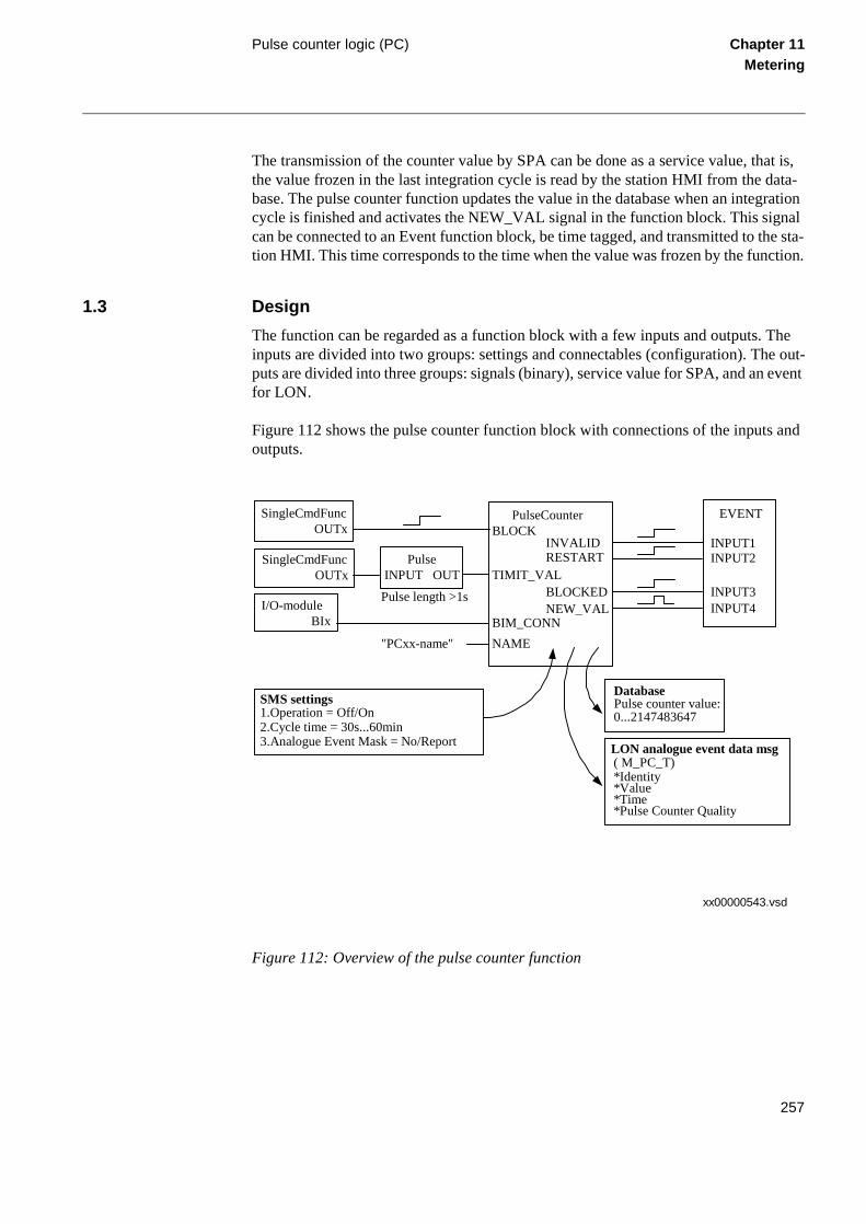
Pulse counter logic (PC) Chapter 11Metering
The transmission of the counter value by SPA can be done as a service value, that is, the value frozen in the last integration cycle is read by the station HMI from the data-base. The pulse counter function updates the value in the database when an integration cycle is finished and activates the NEW_VAL signal in the function block. This signal can be connected to an Event function block, be time tagged, and transmitted to the sta-tion HMI. This time corresponds to the time when the value was frozen by the function.
1.3 Design
The function can be regarded as a function block with a few inputs and outputs. The inputs are divided into two groups: settings and connectables (configuration). The out-puts are divided into three groups: signals (binary), service value for SPA, and an event for LON.
Figure 112 shows the pulse counter function block with connections of the inputs and outputs.
Figure 112: Overview of the pulse counter function
xx00000543.vsd
PulseCounterBLOCK
TIMIT_VAL
BIM_CONN
NAME
PulseINPUT OUT
DatabasePulse counter value:0...2147483647
SMS settings1.Operation = Off/On2.Cycle time = 30s...60min3.Analogue Event Mask = No/Report LON analogue event data msg
( M_PC_T)*Identity*Value*Time*Pulse Counter Quality
SingleCmdFunc OUTx
SingleCmdFunc OUTx
I/O-module BIx
"PCxx-name"
Pulse length >1s
INVALIDRESTART
BLOCKEDNEW_VAL
INPUT1INPUT2
INPUT3INPUT4
EVENT
257
Pulse counter logic (PC) Chapter 11Metering
up-
r) in :
n /
The BLOCK and TMIT_VAL inputs can be connected to Single Command blocks, which are intended to be controlled either from the station HMI or/and the local HMI. As long as the BLOCK signal is set, the pulse counter is blocked. The signal connected to TMIT_VAL performs one additional reading per positive flank. The signal must be a pulse with a length >1 second.
The BIM_CONN input is connected to the used input of the function block for the Bi-nary Input Module (BIM). If BIM_CONN is connected to another function block, the INVALID signal is activated to indicate the configuration error.
The NAME input is used for a user-defined name with up to 19 characters.
Each pulse counter function block has four output signals: INVALID, RESTART, BLOCKED, and NEW_VAL. These signals can be connected to an Event function block for event recording.
The INVALID signal is a steady signal and is set if the Binary Input Module, where the pulse counter input is located, fails or has wrong configuration.
The RESTART signal is a steady signal and is set when the reported value does not comprise a complete integration cycle. That is, in the first message after terminal start-up, in the first message after deblocking, and after the counter has wrapped around dur-ing last integration cycle.
The BLOCKED signal is a steady signal and is set when the counter is blocked. There are two reasons why the counter is blocked:
• The BLOCK input is set, or
• The Binary Input Module, where the counter input is situated, is inoperative.
The NEW_VAL signal is a pulse signal. The signal is set if the counter value wasdated since last report.
1.4 Calculations
1.4.1 Setting
From the PST Parameter Setting Tool under SETTINGS/PC01-12 (Pulse Countethe terminal tree, these parameters can be set individually for each pulse counter
• Operation = Off/On
• Cycle Time = 30s / 1min / 1min30s / 2min / 2min30s / 3min / 4min / 5min / 6mi7min30s / 10min / 12min / 15min / 20min / 30min / 60min.
258
Pulse counter logic (PC) Chapter 11Metering
ade
he n
t os-s re-
ase
Under EVENT MASKS/Analogue events/Pulse Counter in PST, the reporting of the analogue events can be masked:
• Event Mask = No Events/Report Events
The configuration of the inputs and outputs of the pulse counter function block is mby the CAP 531 configuration tool.
On the Binary Input Module, the debounce filter time is fixed set to 5 ms, that is, tcounter suppresses pulses with a pulse length less than 5 ms. The input oscillatioblocking frequency is preset to 40 Hz. That means that the counter finds the inpucillating if the input frequency is greater than 40 Hz. The oscillation suppression ileased at 30 Hz. From the PST under CONFIGURATION/Binary I/O-modules/Oscillation in the terminal tree and from the local HMI, the values for blocking/releof the oscillation can be changed.
Note!
The setting is common for all channels on a Binary Input Module, that is, if changes ofthe limits are made for inputs not connected to the pulse counter, the setting also influ-ences the inputs on the same board used for pulse counting.
259

Pulse counter logic (PC) Chapter 11Metering
260
About this chapter Chapter 12Data communication
Chapter 12 Data communication
About this chapter
This chapter describes the data communication and the associated hardware.
261
Remote end data communication Chapter 12Data communication
ork at tion
r if ercon-rotec-
ue to uip-X20) th ions , hort
1 Remote end data communication
1.1 Application
General
The hardware communication modules (or modems) for the Remote end data commu-nication are available in basically three different versions:
• for optical communication
• for short range pilot wire communication
• for galvanic connection to communication equipment according to ITU (formerCCITT) and EIA interface standards.
All systems are designed to be able to work at 64 kbit/s. Some of them can also wNorth American standard of 56 kbit/s. This is especially pointed out in the descripunder each module.
If the protection terminal is located at a long distance (>100 m for V.36, X.21 andRS530 and >10m for G.703) from the communication equipment or multiplexer othe cables run through a noisy area, optical communication should be used to intnect the protection terminal and the communication equipment. In this case the ption terminal contains module used for optical fibre communication and a suitableoptical to electrical converter is installed close to the communication equipment dthe fact that there exists no standard for optical connections to communication eqment. The optical-to-electrical converters that can be used are FOX6Plus (and FOfrom ABB and 21-15xx or 21-16xx from FIBERDATA. The FOX6Plus together wioptical fibre modem supports the G.703 co-directional interfacing and with restrictfor X.21 and V.36. 21-15xx supports V.35 and V.36 while 21-16xx supports X.21G.703 and RS530 co-directional and contra-directional. For 21-15xx and 21-16xx srange optical fibre modem is needed.
NOTE!
When using galvanic connection between protection terminal and communicationequipment or point to point galvanic connection between two protection terminals it isessential that the cable installation is carefully done. See Installation and commission-ing manual for further information.
262

Remote end data communication Chapter 12Data communication
6 bits. essage
Optical connection of multiplexer is only possible if the multiplexer is of type FOX6Plus or FOX20 from ABB. The terminal can then be connected optically to the multiplexer, provided the protection is equipped with the optical fibre modem , not the short range fibre optical modem, and the FOX is equipped with an Optical Terminal Module of type N3BT.
1.2 Design
The Remote end data communication consists of two parts, one software part that han-dles the message structure, packing different pieces together, activate sending of the messages, unpacking received messages etc, and one hardware part forming the inter-face against external communication equipments. The hardware part, or built-in mo-dems, can have either galvanic or optical connection. To ensure compatibility with a wide range of communication equipment and media, the terminal is designed to work within the signalling bandwidth of a standard CCITT PCM channel at 64 kbits/s. To en-able the use in North American EIA PCM systems working at 56 kbits/s, some of the interfacing modules can be adapted to this bit rate.
The message is based on the HDLC protocol. This is a protocol for the flow manage-ment of the information on a data communication link that is widely used. The basic information unit on an HDLC link is a frame. A frame consists of:
• start (or opening) flag
• address and control fields (if included)
• data to be transmitted
• CRC word
• end (or closing) flag.
The start and stop flags are 8 bit each and the Cyclic Redundancy Check (CRC) 1The data field differs if between a message sent from a slave to a master and a msent from a master to a slave. The principle design is according to figure 113.
Figure 113: Data message structure
en01000134.vsd
Startflag
Information CRCStopflag
8 bits n x 16 bits 8 bits16 bits
263
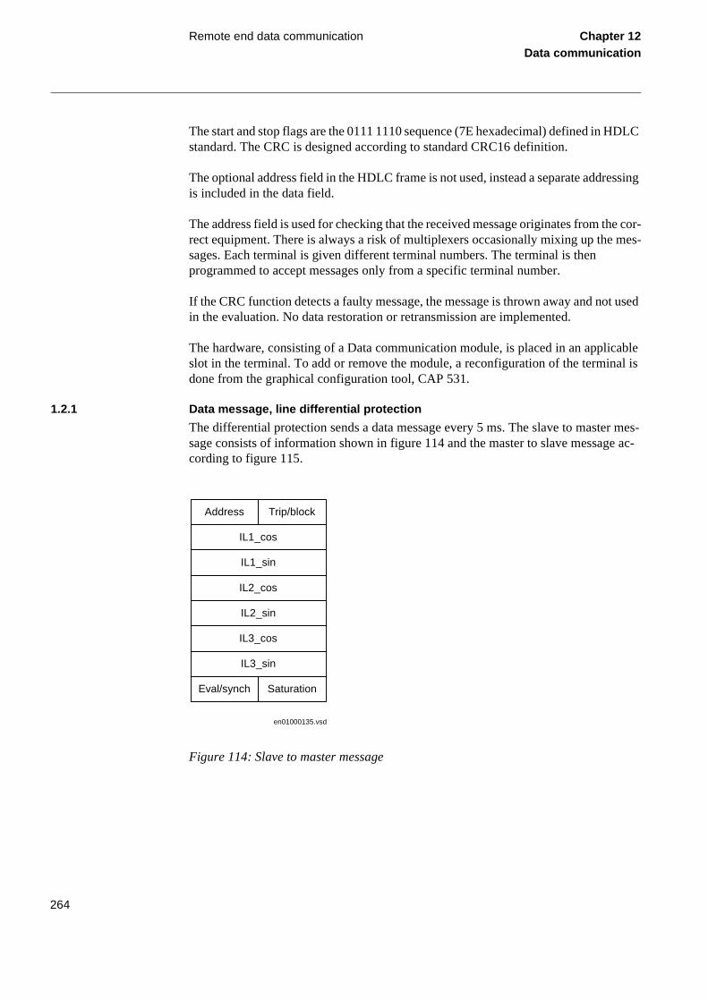
Remote end data communication Chapter 12Data communication
The start and stop flags are the 0111 1110 sequence (7E hexadecimal) defined in HDLC standard. The CRC is designed according to standard CRC16 definition.
The optional address field in the HDLC frame is not used, instead a separate addressing is included in the data field.
The address field is used for checking that the received message originates from the cor-rect equipment. There is always a risk of multiplexers occasionally mixing up the mes-sages. Each terminal is given different terminal numbers. The terminal is then programmed to accept messages only from a specific terminal number.
If the CRC function detects a faulty message, the message is thrown away and not used in the evaluation. No data restoration or retransmission are implemented.
The hardware, consisting of a Data communication module, is placed in an applicable slot in the terminal. To add or remove the module, a reconfiguration of the terminal is done from the graphical configuration tool, CAP 531.
1.2.1 Data message, line differential protection
The differential protection sends a data message every 5 ms. The slave to master mes-sage consists of information shown in figure 114 and the master to slave message ac-cording to figure 115.
Figure 114: Slave to master message
en01000135.vsd
Address Trip/block
IL1_cos
IL1_sin
IL2_cos
IL2_sin
IL3_cos
IL3_sin
Eval/synch Saturation
264
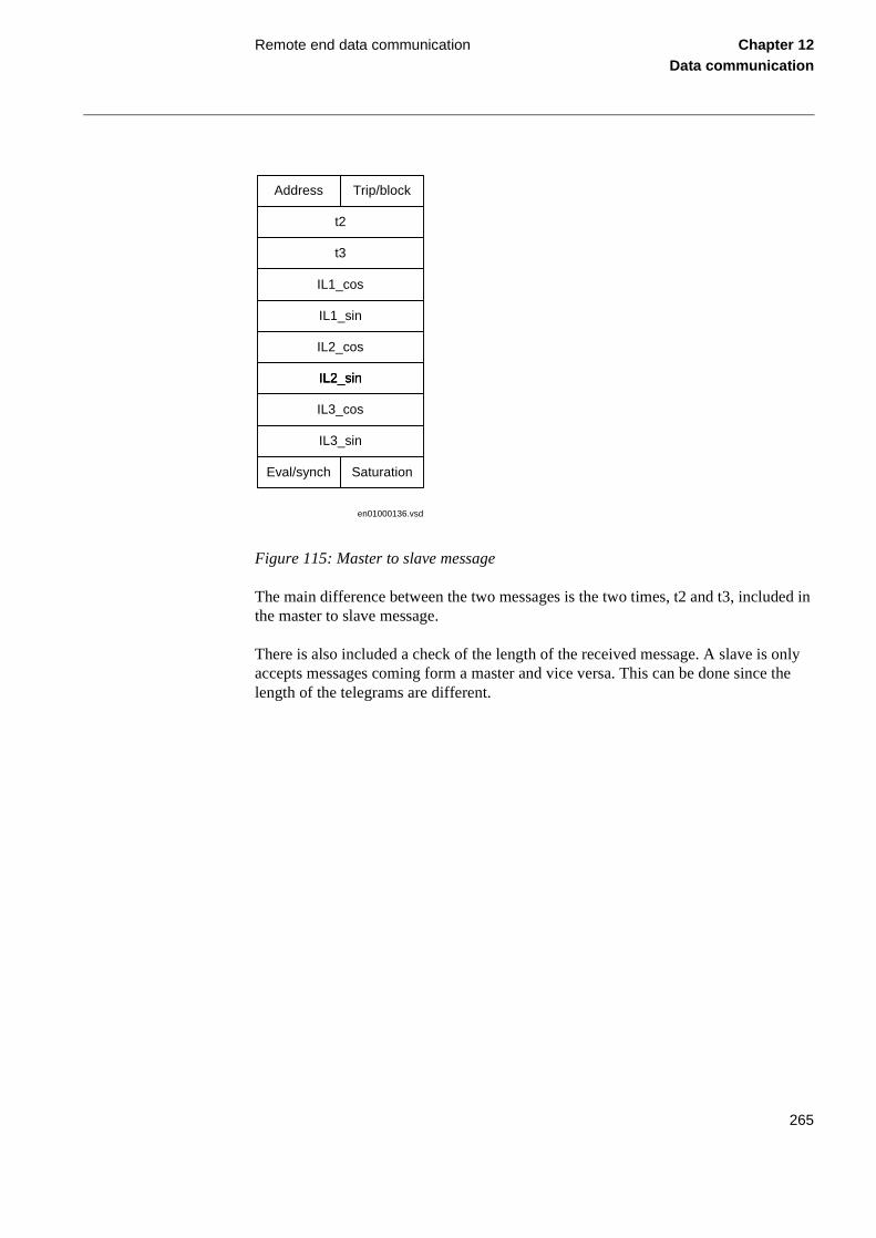
Remote end data communication Chapter 12Data communication
Figure 115: Master to slave message
The main difference between the two messages is the two times, t2 and t3, included in the master to slave message.
There is also included a check of the length of the received message. A slave is only accepts messages coming form a master and vice versa. This can be done since the length of the telegrams are different.
en01000136.vsd
Address Trip/block
t2
t3
IL1_cos
IL1_sin
IL2_cos
IL2_sin
Eval/synch Saturation
IL2_sinIL2_sin
IL3_cos
IL3_sin
265

Optical fibre communication module Chapter 12Data communication
2 Optical fibre communication module
2.1 Application
Optical fibre modem
This module is designed for point to point optical communication, see figure 116, but can also be used for direct optical communication to a multiplexer of type FOX6Plus or FOX20, see figure 117 from ABB, provided it is equipped with an Optical Terminal Module of type N3BT. The FOX6Plus can also be used as an optical to electrical con-verter supporting the G.703 co-directional interfacing according to ITU (former CCITT), see figure 118. FOX6Plus can also in some cases be used for X.21 and V.36 interface but special attention must be paid to how to connect the signal. Used as an op-tical to electrical converter the FOX6Plus only supports 64 kbit/s data transmission.
Figure 116: Dedicated link, opticalfibre connection.
Figure 117: Multiplexed link, optical fibre connection.
xx00000536.vsd
REx5xx
Opticalfibres
<30km
REx5xx
xx00000538.vsd
REx5xx
Opticalfibres
MUX
FOX 20
otherusers
to theother end
<30km
266

Optical fibre communication module Chapter 12Data communication
Figure 118: Multiplexed link, fibre optical-galvanic connection with FOX6Plus
2.2 Design
The optical communication module is designed to work with both 9/125 µm single-mode fibres and 50/125 or 62,5/125 µm multimode fibres at 1300 nm wavelength. The connectors are of type FC-PC (SM) or FC (MM) respectively. Two different levels of optical output power are used to cover distances from 0 to approximately 30 km. The leverl of optical power is selected with a setting. The attenation fibres is normally ap-proximately 0.8 dB/km for multimode and 0.4 dB/km for single-mode. Additional at-tenuation due to installation can be estimated to be 0.2dB/km for multimode and 0.1 dB/km for single-mode fibres. For single-mode fibre and high output power this results in a maximum distance of 32km.
xx00000535.vsd
FOX 6Plus
REx5xx
Opticalfibres
MUX
GalvanicG.703
otherusers
to theother end
<30km
267
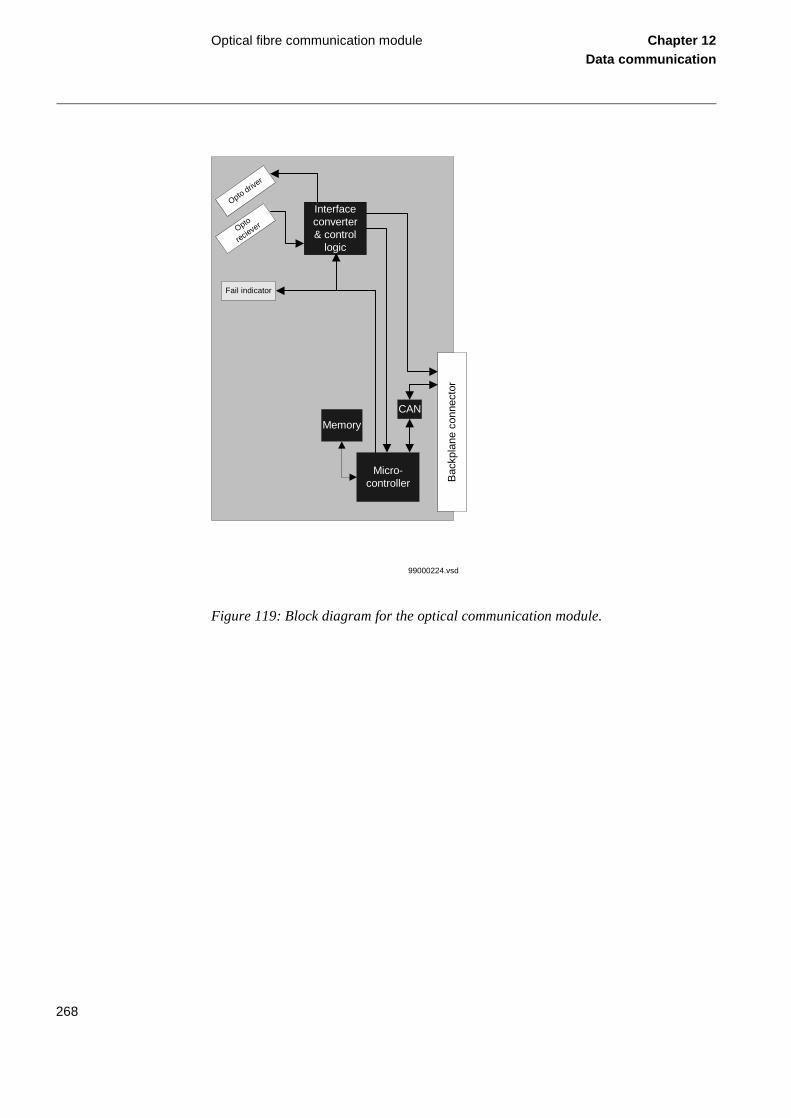
Optical fibre communication module Chapter 12Data communication
Figure 119: Block diagram for the optical communication module.
Interfaceconverter& control
logic
Micro-controller
Memory
CAN
Fail indicator
Opto
reciever
Opto driver
Bac
kpla
ne c
onne
ctor
99000224.vsd
268

Galvanic data communication module Chapter 12Data communication
3 Galvanic data communication module
3.1 Application
Interface modules for V.36, X.21 and RS530
These interface modules are intended for connection to commercially available com-munication equipments or multiplexers and can be used both with 56 and 64 kbit/s data transmission.
Since the protection communicates continuously, a permanent communication circuit is required. Consequently, the call control and handshaking features specified for some interfacing recommendations are not provided.
Even if the standard claims that the reach for these interfaces are up to 1 km at 64 kbit/s it is not recommended to use that distance for protection purposes where the commu-nication has to be reliable also under primary power system faults. This is due to the low level of the communication signals which gives low margin between signal and noise. If the protection terminal is in the same building as the multiplexing equipment and the environment is relatively free from noise, the protection terminal may be con-nected directly to the multiplexer via shielded and properly earthed cables with twisted pairs for distances less than 100 m.
Modules are available for the following interface recommendations, specifying the in-terconnection of the digital equipment to a PCM multiplexer:
• V.35/36 co-directional galvanic interface
• V.35/36 contra-directional galvanic interface
• X.21 galvanic interface
• RS530/422 co-directional galvanic interface
• RS530/422 contra-directional galvanic interface
Note!
Due to problems of timing co-directional operation for V.35/36 and RS530 is only rec-ommended to be used for direct back-to-back operation, for example during laboratorytesting!
269

Galvanic data communication module Chapter 12Data communication
Figure 120: Multiplexed link, galvanic connection
3.2 Design
Figure 121: Block diagram for the galvanic communication module
xx00000539.vsd
REx5xx
GalvanicV.35, V.36,X.21, RS530
56/64 kbt/s
otherusers
to theother end
<100m
MUX
Micro-controller
Memory
CAN
Opt
o is
olat
ion
DC/DC
Trans-ceivers
Pro
cess
con
nect
or X
3P
roce
ss c
onne
ctor
X2
Bac
kpla
ne c
onne
ctor
99000519.vsd
270
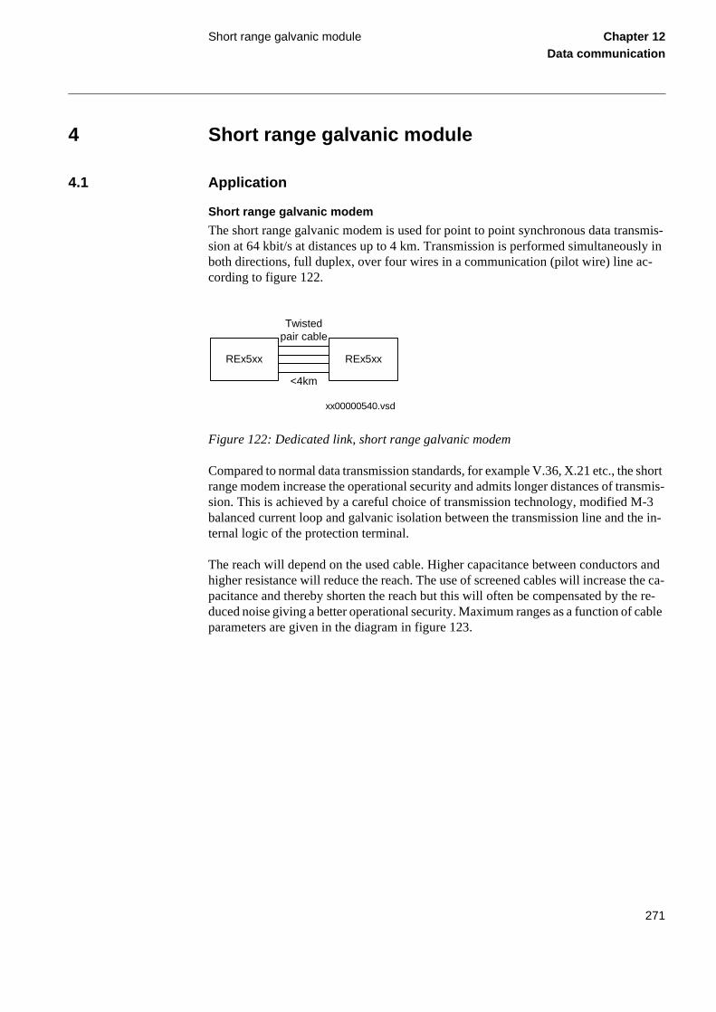
Short range galvanic module Chapter 12Data communication
4 Short range galvanic module
4.1 Application
Short range galvanic modem
The short range galvanic modem is used for point to point synchronous data transmis-sion at 64 kbit/s at distances up to 4 km. Transmission is performed simultaneously in both directions, full duplex, over four wires in a communication (pilot wire) line ac-cording to figure 122.
Figure 122: Dedicated link, short range galvanic modem
Compared to normal data transmission standards, for example V.36, X.21 etc., the short range modem increase the operational security and admits longer distances of transmis-sion. This is achieved by a careful choice of transmission technology, modified M-3 balanced current loop and galvanic isolation between the transmission line and the in-ternal logic of the protection terminal.
The reach will depend on the used cable. Higher capacitance between conductors and higher resistance will reduce the reach. The use of screened cables will increase the ca-pacitance and thereby shorten the reach but this will often be compensated by the re-duced noise giving a better operational security. Maximum ranges as a function of cable parameters are given in the diagram in figure 123.
xx00000540.vsd
REx5xx
<4km
REx5xx
Twistedpair cable
271
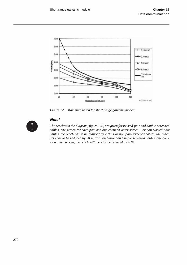
Short range galvanic module Chapter 12Data communication
Figure 123: Maximum reach for short range galvanic modem
Capacitancelimit
Note!
The reaches in the diagram, figure 123, are given for twisted-pair and double-screenedcables, one screen for each pair and one common outer screen. For non twisted-paircables, the reach has to be reduced by 20%. For non pair-screened cables, the reachalso has to be reduced by 20%. For non twisted and single screened cables, one com-mon outer screen, the reach will therefor be reduced by 40%.
272
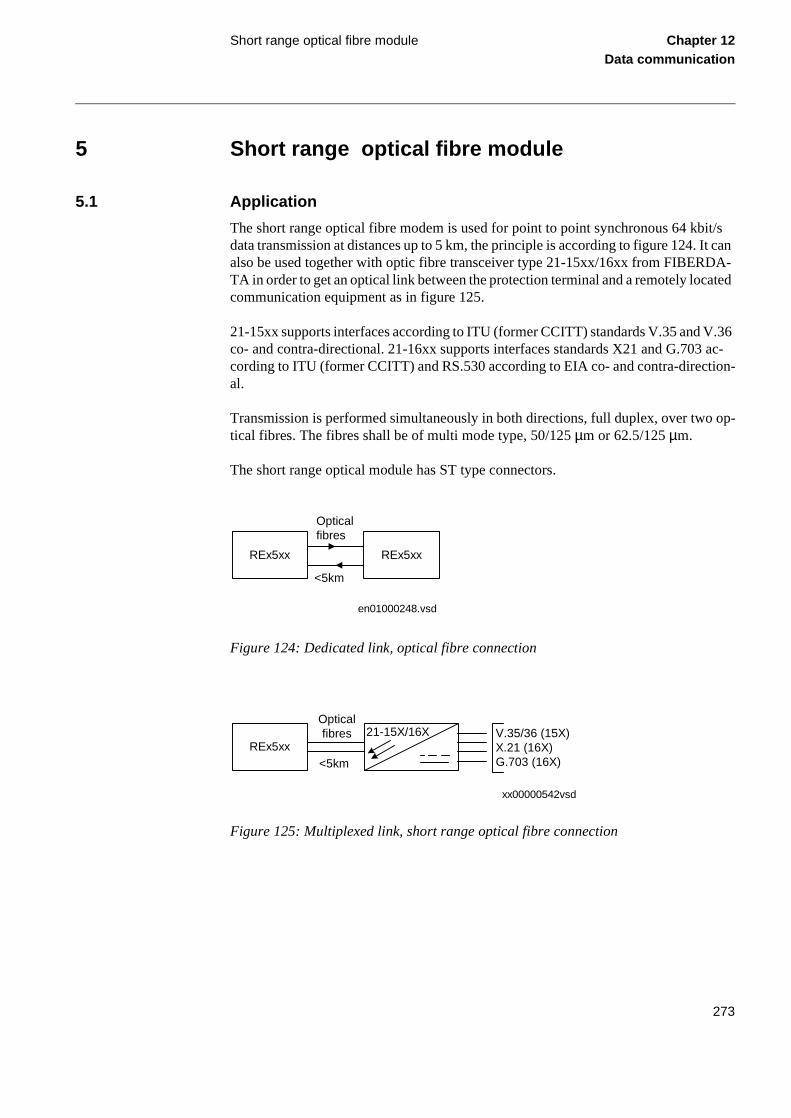
Short range optical fibre module Chapter 12Data communication
5 Short range optical fibre module
5.1 Application
The short range optical fibre modem is used for point to point synchronous 64 kbit/s data transmission at distances up to 5 km, the principle is according to figure 124. It can also be used together with optic fibre transceiver type 21-15xx/16xx from FIBERDA-TA in order to get an optical link between the protection terminal and a remotely located communication equipment as in figure 125.
21-15xx supports interfaces according to ITU (former CCITT) standards V.35 and V.36 co- and contra-directional. 21-16xx supports interfaces standards X21 and G.703 ac-cording to ITU (former CCITT) and RS.530 according to EIA co- and contra-direction-al.
Transmission is performed simultaneously in both directions, full duplex, over two op-tical fibres. The fibres shall be of multi mode type, 50/125 µm or 62.5/125 µm.
The short range optical module has ST type connectors.
Figure 124: Dedicated link, optical fibre connection
Figure 125: Multiplexed link, short range optical fibre connection
en01000248.vsd
REx5xx
Opticalfibres
<5km
REx5xx
xx00000542vsd
REx5xx<5km
Opticalfibres 21-15X/16X V.35/36 (15X)
X.21 (16X)G.703 (16X)
273

Short range optical fibre module Chapter 12Data communication
The reach will depend on the properties of the used optical fibre. In the optical budget has also to be accounted for losses in splices, connectors and also ageing of the cable. The connection to the protection terminal shall not be accounted for in the optical bud-get. 15 dB optical budget gives up to 5 km reach under normal conditions.
274
G.703 module Chapter 12Data communication
6 G.703 module
6.1 Application
Interface modules for G.703 co-directional
This interface module is intended for connection to commercially available communi-cation equipments or multiplexers with G.703 interface. It can only be used with trans-mission rate of 64 kbit/s. Furthermore it only supports co-directional operation. Contra-directional and centralised clock are not supported.
Even if the standard claims that the reach can be rather long at 64 kbit/s, it is not rec-ommended to use this for protection purposes where the communication has to be reli-able also under primary power system faults. This is due to the low level of the communication, signals only 1 V, which gives low margin between signal and noise. If the protection and the communication equipment are located in the same room and the environment is free of noise, the protection terminal may be connected directly to the multiplexer via shielded and properly earthed cables with twisted pairs, same as shown in figure for V.36 etc, for distances up to 10 m.
275
Carrier module Chapter 12Data communication
.
7 Carrier module
7.1 Application
Use the carrier module with the appropriate galvanic or optical communication sub-module for short range communication of binary signals. Use the optical communica-tion module when connecting a FIBERDATA 21-15X or FIBERDATA 21-16X optical-to-electric modem. The 21-15X model supports V.35 and V.36 standards, and the 21-16X model X.21, RS530 or G.703 standards.
7.2 Design
The carrier module is used to connect a communication sub-module to the platform. It adds the CAN-communication and the interface to the rest of the platform. By this the capability to transfer binary signals between for example two distance protection units is added.
The following three types of sub-modules can be added to the carrier module:
• Short range galvanic communication module
• Short range optical communication module
• G.703 communication module
The carrier module senses the type of sub-module via one of the two connectors
276

Carrier module Chapter 12Data communication
Figure 126: Block diagram for the carrier module.
Micro-controllerMemory
CAN
Sub-module
Bac
kpla
ne c
onne
ctor
99000520.vsd
277
Serial communication Chapter 12Data communication
8 Serial communication
8.1 Application
The serial communication can be used for different purposes, which enable better ac-cess to the information stored in the terminals. The serial communication is also used for communication directly between terminals (bay-to-bay communication).
The serial communication can be used with a station monitoring system (SMS) or with a substation control system (SCS). Normally, SPA communication is used for SMS and SCS; LON communication is used for SCS. Additionally, LON communication can also be used for SMS 510. SPA communication is also applied when using the front communication port, but for this purpose, no special serial communication function is required in the terminal. Only the software in the PC and a special cable for front con-nection is needed.
The rear SPA-port can alternatively be set up for IEC 60870-5-103 communication. IEC 60870-5-103 is a standard protocol for protection functions.
278
Serial communication, SPA Chapter 12Data communication
9 Serial communication, SPA
9.1 Application
The SPA communication is mainly used for SMS. It can include different numerical re-lays/terminals with remote communication possibilities. Connection to a personal com-puter (PC) can be made directly (if the PC is located in the substation) or by telephone modem through a telephone network with CCITT characteristics.
Figure 127: Example of SPA communication structure for a station monitoring system
9.2 Functionality
The SPA protocol V2.5 is an ASCII-based protocol for serial communication. The com-munication is based on a master-slave principle, where the terminal is a slave and the PC is the master. Only one master can be applied on each optic fibre loop. A program is needed in the master computer for interpretation of the SPA-bus codes and for trans-lation of the settings sent to the terminal.
9.3 Design
When communicating locally with a Personal Computer (PC) in the station, using the rear SPA port, the only hardware needed for a station monitoring system is:
• Optical fibres
• Opto/electrical converter fo the PC
• PC
REL 5xx*2.3
REB 551*2.3
REC 561*2.3
(Minute pulsefrom station clock)
Telephonemodem
Telephonemodem
SMS 510CAP 535REVAL
Opto/electricalconverter
SPA busOptical fibreloop
en01000080.vsd
279
Serial communication, SPA Chapter 12Data communication
ce to
spe-
ce to
n of
col to
s to
num-l for all
n at:
When communicating remotely with a PC using the rear SPA port, the same hardware is needed plus telephone modems.
The software needed in the PC, either local or remote, is:
• CAP 535 (Ver. 1.0 or higher) for configuration and parameter setting
• SMS 510 (Ver 1.0 or higher) for reading of disturbance records, events, distanfault and trip value settings
• REVAL (Ver 2.0 or higher) for evaluation of the disturbance recorder data
When communicating to a front-connected PC, the only hardware required is thecial front-connection cable. The software needed in a front connected PC is:
• CAP 535 (Ver. 1.0 or higher) for configuration and parameter setting
• SMS 510 (Ver 1.0 or higher) for reading of disturbance records, events, distanfault and trip value settings
• REVAL (Ver 2.0 or higher) is also required if the same PC is used for evaluatiothe disturbance recorder data.
9.4 Calculations
The SPA and the IEC use the same rear communication port. To define the protobe used, a setting is done on the local HMI under the menu:
Configuration
TerminalCom
SPA-IECPort
When the type of communication protocol is defined, the power to the terminal habe switched off and on.
The most important settings in the terminal for SPA communication are the slave ber and baud rate (communication speed). These settings are absolutely essentiacommunication contact to the terminal.
These settings can only be done on the local HMI for rear channel communicatio
280
Serial communication, SPA Chapter 12Data communication
Configuration
TerminalCom
SPACOMM
Rear
and for front connection at:
Configuration
TerminalCom
SPACOMM
Front
The slave number can be set to any value from 1 to 899, as long as the slave number is unique within the used SPA loop.
The baud rate, which is the communication speed, can be set to between 300 and 38400 bits/s. The baud rate should be the same for the whole station, although different baud rates in a loop are possible. If different baud rates in the same fibre optical loop are used, consider this when making the communication setup in the communication master, the PC. The maximum baud rate of the front connection is limited to 9600 bit/s.
For local communication, 19200 or 38400 bit/s is the normal setting. If telephone com-munication is used, the communication speed depends on the quality of the connection and on the type of modem used. But remember that the terminal does not adapt its speed to the actual communication conditions, because the speed is set on the HMI of the ter-minal.
281
Serial communiction, IEC Chapter 12Data communication
al
10 Serial communiction, IEC
10.1 Application
The IEC 60870-5-103 communication protocol is mainly used when a protection termi-nal communicates with a third party control or monitoring system. This system must have a software that can interpret the IEC 60870-5-103 communication messages.
10.2 Functionality
The IEC 60870-5-103 is an unbalanced (master-slave) protocol for coded-bit serial communication exchanging information with a control system. In IEC terminology a primary station is a master and a secondary station is a slave. The communication is based on a point to point principle. The master must have a software that can interpret the IEC 60870-5-103 communication messages. For detailed information about IEC 60870-5-103, refer to the IEC60870 standard part 5: Transmission protocols, and to the section 103: Companion standard for the informative interface of protection equipment.
10.3 Design
General
The protocol implementation in REx 5xx consists of the following functions:
• Event handling
• Report of analog service values (measurands)
• Fault location
• Command handling
- Autorecloser ON/OFF
- Teleprotection ON/OFF
- Protection ON/OFF
- LED reset
- Characteristics 1 - 4 (Setting groups)
• File transfer (disturbance files)
• Time synchronization
Hardware
When communicating locally with a Personal Computer (PC) or a Remote TerminUnit (RTU) in the station, using the SPA/IEC port, the only hardware needed is:
282

Serial communiction, IEC Chapter 12Data communication
ased tion IEC-
to the
ctive ted
icated ble
alog nces, ferred
ance the
eport.
t four
col to
• Optical fibres, glass/plastic
• Opto/electrical converter for the PC/RTU
• PC/RTU
Events
The events created in the terminal available for the IEC 60870-5-103 protocol are bon the event function blocks EV01 - EV06. These function blocks include the functype and the information number for each event input, which can be found in the document. See also the description of the Event function.
Measurands
The measurands can be included as type 3.1, 3.2, 3.3, 3.4 and type 9 according standard.
Fault location
The fault location is expressed in reactive ohms. In relation to the line length in reaohms, it gives the distance to the fault in percent. The data is available and reporwhen the fault locator function is included in the terminal.
Commands
The commands defined in the IEC 60870-5-103 protocol are represented in a dedfunction block. This block has output signals according to the protocol for all availacommands.
File transfer
The file transfer functionality is based on the Disturbance recorder function. The anand binary signals recorded will be reported to the master. The eight last disturbathat are recorded, are available for transfer to the master. A file that has been transand acknowledged by the master it cannot be transferred again.
The binary signals, that are reported, are those that are connected to the disturbfunction blocks DRP1 - DRP3. These function blocks include the function type andinformation number for each signal. See also the description of the Disturbance r
The analog channels, that are reported, are the first four current inputs and the firsvoltage inputs.
10.4 Calculations
Settings from the local HMI
The SPA and the IEC use the same rear communication port. To define the protobe used, a setting is done on the local HMI under the menu:
283

Serial communiction, IEC Chapter 12Data communication
I at:
. The te.
3.2,
The d on
Configuration
TerminalCom
SPA-IECPort
When the type of communication protocol is defined, the power to the terminal has to be switched off and on.
The settings for IEC 60870-5-103 communication are the following:
• Individually blocking of commands
• Setting of measurand type
• Setting of main function type and activation of main function type
• Settings for slave number and baud rate (communication speed)
• Command for giving Block of information command
The settings for individually blocking of commands can be found on the local HM
Configuration
TerminalCom
IECCom
Commands
Each command has its own blocking setting and the state can be set to OFF or ONOFF state corresponds to non-blocked state and ON corresponds to blocked sta
The settings for type of measurand can be found on the local HMI at:
Configuration
TerminalCom
IECCom
Measurands
The type of measurands can be set to report standardised types, Type 3.1, TypeType 3.3, Type 3.4 or Type 9.
The use of main function type is to facilitate the engineering work of the terminal. settings for main function type and the activation of main function type can be founthe local HMI at:
284
Serial communiction, IEC Chapter 12Data communication
Configuration
TerminalCom
IECCom
FunctionType
The main function type can be set to values according to the standard, this is, between 1 and 255. The value zero is used as default and corresponds to not used.
The setting for activation of main function type can be set to OFF or ON. The OFF state corresponds to non-activated state and ON corresponds to activated state. Upon activat-ed the main function type overrides all other settings for function type within the termi-nal, that is, function type settings for event function and disturbance recorder function. When set to OFF, function type settings for event function and disturbance recorder function use their own function type settings made on the function blocks for the event function and disturbance recorder respectively. Though for all other functions they use the main function type even when set to OFF.
The settings for communication parameters slave number and baud rate can be found on the local HMI at:
Configuration
TerminalCom
IECCom
Communication
The slave number can be set to any value between 0 to 255.
The baud rate, the communication speed, can be set either to 9600 bits/s or 19200 bits/s.
The settings for issuing a block-of-information command can be found on the local HMI at:
Configuration
TerminalCom
IECCom
BlockOfInfo
Information command with the value one (1) blocks all information sent to the master and abort any GI procedure or any file transfer in process. Thus issuing the command with the value set to zero (0) will allow information to be polled by the master.
285

Serial communiction, IEC Chapter 12Data communication
down
f the d 255. event sk
tion
ith 531
I, ted r 20
The dialogue to operate the output from the BlockOfInformation command function is performed from different state as follows:
1. Selection active; select the:
• C button, and then the No box activates.
• Up arrow, and then New: 0 changes to New: 1. The up arrow changes to the arrow.
• E button, and then the Yes box activates.
2. Yes box active; select the:
• C button to cancel the action and return to the BlockOfInfo window.
• E button to confirm the action and return to the BlockOfInfo window.
• Right arrow to activate the No box.
3. No box active; select the:
• C button to cancel the action and return to the BlockOfInfo window.
• E button to confirm the action and return to the BlockOfInfo window.
• Left arrow to activate the Yes box.
Settings from the CAP 535 tool
Event
For each input of the Event function there is a setting for the information number oconnected signal. The information number can be set to any value between 0 anIn order to get proper operation of the sequence of events the event masks in thefunction shall be set to ON_CHANGE. For single-command signals, the event mashall be set to ON_SET.
In addition there is a setting on each event block for function type. Refer to descripof the Main Function type set on the local HMI.
Commands
As for the commands defined in the protocol there is a dedicated function block weight output signals. The configuration of these signals are made by using the CAPtool.
To realise the BlockOfInformation command, which is operated from the local HMthe output BLKINFO on the IEC command function block ICOM has to be connecto an input on an event function block. This input shall have the information numbe(monitor direction blocked) according to the standard.
286

Serial communiction, IEC Chapter 12Data communication
File transfer
For each input of the Disturbance recorder function there is a setting for the information number of the connected signal. The information number can be set to any value be-tween 0 and 255.
Furthermore there is a setting on each input of the Disturbance recorder function for the function type. Refer to description of Main Function type set on the local HMI.
287
Serial communication, LON Chapter 12Data communication
ce,
rks com-ica-
on, cting CA-
20 ith-
11 Serial communication, LON
11.1 Application
An optical network can be used within the Substation Automation system. This enables communication with the terminal through the LON bus from the operator’s workplafrom the control center and also from other terminals.
Figure 128: Example of LON communication structure for substation automation
11.2 Functionality
The LON protocol is specified in the LonTalkProtocol Specification Version 3 fromEchelon Corporation. This protocol is designed for communication in control netwoand is a peer-to-peer protocol where all the devices connected to the network canmunicate with each other directly. For more information of the bay-to-bay communtion, refer to the documents Event function and Multiple command function.
11.3 Design
The hardware needed for applying LON communication depends on the applicatibut one very central unit needed is the LON Star Coupler and optical fibres connethe star coupler to the terminals. To communicate with the terminals from MicroSDA, the application library LIB 520 is needed.
The HV/Control and the HV/REx 500 software modules are included in the LIB 5high-voltage process package, which is a part of the Application Software Library win MicroSCADA applications.
Control Center
en01000081.vsd
REL 5xx*2.3
REB 551*2.3
REC 561*2.3
Micro SCADALIB 520
Gateway
LON-bus
288
Serial communication, LON Chapter 12Data communication
The HV/Control software module is intended to be used for control functions in REx 5xx terminals. This module contains the process picture, dialogues and process data-base for the control application in the MicroSCADA.
The HV/REx 500 software module is used for setting and monitoring of the terminal via the MicroSCADA screen. At use of this function the PST Parameter Setting Tool (of v1.1 or higher) is required.
11.4 Calculations
Use the LNT, LON Network Tool to set the LON communication. This is a software tool applied as one node on the LON bus. In order to communicate via LON, the termi-nals need to know which node addresses the other connected terminals have, and which network variable selectors should be used. This is organised by the LNT.
The node address is transferred to the LNT via the local HMI at:
Configuration
TerminalCom
LONComm
ServicePinMsg
By setting YES, the node address is sent to the LNT via the LON bus. Or, the LNT can scan the network for new nodes.
The speed of the LON bus is set to the default of 1.25 MHz. This can be changed by the LNT.
If the LON communication from the terminal stops, caused by setting of illegal com-munication parameters (outside the setting range) or by another disturbance, it is possi-ble to reset the LON port of the terminal. This is performed at the local HMI at:
Configuration
TerminalCom
LONComm
LONDefault
By setting YES, the LON communication is reset in the terminal, and the addressing procedure can start from the beginning again.
289

Serial communication, LON Chapter 12Data communication
There are a number of session timers which can be set via the local HMI. These settings are only for advanced use and should only be changed after recommendation from ABB Automation Products AB. The time values below are the default settings. The settings can be found at:
Configuration
TerminalCom
LONComm
SessionTimers
290

Serial communication modules (SCM) Chapter 12Data communication
12 Serial communication modules (SCM)
12.1 SPA/IEC
The serial communication module for SPA/IEC is placed in a slot at the rear part of the main processing module. The serial communication module can have connectors for two plastic fibre cables or two glass fibre cables. The incoming optical fibre is connect-ed to the RX receiver input and the outgoing optical fibre to the TX transmitter output. Pay special attention to the instructions concerning the handling, connection, etc. of the optical fibres.
12.2 LON
The serial communication module for LON is placed in a slot at the rear part of the Main processing module. The serial communication module can have connectors for two plastic fibre cables or two glass fibre cables. The incoming optical fibre is connected to the RX receiver input and the outgoing optical fibre to the TX transmitter output. Pay special attention to the instructions concerning the handling, connection, etc. of the op-tical fibres.
291

Serial communication modules (SCM) Chapter 12Data communication
292

About this chapter Chapter 13Hardware modules
Chapter 13 Hardware modules
About this chapter
This chapter describes the different hardware modules.
293
Platform Chapter 13Hardware modules
r the flush all
nal made net
od-
ion, tion
1 Platform
1.1 General
The REx 5xx platform consists of a case, hardware modules and a set of basic functions.
The closed and partly welded steel case makes it possible to fulfill stringent EMC re-quirements. Three different sizes of the case are available to fulfill the space require-ments of different terminals. The degree of protection is IP 40 according to IEC 529 for cases with the widths 1/2x19” and 3/4x19”. For case size 1/1x19” IP 30 applies fotop and bottom part. IP 54 can be obtained for the front area with accessories forand semiflush mounting. Mounting kits are available for rack, flush, semiflush or wmounting.
All connections are made on the rear of the case. Screw compression type termiblocks are used for electrical connections. Serial communication connections are by optical fibre connectors type Hewlett Packard (HFBR) for plastic fibres or bayotype ST for glass fibres
A set of hardware modules are always included in a terminal. Application specific mules are added to create a specific terminal type or family.
The basic functions provide a terminal with basic functionality such as self supervisI/O-system configurator, real time clock and other functions to support the protecand control system of a terminal.
294
Platform Chapter 13Hardware modules
1.2 Platform configuration
Table 15: Basic, always included, modules
Module Description
Combined backplane module (CBM) Carries all internal signals between modules in
a terminal. The size of the module depends on the size of the case.
1/1x19”: 13 slots available for I/O.
3/4x19”: 8 slots available for I/O.
1/2x19”: 3 slots available for I/O.
Power supply module (PSM) Available in two different versions, each includ-
ing a regulated DC/DC converter that supplies auxiliary voltage to all static circuits.
• For case size 1/2x19” and 3/4x19” a version with four binary inputs and four binary outputs are used. An internal fail alarm output is also available. PSM out-put power 20W.
• For case size 1/1x19” a version without binary I/O:s and increased output power is used. An internal fail alarm output is available. PSM output power 30W.
Main processing module (MPM) Module for overall application control. All infor-
mation is processed or passed through this module, such as configuration, settings and communication.
Human machine interface (LCD-HMI) The module consist of LED:s, a LCD, push but-tons and an optical connector for a front con-nected PC
295
Platform Chapter 13Hardware modules
Table 16: Application specific modules
Module Description
Signal processing module (SPM) Module for protection algorithm processing. Carries up to 12 digital signal processors, per-forming all measuring functions.
Milliampere input module (MIM) Analog input module with 6 independent, gal-vanically separated channels.
Binary input module (BIM) Module with 16 optically isolated binary inputs
Binary output module (BOM) Module with 24 single outputs or 12 double-pole command outputs including supervision function
Binary I/O module (IOM) Module with 8 optically isolated binary inputs,
10 outputs and 2 fast signalling outputs.
Data communication modules (DCMs) Modules used for digital communication to remote terminal.
Transformer input module (TRM) Used for galvanic separation of voltage and/or current process signals and the internal cir-cuitry.
A/D conversion module (ADM) Used for analog to digital conversion of analog process signals galvanically separated by the TRM.
Optical receiver module (ORM) Used to interface process signals from optical instrument transformers.
Serial communication module (SCM) Used for SPA/LON/IEC communication
LED module (LED-HMI) Module with 18 user configurable LEDs for indi-cation purposes
296
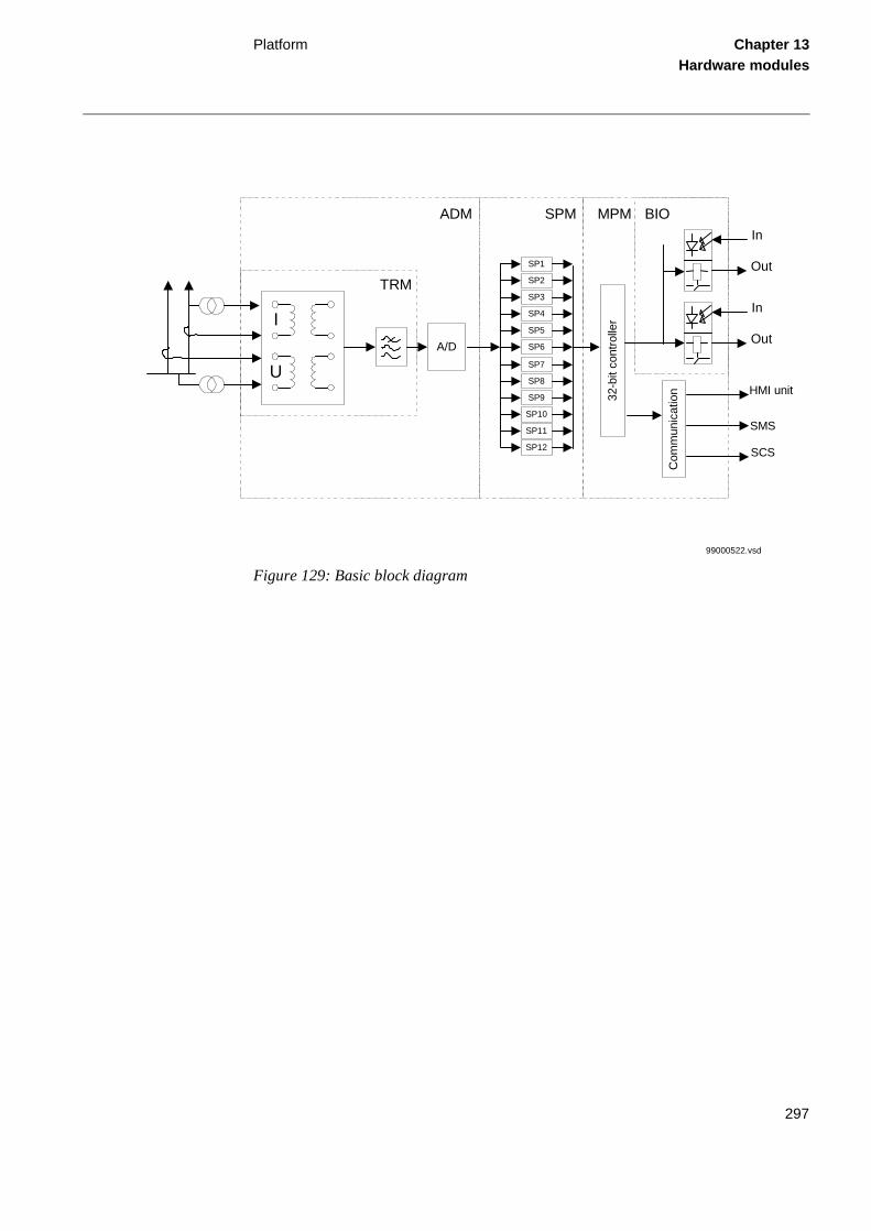
Platform Chapter 13Hardware modules
Figure 129: Basic block diagram
HMI unitU
IA/D
SP1
SP2
SP3
SP4
SP5
SP6
SP7
SP8
SP9
SP10
SP11
SP12
TRM
In
Out
In
Out
32-b
it co
ntro
ller
Com
mun
icat
ion
SCS
ADM SPM MPM BIO
SMS
99000522.vsd
297
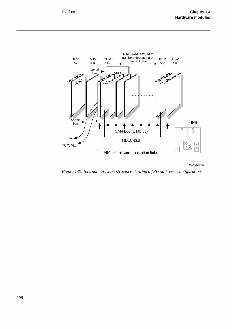
Platform Chapter 13Hardware modules
Figure 130: Internal hardware structure showing a full width case configuration
SA
PC/SMS
SPM
C
E
ShieldShield
Shield
TRMS2
ADMS8
MPMS10
BIM, BOM, IOM, MIMnumbers depending on
the rack sizeDCMS38
PSMS40
...............
CAN-bus (1 Mbit/s)
Analogbus
Serialbus
HDLC-bus
HMI
HMI serial communication links
99000526.vsd
298
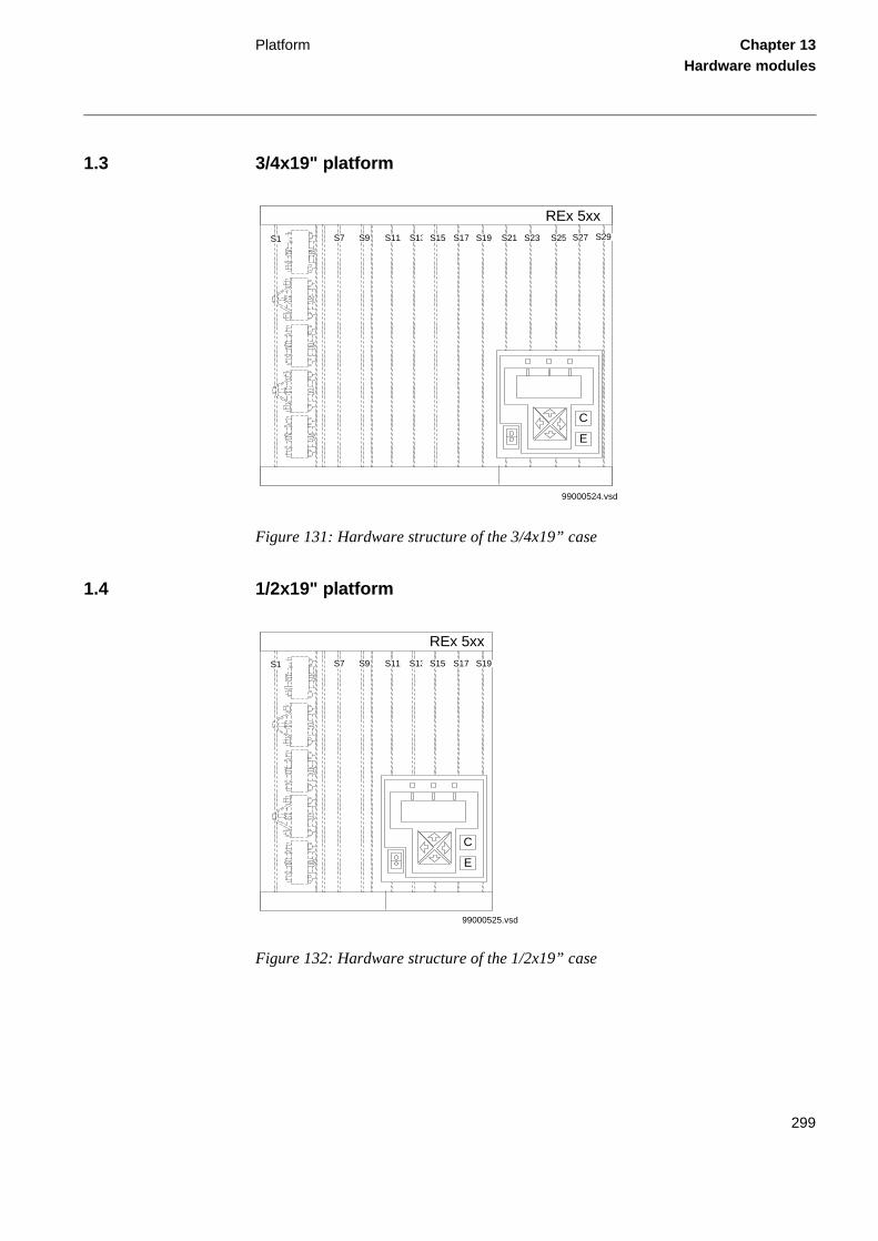
Platform Chapter 13Hardware modules
1.3 3/4x19" platform
Figure 131: Hardware structure of the 3/4x19” case
1.4 1/2x19" platform
Figure 132: Hardware structure of the 1/2x19” case
REx 5xxS1 S7 S9 S11 S13 S15 S17 S19 S21 S23 S25 S27 S29
C
E
99000524.vsd
REx 5xxS1 S7 S9 S11 S13 S15 S17 S19
C
E
99000525.vsd
299
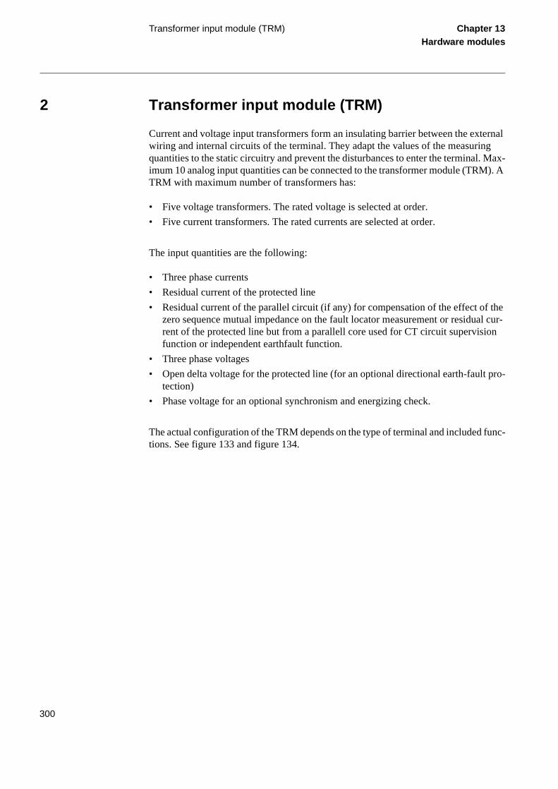
Transformer input module (TRM) Chapter 13Hardware modules
the l cur-n
pro-
func-
2 Transformer input module (TRM)
Current and voltage input transformers form an insulating barrier between the external wiring and internal circuits of the terminal. They adapt the values of the measuring quantities to the static circuitry and prevent the disturbances to enter the terminal. Max-imum 10 analog input quantities can be connected to the transformer module (TRM). A TRM with maximum number of transformers has:
• Five voltage transformers. The rated voltage is selected at order.
• Five current transformers. The rated currents are selected at order.
The input quantities are the following:
• Three phase currents
• Residual current of the protected line
• Residual current of the parallel circuit (if any) for compensation of the effect ofzero sequence mutual impedance on the fault locator measurement or residuarent of the protected line but from a parallell core used for CT circuit supervisiofunction or independent earthfault function.
• Three phase voltages
• Open delta voltage for the protected line (for an optional directional earth-faulttection)
• Phase voltage for an optional synchronism and energizing check.
The actual configuration of the TRM depends on the type of terminal and included tions. See figure 133 and figure 134.
300

Transformer input module (TRM) Chapter 13Hardware modules
Figure 133: Block diagram of the TRM for REL 551, Line differential protection
Bac
kpla
ne c
onne
ctor
Cur
rent
Inpu
t con
nect
or CT CT
CT
CT
CT
99000560.vsd
301
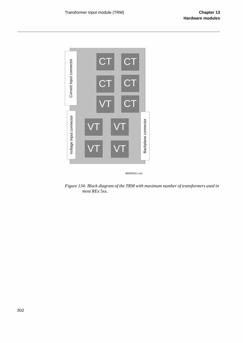
Transformer input module (TRM) Chapter 13Hardware modules
Figure 134: Block diagram of the TRM with maximum number of transformers used in most REx 5xx.
Bac
kpla
ne c
onne
ctor
Vol
tage
Inpu
t con
nect
orC
urre
nt In
put c
onne
ctor CT CT
CT
CT
CT
VT
VT
VT
VT
VT
990000511.vsd
302
A/D-conversion module (ADM) Chapter 13Hardware modules
3 A/D-conversion module (ADM)
The incoming signals from the intermediate current transformers are adapted to the electronic voltage level with shunts. To gain dynamic range for the current inputs, two shunts with separate A/D channels are used for each input current. By that a 16-bit dy-namic range is obtained with a 12 bits A/D converter.
The next step in the signal flow is the analogue filter of the first order, with a cut-off frequency of 500 Hz. This filter is used to avoid aliasing problems.
The A/D converter has a 12-bit resolution. It samples each input signal (5 voltages and 2x5 currents) with a sampling frequency of 2 kHz.
Before the A/D-converted signals are transmitted to the signal processing module, the signals are band-pass filtered and down-sampled to 1 kHz in a digital signal processor (DSP).
The filter in the DSP is a numerical filter with a cut-off frequency of 250 Hz.
The transmission of data between the A/D-conversion module and the signal processing module is done on a supervised serial link of RS485 type. This transmission is per-formed once every millisecond and contains information about all incoming analog sig-nals.
303

A/D-conversion module (ADM) Chapter 13Hardware modules
Figure 135: Block diagram for the ADM
Bac
kpla
ne c
onne
ctor
Analog filters ¤t shunts
PLD
DS
P
A/D
-co
nver
ter
Ana
log
MU
X
Controllogic &buffers
1-5 Voltageinputs
1-5 Currentinputs
99000512.vsd
304
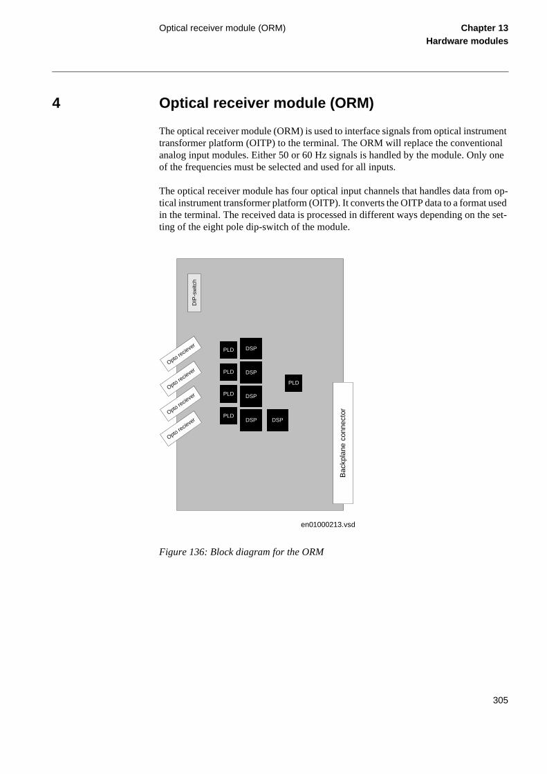
Optical receiver module (ORM) Chapter 13Hardware modules
4 Optical receiver module (ORM)
The optical receiver module (ORM) is used to interface signals from optical instrument transformer platform (OITP) to the terminal. The ORM will replace the conventional analog input modules. Either 50 or 60 Hz signals is handled by the module. Only one of the frequencies must be selected and used for all inputs.
The optical receiver module has four optical input channels that handles data from op-tical instrument transformer platform (OITP). It converts the OITP data to a format used in the terminal. The received data is processed in different ways depending on the set-ting of the eight pole dip-switch of the module.
Figure 136: Block diagram for the ORM
DIP
-sw
itch
Opto recie
verB
ackp
lane
con
nect
orPLD DSP
Opto recie
ver
Opto recie
ver
Opto recie
ver
PLD
PLD
PLD
DSP
DSP
DSP DSP
PLD
en01000213.vsd
305
Main processing module (MPM) Chapter 13Hardware modules
ine
5 Main processing module (MPM)
The terminal is based on a pipelined multi-processor design. The 32-bit main controller receives the result from the Signal processing module every millisecond.
All memory management are also handled by the main controller. The module has 8MB of disc memory and 1MB of code memory. It also has 8MB of dynamic memory.
The controller also serves four serial links: one high-speed CAN bus for Input/Output modules and three serial links for different types of HMI communication.
The main controller makes all decisions, based on the information from the Signal pro-cessing module and from the binary inputs. The decisions are sent to the different output modules and to these communication ports:
• Local HMI module including a front-connected PC, if any, for local human-machcommunication.
• LON communication port at the rear (option).
• SPA/IEC communication port at the rear (option)
306

Main processing module (MPM) Chapter 13Hardware modules
Figure 137: Block diagram for the MPM
To allow easy upgrading of software in the field a special connector is used, the Down-load connector.
Bac
kpla
ne c
onne
ctor
SP
M c
onne
ctor
Dow
nloa
dco
nnec
tor
Maincontroller
LON
CAN
DRAM (SIMM)
SP
A/IE
CLO
N
Disc Flash (8MB)
Code Flash (1MB)
8-bit Data bus
32-b
it D
ata
bus
CAN bus
SCM
SCM
99000513.vsd
307
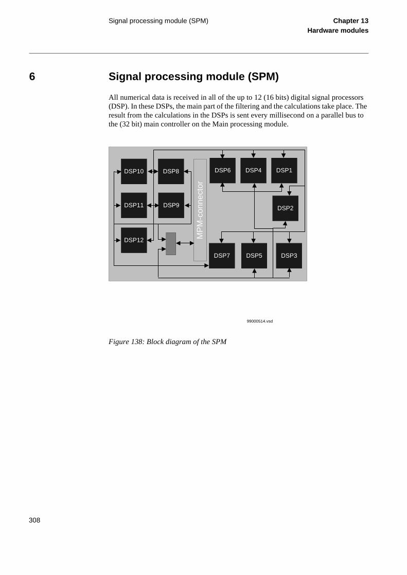
Signal processing module (SPM) Chapter 13Hardware modules
6 Signal processing module (SPM)
All numerical data is received in all of the up to 12 (16 bits) digital signal processors (DSP). In these DSPs, the main part of the filtering and the calculations take place. The result from the calculations in the DSPs is sent every millisecond on a parallel bus to the (32 bit) main controller on the Main processing module.
Figure 138: Block diagram of the SPM
DSP12
DSP11
DSP10 DSP8
DSP9
DSP6 DSP4 DSP1
DSP2
DSP3DSP5DSP7
MP
M-c
onne
ctor
99000514.vsd
308

Input/Output modules Chapter 13Hardware modules
7 Input/Output modules
7.1 General
The number of inputs and outputs in a REx 5xx terminal can be selected in a variety of combinations depending on the size of the rack. There is no basic I/O configuration of the terminal. The table below shows the number of available inputs or output modules for the different platform sizes.
A number of signals are available for signalling purposes in the terminal and all are freely programmable. The voltage level of the input/output modules is selectable at or-der. Available versions are RL 48, 110, or 220 (48/60 V +/-20%, 110/125 V +/-20% or 220/250 V +/-20%). The Binary in/out module and the Binary input module are also available in an RL 24 version (24/30 V +/-20%).
Figure 139 shows the operating characteristics of the binary inputs of the four voltage levels.
Platform size 1/1x19” 3/4x19” 1/2x19”
I/O slots available 13 8 3
309

Input/Output modules Chapter 13Hardware modules
Figure 139: Voltage dependence for the binary inputs
Table 17: Input voltage ranges explained
The I/O modules communicates with the Main Processing Module via the CAN-bus on the backplane.
The design of all binary inputs enables the burn off of the oxide of the relay contact con-nected to the input, despite the low, steady-state power consumption, which is shown in figure 140.
300
176
144
88
723832
19
18
24/30VRL24
48/60VRL48
110/125VRL110
220/250VRL220
[V]
xx99000517.vsd
Guaranteed operation
Operation uncertain
No operation
310
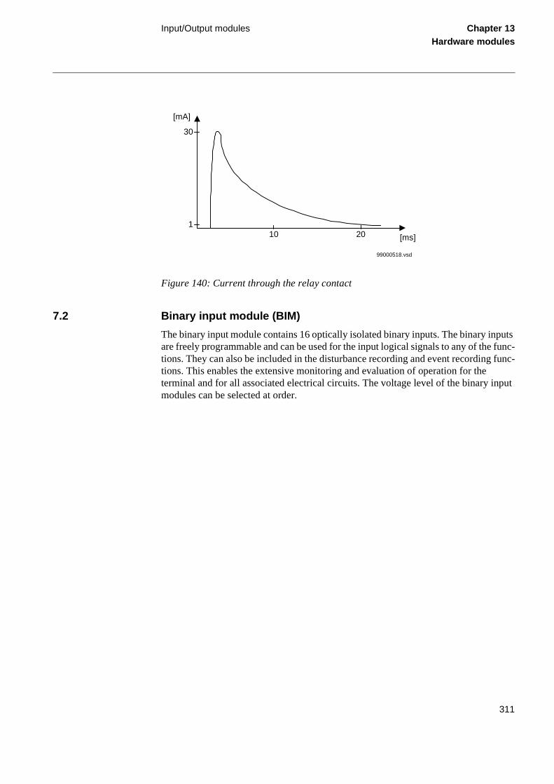
Input/Output modules Chapter 13Hardware modules
Figure 140: Current through the relay contact
7.2 Binary input module (BIM)
The binary input module contains 16 optically isolated binary inputs. The binary inputs are freely programmable and can be used for the input logical signals to any of the func-tions. They can also be included in the disturbance recording and event recording func-tions. This enables the extensive monitoring and evaluation of operation for the terminal and for all associated electrical circuits. The voltage level of the binary input modules can be selected at order.
30
110 20 [ms]
[mA]
99000518.vsd
311
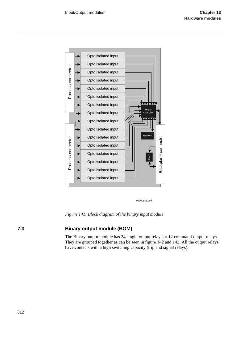
Input/Output modules Chapter 13Hardware modules
Figure 141: Block diagram of the binary input module
7.3 Binary output module (BOM)
The Binary output module has 24 single-output relays or 12 command-output relays. They are grouped together as can be seen in figure 142 and 143. All the output relays have contacts with a high switching capacity (trip and signal relays).
Bac
kpla
ne c
onne
ctor
Pro
cess
con
nect
orP
roce
ss c
onne
ctor
Micro-controller
Memory
CA
N
Opto isolated input
Opto isolated input
Opto isolated input
Opto isolated input
Opto isolated input
Opto isolated input
Opto isolated input
Opto isolated input
Opto isolated input
Opto isolated input
Opto isolated input
Opto isolated input
Opto isolated input
Opto isolated input
Opto isolated input
Opto isolated input
99000503.vsd
312
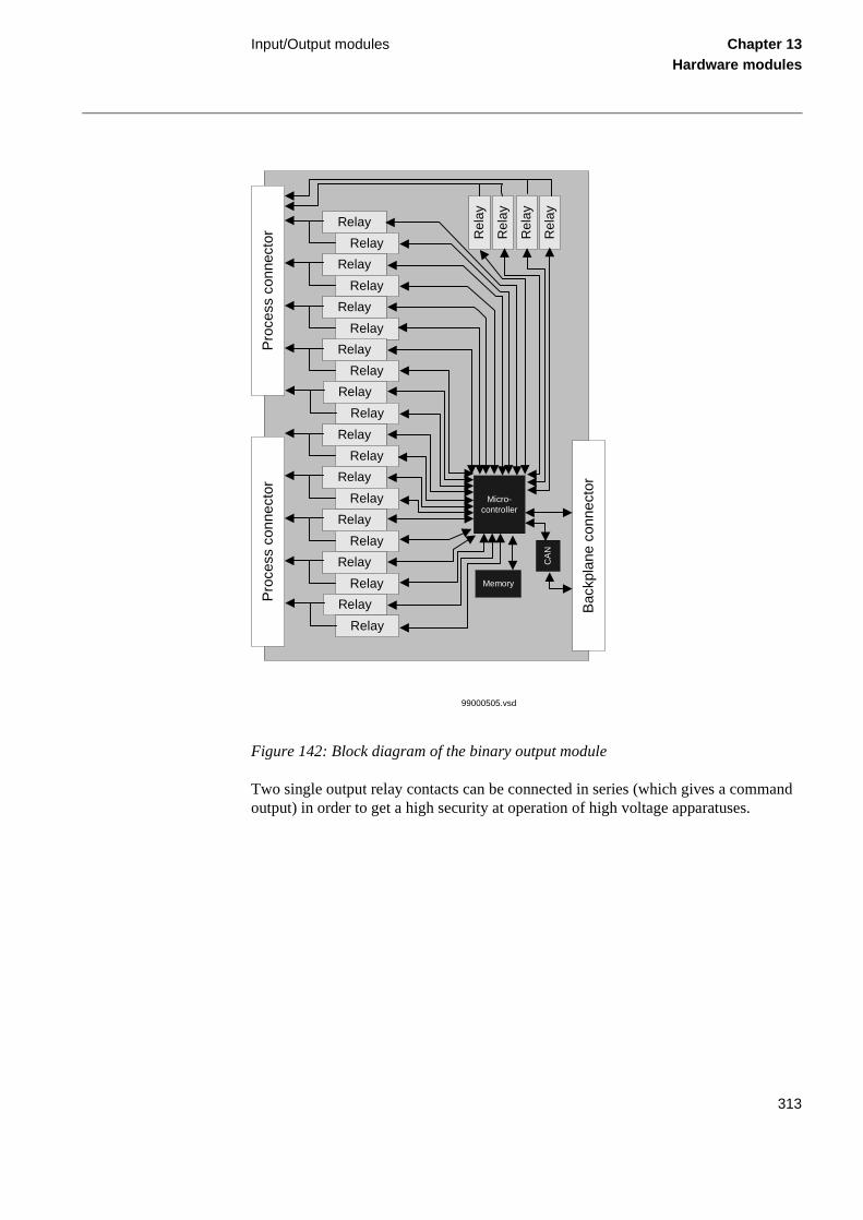
Input/Output modules Chapter 13Hardware modules
Figure 142: Block diagram of the binary output module
Two single output relay contacts can be connected in series (which gives a command output) in order to get a high security at operation of high voltage apparatuses.
Bac
kpla
ne c
onne
ctor
Pro
cess
con
nect
orP
roce
ss c
onne
ctor
Micro-controller
Memory
CA
N
Rel
ayRelay
Relay
Relay
Relay
Relay
Relay
Relay
Relay
Relay
Relay
Relay
Relay
Relay
Relay
Relay
Relay
Relay
Relay
Relay
Relay
Rel
ay
Rel
ay
Rel
ay
99000505.vsd
313
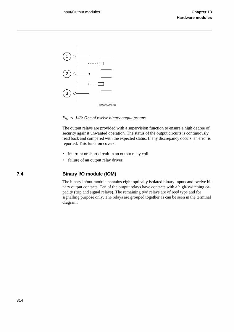
Input/Output modules Chapter 13Hardware modules
e bi-g ca-
rminal
Figure 143: One of twelve binary output groups
The output relays are provided with a supervision function to ensure a high degree of security against unwanted operation. The status of the output circuits is continuously read back and compared with the expected status. If any discrepancy occurs, an error is reported. This function covers:
• interrupt or short circuit in an output relay coil
• failure of an output relay driver.
7.4 Binary I/O module (IOM)
The binary in/out module contains eight optically isolated binary inputs and twelvnary output contacts. Ten of the output relays have contacts with a high-switchinpacity (trip and signal relays). The remaining two relays are of reed type and for signalling purpose only. The relays are grouped together as can be seen in the tediagram.
xx00000299.vsd
5
5
2
1
3
314

Input/Output modules Chapter 13Hardware modules
Figure 144: Block diagram for the binary input/output module
Bac
kpla
ne c
onne
ctor
Pro
cess
con
nect
orP
roce
ss c
onne
ctor
Relay
Relay
Relay
Relay
Relay
Relay
Relay
Relay
Relay
Relay
Rel
ay
Rel
ay
Relay Relay
Micro-controller
PWM
Memory
CA
N
Deb
ug&
isp
Opto isolated input
Opto isolated input
Opto isolated input
Opto isolated input
Opto isolated input
Opto isolated input
Opto isolated input
Opto isolated input
99000502vsd
315
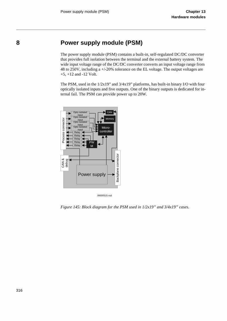
Power supply module (PSM) Chapter 13Hardware modules
ur r in-
8 Power supply module (PSM)
The power supply module (PSM) contains a built-in, self-regulated DC/DC converter that provides full isolation between the terminal and the external battery system. The wide input voltage range of the DC/DC converter converts an input voltage range from 48 to 250V, including a +/-20% tolerance on the EL voltage. The output voltages are +5, +12 and -12 Volt.
The PSM, used in the 1/2x19” and 3/4x19” platforms, has built-in binary I/O with fooptically isolated inputs and five outputs. One of the binary outputs is dedicated foternal fail. The PSM can provide power up to 20W.
Figure 145: Block diagram for the PSM used in 1/2x19” and 3/4x19” cases.
Bac
kpla
ne c
onne
ctor
Pro
cess
con
nect
orC
AN
&de
bug
Opto isolatedinput
Opto isolatedinput
Opto isolatedinput
Opto isolatedinput
RelayRelayRelayRelayRelay
Power supply
Micro-controller
Memory
PWM
CAN
99000515.vsd
316
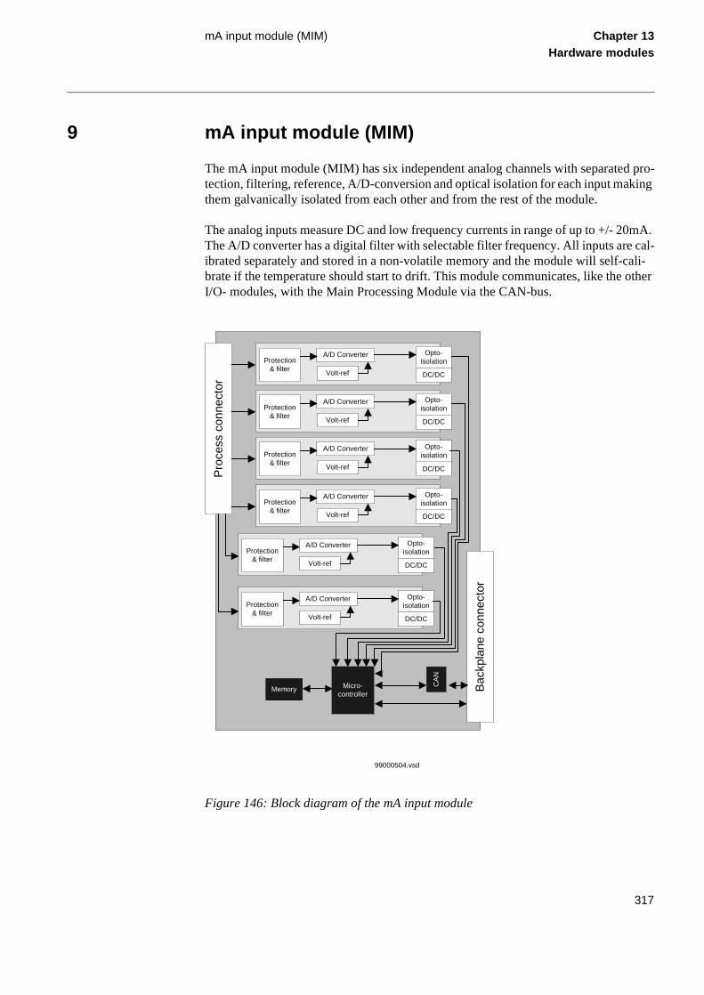
mA input module (MIM) Chapter 13Hardware modules
9 mA input module (MIM)
The mA input module (MIM) has six independent analog channels with separated pro-tection, filtering, reference, A/D-conversion and optical isolation for each input making them galvanically isolated from each other and from the rest of the module.
The analog inputs measure DC and low frequency currents in range of up to +/- 20mA. The A/D converter has a digital filter with selectable filter frequency. All inputs are cal-ibrated separately and stored in a non-volatile memory and the module will self-cali-brate if the temperature should start to drift. This module communicates, like the other I/O- modules, with the Main Processing Module via the CAN-bus.
Figure 146: Block diagram of the mA input module
Bac
kpla
ne c
onne
ctor
Pro
cess
con
nect
or
Micro-controller
Memory
CA
N
Protection& filter
A/D Converter
Volt-ref
Opto-isolation
DC/DC
Protection& filter
A/D Converter
Volt-ref
Opto-isolation
DC/DC
Protection& filter
A/D Converter
Volt-ref
Opto-isolation
DC/DC
Protection& filter
A/D Converter
Volt-ref
Opto-isolation
DC/DC
Protection& filter
A/D Converter
Volt-ref
Opto-isolation
DC/DC
Protection& filter
A/D Converter
Volt-ref
Opto-isolation
DC/DC
99000504.vsd
317
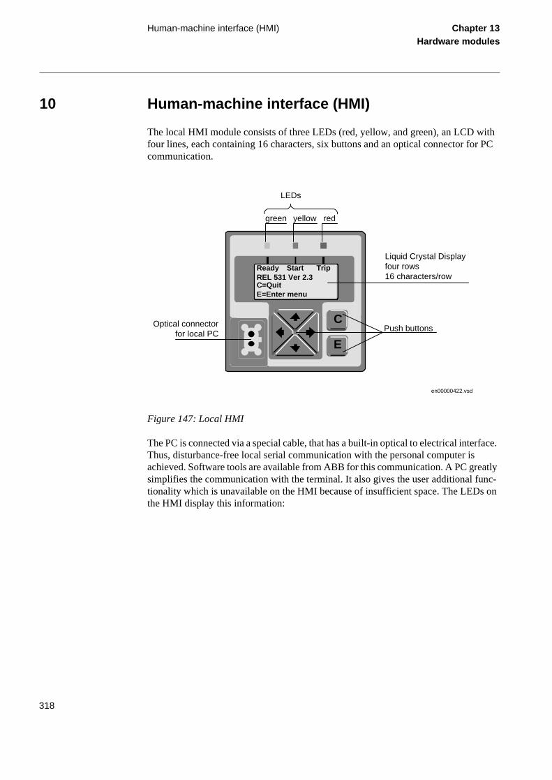
Human-machine interface (HMI) Chapter 13Hardware modules
10 Human-machine interface (HMI)
The local HMI module consists of three LEDs (red, yellow, and green), an LCD with four lines, each containing 16 characters, six buttons and an optical connector for PC communication.
Figure 147: Local HMI
The PC is connected via a special cable, that has a built-in optical to electrical interface. Thus, disturbance-free local serial communication with the personal computer is achieved. Software tools are available from ABB for this communication. A PC greatly simplifies the communication with the terminal. It also gives the user additional func-tionality which is unavailable on the HMI because of insufficient space. The LEDs on the HMI display this information:
en00000422.vsd
E
C
ReadyREL 531 Ver 2.3C=QuitE=Enter menu
Start Trip
Push buttons
green yellow red
LEDs
Liquid Crystal Displayfour rows16 characters/row
Optical connectorfor local PC
318
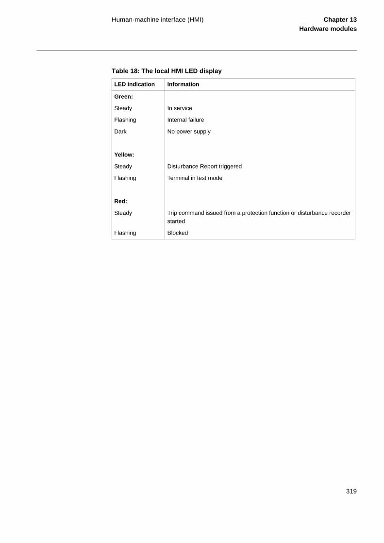
Human-machine interface (HMI) Chapter 13Hardware modules
Table 18: The local HMI LED display
LED indication Information
Green:
Steady
Flashing
Dark
Yellow:
Steady
Flashing
Red:
Steady
Flashing
In service
Internal failure
No power supply
Disturbance Report triggered
Terminal in test mode
Trip command issued from a protection function or disturbance recorder started
Blocked
319

Human-machine interface (HMI) Chapter 13Hardware modules
320