Embed Size (px)
Citation preview
BGA (Ball Grid Array)
CONTENTS
Introduction
Package Overview
PBGA Construction
EBGA Construction
Package Handling/Shipping Media
Design Recommendations
Solder Pad Geometry
Escape Routing Guidlines
Via Density
Assembly Recommendations
Process Flow and Set-up Recommendations
PCB Plating Recommendations
Solder Paste Printing
Paste Recommendations
Component Placement
Reflow and Cleaning
Solder Joint Inspection
Replacement / Rework
Removal of the BGA
Site Preparation
Solder Paste Deposition
Component Placement
Component Reflow
Appendices
Solder Joint Reliability
INTRODUCTION
The consumer electronics industry is constantly seeking so-lutions that will resolve challenges to design their solutionssmaller and less expensive. The Ball Grid Array (BGA) Pack-age has impacted one of the industry’s most limiting designfactors, board real estate and its increasing cost. The costcan be indirectly related to the lost revenue caused by acompetitive disadvantage when the competition’s solution issmaller, better, and contains more functionality. Today’ssemiconductor, packaging and printed circuit board (PCB)manufacturing technologies make it possible to fit camcord-ers in the palm of your hand and cell phones and PDA’s inyour shirt pocket. These applications require PCB densitiesthat include components on the top and bottom sides of theboard. The BGA package is one solution that addresses thisconcern.
The many benefits of using BGA over similar lead countleaded devices include:
1. Efficient use of board space.
2. Improved thermal and electrical performance and easeof enhancing both.
3. Compatibility with existing surface mount, test and han-dling equipment.
4. Improved surface mount yields when compared to finepitch leaded devices.
5. Lower profile (package thickness).
6. Potential lower total cost of ownership compared toleaded devices due to reduced scrap, rework and lack ofneed for fine pitch assembly equipment.
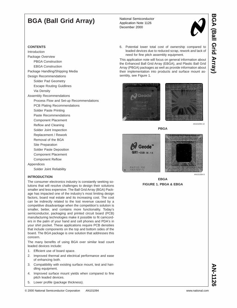
This application note will focus on general information aboutthe Enhanced Ball Grid Array (EBGA), and Plastic Ball GridArray (PBGA) packages as well as provide information abouttheir implementation into products and surface mount as-sembly, see Figure 1.
AN101094-10
PBGA
AN101094-9
EBGA
FIGURE 1. PBGA & EBGA
National SemiconductorApplication Note 1126December 2000
BG
A(B
allGrid
Array)
AN
-1126
© 2000 National Semiconductor Corporation AN101094 www.national.com
PACKAGE OVERVIEW
PBGA Construction
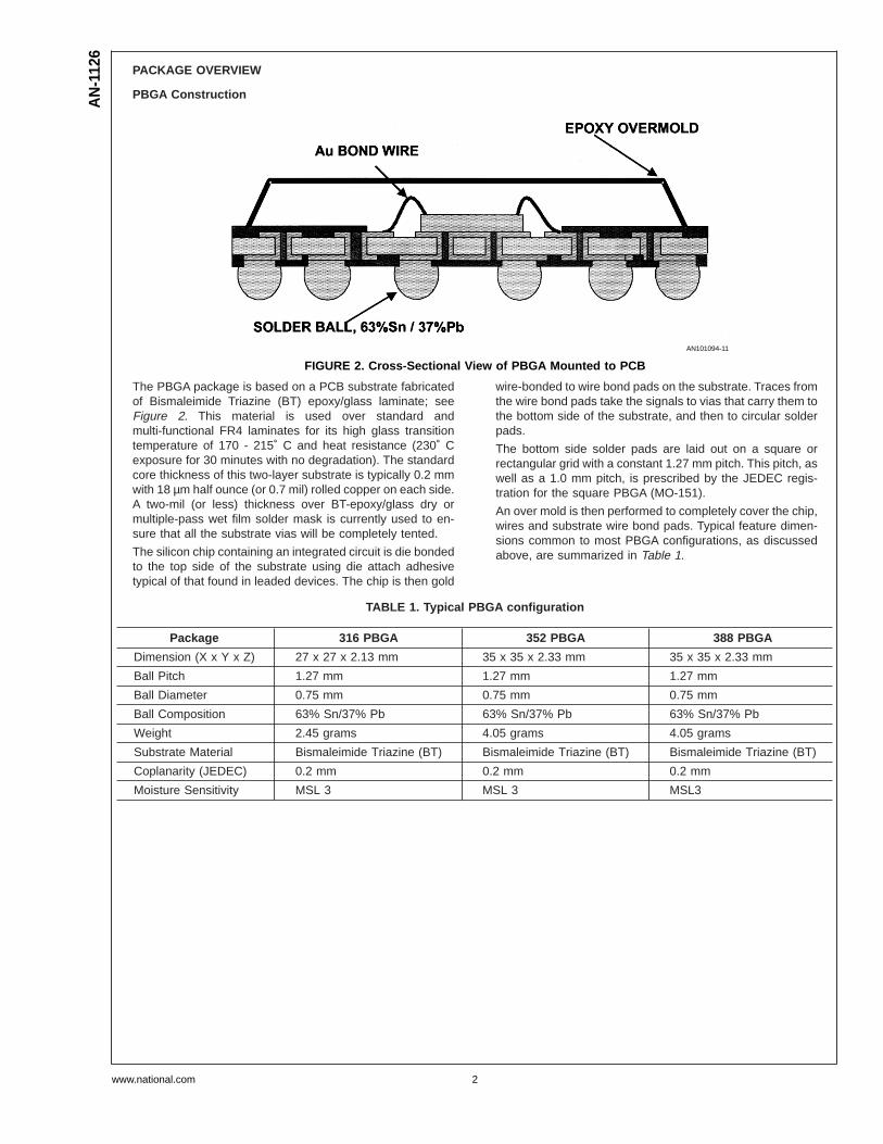
The PBGA package is based on a PCB substrate fabricatedof Bismaleimide Triazine (BT) epoxy/glass laminate; seeFigure 2. This material is used over standard andmulti-functional FR4 laminates for its high glass transitiontemperature of 170 - 215˚ C and heat resistance (230˚ Cexposure for 30 minutes with no degradation). The standardcore thickness of this two-layer substrate is typically 0.2 mmwith 18 µm half ounce (or 0.7 mil) rolled copper on each side.A two-mil (or less) thickness over BT-epoxy/glass dry ormultiple-pass wet film solder mask is currently used to en-sure that all the substrate vias will be completely tented.
The silicon chip containing an integrated circuit is die bondedto the top side of the substrate using die attach adhesivetypical of that found in leaded devices. The chip is then gold
wire-bonded to wire bond pads on the substrate. Traces fromthe wire bond pads take the signals to vias that carry them tothe bottom side of the substrate, and then to circular solderpads.
The bottom side solder pads are laid out on a square orrectangular grid with a constant 1.27 mm pitch. This pitch, aswell as a 1.0 mm pitch, is prescribed by the JEDEC regis-tration for the square PBGA (MO-151).
An over mold is then performed to completely cover the chip,wires and substrate wire bond pads. Typical feature dimen-sions common to most PBGA configurations, as discussedabove, are summarized in Table 1.
TABLE 1. Typical PBGA configuration
Package 316 PBGA 352 PBGA 388 PBGA
Dimension (X x Y x Z) 27 x 27 x 2.13 mm 35 x 35 x 2.33 mm 35 x 35 x 2.33 mm
Ball Pitch 1.27 mm 1.27 mm 1.27 mm
Ball Diameter 0.75 mm 0.75 mm 0.75 mm
Ball Composition 63% Sn/37% Pb 63% Sn/37% Pb 63% Sn/37% Pb
Weight 2.45 grams 4.05 grams 4.05 grams
Substrate Material Bismaleimide Triazine (BT) Bismaleimide Triazine (BT) Bismaleimide Triazine (BT)
Coplanarity (JEDEC) 0.2 mm 0.2 mm 0.2 mm
Moisture Sensitivity MSL 3 MSL 3 MSL3
AN101094-11
FIGURE 2. Cross-Sectional View of PBGA Mounted to PCB
AN
-112
6
www.national.com 2
EBGA Construction
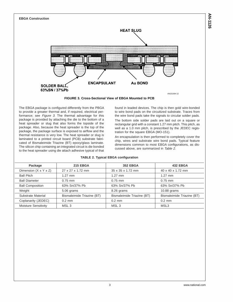
The EBGA package is configured differently from the PBGAto provide a greater thermal and, if required, electrical per-formance; see Figure 3. The thermal advantage for thispackage is provided by attaching the die to the bottom of aheat spreader or slug that also forms the topside of thepackage. Also, because the heat spreader is the top of thepackage, the package surface is exposed to airflow and thethermal resistance is very low. The heat spreader or slug islaminated to a printed circuit board (PCB) substrate fabri-cated of Bismaleimide Triazine (BT) epoxy/glass laminate.The silicon chip containing an integrated circuit is die bondedto the heat spreader using die attach adhesive typical of that
found in leaded devices. The chip is then gold wire-bondedto wire bond pads on the circuitized substrate. Traces fromthe wire bond pads take the signals to circular solder pads.
The bottom side solder pads are laid out on a square orrectangular grid with a constant 1.27 mm pitch. This pitch, aswell as a 1.0 mm pitch, is prescribed by the JEDEC regis-tration for the square EBGA (MO-151).
An encapsulation is then performed to completely cover thechip, wires and substrate wire bond pads. Typical featuredimensions common to most EBGA configurations, as dis-cussed above, are summarized in Table 2.
TABLE 2. Typical EBGA configuration
Package 215 EBGA 352 EBGA 432 EBGA
Dimension (X x Y x Z) 27 x 27 x 1.72 mm 35 x 35 x 1.72 mm 40 x 40 x 1.72 mm
Ball Pitch 1.27 mm 1.27 mm 1.27 mm
Ball Diameter 0.75 mm 0.75 mm 0.75 mm
Ball Composition 63% Sn/37% Pb 63% Sn/37% Pb 63% Sn/37% Pb
Weight 5.06 grams 8.26 grams 10.88 grams
Substrate Material Bismaleimide Triazine (BT) Bismaleimide Triazine (BT) Bismaleimide Triazine (BT)
Coplanarity (JEDEC) 0.2 mm 0.2 mm 0.2 mm
Moisture Sensitivity MSL 3 MSL 3 MSL3
AN101094-12
FIGURE 3. Cross-Sectional View of EBGA Mounted to PCB
AN
-1126
www.national.com3

PACKAGE HANDLING/SHIPPING MEDIA
The BGA packages are shipped in a high temperaturerange thin matrix tray that complies with the JEDEC stan-dards. Typical JEDEC trays have the same ’x’ and ’y’outer dimensions and are easily stacked for storage andmanufacturing.
DESIGN RECOMMENDATIONS
Solder Pad Geometry
Two types of land patterns are used for surface mountpackages: 1) Non-Solder Mask Defined pads (NSMD)and, 2) Solder Mask Defined pads (SMD). NSMD has anopening that is larger than the pad, whereas SMD padshave a solder mask opening that is smaller than the metalpad. Figure 4 illustrates the two different types of padgeometry.
NSMD is preferred because the copper etch process hastighter control than the solder masking process.
NSMD pads require a ±0.075 mm clearance around thecopper pad and solder mask this avoids overlap betweenthe solder joint and solder mask and accounts for maskregistration tolerances.
SMD pad definition can introduce stress concentrationpoints near the solder mask on the PCB side. Extremeenvironmental conditions such as large temperaturevariations may cause fatigue that leads to cracked solderjoints and reliability problems.
For optimal reliability, National recommends a 1:1 ratiobetween the package pad and the PCB pad for the BGAwherever trace routing is not a constraint. The ratio maybe reduced to 1:0.8 if absolutely necessary. See Table 3.
TABLE 3. Guidelines for Pad Design
PBGA 352 ball with 1.27 mmpitch
NSMD SMD
Solder Ball Diameter 0.75 mm 0.75 mm
PCB Pad Diameter 0.64 mm 0.78 mm
Solder Mask OpeningDiameter
0.78 mm 0.64 mm
Escape Routing Guidelines
A typical PBGA substrate has four or five rows of solder ballsaround the periphery of the package, which provides inter-connection to the PCB. The number of lines routed (N)between the pads on the PCB is defined by the pad size andthe line width and spacing capabilities of the PCB manufac-turer. The following relation ship is used to define N:
For NSMD pads, exposure of underlying copper traces isforbidden, so the diameter and tolerance of the solder maskopening define D.
The number of routing lines as a function of pad pitch forvarious PCB line space/width geometries is shown in Table4. Routing assumes a four-layer board (2 signal and 2ground) with NSMD pads on the PCB. The package pad toPCB pad ratio is 1:1.
TABLE 4. Recommended Number of Routing Line
Pad pitch 1.27 mm
L/S = 0.15 mm 1
L/S = 0.125 mm 2
L/S = 0.10 mm 2
Either a 1.0 or 1.27 mm pitch PBGA with four rows of solderballs can be routed to a four layer PCB (Figure 5) using a0.15 mm (6 mil) line/space. The first two ball rows can berouted to one signal layer while the third and fourth ball rowscan be routed to a second signal layer.
Routing possibilities become more complicated for afour-layer board, if there are five rows of solder balls. For a1.27 mm ball pitch PBGA, a 0.125 mm (5 mil) PCB line/space design will be necessary for routing (Figure 6). A 1.0mm PBGA will require a 0.10 mm (4 mil) line/space tosuccessfully route 5 rows of solder balls to a four-layer PCB(Figure 7). For both packages, the first three ball rows arerouted to one signal layer while the fourth and fifth ball rowsare routed to a second signal layer.
AN101094-1
FIGURE 4. NSMD and SMD Pad Definition
AN101094-2
P = Pad PitchD = Pad Diameter
L = Line WidthS = Line Space
AN101094-3
FIGURE 5. Routing for Four Rows of Solder Balls
AN
-112
6
www.national.com 4

Via Density
Via density has a significant impact on the routability ofPBGA, especially as the solder ball pitch decreases to 0.8mm. Figure 8 shows the routability of a 0.8 mm ball pitchPBGA using 0.1 mm line space and width. Mechanicallydrilled holes below 0.30 mm (12 mil) in diameter, begin toadd substantial cost to the PCB, with 0.20 mm (8 mil) beingthe minimum diameter that can be typically drilled in high-volume PCB manufacturing. As traditional PCB material andprocesses have been pushed to the limit and are unsatisfac-tory in meeting the wiring densities, new PCB manufacturingtechnologies have emerged. Table 5 list trends for PCB usedin portable computers.
AN101094-4
FIGURE 6. Routing for Five Rows of Solder Balls
AN101094-5
FIGURE 7. Routing for Five Rows of Solder Balls
AN
-1126
www.national.com5

TABLE 5. Feature Trends for Portable Computer PCB’s
1997 2000 2002
Number of Layers 5 - 8 7 - 9 7 - 10
Inner Layer Thickness (mm) 0.1 0.7 0.5
Via Diameter (mm) 0.28 0.125 0.1
Land Diameter (mm) 0.48 0.25 0.25
Line Space/Width (mm) 0.1 0.075 0.05
To increase wiring density and improve electrical perfor-mance, thin layers are fabricated onto a PCB core with smallmicro-vias. These micro-via technologies are referred to asbuild-up-board (BUB) technologies and are cost-effectivealternatives to PCB processes for manufacturing board sub-strates.
There are many variations of BUB boards, though a genericstructure consists of two-layers of un-reinforced epoxy di-electric coated on to a rigid (core). Micro-vias are typicallyformed using either laser or photolithography processes.The fabrication of BUB boards requires new processes andmaterials compared to standard PCB technologies. Table 6shows some micro-via geometries available to facilitate therouting of BGA packages.
The cost trade-offs for deciding on a micro-via PCB designcompared to a standard PCB design is a function of the viaforming process, materials used, and the number of vias.Consult your PCB manufacturer for a detailed cost analysis.
TABLE 6. Available Micro-Via Geometries
Line Width (mm) 0.07 - 0.1
Line Space (mm) 0.075 - 0.1
Micro-via Hole Size (mm) 0.075 - 0.1
Micro-via Pad (mm) 0.2 - 0.3
Drilled Through Hole (core)(µm)
250
Drilled Through Hole Pad(µm)
500
Buried Via Hole (µm) 200
Buried Via Capture Pad (µm) 450
AN101094-7
FIGURE 8. Routing for Three Rows of Solder Balls
AN
-112
6
www.national.com 6
ASSEMBLY RECOMMENDATIONS
Process Flow & Set-up Recommendation:
The BGA surface mount assembly operations include:
• PCB plating requirements
• Screen printing the solder paste on the PCB
• Monitoring the solder paste volume (uniformity)
• Package placement using standard SMT placementequipment
• X-ray pre reflow check - paste bridging
• Reflow and cleaning (dependent upon the flux type)
• X-ray post reflow check - solder bridging & voids
PCB Plating Recommendations:
A uniform PCB plating thickness is key for high assemblyyield.
• PCB with Organic Solderability Preservative coating(OSP) finish is recommended.
• For PCBs with electroless, nickel-immersion, gold finish,the gold thickness recommendation is 0.15 µm ± 0.05 µmto avoid solder joint embrittlement and ensure solderabil-ity to the nickel.
Solder Paste Printing
Solder paste deposition using a stencil-printing process in-volves the transfer of the solder paste through pre-definedapertures with the application of pressure. Stencil param-eters such as aperture area ratio and the fabrication processhave a significant impact on paste deposition. Inspection ofthe stencil prior to placement of the BGA package is highlyrecommended to improve board assembly yields.Three typical stencil fabrication methods include:
• Chem-etch
• Laser cut
• Metal additive processes
Nickel-plated electro polished chem-etch or Laser cutwith tapered aperture walls (5˚ tapering) is recommendedto facilitate paste release. The recommended aperturesize is 0.1 mm larger than the pad size to allow 0.05 mmoverprinting on each side.
Paste Recommendations
No clean type 3 or 4 paste is recommended.
Component Placement
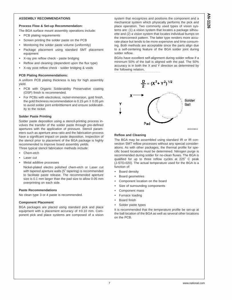
BGA packages are placed using standard pick and placeequipment with a placement accuracy of ±0.10 mm. Com-ponent pick and place systems are composed of a vision
system that recognizes and positions the component and amechanical system which physically performs the pick andplace operation. Two commonly used types of vision sys-tems are: (1) a vision system that locates a package silhou-ette and (2) a vision system that locates individual bumps onthe interconnect pattern. The latter type renders more accu-rate place but tends to be more expensive and time consum-ing. Both methods are acceptable since the parts align dueto a self-centering feature of the BGA solder joint duringsolder reflow.
BGAs have excellent self-alignment during solder reflow if aminimum 50% of the ball is aligned with the pad. The 50%accuracy is in both the X and Y direction as determined bythe following relation,50% misalignment for a 0.63 mm and 0.35 mm diameter pads are ±0.22 mm and ±0.12 mm, respectively. As stated above, standard pick and place equipment can accurately place components within this degree of accuracy.
Reflow and Cleaning
The BGA may be assembled using standard IR or IR con-vection SMT reflow processes without any special consider-ations. As with other packages, the thermal profile for spe-cific board locations must be determined. Nitrogen purge isrecommended during solder for no-clean fluxes. The BGA isqualified for up to three reflow cycles at 225˚ C peak(J-STD-020). The actual temperature used for the BGA is afunction of:
• Board density
• Board geometries
• Component location on the board
• Size of surrounding components
• Component mass
• Furnace loading
• Board finish
• Solder paste types
It is recommended that the temperature profile be set-up atthe ball location of the BGA as well as several other locationson the PCB.
AN101094-8
AN
-1126
www.national.com7
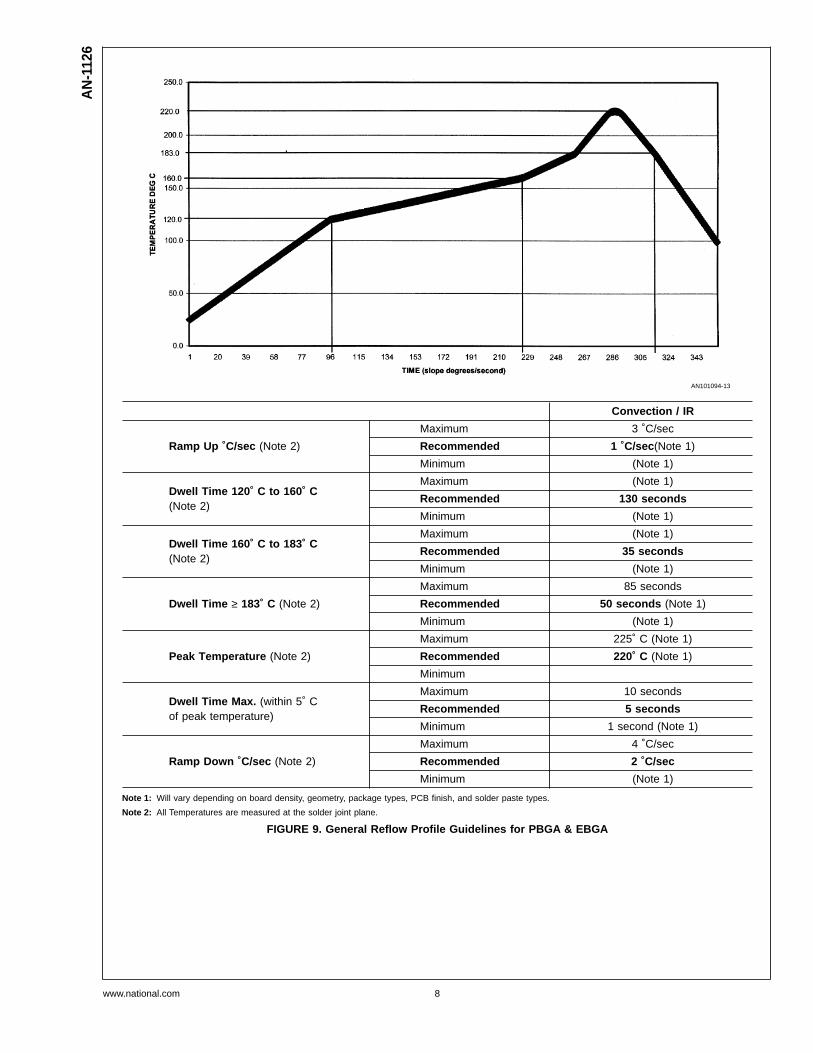
AN101094-13
Convection / IR
Ramp Up ˚C/sec (Note 2)
Maximum 3 ˚C/sec
Recommended 1 ˚C/sec (Note 1)
Minimum (Note 1)
Dwell Time 120˚ C to 160˚ C(Note 2)
Maximum (Note 1)
Recommended 130 seconds
Minimum (Note 1)
Dwell Time 160˚ C to 183˚ C(Note 2)
Maximum (Note 1)
Recommended 35 seconds
Minimum (Note 1)
Dwell Time ≥ 183˚ C (Note 2)
Maximum 85 seconds
Recommended 50 seconds (Note 1)
Minimum (Note 1)
Peak Temperature (Note 2)
Maximum 225˚ C (Note 1)
Recommended 220˚ C (Note 1)
Minimum
Dwell Time Max. (within 5˚ Cof peak temperature)
Maximum 10 seconds
Recommended 5 seconds
Minimum 1 second (Note 1)
Ramp Down ˚C/sec (Note 2)
Maximum 4 ˚C/sec
Recommended 2 ˚C/sec
Minimum (Note 1)
Note 1: Will vary depending on board density, geometry, package types, PCB finish, and solder paste types.
Note 2: All Temperatures are measured at the solder joint plane.
FIGURE 9. General Reflow Profile Guidelines for PBGA & EBGA
AN
-112
6
www.national.com 8
Solder Joint Inspection
After surface mount assembly, transmission X-ray should beused for sample monitoring of the solder attachment pro-cess. This identifies defects such as solder bridging, shorts,opens and voids. Note: Voids, up to 25% of the solder jointarea, typically do not have an impact on solder joint reliabil-ity.
Replacement/ Rework
The quality of the rework is controlled by directing the ther-mal energy through the component body to solder withoutover-heating the adjacent components.
Heating should occur in an encapsulated, inert, gas-purgedenvironment where the temperature gradients do not exceed±5˚ C across the heating zone using a convective bottomside pre-heater to maximize temperature uniformity. Inter-changeable nozzles designed with different geometries willaccommodate different applications to direct the airflow pathNOTE: Industry standard SMT rework systems include theseelements.
Removal of the BGA
Removing the BGA from the PCB involves heating the solderjoints above the liquidus temperature of eutectic(63Sn-37Pb) solder using a vacuum gas nozzle. Baking thePCB at 125˚ C for 4 hours is recommended PRIOR to anyrework. Doing this removes any residual moisture from thesystem, preventing moisture induced cracking or PCBdelamination during the demount process.
A 1.27 mm (50 mil) keep-out zone for adjacent componentsis recommended for standard rework processing. If the ad-jacent components are closer than 1.27 mm, custom toolsare required for the removal and rework of the package.
It is recommended that the reflow profile used to reflow theBGA be as close to the PCB mount profile as possible.Preheat the PCB area, through the bottom side of the board,to 100˚ C before heating the BGA to ensure a controlledprocess. Once the liquidus temperature is reached, nozzlevacuum is automatically activated and the component isremoved. After removing the package, the pads may beheated with the nozzle to reflow any residual solder, whichmay be removed using Teflon tipped vacuum wand.
Site Preparation
Once the BGA is removed, the site must be cleaned inpreparation for package attachment. The best results areachieved with a low-temperature, blade-style conductive toolmatching the footprint area of the BGA in conjunction with ade-soldering braid. No-clean flux is needed throughout theentire rework process. Care must be taken to avoid burn,lift-off, or damage of the PCB attachment area.
Solder Paste Deposition
Because the BGA is a land area type package, solder pasteis required to insure proper solder joint formation after re-work. A 100 µm thick mini-stencil is recommended to depositthe solder paste patterns prior to replacement of the BGA.
Component Placement
Most BGA rework stations will have a pick and place featurefor accurate placement and alignment. Manual pick andplace, with only eyeball alignment, is not recommended. It isdifficult to achieve consistent placement accuracy.
Component Reflow
It is recommended that the reflow profile used to reflow theBGA be as close to the PCB mount profile as possible.Preheat the PCB area, through the bottom side of the board,to 100˚ C before heating the BGA to ensure a controlledprocess. Once the liquidus temperature is reached, the sol-der will reflow and the BGA will self align. NOTE: Insure thereplacement BGA meets the Moisture Sensitivity Level re-quirements to prevent moisture-induced problems.
AN
-1126
www.national.com9
APPENDICES
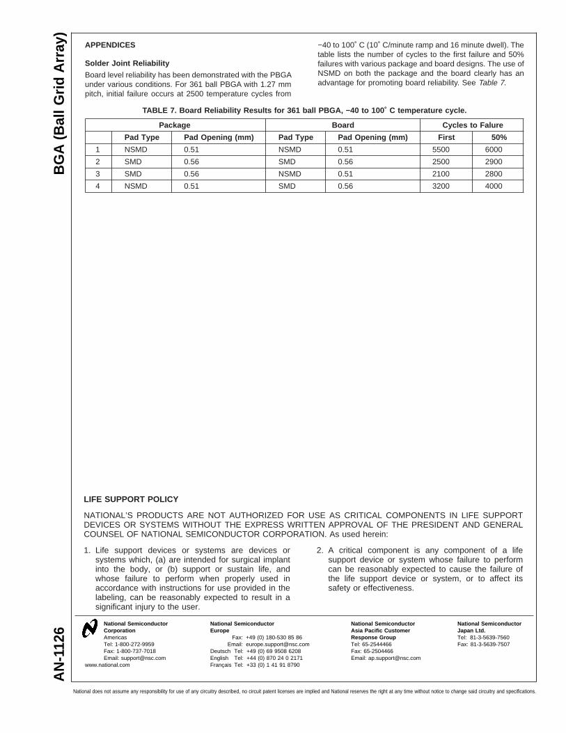
Solder Joint Reliability
Board level reliability has been demonstrated with the PBGAunder various conditions. For 361 ball PBGA with 1.27 mmpitch, initial failure occurs at 2500 temperature cycles from
−40 to 100˚ C (10˚ C/minute ramp and 16 minute dwell). Thetable lists the number of cycles to the first failure and 50%failures with various package and board designs. The use ofNSMD on both the package and the board clearly has anadvantage for promoting board reliability. See Table 7.
TABLE 7. Board Reliability Results for 361 ball PBGA, −40 to 100˚ C temperature cycle.
Package Board Cycles to Falure
Pad Type Pad Opening (mm) Pad Type Pad Opening (mm) First 50%
1 NSMD 0.51 NSMD 0.51 5500 6000
2 SMD 0.56 SMD 0.56 2500 2900
3 SMD 0.56 NSMD 0.51 2100 2800
4 NSMD 0.51 SMD 0.56 3200 4000
LIFE SUPPORT POLICY
NATIONAL’S PRODUCTS ARE NOT AUTHORIZED FOR USE AS CRITICAL COMPONENTS IN LIFE SUPPORTDEVICES OR SYSTEMS WITHOUT THE EXPRESS WRITTEN APPROVAL OF THE PRESIDENT AND GENERALCOUNSEL OF NATIONAL SEMICONDUCTOR CORPORATION. As used herein:
1. Life support devices or systems are devices orsystems which, (a) are intended for surgical implantinto the body, or (b) support or sustain life, andwhose failure to perform when properly used inaccordance with instructions for use provided in thelabeling, can be reasonably expected to result in asignificant injury to the user.
2. A critical component is any component of a lifesupport device or system whose failure to performcan be reasonably expected to cause the failure ofthe life support device or system, or to affect itssafety or effectiveness.
National SemiconductorCorporationAmericasTel: 1-800-272-9959Fax: 1-800-737-7018Email: [email protected]
National SemiconductorEurope
Fax: +49 (0) 180-530 85 86Email: [email protected]
Deutsch Tel: +49 (0) 69 9508 6208English Tel: +44 (0) 870 24 0 2171Français Tel: +33 (0) 1 41 91 8790
National SemiconductorAsia Pacific CustomerResponse GroupTel: 65-2544466Fax: 65-2504466Email: [email protected]
National SemiconductorJapan Ltd.Tel: 81-3-5639-7560Fax: 81-3-5639-7507
www.national.com
AN
-112
6B
GA
(Bal
lGrid
Arr
ay)
National does not assume any responsibility for use of any circuitry described, no circuit patent licenses are implied and National reserves the right at any time without notice to change said circuitry and specifications.