Embed Size (px)
Citation preview
IR HiRel web link: click here December 20, 2017
1
AN-1222
Application Note AN-1222
The SupIR-SMD, A New IR HiRel Surface Mount Device Package
By
Shunhe Xiong, Jerry Dube, & Michael F. Thompson
Table of Contents Page
I. INTRODUCTION .........................................................................................................................2 II. A Summary of the Design Challenges ...........................................................................................2 III. Existing Solutions ..........................................................................................................................3 IV. The SupIR-SMD: a Better Solution ...............................................................................................7 V. Qualification Testing .....................................................................................................................8 VI. Results of Qualification .................................................................................................................9 VII. Application .................................................................................................................................. 11 VIII. Conclusions ................................................................................................................................. 12 References .............................................................................................................................................. 12

IR HiRel web link: click here December 20, 2017
2
AN-1222
I. INTRODUCTION
NTERNATIONAL Rectifier HiRel would like to present this
document to describe the improvements inherent in our new
SupIR-SMD package [1] (patent #9,559,026). Due to material
differences between circuit boards and the large power devices
assembled onto those boards, there is a significant challenge to
maintain reliable solder joints between the two, and to preserve
the sealed integrity of highly reliable, hermetically packaged
devices. The new package, as described in this application note,
provides a means whereby a more optimal solution can be
achieved.
The new package design implements several features to
allow for relief of thermally-induced stress in the solder joint
between the circuit board and the device package itself. This
application note will follow this general outline:
--First, it will briefly describe the general problem of
thermal mismatch.
--Second, it will review some of the prior art that allowed
for a solution to this problem.
--Third, it will show the new package and describe the
mechanical features of interest.
--Fourth, it will describe the environmental qualifications
of the new SupIR-SMD package as mounted on a printed circuit
board (PCB).
--Fifth and last, it will present feedback from customers
and present application guidelines such as the solder pad layout
used in our own qualification of the part.
II. A SUMMARY OF THE DESIGN CHALLENGES
It is an inherent property of materials to change their
dimensions by expanding and contracting with temperature
changes. It is the difference between materials’ expansion that
gives rise to the stress and strain that can cause problems in
assemblies.
For example, consider only one linear dimension of a
material. Metals, ceramics, and printed circuit boards (PCB,
such as FR-4 & polyimide) will expand at different rates for
incremental positive changes in material temperature. The
change in length of a material due to a change in temperature is
defined [1] by the equation
Tll 0 (1)
where l is the material length, α is the coefficient of linear
expansion in units of 10-6/K (or ppm/K) and ΔT is the change
in temperature in degrees Kelvin. So, for an α of 100 ppm/K
there would be a 0.01% change in the length of a material. This
does not seem to be of concern by itself, until one considers this
question: when is the gap in a crack too small for a HiRel power
connection? Even small deflections result in stress and strain
that are a recipe for problems. Coefficients of thermal
expansion for various materials as used in IR HiRel analyses
are shown below in Table 1.
Material a (10-6/°C)
Copper [3] 16 to 17
FR-4 circuit board [4] 13-14
Polyimide circuit board [5] 18
Table 1: Material Properties Used in Analyses
A one dimensional analysis is an oversimplification for this
real world application. Material expansion occurs in all three
dimensions, and those relative movements of objects which
would ideally remain fixed (and electrically attached) can
integrate over area and volume to create a significant problem.
PCB’s are not uniformly constructed, they are laminated.
The problem complexity increases as the copper traces,
reinforcement fiber, and epoxy or polyimide (the resins holding
the layers together) are taken into consideration.
The previous discussion only considers uniform thermal
expansion, when, in truth, expansion coefficients themselves
can be a function of temperature.
IR HiRel power devices are housed in hermetic packages
made mostly from a combination of metals, ceramics, and glass.
Ceramic and glass have a CTE around 6 ppm/K, and most
PCB’s have CTE’s in the aforementioned range of 13-14
ppm/K (FR-4 board) or 17-18 ppm/K (polyimide board). The
large CTE mismatch between ceramic/glass and PCB materials
poses major challenges in the design of hermetic packages for
power devices.
There is a fundamental difference between metal and
ceramic/glass: metal is ductile and ceramic/glass are brittle.
When subject to large levels of stress, metal will yield and
experience large strain without breaking, whereas
ceramic/glass will not yield: it will just crack. This “make-or-
break” property of ceramic/glass adds another challenge to the
design of hermetic packages.
Furthermore, power devices usually carry large current and
dissipate a lot of heat, even with chips that have high efficiency.
In order to dissipate heat, some stress relief designs such as a J-
lead or a gull-wing lead cannot be used, because they do not
carry large amount of heat. In other word, it is hard to satisfy
electrical, mechanical, and thermal requirements
simultaneously.
Due to the above challenges, it is extremely difficult to make
surface mount hermetic power package compatible with most
common PCB’s. For years ceramic cracking has been a problem
when surface mount power devices are directly mounted on
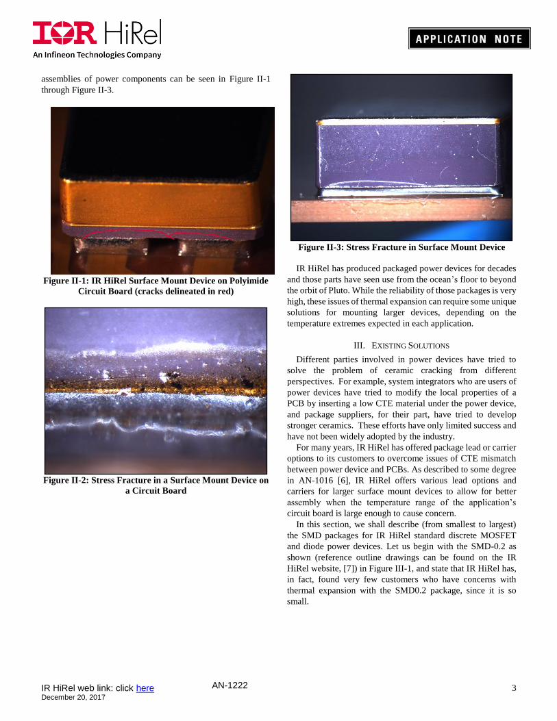
PCB’s. Some examples of fractures in finished circuit card
I
IR HiRel web link: click here December 20, 2017
3 AN-1222
assemblies of power components can be seen in Figure II-1
through Figure II-3.
Figure II-1: IR HiRel Surface Mount Device on Polyimide
Circuit Board (cracks delineated in red)
Figure II-2: Stress Fracture in a Surface Mount Device on
a Circuit Board
Figure II-3: Stress Fracture in Surface Mount Device
IR HiRel has produced packaged power devices for decades
and those parts have seen use from the ocean’s floor to beyond
the orbit of Pluto. While the reliability of those packages is very
high, these issues of thermal expansion can require some unique
solutions for mounting larger devices, depending on the
temperature extremes expected in each application.
III. EXISTING SOLUTIONS
Different parties involved in power devices have tried to
solve the problem of ceramic cracking from different
perspectives. For example, system integrators who are users of
power devices have tried to modify the local properties of a
PCB by inserting a low CTE material under the power device,
and package suppliers, for their part, have tried to develop
stronger ceramics. These efforts have only limited success and
have not been widely adopted by the industry.
For many years, IR HiRel has offered package lead or carrier
options to its customers to overcome issues of CTE mismatch
between power device and PCBs. As described to some degree
in AN-1016 [6], IR HiRel offers various lead options and
carriers for larger surface mount devices to allow for better
assembly when the temperature range of the application’s
circuit board is large enough to cause concern.
In this section, we shall describe (from smallest to largest)
the SMD packages for IR HiRel standard discrete MOSFET
and diode power devices. Let us begin with the SMD-0.2 as
shown (reference outline drawings can be found on the IR
HiRel website, [7]) in Figure III-1, and state that IR HiRel has,
in fact, found very few customers who have concerns with
thermal expansion with the SMD0.2 package, since it is so
small.
IR HiRel web link: click here December 20, 2017
4 AN-1222
Figure III-1: SMD-0.2 Outline Drawing (See IR HiRel
Web Site)
Since this SMD-0.2 device is rather small, IR HiRel has not
seen a need to provide any packaging options other than the
standard.
The next size up is the SMD-0.5, as shown [8] in Figure III-2.
Figure III-2: SMD-0.5 Outline Drawing (See IR HiRel
Web Site)
There are options for this package (and one of the subsequent
sizes) to provide strain relief in the forms of lead attachment of
ribbons of copper to the SMD package. The concept of this is
shown in Figure III-3 and the dimensions of the lead attach
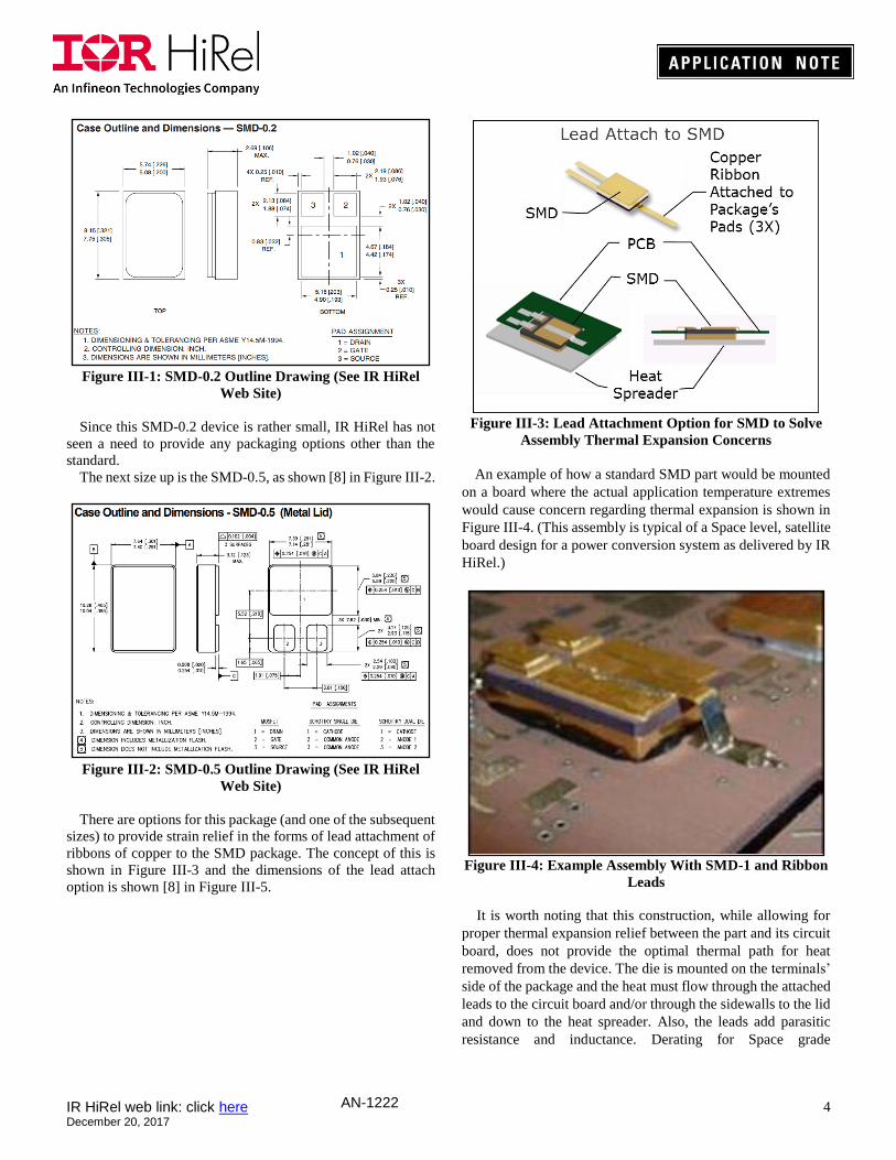
option is shown [8] in Figure III-5.
Figure III-3: Lead Attachment Option for SMD to Solve
Assembly Thermal Expansion Concerns
An example of how a standard SMD part would be mounted
on a board where the actual application temperature extremes
would cause concern regarding thermal expansion is shown in
Figure III-4. (This assembly is typical of a Space level, satellite
board design for a power conversion system as delivered by IR
HiRel.)
Figure III-4: Example Assembly With SMD-1 and Ribbon
Leads
It is worth noting that this construction, while allowing for
proper thermal expansion relief between the part and its circuit
board, does not provide the optimal thermal path for heat
removed from the device. The die is mounted on the terminals’
side of the package and the heat must flow through the attached
leads to the circuit board and/or through the sidewalls to the lid
and down to the heat spreader. Also, the leads add parasitic
resistance and inductance. Derating for Space grade
IR HiRel web link: click here December 20, 2017
5 AN-1222
components does aid in this problem, as the heat that results in
a derated application can often be sufficiently conducted in this
manner.
Figure III-5: SMD-0.5 with Leads, Outline Drawing (See
IR HiRel Web Site)
The next size larger package is the SMD-1 as shown [9] in
Figure III-6.
Figure III-6: SMD-1 Outline Drawing (See IR HiRel Web
Site)
As the reader may begin to imagine, as the size of our
packages increases, the concerns regarding thermal expansion
(and now heat removal) become more prevalent. In this package
style, not only is a lead attachment option available for thermal
expansion concerns [9] as shown in Figure III-7, but we also
have a part carrier so the heat can flow more directly down
through the bottom of the device to allow for a better thermal
path.
Figure III-7: SMD-1 with Leads, Outline Drawing (See IR
HiRel Web Site)
The concept of the part carrier is to provide a strain relief in
the leads as well as to allow the heat to flow more directly down
through the device mounting. The physical construction of the
carrier is described in a higher level in Figure III-8.
Figure III-8: Carrier for SMD
The direct bond copper substrate provides a more direct
thermal path down through the carrier. The visual
representation of an SMD part on a carrier is shown in Figure
III-9 using the next size (SMD-2) to give the reader some idea
of how large the solution has become, relative to the original
package.

IR HiRel web link: click here December 20, 2017
6 AN-1222
Figure III-9: SMD-2 on carrier
The carrier itself for an SMD-1 is described [9] in more detail
in Figure III-10.
Figure III-10: SMD-1 on Carrier, Outline Drawing (See IR
HiRel Web Site)
Finally, the largest legacy SMD discrete device package from
IR HiRel is the SMD-2. We have now arrived at the package
size which shall be compared to our newest improvement, the
SupIR-SMD, which shall be described in more detail in the next
section of this document. This device is shown [10] in Figure
III-11, with the leads and carrier options shown in Figure III-12
and Figure III-13, respectively.
Figure III-11: SMD-2 Outline Drawing (See IR HiRel Web
Site)
Figure III-12: SMD-2 with Leads, Outline Drawing (See
IR HiRel Web Site)
IR HiRel web link: click here December 20, 2017
7 AN-1222
Figure III-13: SMD-2 on Carrier, Outline Drawing (See IR
HiRel Web Site)
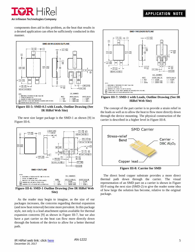
IV. THE SUPIR-SMD: A BETTER SOLUTION
Adding ribbon leads to the SMD packages and then
providing carriers for the larger SMD’s allows for solutions to
the problem of thermal expansion mismatch, but the inherent
problem lies at the terminal interface between the part and the
solder pads of the circuit board. IR HiRel has re-designed the
package itself in order to achieve a better solution for thermal
expansion and for heat transfer.
In order to solve the stress cracking problem caused by the
large CTE mismatch between power package and circuit board,
and minimize the thermal and electrical resistance as well, IR
HiRel adopted a package design with a multiple layer base as
shown in Figure IV-1. In this design, the base has two layers,
the layer that connects the ceramic body has a CTE that matches
the ceramic CTE, and the layer that connects the circuit board
has a CTE value between those of first layer and circuit board.
In this way, the CTE changes gradually from ceramic to PCB
and thus reduces the stress from a large CTE mismatch. The
idea was patented (US patent #9,559,026 [1]) by Infineon
Technologies, the parent company of IR Hirel. The new design
concept and the dimensioned drawing of the design are shown
in Figure IV-2 and Figure IV-3, respectively.
Figure IV-1: The SupIR-SMD, A New Design Concept
(Cutaway View Showing Chip and Wirebond Inside)
The new SupIR-SMD incorporates the stress relief of wide,
flat leads with a curved structure and the more direct thermal
path through the bottom of the part where the die is mounted.
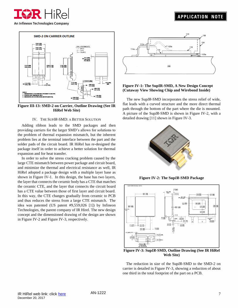
A picture of the SupIR-SMD is shown in Figure IV-2, with a
detailed drawing [11] shown in Figure IV-3.
Figure IV-2: The SupIR-SMD Package
Figure IV-3: SupIR-SMD, Outline Drawing (See IR HiRel
Web Site)
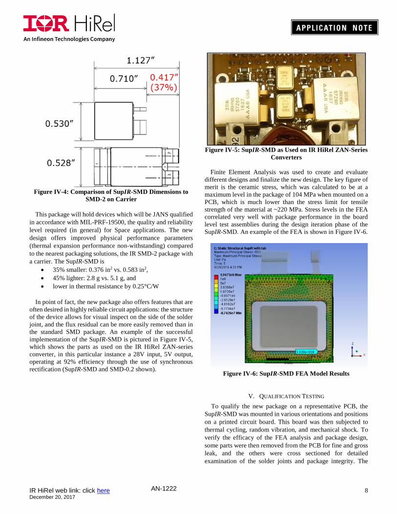
The reduction in size of the SupIR-SMD to the SMD-2 on
carrier is detailed in Figure IV-3, showing a reduction of about
one third in the total footprint of the part on a PCB.
IR HiRel web link: click here December 20, 2017
8 AN-1222
Figure IV-4: Comparison of SupIR-SMD Dimensions to
SMD-2 on Carrier
This package will hold devices which will be JANS qualified
in accordance with MIL-PRF-19500, the quality and reliability
level required (in general) for Space applications. The new
design offers improved physical performance parameters
(thermal expansion performance non-withstanding) compared
to the nearest packaging solutions, the IR SMD-2 package with
a carrier. The SupIR-SMD is
35% smaller: 0.376 in2 vs. 0.583 in2,
45% lighter: 2.8 g vs. 5.1 g, and
lower in thermal resistance by 0.25°C/W
In point of fact, the new package also offers features that are
often desired in highly reliable circuit applications: the structure
of the device allows for visual inspect on the side of the solder
joint, and the flux residual can be more easily removed than in
the standard SMD package. An example of the successful
implementation of the SupIR-SMD is pictured in Figure IV-5,
which shows the parts as used on the IR HiRel ZAN-series
converter, in this particular instance a 28V input, 5V output,
operating at 92% efficiency through the use of synchronous
rectification (SupIR-SMD and SMD-0.2 shown).
Figure IV-5: SupIR-SMD as Used on IR HiRel ZAN-Series
Converters
Finite Element Analysis was used to create and evaluate
different designs and finalize the new design. The key figure of
merit is the ceramic stress, which was calculated to be at a
maximum level in the package of 104 MPa when mounted on a
PCB, which is much lower than the stress limit for tensile
strength of the material at ~220 MPa. Stress levels in the FEA
correlated very well with package performance in the board
level test assemblies during the design iteration phase of the
SupIR-SMD. An example of the FEA is shown in Figure IV-6.
Figure IV-6: SupIR-SMD FEA Model Results
V. QUALIFICATION TESTING
To qualify the new package on a representative PCB, the
SupIR-SMD was mounted in various orientations and positions
on a printed circuit board. This board was then subjected to
thermal cycling, random vibration, and mechanical shock. To
verify the efficacy of the FEA analysis and package design,
some parts were then removed from the PCB for fine and gross
leak, and the others were cross sectioned for detailed
examination of the solder joints and package integrity. The

IR HiRel web link: click here December 20, 2017
9 AN-1222
combination of the leak tests and the cross sections were to
establish conclusive suitability of the SupIR-SMD to remain
free of any cracks formed under these demanding thermal and
mechanical conditions.
The details of the test are as follows. First, the board-level
assemblies were subjected to thermal cycling. Temperature
cycling was performed in according with MIL-STD-750F,
Method 1051 [12], with some additional constraints. This test
applied 500 temperature cycles from -55°C to 100°C with a
minimum 10°C/minute ramp and a 15 minute dwell time.
Checks were performed after these thermal cycles and the
qualification continued without any failure through the next
stage of mechanical stresses.
The next step in qualification was to take these board
assemblies and test them with respect to Random Vibration in
accordance with MIL-STD-883J with Change 5 [13], Method
2026, Condition 1J. Figure V-1 shows a picture of the setup (Z-
axis example shown) for the random vibration test with
multiple SupIR-SMD’s on the board. As per the standard, the
SupIR-SMD assemblies were vibrated in three dimensions, to a
level of 36.6 rms G’s for 15 minutes (each dimension). The
package was also tested for Mechanical Shock to 1500 G’s, in
accordance with Method 2002.5, Condition B of the same
standard. That means that the assemblies saw (at least) 1500
G’s peak for half a millisecond, and this was done five times in
each axis.
Figure V-1: Z-axis Random Vibration Setup
The measured profile of the random vibration forces is shown
in Figure V-2 (Z-axis example given). All three axis were
tested, but only one is shown for the sake of clarity.
Figure V-2: Measured Vibration Profile for Z-Axis
Figure V-3: Y-axis Mechanical Shock Setup
The measured mechanical shock is shown in Figure V-4. All
axes and orientations were tested and measured.
Figure V-4: Measured Y-axis Mechanical Shock
VI. RESULTS OF QUALIFICATION
The end results of these sequential qualification test results
are described in this section. First, fine and gross leak
IR HiRel web link: click here December 20, 2017
10 AN-1222
measurements were made in accordance with MIL-STD-750F,
Method 1071 [9]. These measurements were taken on SupIR-
SMD parts that had been removed from the board, and all of
these parts passed the test, whose purpose is to verify the
integrity of the package itself.
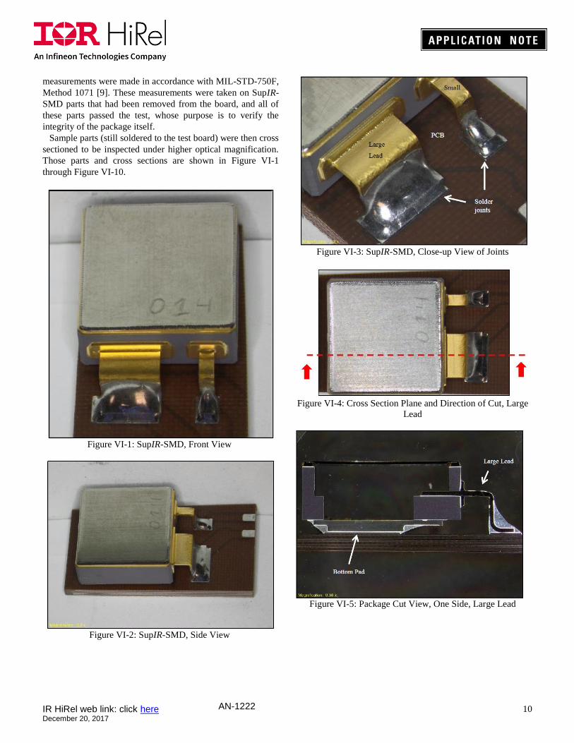
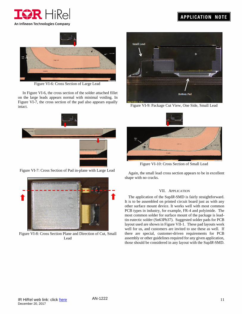
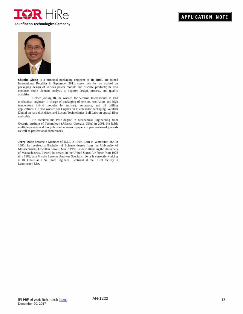
Sample parts (still soldered to the test board) were then cross
sectioned to be inspected under higher optical magnification.
Those parts and cross sections are shown in Figure VI-1
through Figure VI-10.
Figure VI-1: SupIR-SMD, Front View
Figure VI-2: SupIR-SMD, Side View
Figure VI-3: SupIR-SMD, Close-up View of Joints
Figure VI-4: Cross Section Plane and Direction of Cut, Large
Lead
Figure VI-5: Package Cut View, One Side, Large Lead
IR HiRel web link: click here December 20, 2017
11 AN-1222
Figure VI-6: Cross Section of Large Lead
In Figure VI-6, the cross section of the solder attached fillet
on the large leads appears normal with minimal voiding. In
Figure VI-7, the cross section of the pad also appears equally
intact.
Figure VI-7: Cross Section of Pad in-plane with Large Lead
Figure VI-8: Cross Section Plane and Direction of Cut, Small
Lead
Figure VI-9: Package Cut View, One Side, Small Lead
Figure VI-10: Cross Section of Small Lead
Again, the small lead cross section appears to be in excellent
shape with no cracks.
VII. APPLICATION
The application of the SupIR-SMD is fairly straightforward.
It is to be assembled on printed circuit board just as with any
other surface mount device. It works well with most common
PCB types in industry, for example, FR-4 and polyimide. The
most common solder for surface mount of the package is lead-
tin eutectic solder (Sn63Pb37). Suggested solder pads for PCB
layout used are shown in Figure VII-1. These pad layouts work
well for us, and customers are invited to use these as well. If
there are special, customer-driven requirements for PCB
assembly or other guidelines required for any given application,
those should be considered in any layout with the SupIR-SMD.

IR HiRel web link: click here December 20, 2017
12 AN-1222
Figure VII-1: SupIR-SMD Nominal, Suggested Solder
Pads (Dimensions in mm)
The cleaning of solder flux residual is also easy. The two
leads are visible and accessible, and the pedestal raises up the
package to give a clearance of at least 20 mils between the
package and PCB. This aids the process of using cleaning fluid
or vapor to carry away solder flux residual completely, which
increases the reliability of the solder joint and the device.
The product nomenclature for SupIR-SMD MOSFET
devices starts with “IRHNS”. There are diodes offered with
this technology as well, with a package designation of “NS” in
the product nomenclature.
The early adopters of the SupIR-SMD have been satisfied
with the performance of this package platform. As one of the
customers put it: “The new SupIR offering has opened up our
design to a product that can move more power with better
reliability and lower manufacturing cost.”
VIII. CONCLUSIONS
The extensive test results show that the new SupIR-SMD
package has an excellent ability to withstand thermal expansion
difference between package and printed circuit board,
maintaining the hermetic integrity of the package as well as the
solder joint from the part to a printed circuit board. In
comparison to the prior art, this new package also allows for a
significantly reduced footprint on the board, reduced weight,
and a more direct thermal path for heat transfer. Specific details
on each part offered in this package can be found in the parts’
respective product datasheets on the Infineon web site for IR
HiRel: http://www.irf.com/product/_/N~1njci1.
REFERENCES
[1] Xiong et al., US Patent Number 9,559,026 B2, January 31, 2017.
[2] The Physics Hypertextbook, Thermal Expansion, published 1998-2017, Glenn Elert, Available https://physics.info/expansion/
[3] The Engineering Tool Box: Coefficients of Thermal Expansion,
Available http://www.engineeringtoolbox.com/linear-expansion-coefficients-d_95.html
[4] FR4 PCB properties, Available
http://pdf.eicom.ru/datasheets/injectorall_pdfs/fr-4_specs/fr-4_specs.pdf [5] Chet Guiles, “Everything You Wanted To Know About Laminates”,
(Arlon Electronic Substrates: 2013), 10th Ed., Available
https://imageserv11.team-logic.com/mediaLibrary/303/Arlon_LaminatesGuide_Full_3_1.pdf, p.
60.
[6] Application Note 1016, Tiva Bussarakons, International Rectifier, Available http://www.irf.com/technical-info/appnotes/an-1016.pdf
[7] SMD-0.2 Outline Drawing, Available http://www.irf.com/package/hirel/smd02po.pdf
[8] SMD-0.5 Outline Drawing, Available http://www.irf.com/package/hirel/smd05po.pdf
[9] SMD-1 Outline Drawing, Available http://www.irf.com/package/hirel/smd1po.pdf
[10] SMD-2 Outline Drawing, Available http://www.irf.com/package/hirel/smd2po.pdf
[11] SupIR-SMD Outline Drawing, Available
http://www.irf.com/package/hirel/supirsmd2po.pdf [12] MIL-STD-750F, Available http://everyspec.com/MIL-STD/MIL-STD-
0700-0799/MIL-STD-750F_39654/
[13] MIL-STD-883J, Change Notice 5, Available http://everyspec.com/MIL-
STD/MIL-STD-0800-0899/download.php?spec=MIL-STD-883J_CHG-5.052158.pdf
Michael F. Thompson (IEEE M’05–SM’07) became a Member (M) of IEEE
in 2005, and a Senior Member (SM) in 2007. Born in Pittsburgh, PA in 1972, the author received a Bachelor of Science degree from the University of
Pennsylvania in Philadelphia, PA, USA in 1994, and a Master of Science degree
(with a specialty in power electronics and controls) from the State University of New York in 1998.
He has worked for Lockheed Martin and Northrop Grumman. His
design experience covers AC-DC, DC-AC, DC-DC power conversion at power levels that range from milliwatts to megawatts. He is familiar with the
construction and characteristics of energy storage devices and the complexities
of digital controls for power systems. Low noise output ripple designs and distributed power systems are of interest to him. He is presently working for
International Rectifier as the IR Hi-Rel Principal, Applications, for the Eastern
United States and is based out of his office in Maryland. For IR HiRel
customers who wish to contact him after reading this paper, his email address
is [email protected]. His LinkedIn profile with more details is
located here:
IR HiRel web link: click here December 20, 2017
13 AN-1222
Shunhe Xiong is a principal packaging engineer of IR Hirel. He joined
International Rectifier in September 2011, since then he has worked on packaging design of various power module and discrete products; he also
conducts finite element analysis to support design, process, and quality
activities.
Before joining IR, he worked for Vectron International as lead
mechanical engineer in charge of packaging of sensors, oscillators and high
temperature hybrid modules for military, aerospace, and oil drilling applications. He also worked for Cognex on vision senor packaging, Western
Digital on hard disk drive, and Lucent Technologies-Bell Labs on optical fiber
and cable. He received his PhD degree in Mechanical Engineering from
Georgia Institute of Technology (Atlanta, Georgia, USA) in 2001. He holds
multiple patents and has published numerous papers in peer reviewed journals as well as professional conferences.
Jerry Dube became a Member of IEEE in 1999. Born in Worcester, MA in
1960, he received a Bachelor of Science degree from the University of
Massachusetts, Lowell in Lowell, MA in 1998. Prior to attending the University of Massachusetts, Lowell, he served in the United States Air Force from 1978
thru 1982, as a Missile Systems Analysts Specialist. Jerry is currently working
at IR HiRel as a Sr. Staff Engineer, Electrical at the HiRel facility in
Leominster, MA.


![Hi-Rel Electronics [MA HiRel]](https://img.pdfslide.net/doc/110x75/627c6dfb6f7bcb24784371d3/hi-rel-electronics-ma-hirel.jpg)