Embed Size (px)
Citation preview
Application Note AN-51 HiperTFS Family
www.powerint.com March 2013
Design Considerations
™
Figure 1. A Simplified Schematic of HiperTFS With PC Main Supply With 3.3 V, 5 V, 12 V, -12 V and One +5 V Standby Output.
Introduction
The HiperTFS is highly integrated, very efficient integrated offline switcher IC mainly intended for PC main and standby applications. The IC includes the control, drivers and switches for a two-switch forward high power main converter and the control and power switch for a flyback standby converter. A minimal count of external components are required for full operation. The HiperTFS package (eSIP-16B) requires no electrical isolation of the exposed back tab, enabling direct mounting to a heat sink for maximally effective heat sinking and minimal mounting hardware. The HiperTFS series covers a range from 170 W to 415 W continuous power output (at 25 °C ambient) and in applications such as PC power supplies which require very dense and compact layout and high efficiency. HiperTFS provides significant advantages to the designer whether it be for 70 PLUS, 80 PLUS or 80 PLUS Bronze compliant designs.
The main forward converter is intended to work with a PFC boost front end provides a regulated voltage from 290 VDC to 420 VDC input (385 VDC typical). The standby section of HiperTFS is intended for wide range operation from 100 VDC to 420 VDC. High efficiency is made possible by using an asymmetrical version of the two-switch forward which allows an operating duty cycle greater than 50%, hence lower RMS switch currents and lower output diode voltage ratings. A proprietary protection circuit guarantees safe operation by limiting the forward
transformer single cycle flux and guaranteeing transformer reset, eliminating transformer saturation under all conditions. Special functions include OVP latch for standby, remote-ON/OFF capability for the main converter, programmable maximum primary current limit ranges for main and standby supplies, frequency jitter for low EMI, and flat standby output overload characteristics with respect to input voltage.
Basic Circuit Configuration
The circuit shown in Figure 1 shows the basic configuration of a PC power supply design using HiperTFS, including main and standby converters. The high level of integration of HiperTFS, provides many of the needed functions that would otherwise require external circuitry saving development time and material costs. One common external circuit configuration is useful for a range of applications. Advanced features like line undervoltage and overvoltage protection, reset and flux density limiter for main transformer, external current limit selection, start-up features, and remote-ON/OFF are easily implemented with a minimal number of external components.
Other application specific issues such as constant current, and constant power outputs, etc. are beyond the scope of this design guide. However, if required such specifications may be satisfied by adding additional circuitry to the basic converter configuration.
HD
14 - 25 V
14 - 20 V
HS
85 - 265VAC
380 VDC
MainON/OFF RTN
RTN
+5 VStandby
MainControl
StandbyControl
FB
FB
EN
EN
TSTANDBY
TMAIND
G S
HiperTFS VDDH
R
L
FB
EN
BP
DSB
PI-6004-092910
PFCBoost
+
CONTROL
Post Reg
+12 V
-12 V
+3.3 V
+5 V
Rev. A 03/13
2
Application Note
www.powerint.com
AN-51
Scope
This application note is intended for engineers designing an isolated AC-DC forward power supply with flyback standby using the HiperTFS family of devices. It is assume that there is a power factor converter boost stage (HiperPFS) providing 385 VDC to the input of the main converter. The standby converter must operate with the PFC boost stage both on or off so the standby has a wide DC operating input range of 100 VDC to 420 VDC. For detailed information on PFC stage refer to HiperPFS application note. Guidelines and a step-by-step walk through of the HiperTFS design spreadsheet are given to enable an engineer to quickly select key components and design a suitable main transformer, standby transformer and main output inductor design for a PC power supply. This application note refers directly to the PIXls design spreadsheet that is part of the PI Expert™ design software suite. The basic configuration used in PC power supply is shown in Figure 1, which also serves as the reference circuit for component identifications used in the description throughout this application note.
In addition to this application note the reader may also find the HiperTFS Reference Design Kit (RDK-249) containing an engineering prototype board, engineering report and device samples useful as an example of a working power supply. There is also an engineering report available describing a full multiple output design for PC main applications. Further details on downloading PI Expert, obtaining a RDK and updates to this document can be found at www.powerint.com.
Overview of Design Method
Readers needing to start immediately can use the following information to quickly design the transformer and select the components for a first prototype. The information described below needs to be entered into the PIXls design spreadsheet. Other parameters will be automatically selected based on a typical design. References to spreadsheet cell locations are provided in square brackets [cell reference].
Design Using PIXls
Description of PIXls FormatThere are four major sections in this spreadsheet:1. Input parameters and device selection and device
configuration.2. Transformer core selection and winding design for main
forward converter.3. Output coupled inductor core size and core material
selection and winding design for main forward.4. Standby transformer design.
Each of these sections have grayed cells that are locations for user enterable parameters. When PIXls is first opened these grayed cells will contain default values already entered for a typical 300 W output main 17 W output standby design. The designer is advised to leave these cells unchanged unless they have more precise information.
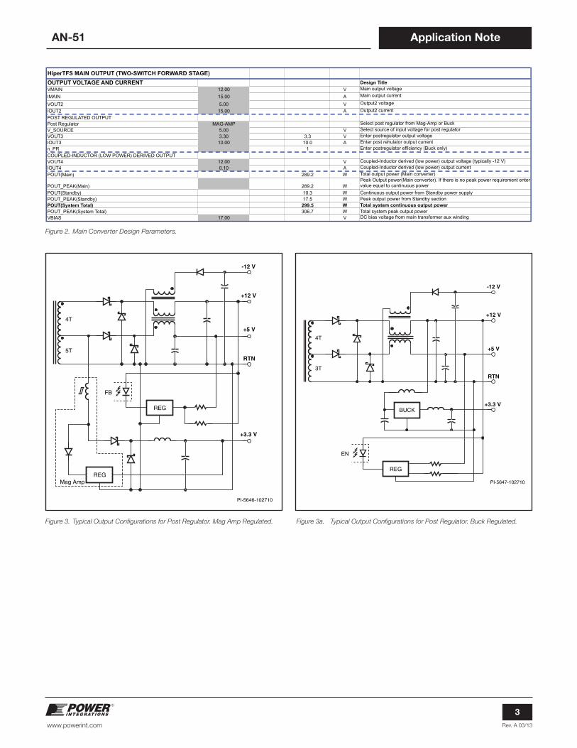
Output Voltages and Currents of Main Converter
There are commonly four output voltages provided by a PC main converter. These are +5 V, +12 V, +3.3 V and -12 V. The main transformer usually has only two output windings which source the +5 V and +12 V outputs. The outputs of these two windings are rectified and drive the input of a coupled main output inductor. The third output, commonly a 3.3 V output, is derived from a switching post regulator, which is typically a mag amp sourced from the +5 V winding or a synchronous buck converter sourced from the +12 V output. Finally, there is commonly a -12 V output sourced from a flyback winding on the coupled output inductor (intended for light loads only).
Section 1 – Input Parameters, Device Selection and Device Configuration
Step 1 – Enter Output Current and Voltages*note brackets[ ] indicate actual spreadsheet nameparentheses( ) indicates typical value
• Enter output current and voltage values for [VMAIN] and [IMAIN] (+12 V).
*note - VMAIN is highest power output.• Enter output current and voltage values for [VOUT2] and
[IOUT2] (+5 V).• Enter output current and voltage values for post regulator
[VOUT3] and [IOUT3] (+3.3 V).• Select type of post regulation[Post Regulator] (MAG AMP,
Buck or NONE).• If buck post regulator is selected enter estimated efficiency of
buck stage [n_PR]. This is ignored if MAG AMP was chosen.• Enter voltage and current of inductor derived output (-12 V),
[VOUT4] and [IOUT4].• [POUT(MAIN)] is the total maximum output power of the main
converter which is the sum of the output power of all main converter outputs.
• If there is a peak power requirement then enter the peak power in [POUT_PEAK(MAIN)]. The additional power over continuous maximum output power is assumed to be sourced from VMAIN.
• [POUT(STANDBY)] and [POUT_PEAK(STANDBY)] have default values entered These will later change when entering actual standby output power in standby section of spreadsheet.
• [VBIAS] is typically 17 V which is used for bias support of HiperTFS bootstrap high-side drive, and the source for the +12 V regulator which is used for remote, ON/OFF and bias for HiperPFS boost controller. Changing the target voltage of VBIAS could be detrimental to supply performance.
Rev. A 03/13
3
Application Note
www.powerint.com
AN-51
Figure 2. Main Converter Design Parameters.
Figure 3. Typical Output Configurations for Post Regulator. Mag Amp Regulated. Figure 3a. Typical Output Configurations for Post Regulator. Buck Regulated.
PI-5646-102710
REG
Mag Amp
FB
4T
5T
REG
-12 V
+12 V
+5 V
RTN
+3.3 V
HiperTFS MAIN OUTPUT (TWO-SWITCH FORWARD STAGE)
OUTPUT VOLTAGE AND CURRENT Design Title
VMAIN 12.00 V Main output voltage
IMAIN 15.00 A Main output current
VOUT2 5.00 V Output2 voltage
IOUT2 15.00 A Output2 current
POST REGULATED OUTPUTPost Regulator MAG-AMP Select post regulator from Mag-Amp or Buck
V_SOURCE 5.00 V Select source of input voltage for post regulator
VOUT3 3.30 3.3 V Enter postregulator output voltage
IOUT3 10.00 10.0 A Enter post rehulator output current
n_PR 1 Enter postregulator efficiency (Buck only)
COUPLED-INDUCTOR (LOW POWER) DERIVED OUTPUTVOUT4 12.00 V Coupled-Inductor derived (low power) output voltage (typically -12 V)
IOUT4 0.10 A Coupled-Inductor derived (low power) output current
POUT(Main) 289.2 W Total output power (Main converter)
POUT_PEAK(Main) 289.2 WPeak Output power(Main converter). If there is no peak power requirement enter value equal to continuous power
POUT(Standby) 10.3 W Continuous output power from Standby power supplyPOUT_PEAK(Standby) 17.5 W Peak output power from Standby sectionPOUT(System Total) 299.5 W Total system continuous output powerPOUT_PEAK(System Total) 306.7 W Total system peak output powerVBIAS 17.00 V DC bias voltage from main transformer aux winding
PI-5647-102710
REG
EN
4T
3T
-12 V
+12 V
+5 V
RTN
+3.3 VBUCK
Rev. A 03/13
4
Application Note
www.powerint.com
AN-51
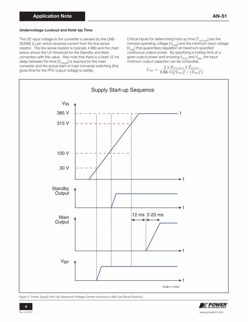
Undervoltage Lockout and Hold-Up Time
The DC input voltage to the converter is sensed by the LINE-SENSE (L) pin which receives current from the line sense resistor. The line sense resistor is typically 4 MW and the chart below shows the UV threshold for the Standby and Main converters with this value. Also note that there is a fixed 12 ms delay between the time [VOV(ON)] is reached for the main converter and the actual start of main converter switching (this gives time for the PFC output voltage to settle).
Figure 4. Power Supply Start-Up Sequence (Voltages Shown Assume a 4 MW Line Sense Resistor).
Critical inputs for determining hold-up time [THOLDUP] are the nominal operating voltage [VNOM] and the minimum input voltage [VMIN] that guarantees regulation at maximum specified continuous output power. By specifying a holdup time at a given output power and knowing VNOM and VMIN, the input minimum output capacitor can be computed.
.C
VP T
V0 862 _
MINNOM
OUT TOTAL HOLDUP
MIN2 2#
# #=
-^ ^^ h h h
VIN
Supply Start-up Sequence
StandbyOutput
MainOutput
VBP
12 ms
385 V
315 V
100 V
t
t
t
t
t
30 V
2-20 ms
PI-5611-111910
Rev. A 03/13
5
Application Note
www.powerint.com
AN-51
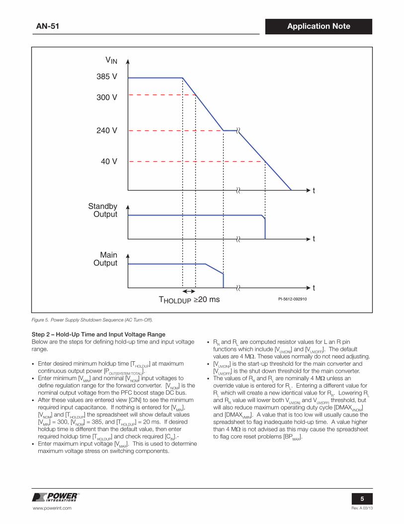
Figure 5. Power Supply Shutdown Sequence (AC Turn-Off).
Step 2 – Hold-Up Time and Input Voltage RangeBelow are the steps for defining hold-up time and input voltage range.
• Enter desired minimum holdup time [THOLDUP] at maximum continuous output power [POUT(SYSTEM TOTAL)].
• Enter minimum [VMIN] and nominal [VNOM] input voltages to define regulation range for the forward converter. [VNOM] is the nominal output voltage from the PFC boost stage DC bus.
• After these values are entered view [CIN] to see the minimum required input capacitance. If nothing is entered for [VMIN], [VNOM] and [THOLDUP] the spreadsheet will show default values [VMIN] = 300, [VNOM] = 385, and [THOLDUP] = 20 ms. If desired holdup time is different than the default value, then enter required holdup time [THOLDUP] and check required [CIN].-
• Enter maximum input voltage [VMAX]. This is used to determine maximum voltage stress on switching components.
VIN
StandbyOutput
MainOutput
385 V
300 V
240 V
40 V
t
t
tPI-5612-092910THOLDUP ≥20 ms
• RR and RL are computed resistor values for L an R pin functions which include [VUV(ON)] and [VUV(OFF)]. The default values are 4 MW. These values normally do not need adjusting.
• [VUV(ON)] is the start-up threshold for the main converter and [VUV(OFF)] is the shut down threshold for the main converter.
• The values of RR and RL are nominally 4 MW unless an override value is entered for RL. Entering a different value for RL which will create a new identical value for RR. Lowering RL and RR value will lower both VUV(ON) and VUV(OFF) threshold, but will also reduce maximum operating duty cycle [DMAXVNOM] and [DMAXVMIN]. A value that is too low will usually cause the spreadsheet to flag inadequate hold-up time. A value higher than 4 MW is not advised as this may cause the spreadsheet to flag core reset problems [BPMAX].
Rev. A 03/13
6
Application Note
www.powerint.com
AN-51
Step 3 – Selecting HiperTFS Device, Current Limit Setting and KDI Goal and Clamp Selection
There are several HiperTFS devices available in the family. The appropriate device depends on the output power, type of application and thermal environment. For example in PC power supplies two different ambient requirements are commonly used. Original equipment manufacturer (OEM) power output is specified at 50 °C ambient where as clones typically are specified at 25 °C ambient. Table 1 shows which device is best suited for a given ambient temperature. There is also the option to select one of three current limit values. Selection is made by entering a value for KI [KI] of either 1, 0.8 or 0.6. These values correspond to the data sheet parameters ILIM(3)MA, ILIM(2)MA and ILIM(1)MA respectively. The resultant minimum device current limit is shown in cell [ILIMITSELECT]. Implementing the selected KI is achieved by selecting the value of pull-up resistor from the FEEDBACK to the BYPASS pin of the HiperTFS device. [RFB] shows the appropriate value for the pull-up resistor for the selected KI. Table 2 shows the relationship between IFB and selected current limit.
For a two-switch Forward topology, power is delivered during the on-time of the main switches. During the off-time, both leakage and magnetizing energy in the main transformer must
Figure 6. Power Supply Under/Overvoltage and Input Capacitor Parameters.
Output Power Table
Part NumberPOUT
TA = 25 °CPOUT
TA = 50 °CPOUT
PKPOUT
Standby
TFS757HG 193 W 163 W 228 W 20 W
TFS758HG 236 W 200 W 278 W 20 W
TFS759HG 280 W 235 W 309 W 20 W
TFS760HG 305 W 258 W 358 W 20 W
TFS761HG 326 W 276 W 383 W 20 W
TFS762HG 360 W 304 W 407 W 20 W
TFS763HG 388 W 327 W 455 W 20 W
TFS764HG 414 W 344 W 530 W 20 W
Table 1. HiperTFS Output Power Table.
be reset and recovered in a safe manner. There are two options for main transformer reset within [CLAMP SELECTION]: clamp-to-rail and clamp-to-ground (see Figure 7 for both clamp schematics). Clamp-to-rail clamps the bottom main switch to a constant value above the input DC bus (385 VDC). This is the simplest and least expensive clamp method and also has the convenience of allowing the standby converter to share the clamp network. Clamp-to-ground is the second option which creates a constant reset voltage with respect to primary ground and has the advantage of allowing wider nominal operating duty cycle, which offers either the advantage of lower RMS current for the primary main switches of HiperTFS or allows the use of a smaller input bulk capacitor. The default nominal duty cycle [DVNOM] for clamp-to-rail is 0.45 and the default for clamp-to-ground is 0.49.
Step 4 – Spreadsheet Procedure for Device Selection and Configuration
• Review the output power table and decide appropriate HiperTFS device depending on application, ambient tempera-ture and output power.
• Select HiperTFS device [DEVICE] from drop down list.• Selected HiperTFS device and key device parameters are
displayed [Line 42-48].• Select primary current limit factor [KI]. 1, 0.8, 0.6. [ILIMIT]
default value is 1.• The default nominal operating duty cycle is 45% for clamp-to-
rail. Notice from Figure 7 the circuit includes a 150 V Zener. This allows a maximum duty cycle at VMIN to be greater than 58% for the example spreadsheet shown. [DMAX VMIN] is typically 60% for clamp-to-rail setting. The value of the clamp Zener is selectable; however, a value range from 130 V to 150 V is advised. Care should be taken when entering a duty cycle higher than 45% for clamp-to-rail as it may cause a THOLDUP warning. Generally higher nominal operating duty cycles require changing the clamp mode to clamp-to-ground to increase reset voltage across transformer during brownout. A nominal operating duty cycle of up to 50% can be achieved with clamp-to-ground. The default value of [VCLAMP] in clamp-to-ground configuration is 530 V.
Another option to allow higher operating duty cycle is to raise VMIN for the same holdup time and use a higher CIN value. Note that in both configurations of clamp circuit DR1 is a slow recovery diode (1N4007G) which allows recycling of the magnetizing and leakage energy. A 1N4007G which is glass passivated is preferred over 1N4007 because it has well controlled reverse recovery characteristics. Using a slow recovery diode rather than a fast recovery type increases overall
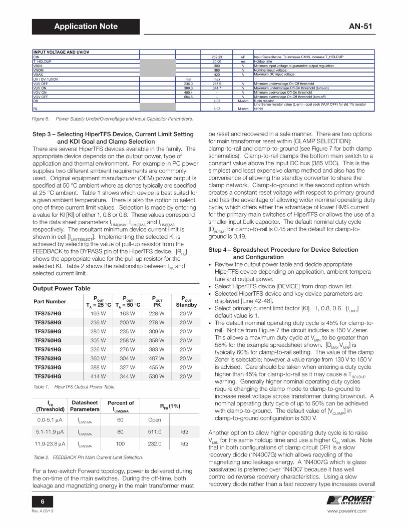
INPUT VOLTAGE AND UV/OVCIN 262.23 uF Input Capacitance. To increase CMIN, increase T_HOLDUPT_HOLDUP 20.00 ms Holdup timeVMIN 300 V Minimum input voltage to guarantee output regulationVNOM 380 V Nominal input voltageVMAX 420 V Maximum DC input voltage
UV / OV / UVOV min maxVUV OFF 236.0 287.9 V Minimum undervoltage On-Off thresholdVUV ON 300.0 344.7 V Maximum undervoltage Off-On threshold (turn-on)VOV ON 480.4 - V Minimum overvoltage Off-On thresholdVOV OFF 664.5 - V Minimum overvoltage On-Off threshold (turn-off)RR 4.03 M-ohm R pin resistor
RL 4.03 M-ohmLine Sense resistor value (L-pin) - goal seek (VUV OFF) for std 1% resistor series
Table 2. FEEDBACK Pin Main Current Limit Selection.
IFB
(Threshold)Datasheet
ParametersPercent of
ILIM(3)MA
RFB (1%)
0.0-5.1 mA ILIM(1)MA 60 Open
5.1-11.9 mA ILIM(2)MA 80 511.0 kW
11.9-23.8 mA ILIM(3)MA 100 232.0 kW
Rev. A 03/13
7
Application Note
www.powerint.com
AN-51
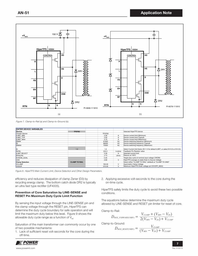
Figure 7. Clamp-to-Rail (a) and Clamp-to-Ground (b).
(a) (b)
Figure 8. HiperTFS Main Current Limit, Device Selection and Other Design Parameters.
efficiency and reduces dissipation of clamp Zener (D3) by recycling energy clamp. The bottom catch diode DR2 is typically an ultra fast type rectifier (UF4005).
Prevention of Core Saturation by LINE-SENSE and RESET Pin Maximum Duty Cycle Limit Function
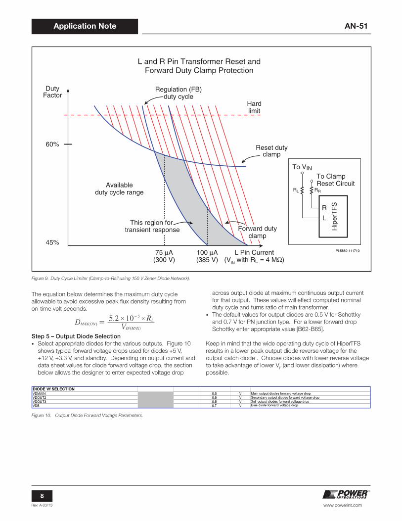
By sensing the input voltage through the LINE-SENSE pin and the clamp voltage through the RESET pin, HiperTFS can determine the duty cycle boundary for safe operation and will limit the maximum duty below this level. Figure 9 shows the allowable duty cycle range as a function of VIN.
Saturation of the main transformer can commonly occur by one of two possible mechanisms:1. Lack of sufficient reset volt-seconds for the core during the
off-time.
2. Applying excessive volt-seconds to the core during the on-time cycle.
HiperTFS safely limits the duty cycle to avoid these two possible conditions.
The equations below determine the maximum duty cycle allowed by LINE-SENSE and RESET pin limiter for reset of core.
Clamp-to-Rail:
Clamp-to-Ground:
ENTER DEVICE VARIABLESDevice TFS762 Selected HiperTFS deviceChosen Device TFS762ILIMIT_MIN 3.26 A Device current limit (Minimum)ILIMIT_TYP 3.50 A Device current limit (Typical)ILIMIT_MAX 3.75 A Device current limit (Maximum)fSMIN 61500 Hz Device switching frequency (Minimum)fS 66000 Hz Device switching frequency (Typical)fSMAX 70500 Hz Device switching frequency (Maximum)
KI 1.0 1.0 Select Current limit factor (KI=1.0 for default ILIMIT, or select KI=0.8 or KI=0.6) R(FB) 232.0 k-ohms Feedback Pin Resistor valueILIMIT SELECT 3.26 A Selected current limitRDS(ON) 2.73 ohms Rds(on) at 100'C
DVNOM_GOAL 0.45 Target duty cycle at nominal input voltage (VNOM)VDS 4.80 V HiperTFS average on-state Drain to Source VoltageClamp Selection CLAMP TO RAIL Select either "CLAMP TO RAIL" (default) or "CLAMP TO GND" VCLAMP 150.00 V Asymmetric Clamp VoltageVDSOP 570.00 V Maximum HiperTFS Drain voltage (at VOVOFF_MAX)
HD
HS
D
G S
HiperTFS VDDH
R
DR1
150 V+VBUS
RTNDR2
L
FB
EN
BP
DSB
PI-5846-111810
CONTROL HD
HS
D
G S
HiperTFS VDDH
R
L
FB
EN
BP
DSB
PI-6078-111810
DR1
DR2
CONTROL
+VBUS
RTN
DV V VV V V2_MAX FORWARD VMIN
MIN DS CLAMP
CLAMP MIN DS=
- ++ -
^^
^h
hh
DV V V
V_MAX RESET VMIN
MIN DS CLAMP
CLAMP=- +^
^h
h
Rev. A 03/13
8
Application Note
www.powerint.com
AN-51
The equation below determines the maximum duty cycle allowable to avoid excessive peak flux density resulting from on-time volt-seconds.
Step 5 – Output Diode Selection • Select appropriate diodes for the various outputs. Figure 10
shows typical forward voltage drops used for diodes +5 V, +12 V, +3.3 V, and standby. Depending on output current and data sheet values for diode forward voltage drop, the section below allows the designer to enter expected voltage drop
Figure 9. Duty Cycle Limiter (Clamp-to-Rail using 150 V Zener Diode Network).
Figure 10. Output Diode Forward Voltage Parameters.
across output diode at maximum continuous output current for that output. These values will effect computed nominal duty cycle and turns ratio of main transformer.
• The default values for output diodes are 0.5 V for Schottky and 0.7 V for PN junction type. For a lower forward drop Schottky enter appropriate value [B62-B65].
Keep in mind that the wide operating duty cycle of HiperTFS results in a lower peak output diode reverse voltage for the output catch diode . Choose diodes with lower reverse voltage to take advantage of lower VF (and lower dissipation) where possible.
DIODE Vf SELECTIONVDMAIN 0.5 V Main output diodes forward voltage drop VDOUT2 0.5 V Secondary output diodes forward voltage drop VDOUT3 0.5 V 3rd output diodes forward voltage drop VDB 0.7 V Bias diode forward voltage drop
# #.DV
R5 2 10( )
MAX ONIN MAX
L5
=-
^ h
PI-5880-111710
Regulation (FB)duty cycle
Reset dutyclamp
Hardlimit
To VIN
To Clamp Reset CircuitAvailable
duty cycle range
DutyFactor
60%
RL RR
45%
100 µA(385 V)
75 µA(300 V)
L Pin Current(VIN with RL = 4 MΩ)
L and R Pin Transformer Reset andForward Duty Clamp Protection
R
L
Hip
erT
FS
Forward dutyclamp
This region for transient response
Rev. A 03/13
9
Application Note
www.powerint.com
AN-51
Figure 11. Main Transformer Core Parameters.
Figure 12. Main Transformer Flux Density and Other Parameters.
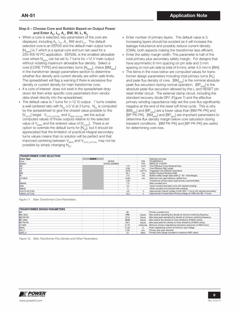
Step 6 – Choose Core and Bobbin Based on Output Power and Enter AE, LE, AL, BW, M, L, NS
• When a core is selected, key parameters of the core are displayed, including AE, LE, AL, BW and LG. The default selected core is an EER35 and the default main output turns [NMAIN] is 7 which is a typical core and turn set used for a 250-400 W PC application. EER28L is the smallest allowable core where NMAIN can be set to 7 turns for +12 V main output without violating maximum allowable flux density. Select a core [CORE TYPE] and secondary turns [NMAIN], check [BMMAX] in the transformer design parameters section to determine whether flux density and current density are within safe limits. The spreadsheet will flag a warning if there is excessive flux density or current density for main transformer core.
• If a core of interest does not exist in the spreadsheet drop down list then enter specific core parameters from vendor data sheet directly into the spreadsheet.
• The default value is 7 turns for (+12 V) output. 7 turns creates a well centered ratio with NS2 (+5 V) at 3 turns. NS2 is computed by the spreadsheet to give the closest value possible to the [VOUT2] target. VOUT2_ACTUAL and VBIAS_ACTUAL are the actual computed values of those outputs relative to the selected value of VMAIN and the entered value of [VOUT2]. There is an option to override the default turns for [NS2], but it should be appreciated that the limitation of practical integral secondary turns values means that no solution will be perfect and that improved centering between VMAIN and VOUT2_ACTUAL may not be possible by simply changing NS2.
• Enter number of primary layers. The default value is 3. Increasing layers should be avoided as it will increase the leakage inductance and possibly reduce current density (CMA), both aspects making the transformer less efficient.
• Enter the safety margin width. This parameter is half of the total primary plus secondary safety margin. For designs that have asymmetric 6 mm spacing on pin side and 3 mm spacing on non-pin side (a total of 9 mm), enter 4.5 mm in [BW].
• The items in the rows below are computed values for trans-former design parameters including total primary turns [NP] and peak flux density of core. [BMMAX] is the nominal absolute peak flux excursion during normal operation. [BPMAX] is the absolute peak flux excursion allowed by the L and RESET pin reset limiter circuit. The external clamp circuit, including the standard recovery diode DR1 (Figure 7) and the effective primary winding capacitance help set the core flux significantly negative at the end of the reset (off-time) cycle. This is why [BMMAX] and [BPMAX] are a lower value than [BM PK-PK] and [BP PK-PK]. [BMMAX] and [BPMAX] are important parameters to determine flux density margin below core saturation during transient conditions. [BM PK-PK] and [BP PK-PK] are useful for determining core loss.
TRANSFORMER CORE SELECTIONCore Type EER35 Selected core typeCore EER35 P/N: PC40EER35-ZBobbin EER35_BOBBIN P/N: BEER-35-1116CPHAE 1.07 cm^2 Core Effective Cross Sectional AreaLE 9.08 cm Core Effective Path LengthAL 2770 nH/T^2 Ungapped Core Effective InductanceBW 26.1 mm Bobbin Physical Winding WidthM 4.5 mm Bobbin safety margin tape width (2 * M = Total Margin)LG MAX 0.002 mm Maximum zero gap tolerance, default 2umL 3.00 Transformer primary layers (split primary recommended)NMAIN 7.0 Main rounded turnsNS2 3.0 Vout2 rounded secondary turns (AC stacked winding)NBIAS 5 VBias rounded turns (forward bias winding)VOUT2 ACTUAL 4.9 V Approximate Output2 voltage of with NS2 = 3 turns (AC stacked secondary)VBIAS_ACTUAL 16.2 V Approximate Forward Bias Winding Voltage at VMIN with NB = 5 turns
TRANSFORMER DESIGN PARAMETERSNP 89 Primary rounded turnsBM_MAX 1791 Gauss Max positive operating flux density at minimum switching frequencyBM PK-PK 2714 Gauss Max peak-peak operating flux density at minimum switching frequencyBP_MAX 2310 Gauss Max positive flux density at Vmax (limited by DVMAX clamp)BP PK-PK 3501 Gauss Max peak-peak flux density at Vmax (limited by DVMAX clamp)LP MIN 21.07 mHenries Minimum primary magnetizing inductance (assumes LG MAX=2um)IMAG 0.122 A Peak magnetizing current at minimum input voltageOD_P 0.58 mm Primary wire outer diameterAWG_P 23 AWG Primary Wire Gauge (rounded to maximum AWG value)
Rev. A 03/13
10
Application Note
www.powerint.com
AN-51
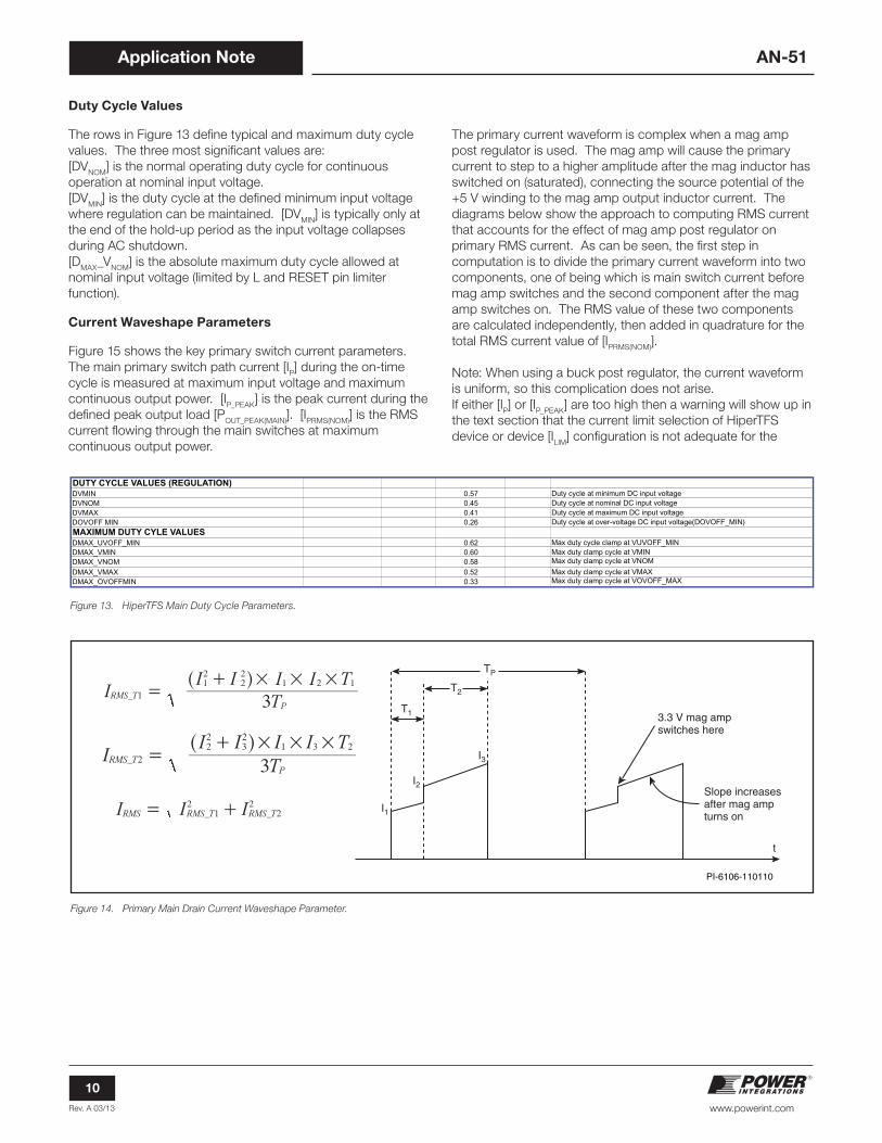
Duty Cycle Values
The rows in Figure 13 define typical and maximum duty cycle values. The three most significant values are:[DVNOM] is the normal operating duty cycle for continuous operation at nominal input voltage.[DVMIN] is the duty cycle at the defined minimum input voltage where regulation can be maintained. [DVMIN] is typically only at the end of the hold-up period as the input voltage collapses during AC shutdown.[DMAX_VNOM] is the absolute maximum duty cycle allowed at nominal input voltage (limited by L and RESET pin limiter function).
Current Waveshape Parameters
Figure 15 shows the key primary switch current parameters. The main primary switch path current [IP] during the on-time cycle is measured at maximum input voltage and maximum continuous output power. [IP_PEAK] is the peak current during the defined peak output load [POUT_PEAK(MAIN)]. [IPRMS(NOM)] is the RMS current flowing through the main switches at maximum continuous output power.
The primary current waveform is complex when a mag amp post regulator is used. The mag amp will cause the primary current to step to a higher amplitude after the mag inductor has switched on (saturated), connecting the source potential of the +5 V winding to the mag amp output inductor current. The diagrams below show the approach to computing RMS current that accounts for the effect of mag amp post regulator on primary RMS current. As can be seen, the first step in computation is to divide the primary current waveform into two components, one of being which is main switch current before mag amp switches and the second component after the mag amp switches on. The RMS value of these two components are calculated independently, then added in quadrature for the total RMS current value of [IPRMS(NOM)].
Note: When using a buck post regulator, the current waveform is uniform, so this complication does not arise.If either [IP] or [IP_PEAK] are too high then a warning will show up in the text section that the current limit selection of HiperTFS device or device [ILIM] configuration is not adequate for the
Figure 13. HiperTFS Main Duty Cycle Parameters.
Figure 14. Primary Main Drain Current Waveshape Parameter.
DUTY CYCLE VALUES (REGULATION)DVMIN 0.57 Duty cycle at minimum DC input voltage DVNOM 0.45 Duty cycle at nominal DC input voltageDVMAX 0.41 Duty cycle at maximum DC input voltage DOVOFF MIN 0.26 Duty cycle at over-voltage DC input voltage(DOVOFF_MIN)
MAXIMUM DUTY CYLE VALUESDMAX_UVOFF_MIN 0.62 Max duty cycle clamp at VUVOFF_MIN DMAX_VMIN 0.60 Max duty clamp cycle at VMINDMAX_VNOM 0.58 Max duty clamp cycle at VNOM
DMAX_VMAX 0.52 Max duty clamp cycle at VMAXDMAX_OVOFFMIN 0.33 Max duty clamp cycle at VOVOFF_MAX
ITP
TI
3
I_RMS T
12
22
1 2 1
1
# # #=
+^ h I I
PI-6106-110110
IT
I TI I I
3_RMS T
P2
22
32
1 3 2# # #=
+^ h
I I I_ _RMS RMS T RMS T12
22= +
T2
TP
t
I3
I2
I1
T1 3.3 V mag amp switches here
Slope increasesafter mag ampturns on
Rev. A 03/13
11
Application Note
www.powerint.com
AN-51
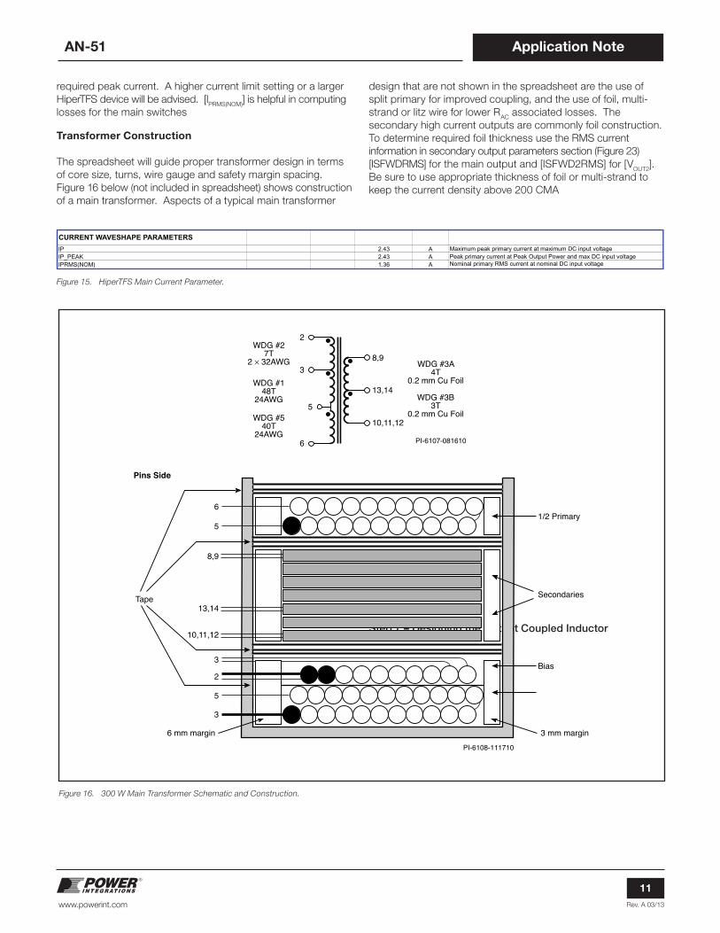
Figure 15. HiperTFS Main Current Parameter.
Figure 16. 300 W Main Transformer Schematic and Construction.
required peak current. A higher current limit setting or a larger HiperTFS device will be advised. [IPRMS(NOM)] is helpful in computing losses for the main switches
Transformer Construction
The spreadsheet will guide proper transformer design in terms of core size, turns, wire gauge and safety margin spacing. Figure 16 below (not included in spreadsheet) shows construction of a main transformer. Aspects of a typical main transformer
design that are not shown in the spreadsheet are the use of split primary for improved coupling, and the use of foil, multi-strand or litz wire for lower RAC associated losses. The secondary high current outputs are commonly foil construction. To determine required foil thickness use the RMS current information in secondary output parameters section (Figure 23) [ISFWDRMS] for the main output and [ISFWD2RMS] for [VOUT2]. Be sure to use appropriate thickness of foil or multi-strand to keep the current density above 200 CMA
Step 7 – Designing the Output Coupled Inductor
CURRENT WAVESHAPE PARAMETERS
IP 2.43 A Maximum peak primary current at maximum DC input voltageIP_PEAK 2.43 A Peak primary current at Peak Output Power and max DC input voltageIPRMS(NOM) 1.36 A Nominal primary RMS current at nominal DC input voltage
WDG #27T
2 × 32AWG WDG #3A4T
0.2 mm Cu Foil
WDG #3B3T
0.2 mm Cu Foil
WDG #148T
24AWG
WDG #540T
24AWG
3
5
6
8,9
13,14
10,11,12
PI-6107-081610
2
PI-6108-111710
Secondaries
Bias
Tape
3 mm margin
Pins Side
6 mm margin
8,9
5
6
13,14
10,11,12
3
5
2
3
1/2 Primary
Rev. A 03/13
12
Application Note
www.powerint.com
AN-51
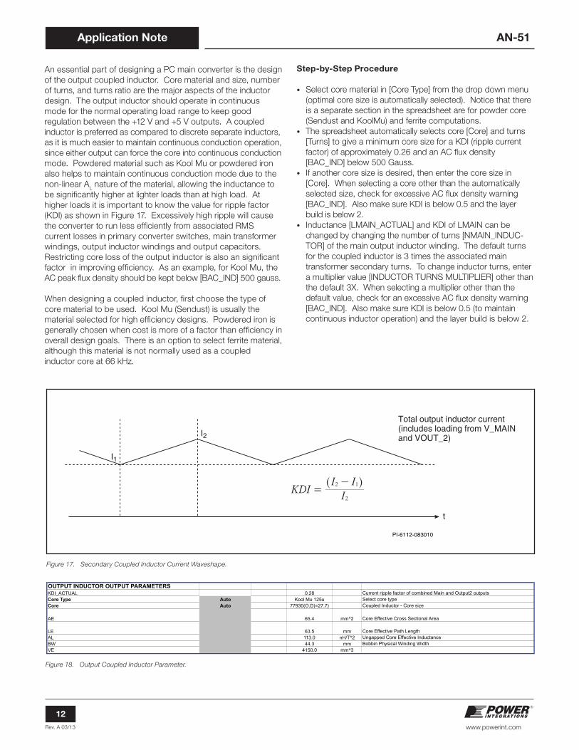
An essential part of designing a PC main converter is the design of the output coupled inductor. Core material and size, number of turns, and turns ratio are the major aspects of the inductor design. The output inductor should operate in continuous mode for the normal operating load range to keep good regulation between the +12 V and +5 V outputs. A coupled inductor is preferred as compared to discrete separate inductors, as it is much easier to maintain continuous conduction operation, since either output can force the core into continuous conduction mode. Powdered material such as Kool Mu or powdered iron also helps to maintain continuous conduction mode due to the non-linear AL nature of the material, allowing the inductance to be significantly higher at lighter loads than at high load. At higher loads it is important to know the value for ripple factor (KDI) as shown in Figure 17. Excessively high ripple will cause the converter to run less efficiently from associated RMS current losses in primary converter switches, main transformer windings, output inductor windings and output capacitors. Restricting core loss of the output inductor is also an significant factor in improving efficiency. As an example, for Kool Mu, the AC peak flux density should be kept below [BAC_IND] 500 gauss.
When designing a coupled inductor, first choose the type of core material to be used. Kool Mu (Sendust) is usually the material selected for high efficiency designs. Powdered iron is generally chosen when cost is more of a factor than efficiency in overall design goals. There is an option to select ferrite material, although this material is not normally used as a coupled inductor core at 66 kHz.
Step-by-Step Procedure
• Select core material in [Core Type] from the drop down menu (optimal core size is automatically selected). Notice that there is a separate section in the spreadsheet are for powder core (Sendust and KoolMu) and ferrite computations.
• The spreadsheet automatically selects core [Core] and turns [Turns] to give a minimum core size for a KDI (ripple current factor) of approximately 0.26 and an AC flux density [BAC_IND] below 500 Gauss.
• If another core size is desired, then enter the core size in [Core]. When selecting a core other than the automatically selected size, check for excessive AC flux density warning [BAC_IND]. Also make sure KDI is below 0.5 and the layer build is below 2.
• Inductance [LMAIN_ACTUAL] and KDI of LMAIN can be changed by changing the number of turns [NMAIN_INDUC-TOR] of the main output inductor winding. The default turns for the coupled inductor is 3 times the associated main transformer secondary turns. To change inductor turns, enter a multiplier value [INDUCTOR TURNS MULTIPLIER] other than the default 3X. When selecting a multiplier other than the default value, check for an excessive AC flux density warning [BAC_IND]. Also make sure KDI is below 0.5 (to maintain continuous inductor operation) and the layer build is below 2.
Figure 17. Secondary Coupled Inductor Current Waveshape.
Figure 18. Output Coupled Inductor Parameter.
OUTPUT INDUCTOR OUTPUT PARAMETERSKDI_ACTUAL 0.28 Current ripple factor of combined Main and Output2 outputsCore Type Auto Kool Mu 125u Select core typeCore Auto 77930(O.D)=27.7) Coupled Inductor - Core size
AE 65.4 mm^2 Core Effective Cross Sectional Area
LE 63.5 mm Core Effective Path LengthAL 113.0 nH/T^2 Ungapped Core Effective InductanceBW 44.3 mm Bobbin Physical Winding WidthVE 4150.0 mm^3
Total output inductor current(includes loading from V_MAIN and VOUT_2)
KDII
I I
2
2 1
=-^ h
PI-6112-083010
I1
I2
t
Rev. A 03/13
13
Application Note
www.powerint.com
AN-51
Figure 19. Coupled Inductor and Main Transformer Typical Turns for 5 V and 12 V Outputs.
Figure 21. Output Coupled Inductor RMS Currents.
Figure 20. Output Coupled Inductor Flux Density.
• Wire parameters section of the spreadsheet are common to both powder core and ferrite designs.
• There is an option to change wire gauge and number of strands. If foil is used, then be sure cross sectional area will result in no less than 200 CMA at maximum load.
Powder cores (Sendust and Powdered Iron) CoresMUR 90.0 Relative permiability of materialH 84.9 AT/cm Magnetic field strengthMUR_RATIO 0.31 Percent of permiability as compared to permiability at H = 0 AT/cmLMAIN_ACTUAL 15.7 uH Estimated inductance of main output at full loadLMAIN_0bias 49.8 uH Estimated inductance of main output with 0 DC biasLOUT2 2.9 uH Estimated inductance of auxilliary output at full loadBM_IND 2931.7 Gauss DC component of flux densityBAC_IND 444.6 Gauss AC component of flux density
Turns
INDUCTOR TURNS MULTIPLIER 3.0Multiplier factor between main number of turns in transformer and inductor (default value = 3)
NMAIN_INDUCTOR 21.0 Main output inductor number of turnsNOUT2_INDUCTOR 9.0 Output 2 inductor number of turnsNOUT4_INDUCTOR 22.0 Bias output inductor number of turns (for bias or control circuit VDD supply)
Wire ParametersTotal number of layers 1.67 Total number of layers for chosen toroidIRMS_MAIN 15.1 A RMS current through main inductor windingsIRMS_AUX 15.2 A RMS current through aux windingAWG_MAIN 17.0 AWG Main inductor winidng wire gauge
OD_MAIN 1.2 mm Main winding wire gauge outer diameterFILAR_MAIN 2.0 Number of parallel strands for main outputRDC_MAIN 6.9 mohm Reisstance of wire for main inductor winding
AC Resistance Ratio (Main) 4.0 Ratio of total resistance (AC + DC) to the DC resistance (using Dowell curves)CMA_MAIN 273.1 CMA Cir mils per amp for main inductor windingJ_MAIN 12.8 A/mm^2 Current density in main inductor windingAWG_AUX 17.0 AWG Aux winding wire gaugeOD_MAIN 1.2 mm Auxilliary winding wire gauge outer diameterFILAR_AUX 2.0 Number of parallel strands for aux outputRDC_AUX 3.0 mohm Reisstance of wire for aux inductor winding
AC Resistance Ratio (Aux) 1.31 Ratio of total resistance (AC + DC) to the DC resistance (using Dowell curves)CMA_AUX 273.1 CMA Cir mils per amp for main inductor windingJ_AUX 13.0 A/mm^2 Current density in auxilliary winding
PI-6092-093010
21 Turns
9 Turns
3 Turns
7 Turns
12 V
5 V
RTN
Rev. A 03/13
14
Application Note
www.powerint.com
AN-51
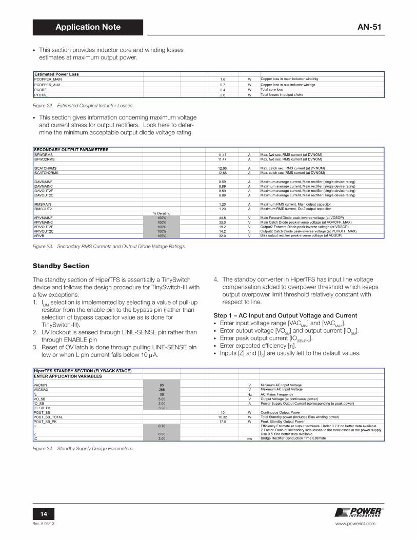
Figure 22. Estimated Coupled Inductor Losses.
Figure 24. Standby Supply Design Parameters.
• This section provides inductor core and winding losses estimates at maximum output power.
• This section gives information concerning maximum voltage and current stress for output rectifiers. Look here to deter-mine the minimum acceptable output diode voltage rating.
Standby Section
The standby section of HiperTFS is essentially a TinySwitch device and follows the design procedure for TinySwitch-III with a few exceptions:1. ILIM selection is implemented by selecting a value of pull-up
resistor from the enable pin to the bypass pin (rather than selection of bypass capacitor value as is done for TinySwitch-III).
2. UV lockout is sensed through LINE-SENSE pin rather than through ENABLE pin
3. Reset of OV latch is done through pulling LINE-SENSE pin low or when L pin current falls below 10 mA.
Figure 23. Secondary RMS Currents and Output Diode Voltage Ratings.
4. The standby converter in HiperTFS has input line voltage compensation added to overpower threshold which keeps output overpower limit threshold relatively constant with respect to line.
Step 1 – AC Input and Output Voltage and Current• Enter input voltage range [VACMIN] and [VACMAX].• Enter output voltage [VOSB] and output current [IOSB].• Enter peak output current [IO(SB)(PK)].• Enter expected efficiency [η].• Inputs [Z] and [tC] are usually left to the default values.
Estimated Power LossPCOPPER_MAIN 1.6 W Copper loss in main inductor windinig
PCOPPER_AUX 0.7 W Copper loss in aux inductor winidgs
PCORE 0.4 W Total core loss
PTOTAL 2.6 W Total losses in output choke
SECONDARY OUTPUT PARAMETERSISFWDRMS 11.47 A Max. fwd sec. RMS current (at DVNOM)ISFWD2RMS 11.47 A Max. fwd sec. RMS current (at DVNOM)
ISCATCHRMS 12.66 A Max. catch sec. RMS current (at DVNOM)ISCATCH2RMS 12.66 A Max. catch sec. RMS current (at DVNOM)
IDAVMAINF 8.59 A Maximum average current, Main rectifier (single device rating)IDAVMAINC 8.89 A Maximum average current, Main rectifier (single device rating)IDAVOUT2F 8.59 A Maximum average current, Main rectifier (single device rating)IDAVOUT2C 8.89 A Maximum average current, Main rectifier (single device rating)
IRMSMAIN 1.20 A Maximum RMS current, Main output capacitorIRMSOUT2 1.20 A Maximum RMS current, Out2 output capacitor
% DeratingVPIVMAINF 100% 44.8 V Main Forward Diode peak-inverse voltage (at VDSOP)VPIVMAINC 100% 33.0 V Main Catch Diode peak-inverse voltage (at VOVOFF_MAX)VPIVOUT2F 100% 19.2 V Output2 Forward Diode peak-inverse voltage (at VDSOP)VPIVOUT2C 100% 14.2 V Output2 Catch Diode peak-inverse voltage (at VOVOFF_MAX)VPIVB 100% 32.0 V Bias output rectifier peak-inverse voltage (at VDSOP)
HiperTFS STANDBY SECTION (FLYBACK STAGE)ENTER APPLICATION VARIABLES
VACMIN 85 V Minimum AC Input VoltageVACMAX 265 V Maximum AC Input Voltage
fL 50 Hz AC Mains FrequencyVO_SB 5.00 V Output Voltage (at continuous power)IO_SB 2.00 A Power Supply Output Current (corresponding to peak power)IO_SB_PK 3.50POUT_SB 10 W Continuous Output PowerPOUT_SB_TOTAL 10.32 W Total Standby power (Includes Bias winding power)POUT_SB_PK 17.5 W Peak Standby Output Powern 0.70 Efficiency Estimate at output terminals. Under 0.7 if no better data available
Z 0.50Z Factor. Ratio of secondary side losses to the total losses in the power supply. Use 0.5 if no better data available
tC 3.00 ms Bridge Rectifier Conduction Time Estimate
Rev. A 03/13
15
Application Note
www.powerint.com
AN-51
Figure 26. Standby Bias Winding Voltage and Input Undervoltage.
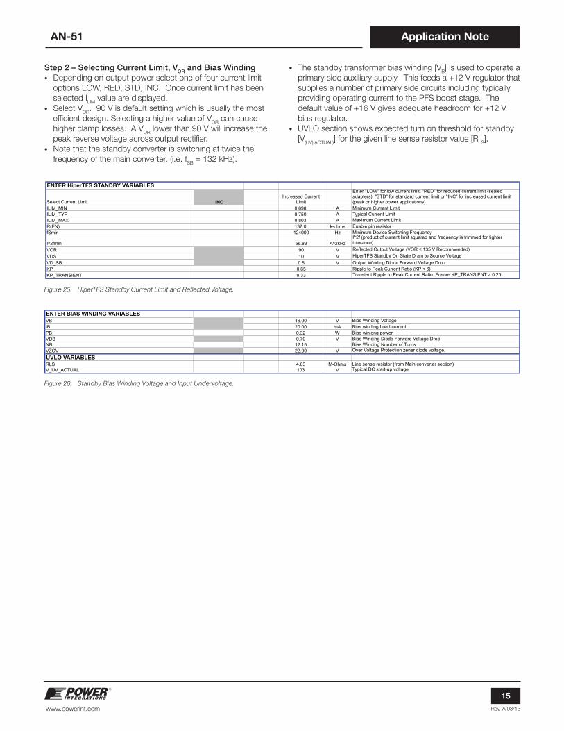
Figure 25. HiperTFS Standby Current Limit and Reflected Voltage.
Step 2 – Selecting Current Limit, VOR and Bias Winding• Depending on output power select one of four current limit
options LOW, RED, STD, INC. Once current limit has been selected ILIM value are displayed.
• Select VOR. 90 V is default setting which is usually the most efficient design. Selecting a higher value of VOR can cause higher clamp losses. A VOR lower than 90 V will increase the peak reverse voltage across output rectifier.
• Note that the standby converter is switching at twice the frequency of the main converter. (i.e. fSB = 132 kHz).
• The standby transformer bias winding [VB] is used to operate a primary side auxiliary supply. This feeds a +12 V regulator that supplies a number of primary side circuits including typically providing operating current to the PFS boost stage. The default value of +16 V gives adequate headroom for +12 V bias regulator.
• UVLO section shows expected turn on threshold for standby [V(UV)(ACTUAL)] for the given line sense resistor value [RLS].
ENTER HiperTFS STANDBY VARIABLES
Select Current Limit INCIncreased Current
Limit
Enter "LOW" for low current limit, "RED" for reduced current limit (sealed adapters), "STD" for standard current limit or "INC" for increased current limit (peak or higher power applications)
ILIM_MIN 0.698 A Minimum Current LimitILIM_TYP 0.750 A Typical Current LimitILIM_MAX 0.803 A Maximum Current LimitR(EN) 137.0 k-ohms Enable pin resistorfSmin 124000 Hz Minimum Device Switching Frequency
I^2fmin 66.83 A^2kHzI^2f (product of current limit squared and frequency is trimmed for tighter tolerance)
VOR 90 V Reflected Output Voltage (VOR < 135 V Recommended)
VDS 10 V HiperTFS Standby On State Drain to Source Voltage
VD_SB 0.5 V Output Winding Diode Forward Voltage DropKP 0.65 Ripple to Peak Current Ratio (KP < 6)KP_TRANSIENT 0.33 Transient Ripple to Peak Current Ratio. Ensure KP_TRANSIENT > 0.25
ENTER BIAS WINDING VARIABLESVB 16.00 V Bias Winding VoltageIB 20.00 mA Bias winding Load currentPB 0.32 W Bias winidng powerVDB 0.70 V Bias Winding Diode Forward Voltage DropNB 12.15 Bias Winding Number of TurnsVZOV 22.00 V Over Voltage Protection zener diode voltage.
UVLO VARIABLESRLS 4.03 M-Ohms Line sense resistor (from Main converter section)V_UV_ACTUAL 103 V Typical DC start-up voltage
Rev. A 03/13
16
Application Note
www.powerint.com
AN-51
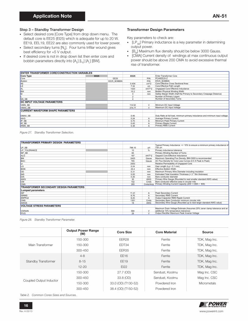
Step 3 – Standby Transformer Design• Select desired core [Core Type] from drop down menu. The
default core is EE25 (EI25) which is adequate for up to 20 W. EE19, EEL19, EE22 are also commonly used for lower power.
• Select secondary turns [NS]. Four turns trifilar wound gives best efficiency for +5 V output.
• If desired core is not in drop down list then enter core and bobbin parameters directly into [AE] [LE] [AL] [BW].
Figure 27. Standby Transformer Selection.
Figure 28. Standby Transformer Parameter.
Transformer Design Parameters
Key parameters to check are:• [LPSB] Primary inductance is a key parameter in determining
output power.• [BM] Maximum flux density should be below 3000 Gauss.• [CMA] Current density of windings at max continuous output
power should be above 200 CMA to avoid excessive thermal rise of transformer.
ENTER TRANSFORMER CORE/CONSTRUCTION VARIABLESCore Type EE25 EE25 Enter Transformer CoreCore EE25 P/N: PC40EE25-ZBobbin EE25_BOBBIN P/N: EE25_BOBBINAE 0.404 cm^2 Core Effective Cross Sectional AreaLE 7.34 cm Core Effective Path LengthAL 1420 nH/T^2 Ungapped Core Effective InductanceBW 10.2 mm Bobbin Physical Winding WidthM 0 mm Safety Margin Width (Half the Primary to Secondary Creepage Distance)L 2 Number of Primary LayersNS_SB 4 Number of Secondary Turns
DC INPUT VOLTAGE PARAMETERSVMIN_SB 114.52 V Minimum DC Input VoltageVMAX_SB 374.77 V Maximum DC Input Voltage
CURRENT WAVEFORM SHAPE PARAMETERS
DMAX_SB 0.46 Duty Ratio at full load, minimum primary inductance and minimum input voltageIAVG 0.24 A Average Primary CurrentIP_SB 0.70 A Minimum Peak Primary CurrentIR_SB 0.45 A Primary Ripple CurrentIRMS_SB 0.38 A Primary RMS Current
TRANSFORMER PRIMARY DESIGN PARAMETERS
LP_SB 799.10 uHTypical Primary Inductance. +/- 10% to ensure a minimum primary inductance of 726 uH
LP_TOLERANCE 10 % Primary inductance toleranceNP_SB 65 Primary Winding Number of TurnsALG 187 nH/T^2 Gapped Core Effective InductanceBM 2425 Gauss Maximum Operating Flux Density, BM<3000 is recommendedBAC 785 Gauss AC Flux Density for Core Loss Curves (0.5 X Peak to Peak)ur 2053 Relative Permeability of Ungapped CoreLG 0.24 mm Gap Length (Lg > 0.1 mm)BWE 20.4 mm Effective Bobbin WidthOD 0.31 mm Maximum Primary Wire Diameter including insulationINS 0.05 mm Estimated Total Insulation Thickness (= 2 * film thickness)DIA 0.26 mm Bare conductor diameterAWG 30 AWG Primary Wire Gauge (Rounded to next smaller standard AWG value)CM 102 Cmils Bare conductor effective area in circular milsCMA 265 Cmils/Amp Primary Winding Current Capacity (200 < CMA < 500)
TRANSFORMER SECONDARY DESIGN PARAMETERS Lumped parametersISP 11.41 A Peak Secondary CurrentISRMS 6.76 A Secondary RMS CurrentIRIPPLE 6.45 A Output Capacitor RMS Ripple CurrentCMS 1351 Cmils Secondary Bare Conductor minimum circular milsAWGS 18 AWG Secondary Wire Gauge (Rounded up to next larger standard AWG value)
VOLTAGE STRESS PARAMETERS
VDRAIN 584 VMaximum Drain Voltage Estimate (Assumes 20% zener clamp tolerance and an additional 10% temperature tolerance)
PIVS 28 V Output Rectifier Maximum Peak Inverse Voltage
Output Power Range(W) Core Size Core Material Source
Main Transformer
150-300 EER28 Ferrite TDK, Mag Inc.
150-300 EDT34 Ferrite TDK, Mag Inc.
300-450 EER35 Ferrite TDK, Mag Inc.
Standby Transformer
4-8 EE16 Ferrite TDK, Mag Inc.
8-15 EE19 Ferrite TDK, Mag Inc.
12-20 EI22 Ferrite TDK, Mag Inc.
Coupled Output Inductor
150-300 27.7 (OD) Sendust, Koolmu Mag Inc. CSC
300-450 33.8 (OD) Sendust, Koolmu Mag Inc. CSC
150-300 33.0 (OD) (T130-52) Powdered Iron Micrometals
300-450 38.4 (OD) (T150-52) Powdered Iron
Table 2. Common Cores Sizes and Sources.
Rev. A 03/13
17
Application Note
www.powerint.com
AN-51
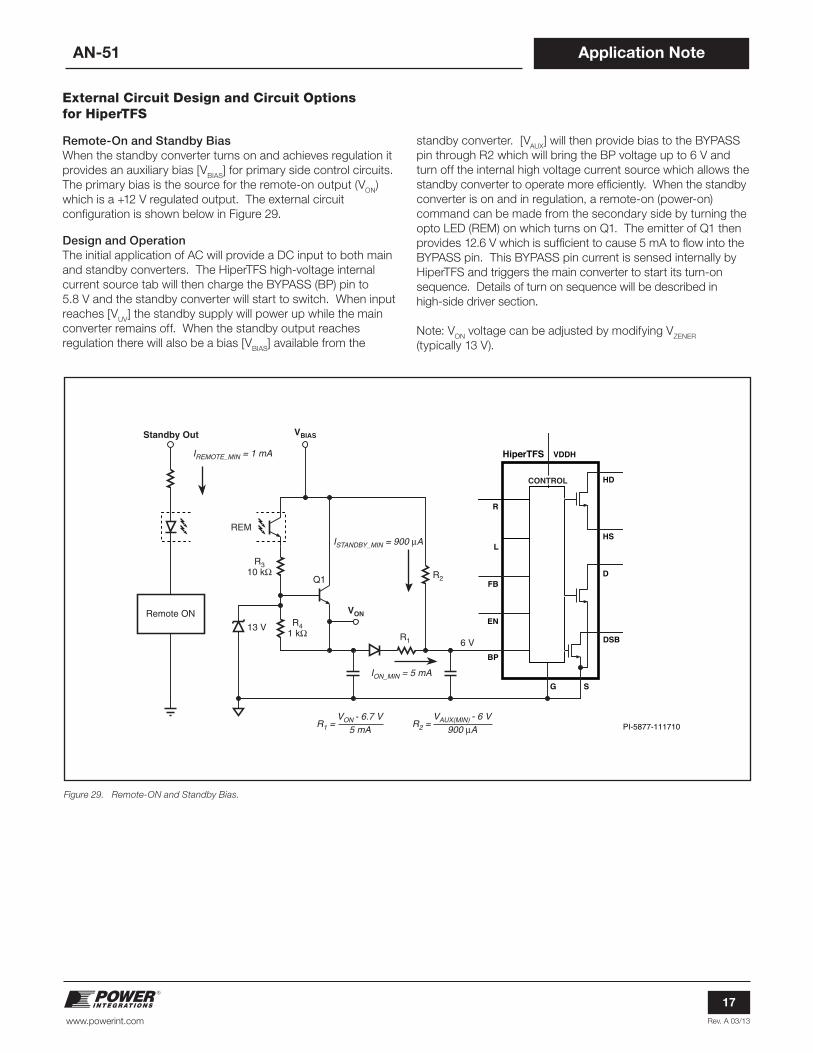
Figure 29. Remote-ON and Standby Bias.
External Circuit Design and Circuit Options for HiperTFS
Remote-On and Standby BiasWhen the standby converter turns on and achieves regulation it provides an auxiliary bias [VBIAS] for primary side control circuits. The primary bias is the source for the remote-on output (VON) which is a +12 V regulated output. The external circuit configuration is shown below in Figure 29.
Design and OperationThe initial application of AC will provide a DC input to both main and standby converters. The HiperTFS high-voltage internal current source tab will then charge the BYPASS (BP) pin to 5.8 V and the standby converter will start to switch. When input reaches [VUV] the standby supply will power up while the main converter remains off. When the standby output reaches regulation there will also be a bias [VBIAS] available from the
standby converter. [VAUX] will then provide bias to the BYPASS pin through R2 which will bring the BP voltage up to 6 V and turn off the internal high voltage current source which allows the standby converter to operate more efficiently. When the standby converter is on and in regulation, a remote-on (power-on) command can be made from the secondary side by turning the opto LED (REM) on which turns on Q1. The emitter of Q1 then provides 12.6 V which is sufficient to cause 5 mA to flow into the BYPASS pin. This BYPASS pin current is sensed internally by HiperTFS and triggers the main converter to start its turn-on sequence. Details of turn on sequence will be described in high-side driver section.
Note: VON voltage can be adjusted by modifying VZENER (typically 13 V).
HD
HS
D
G S
HiperTFS VDDH
R
L
FB
EN
BP
DSB
CONTROL
PI-5877-111710
Standby Out VBIAS
R310 kΩ
Q1
R41 kΩ13 V
REM
R1 6 V
R2
IREMOTE_MIN = 1 mA
ISTANDBY_MIN = 900 µA
ION_MIN = 5 mA
VON
R1 =VON - 6.7 V
5 mAR2 =
VAUX(MIN) - 6 V900 µA
Remote ON
Rev. A 03/13
18
Application Note
www.powerint.com
AN-51
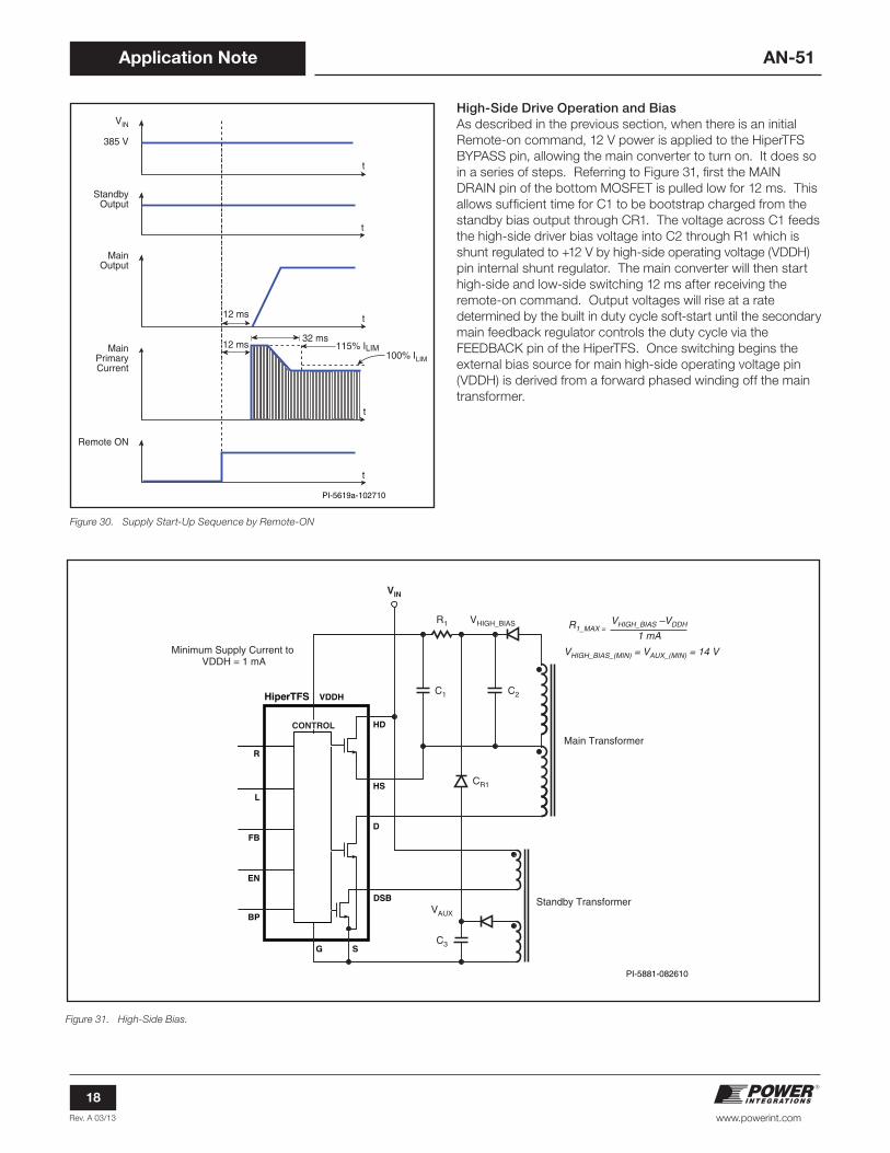
High-Side Drive Operation and BiasAs described in the previous section, when there is an initial Remote-on command, 12 V power is applied to the HiperTFS BYPASS pin, allowing the main converter to turn on. It does so in a series of steps. Referring to Figure 31, first the MAIN DRAIN pin of the bottom MOSFET is pulled low for 12 ms. This allows sufficient time for C1 to be bootstrap charged from the standby bias output through CR1. The voltage across C1 feeds the high-side driver bias voltage into C2 through R1 which is shunt regulated to +12 V by high-side operating voltage (VDDH) pin internal shunt regulator. The main converter will then start high-side and low-side switching 12 ms after receiving the remote-on command. Output voltages will rise at a rate determined by the built in duty cycle soft-start until the secondary main feedback regulator controls the duty cycle via the FEEDBACK pin of the HiperTFS. Once switching begins the external bias source for main high-side operating voltage pin (VDDH) is derived from a forward phased winding off the main transformer.
Figure 31. High-Side Bias.
Figure 30. Supply Start-Up Sequence by Remote-ON
VIN
StandbyOutput
MainOutput
12 ms
385 V
MainPrimaryCurrent
Remote ON
12 ms32 ms
t
t
t
t
t
PI-5619a-102710
100% ILIM
115% ILIM
HD
HS
D
G S
HiperTFS VDDH
R
L
FB
EN
BP
DSB
CONTROL
PI-5881-082610
C3
C1
R1
VIN
VAUX
C2
CR1
Minimum Supply Current to VDDH = 1 mA
Main Transformer
VHIGH_BIAS
Standby Transformer
VHIGH_BIAS_(MIN) = VAUX_(MIN) = 14 V
VHIGH_BIAS –VDDH
1 mAR1_MAX =
Rev. A 03/13
19
Application Note
www.powerint.com
AN-51
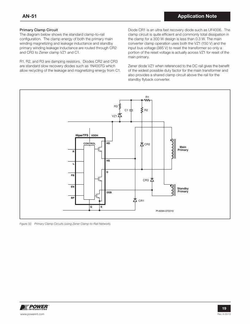
Figure 32. Primary Clamp Circuits (using Zener Clamp-to-Rail Network).
Primary Clamp CircuitThe diagram below shows the standard clamp-to-rail configuration. The clamp energy of both the primary main winding magnetizing and leakage inductance and standby primary winding leakage inductance are routed through CR2 and CR3 to Zener clamp VZ1 and C1.
R1, R2, and R3 are damping resistors. Diodes CR2 and CR3 are standard slow recovery diodes such as 1N4007G which allow recycling of the leakage and magnetizing energy from C1.
Diode CR1 is an ultra fast recovery diode such as UF4006. The clamp circuit is quite efficient and commonly total dissipation in the clamp for a 300 W design is less than 0.3 W. The main converter clamp operation uses both the VZ1 (150 V) and the input bus voltage (385 V) to reset the transformer so only a portion of the reset voltage is actually across VZ1 for reset of the main primary.
Zener diode VZ1 when referenced to the DC rail gives the benefit of the widest possible duty factor for the main transformer and also provides a shared clamp circuit above the rail for the standby flyback converter.
HD
HS
D
G S
HiperTFS VDDH
R
L
FB
EN
BP
DSB
CONTROL
PI-6094-072210
R1
R2C1
CR2
CR3
CR1
R3
VZ1
StandbyPrimary
MainPrimary
Rev. A 03/13
20
Application Note
www.powerint.com
AN-51
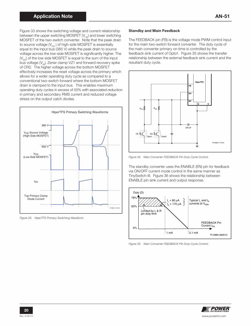
Figure 33 shows the switching voltage and current relationship between the upper switching MOSFET (VHS) and lower switching MOSFET of the two-switch converter. Note that the peak drain to source voltage (VDS ) of high-side MOSFET is essentially equal to the input bus (385 V) while the peak drain to source voltage across the low-side MOSFET is significantly higher. The (VDS) of the low-side MOSFET is equal to the sum of the input bus voltage (VIN), Zener clamp VZ1 and forward recovery spike of CR2. The higher voltage across the bottom MOSFET effectively increases the reset voltage across the primary which allows for a wider operating duty cycle as compared to a conventional two-switch forward where the bottom MOSFET drain is clamped to the input bus. This enables maximum operating duty cycles in excess of 50% with associated reduction in primary and secondary RMS current and reduced voltage stress on the output catch diodes.
Figure 33. HiperTFS Primary Switching Waveform.
Figure 35. Main Converter FEEDBACK Pin Duty Cycle Control.
Figure 34. Main Converter FEEDBACK Pin Duty Cycle Control.
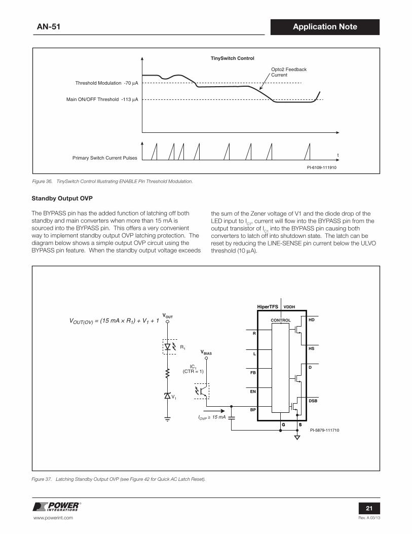
Standby and Main Feedback
The FEEDBACK pin (FB) is the voltage mode PWM control input for the main two-switch forward converter. The duty cycle of the main converter primary on-time is controlled by the feedback sink current of Opto1. Figure 35 shows the transfer relationship between the external feedback sink current and the resultant duty cycle.
The standby converter uses the ENABLE (EN) pin for feedback via ON/OFF current mode control in the same manner as TinySwitch-III. Figure 36 shows the relationship between ENABLE pin sink current and output response.
PI-5616-111910
VHS Source Voltage(High-Side MOSFET)
VDS(Low-Side MOSFET)
IDS
Top Primary ClampDiode Current
HiperTFS Primary Switching Waveforms
385 V
560 V
63%
78%
0%
1 mA 2.1 mA
Duty (D)
FEEDBACK PinCurrent IFB
IL = 60 µAIR = 170 µA
Typical IL and IRcurrents at VMIN
Limited by L & Rpin duty limit
PI-5885-082610
G S
FB
EN
BP
PI-6093-111910
HiperTFS
RENRFB
Opto2
220 pF
FB ENOpto1
Rev. A 03/13
21
Application Note
www.powerint.com
AN-51
Figure 36. TinySwitch Control Illustrating ENABLE Pin Threshold Modulation.
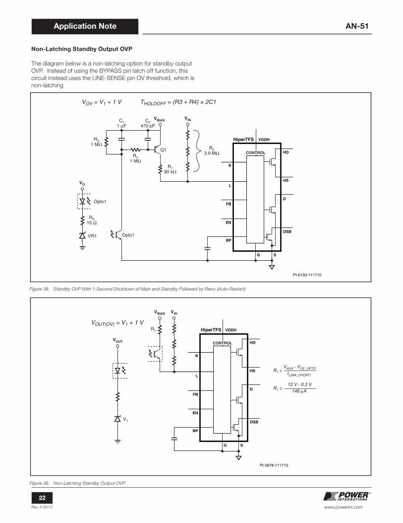
Standby Output OVP
The BYPASS pin has the added function of latching off both standby and main converters when more than 15 mA is sourced into the BYPASS pin. This offers a very convenient way to implement standby output OVP latching protection. The diagram below shows a simple output OVP circuit using the BYPASS pin feature. When the standby output voltage exceeds
Figure 37. Latching Standby Output OVP (see Figure 42 for Quick AC Latch Reset).
the sum of the Zener voltage of V1 and the diode drop of the LED input to IC1, current will flow into the BYPASS pin from the output transistor of IC1 into the BYPASS pin causing both converters to latch off into shutdown state. The latch can be reset by reducing the LINE-SENSE pin current below the ULVO threshold (10 mA).
PI-6109-111910
TinySwitch Control
Opto2 FeedbackCurrent
t
Threshold Modulation -70 µA
Main ON/OFF Threshold -113 µA
Primary Switch Current Pulses
HD
HS
D
G S
HiperTFS VDDH
R
L
FB
EN
BP
DSB
CONTROL
PI-5879-111710G S
VBIAS
VOUT
R1
IC1(CTR = 1)
V1
VOUT(OV) = (15 mA × R1) + V1 + 1
IOVP ≥ 15 mA
Rev. A 03/13
22
Application Note
www.powerint.com
AN-51
Figure 39. Non-Latching Standby Output OVP.
Figure 38. Standby OVP With 1-Second Shutdown of Main and Standby Followed by Retry (Auto-Restart)
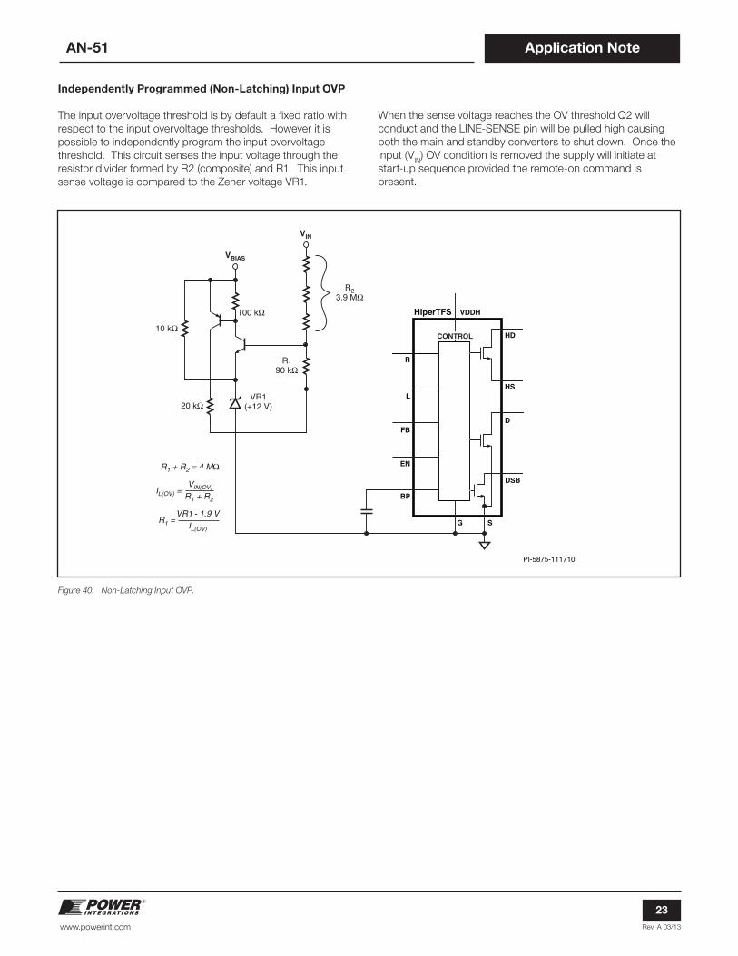
Non-Latching Standby Output OVP
The diagram below is a non-latching option for standby output OVP. Instead of using the BYPASS pin latch off function, this circuit instead uses the LINE-SENSE pin OV threshold, which is non-latching
HD
HS
D
G S
HiperTFS VDDH
R
L
FB
EN
BP
DSB
CONTROL
PI-5878-111710
VOUT
V1
VOUT(OV) = V1 + 1 V
VINVBIAS
R1 ≤
R1
VAUX - VCE_OPTO
IL(MA_OVOFF)
R1 ≤ 12 V - 0.3 V
146 µA
HD
HS
D
G S
HiperTFS VDDH
R
L
FB
EN
BP
DSB
CONTROL
PI-6133-111710
VBIAS
R31 MΩ
R190 kΩ
R510 Ω
Opto1
R41 MΩ
C11 µF
C2470 pF
VR1
VIN
VO
R23.9 MΩ
Q1
Opto1
VOV = V1 + 1 V THOLDOFF = (R3 + R4) × 2C1
Rev. A 03/13
23
Application Note
www.powerint.com
AN-51
Figure 40. Non-Latching Input OVP.
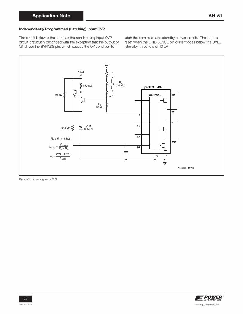
Independently Programmed (Non-Latching) Input OVP
The input overvoltage threshold is by default a fixed ratio with respect to the input overvoltage thresholds. However it is possible to independently program the input overvoltage threshold. This circuit senses the input voltage through the resistor divider formed by R2 (composite) and R1. This input sense voltage is compared to the Zener voltage VR1.
When the sense voltage reaches the OV threshold Q2 will conduct and the LINE-SENSE pin will be pulled high causing both the main and standby converters to shut down. Once the input (VIN) OV condition is removed the supply will initiate at start-up sequence provided the remote-on command is present.
HD
HS
D
G S
HiperTFS VDDH
R
L
FB
EN
BP
DSB
CONTROL
PI-5875-111710
VBIAS
20 kΩ
100 kΩ
10 kΩ
R190 kΩ
VR1(+12 V)
VIN
R23.9 MΩ
R1 + R2 = 4 MΩ
IL(OV) = VIN(OV)
R1 + R2
R1 =VR1 - 1.9 V
IL(OV)
Rev. A 03/13
24
Application Note
www.powerint.com
AN-51
Independently Programmed (Latching) Input OVP
The circuit below is the same as the non-latching input OVP circuit previously described with the exception that the output of Q1 drives the BYPASS pin, which causes the OV condition to
Figure 41. Latching Input OVP.
latch the both main and standby converters off. The latch is reset when the LINE-SENSE pin current goes below the UVLO (standby) threshold of 10 mA.
HD
HS
D
G S
HiperTFS VDDH
R
L
FB
EN
BP
DSB
CONTROL
PI-5876-111710
VIN
VBIAS
R190 kΩ
VR1(+12 V)300 kΩ
10 kΩ
R23.9 MΩ
R1 + R2 = 4 MΩ
IL(OV) = VIN(OV)
R1 + R2
R1 =VR1 - 1.9 V
IL(OV)
100 kΩ
Q1
Rev. A 03/13
25
Application Note
www.powerint.com
AN-51
Figure 42. Quick AC Reset of BP Latch (see Figure 37 BYPASS Pin Latch).
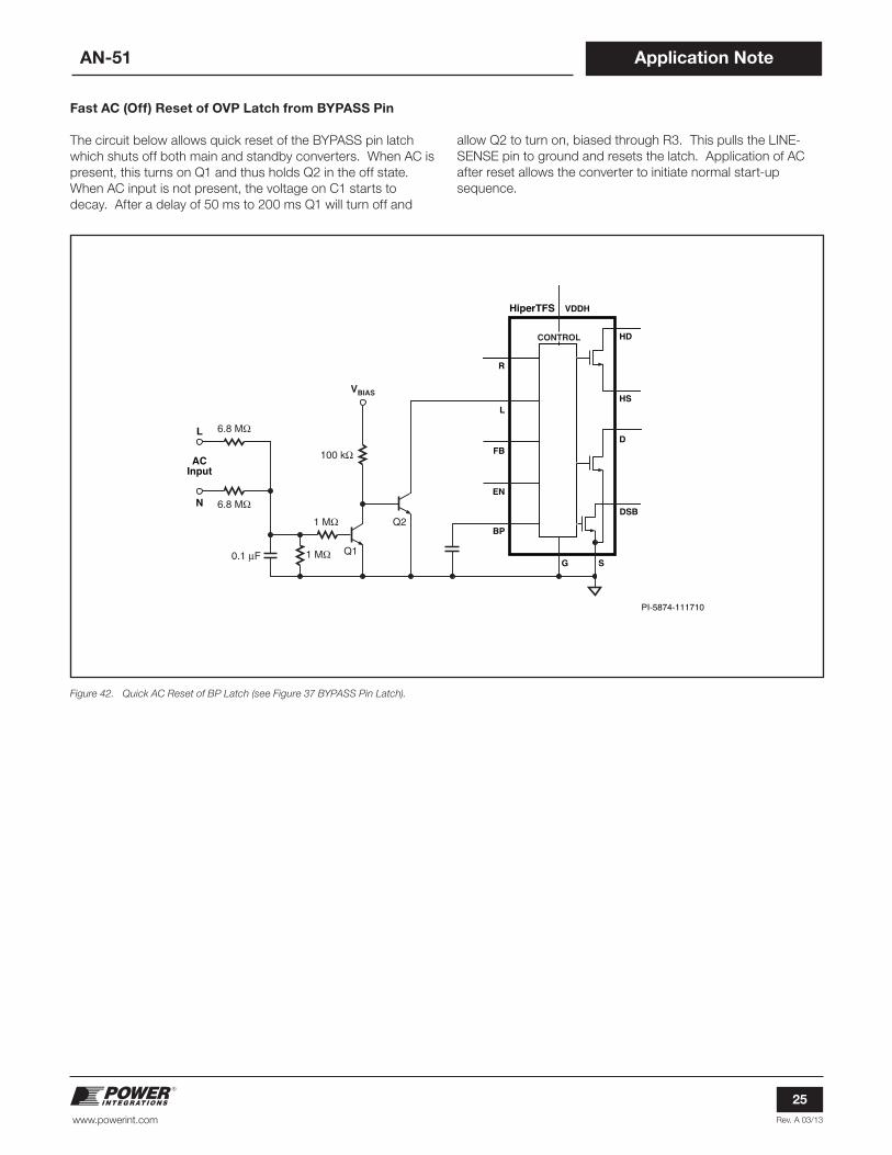
Fast AC (Off) Reset of OVP Latch from BYPASS Pin
The circuit below allows quick reset of the BYPASS pin latch which shuts off both main and standby converters. When AC is present, this turns on Q1 and thus holds Q2 in the off state. When AC input is not present, the voltage on C1 starts to decay. After a delay of 50 ms to 200 ms Q1 will turn off and
allow Q2 to turn on, biased through R3. This pulls the LINE-SENSE pin to ground and resets the latch. Application of AC after reset allows the converter to initiate normal start-up sequence.
HD
HS
ACInput
D
G S
HiperTFS VDDH
L
N
R
L
FB
EN
BP
DSB
CONTROL
PI-5874-111710
100 kΩ
Q1
Q2
0.1 µF
1 MΩ
6.8 MΩ
VBIAS
6.8 MΩ
1 MΩ
Rev. A 03/13
26
Application Note
www.powerint.com
AN-51
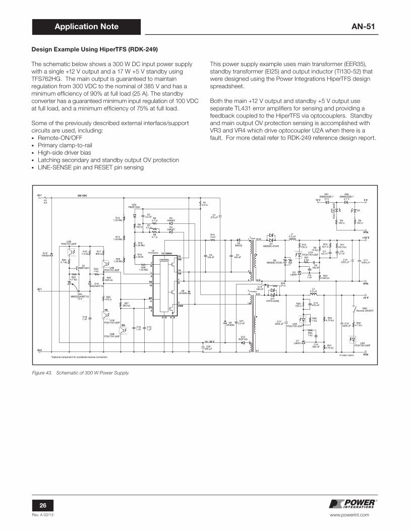
Design Example Using HiperTFS (RDK-249)
The schematic below shows a 300 W DC input power supply with a single +12 V output and a 17 W +5 V standby using TFS762HG. The main output is guaranteed to maintain regulation from 300 VDC to the nominal of 385 V and has a minimum efficiency of 90% at full load (25 A). The standby converter has a guaranteed minimum input regulation of 100 VDC at full load, and a minimum efficiency of 75% at full load.
Some of the previously described external interface/support circuits are used, including:• Remote-ON/OFF• Primary clamp-to-rail • High-side driver bias• Latching secondary and standby output OV protection• LINE-SENSE pin and RESET pin sensing
This power supply example uses main transformer (EER35), standby transformer (EI25) and output inductor (TI130-52) that were designed using the Power Integrations HiperTFS design spreadsheet.
Both the main +12 V output and standby +5 V output use separate TL431 error amplifiers for sensing and providing a feedback coupled to the HiperTFS via optocouplers. Standby and main output OV protection sensing is accomplished with VR3 and VR4 which drive optocoupler U2A when there is a fault. For more detail refer to RDK-249 reference design report.
Figure 43. Schematic of 300 W Power Supply.
HD
14 - 25 V
D5BAV20
VR4MMSZ5243BT1G
13 V
D7M6060C-E3/45
D6M6060C-E3/45
D9UF4005
C212.2 nF
L13.3 µH
C4100 nF
C547 nF
C103300 µF
C113300 µF
R212 kΩ
R28100 Ω
R301 kΩ
R344.75 kΩ
R314.75 kΩ
U7LM431
U5LM431
R331 kΩ
R324.7 kΩ
SW1Remote ON/OFF
U3APC817XI1J00F
R243.92 kΩ
R3100 Ω
R4150 Ω
RTN
5 V12 V
D2
U4A
PC81
7XI1
JD0F
VR1ZMM5242B-7
12 V
VR2ZMM5230B-7
4.7 V
R15750 Ω
U1APC817XI1J00F
R915 kΩ
R10221 Ω
C91 nF
D8UF4005
C191 nF
C20330 µF
*Optional component for accidental reverse connection
R2647 Ω
C172200 µF U2A
PC817XI1J00F
C14470 nF
C16330 nF
C152200 µF
C13100 nF
U2BPC817XI1J00F
U1BPC817XI1J00F
R25232 kΩ
R27280 kΩ
D10BAS16HT1G
J3-1
J4-1
J3-3
R14 2 kΩ
C6100 nF
C3100 nF
D31N4007
R54.7 Ω
R12.2 Ω
C1270 µF
F24 A
D13*1N5404
R204.7 kΩ
R167.5 kΩ
R17820 Ω
R351.33 MΩ
R131.33 MΩ
R121.33 MΩ
R231 kΩ
R224.7 kΩ
U3BPC817X1J00F
U4BPC817X1J00F
R6100 Ω
VR3P6KE150A
R181.33 MΩ
R191.33 M
R361.33 MΩ
R84.7 Ω
U6TFS762HG
D41N4007
D12RGP100
D11STPS1045B
3
5
2
1
2
6
9,10
9,10
13,14
1
HS
380 VDC
RTN
RTN
FB
EN
TSTANDBY
TMAIN
D
G S5 6
VDDH13
R
L
FB
BP
EN
7
9
10
11
8
DSB
16
14
1
3
PI-5969-102810
C121 µF
6,7
CONTROL
+12 V
+5 VR29470 Ω
L22.2 µH
R74.7 Ω
C181 nF
C23.3 nF
C8100 nF
R1143.2 kΩ
Q1MMBT4401
Rev. A 03/13
27
Application Note
www.powerint.com
AN-51
Figure 44. Layout of High-Efficiency +12 V, 25 A Main Output and +5 V, 2.5 A Standby Power Supply.
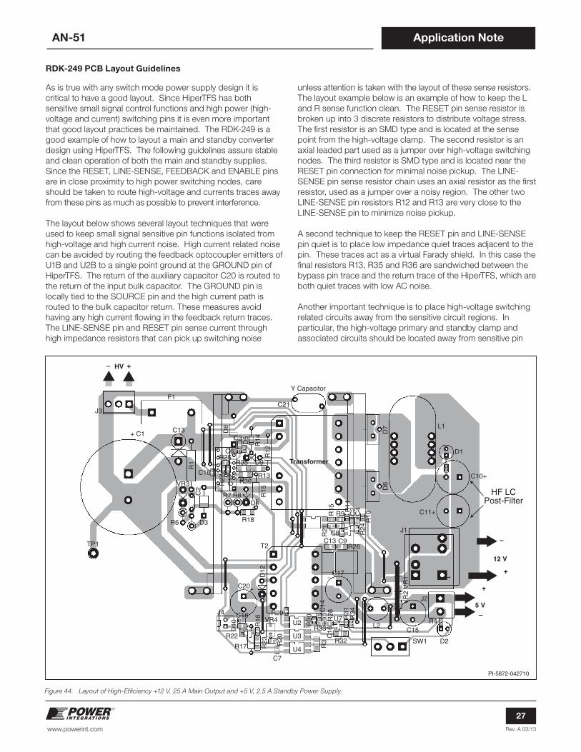
RDK-249 PCB Layout Guidelines
As is true with any switch mode power supply design it is critical to have a good layout. Since HiperTFS has both sensitive small signal control functions and high power (high- voltage and current) switching pins it is even more important that good layout practices be maintained. The RDK-249 is a good example of how to layout a main and standby converter design using HiperTFS. The following guidelines assure stable and clean operation of both the main and standby supplies. Since the RESET, LINE-SENSE, FEEDBACK and ENABLE pins are in close proximity to high power switching nodes, care should be taken to route high-voltage and currents traces away from these pins as much as possible to prevent interference.
The layout below shows several layout techniques that were used to keep small signal sensitive pin functions isolated from high-voltage and high current noise. High current related noise can be avoided by routing the feedback optocoupler emitters of U1B and U2B to a single point ground at the GROUND pin of HiperTFS. The return of the auxiliary capacitor C20 is routed to the return of the input bulk capacitor. The GROUND pin is locally tied to the SOURCE pin and the high current path is routed to the bulk capacitor return. These measures avoid having any high current flowing in the feedback return traces. The LINE-SENSE pin and RESET pin sense current through high impedance resistors that can pick up switching noise
unless attention is taken with the layout of these sense resistors. The layout example below is an example of how to keep the L and R sense function clean. The RESET pin sense resistor is broken up into 3 discrete resistors to distribute voltage stress. The first resistor is an SMD type and is located at the sense point from the high-voltage clamp. The second resistor is an axial leaded part used as a jumper over high-voltage switching nodes. The third resistor is SMD type and is located near the RESET pin connection for minimal noise pickup. The LINE-SENSE pin sense resistor chain uses an axial resistor as the first resistor, used as a jumper over a noisy region. The other two LINE-SENSE pin resistors R12 and R13 are very close to the LINE-SENSE pin to minimize noise pickup.
A second technique to keep the RESET pin and LINE-SENSE pin quiet is to place low impedance quiet traces adjacent to the pin. These traces act as a virtual Farady shield. In this case the final resistors R13, R35 and R36 are sandwiched between the bypass pin trace and the return trace of the HiperTFS, which are both quiet traces with low AC noise.
Another important technique is to place high-voltage switching related circuits away from the sensitive circuit regions. In particular, the high-voltage primary and standby clamp and associated circuits should be located away from sensitive pin
+Ð HV
PI-5872-042710
Transformer
L1
D1
D7
VR
1V
R2
D6
C10+
D2SW1
R4L2
R26
R29VR4
R17
R22
C18
C20
J4
C7
C17
T2
U4
U2U7
U3R32
R33
C13C8
C9
R11
C2
R10C
4R
24
R21
R15
D8
R12
R1
C2
D5
R14
R15
C12
R27
R34
R20
R16
D12
D10
R23
C16
R3
R31
R28
C14
R30
C15
C21F1
J3
+ C1
C16
C3C13
VR3
D3
TP1
R6
C11+
J1
R9
J2
R13
R18
R36
D4R7 R8
R35 D9
C6R25
Y Capacitor
HF LCPost-Filter
5 V
+
Ð
12 V
+
Ð

Rev. A 03/13
28
Application Note
www.powerint.com
AN-51
circuits. The boot-strap diode D9 is close to the high-side operating voltage pin to minimize the length of the cathode trace, which has high-voltage switching. Finally, the main transformer is close to the HiperTFS device to keep high voltage switching traces short.
Retrofit 300 W PC Main and PC Standby Using HiperPFS and HiperTFS Meeting 80 PLUS Bronze Efficiency
The design in Figure 46 is an example of a complete 300 W PC power supply with power factor corrected front end using
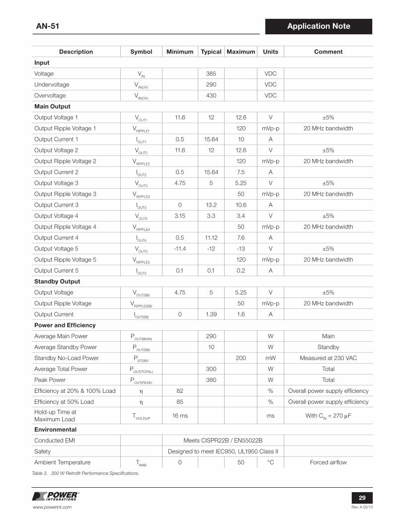
HiperPFS providing 385 VDC to a DC-DC converter stage using HiperTFS. The design was built by removing the primary side circuitry of an existing ATX power supply and grafting on a new primary section incorporating the HiperTFS and HiperPFC converter circuits. The layout for the primary side is included below. The secondary schematic (Figure 47) shows the power and feedback circuits of original design. The original enclosure, output diodes, fan and heat sinks were used. The output choke was designed using HiperTFS spreadsheet. The table below shows performance specifications that this design meets.
Rev. A 03/13
29
Application Note
www.powerint.com
AN-51
Table 3. 300 W Retrofit Performance Specifications.
Description Symbol Minimum Typical Maximum Units Comment
Input
Voltage VIN 385 VDC
Undervoltage VIN(UV) 290 VDC
Overvoltage VIN(OV) 430 VDC
Main Output
Output Voltage 1 VOUT1 11.6 12 12.6 V ±5%
Output Ripple Voltage 1 VRIPPLE1 120 mVp-p 20 MHz bandwidth
Output Current 1 IOUT1 0.5 15.64 10 A
Output Voltage 2 VOUT2 11.6 12 12.6 V ±5%
Output Ripple Voltage 2 VRIPPLE2 120 mVp-p 20 MHz bandwidth
Output Current 2 IOUT2 0.5 15.64 7.5 A
Output Voltage 3 VOUT3 4.75 5 5.25 V ±5%
Output Ripple Voltage 3 VRIPPLE3 50 mVp-p 20 MHz bandwidth
Output Current 3 IOUT3 0 13.2 10.6 A
Output Voltage 4 VOUT4 3.15 3.3 3.4 V ±5%
Output Ripple Voltage 4 VRIPPLE4 50 mVp-p 20 MHz bandwidth
Output Current 4 IOUT4 0.5 11.12 7.6 A
Output Voltage 5 VOUT5 -11.4 -12 -13 V ±5%
Output Ripple Voltage 5 VRIPPLE5 120 mVp-p 20 MHz bandwidth
Output Current 5 IOUT5 0.1 0.1 0.2 A
Standby Output
Output Voltage VOUT(SB) 4.75 5 5.25 V ±5%
Output Ripple Voltage VRIPPLE(SB) 50 mVp-p 20 MHz bandwidth
Output Current IOUT(SB) 0 1.39 1.6 A
Power and Efficiency
Average Main Power POUT(MAIN) 290 W Main
Average Standby Power POUT(SB) 10 W Standby
Standby No-Load Power PSTDBY 200 mW Measured at 230 VAC
Average Total Power POUT(TOTAL) 300 W Total
Peak Power POUT(PEAK) 380 W Total
Efficiency at 20% & 100% Load η 82 % Overall power supply efficiency
Efficiency at 50% Load η 85 % Overall power supply efficiency
Hold-up Time at Maximum Load
THOLDUP 16 ms ms With CIN = 270 mF
Environmental
Conducted EMI Meets CISPR22B / EN55022B
Safety Designed to meet IEC950, UL1950 Class II
Ambient Temperature TAMB 0 50 °C Forced airflow
Rev. A 03/13
30
Application Note
www.powerint.com
AN-51
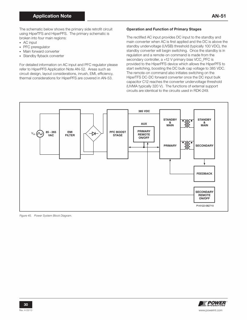
The schematic below shows the primary side retrofit circuit using HiperTFS and HiperPFS. The primary schematic is broken into four main regions:• AC input• PFC preregulator• Main forward converter• Standby flyback converter
For detailed information on AC input and PFC regulator please refer to HiperPFS Application Note AN-52. Areas such as circuit design, layout considerations, inrush, EMI, efficiency, thermal considerations for HiperPFS are covered in AN-53.
Operation and Function of Primary Stages
The rectified AC input provides DC input to the standby and main converter when AC is first applied and the DC is above the standby undervoltage (UVSB) threshold (typically 100 VDC), the standby converter will begin switching. Once the standby is in regulation and a remote-on command is made from the secondary controller, a +12 V primary bias VCC_PFC is provided to the HiperPFS device which allows the HiperPFS to start switching, boosting the DC bulk cap voltage to 385 VDC. The remote-on command also initiates switching on the HiperTFS DC-DC forward converter once the DC input bulk capacitor C12 reaches the converter undervoltage threshold (UVMA typically 320 V). The functions of external support circuits are identical to the circuits used in RDK-249.
Figure 45. Power System Block Diagram.
STANDBY&
MAIN
SECONDARY
PI-6122-082710
FEEDBACK
SECONDARYREMOTEON/OFF
PRIMARYREMOTEON/OFF
AUX
385 VDC
STANDBY&
MAIN
PRIMARY
VIN85 - 265
VACPFC BOOST
STAGEEMI
FILTER
Rev. A 03/13
31
Application Note
www.powerint.com
AN-51
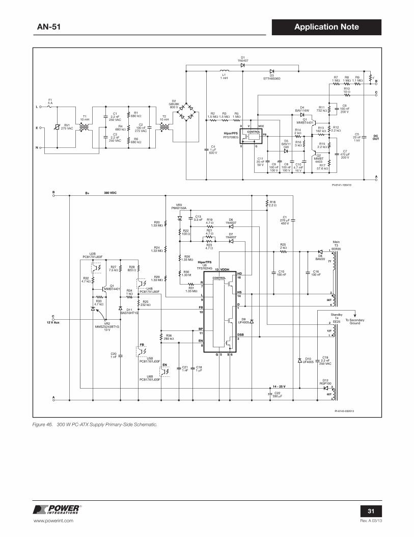
Figure 46. 300 W PC-ATX Supply Primary-Side Schematic.
HD
14 - 25 V
D8BAV20
VR2MMSZ5243BT1G
13 V
D10UF4005
C192.2 nF
250 VAC
To SecondaryGround
D9UF4005
C211 nF
C22330 µF
U6BPC817XI1J00F
U5BPC817XI1J00F
R25232 kΩ
R36280 kΩ
D11BAS16HT1G
B B+
C
12 V Aux
A
R25 2 kΩ
C15100 nF
C16100 nF
D61N4007
R194.7 Ω
R182.2 Ω
C1270 µF450 V
R324.7 kΩ
R277.5 kΩ
R28820 Ω
R291.33 MΩ
R241.33 MΩ
R201.33 MΩ
R341 kΩ
R334.7 kΩ
U2BPC817X1J00F
U4BPC817X1J00F
R22100 Ω
VR3P6KE150A
R261.33 MΩ
R301.33 M
R311.33 MΩ
R234.7 Ω
HiperTFSU6
TFS762HG
D71N4007
D12RGP100
3
5
2
1
7T
88T
12T
65T
2
6
1
HS
380 VDC
FB
EN
StandbyT4
EE25
MainT3
EER35
D
G S5 6
VDDH13
R
L
FB
BP
EN
7
9
10
11
8
DSB
16
14
1
3
C181 µF
CONTROL
R214.7 Ω
C201 nF
C133.3 nF
Q1MMBT4401
PI-6140-032013
PI-6141-100410
N
E
L
R1680 kΩ
R4680 kΩ
R6680 kΩ
R21.5 MΩ
R31.5 MΩ
R51 MΩT2
10 mH
L11 mH
D2GBU8K800 V
D11N5407
D4BAV116W
D5BAV11
GW
D3STTH8S06D
T110 mH
C2100 nF
275 VACC3
2.2 nF250 VAC
C41 µF
630 V
R11732 kΩ
R152.2 kΩ
R1757.6 kΩ
Q2MMBT4403
R142 kΩ
R163 kΩ
R122.2 kΩ
R1010 Ω
R71 MΩ
R81 MΩ
R91.1 MΩ
R13162 kΩ
C7470 pF200 V
C6100 nF200 V
C520 nF1 kV
C12.2 nF
250 VAC
F15 A
RV1275 VAC
D
S
FB
VCCV
G
DCOUT
CONTROL
B
A
C
HiperPFSPFS708EG
tO
C1120 nF50 V C9
100 nF100 V
C8100 nF100 V
C104.7 mF16 V
Q1MMBT4401
Rev. A 03/13
32
Application Note
www.powerint.com
AN-51
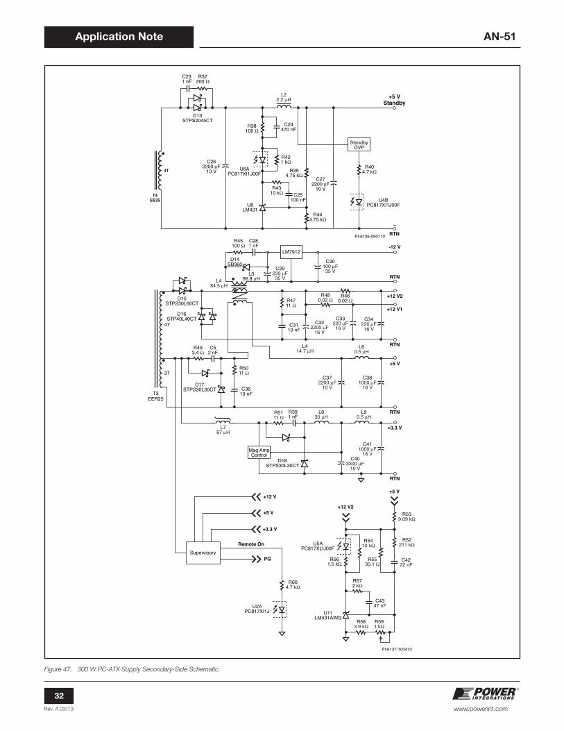
Figure 47. 300 W PC-ATX Supply Secondary-Side Schematic.
D15STPS30L60CT
D16STP40L40CT C33
220 µF16 V
C322200 µF
16 V
C30100 µF35 VC29
220 µF35 V
C281 nF
D14SB360
R45100 Ω
C34220 µF16 V
C3110 nF
R4711 Ω
RTN
RTN
-12 V
+12 V1
4T
3T
T3EER25
PI-6137-100410
+12 V2
C381000 µF
16 V
C372200 µF
10 V
C403300 µF
10 V
R583.9 kΩ
R591 kΩ
R572 kΩ
U11LM431AIM3
U2APC817XI1J
U5APC817XLIJ00F
R561.5 kΩ
R604.7 kΩ
R52211 kΩ
R539.09 kΩ
R5530.1 Ω
C4347 nF
C4222 nF
C411000 µF
16 V
C3610 nF
D17STPS30L30CT
D18STPS30L30CT
R5011 Ω
R493.4 Ω
R5111 Ω
R480.02 Ω
R460.02 Ω
RTN
+3.3 V
+12 V
+12 V2
+5 V
+5 V
+3.3 V
Remote On
RTN
PG
+5 V
R38100 Ω
R421 kΩ
R394.75 kΩ
R444.75 kΩ
U8LM431
R4310 kΩ
R404.7 kΩ
U4BPC817XI1J00F
R37200 Ω
C262200 µF
10 V U6APC817XI1J00F
C24470 nF
C25100 nF
C272200 µF
10 V
C231 nF
D13STPS2045CT
T4EE25
4T
RTN
+5 VStandby
L22.2 µH
PI-6126-090110
StandbyOVP
LM7912
Supervisory
Mag AmpControl
L396.8 µHL4
84.5 µH
L60.5 µH
L414.7 µH
C52 nF
L767 µH
L830 µH
L90.5 µH
R391 nF
R5410 kΩ
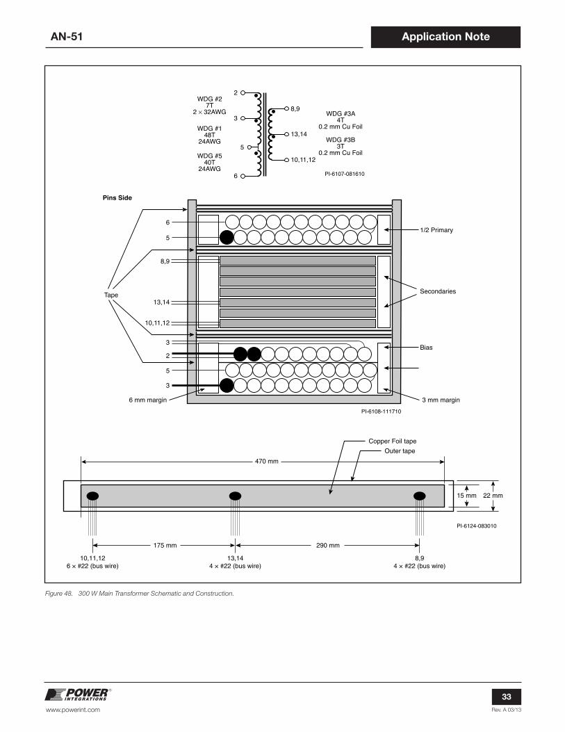
Rev. A 03/13
33
Application Note
www.powerint.com
AN-51
Figure 48. 300 W Main Transformer Schematic and Construction.
PI-6108-111710
Secondaries
Bias
Tape
3 mm margin
Pins Side
6 mm margin
8,9
5
6
13,14
10,11,12
3
5
2
3
1/2 Primary
WDG #27T
2 × 32AWG WDG #3A4T
0.2 mm Cu Foil
WDG #3B3T
0.2 mm Cu Foil
WDG #148T
24AWG
WDG #540T
24AWG
3
5
6
8,9
13,14
10,11,12
PI-6107-081610
2
PI-6124-083010
470 mm
15 mm 22 mm
175 mm 290 mm
Copper Foil tape
Outer tape
10,11,126 × #22 (bus wire)
13,144 × #22 (bus wire)
8,94 × #22 (bus wire)
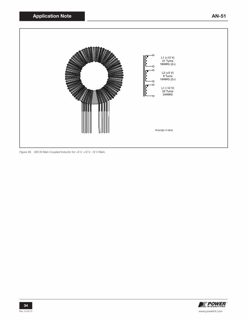
Rev. A 03/13
34
Application Note
www.powerint.com
AN-51
Figure 49. 300 W Main Coupled Inductor for +5 V, +12 V, -12 V Main.
L1 (+12 V)21 Turns
18AWG (2×)
L2 (+5 V)9 Turns
19AWG (2×)
L1 (-12 V)22 Turns24AWG
PI-6132-111810
Rev. A 03/13
35
Application Note
www.powerint.com
AN-51
Layout Considerations
For any switching power supply, layout is a critical aspect of a good design. Layout can effect stability, thermal rise of power components, EMI, and safety compliance. The key areas to consider for stable clean operation using HiperTFS have already been discussed in the RDK-249 section of the Application Note.
The key physical regions of the layout for this supply are:• AC input bridge• HiperPFS and boost diode heat sink• HiperTFS heat sink• Main transformer• Standby transformer• Secondary heat sink• Coupled inductor• Output capacitors
Layout: ElectricalThe basic circuit regions described above should connect in a logical and clean manner to minimize interference between the stages. As can be seen in the layout example in Figure 50, the AC input starts at the lower right hand corner of the layout followed by the PFC stage which flows toward the upper left hand side. The main and standby stages move right toward the seondary. This is a very typical main wrap-around configuration. The AC input and line filter are located in a very quiet region to minimize EMI pickup from the noisier boost and DC converter stages. The grounding of the PFC stage is separate from the HiperTFS stage to avoid interaction. To avoid creating a high frequency ground loop, the bias capacitor, C23, is referenced to the HiperPFS device. The HiperPFS heat sink should always be grounded near its SOURCE pin to reduce conducted and radiated noise.
Layout: ThermalThe appropriate layout for HiperTFS includes proper airflow from the fan and a well designed heat sink. Most fans for PC supplies are exhaust type and it is important to direct sufficient airflow through the supply.
When considering any layout proposal, the impact on heat sink and main transformer thermal performance is especially important to keep foremost in mind. The HiperTFS heat sink should have enough area and access to airflow to allow no more than 4 °C/W heat sink to internal enclosure ambient as measured on the heat sink right behind the mounted HiperTFS device. These guidelines should keep the heat sink behind HiperTFS device below the 95 °C at maximum output power and 50 °C ambient. A heat sink temperature of 95 °C is the maximum advised behind the HiperTFS package in order to have sufficient margin below the internal thermal shutdown threshold of the device. Often heat sink arrangements can cause blockage of airflow across the magnetic components and at times, given layout constraints, airflow may need to be specifically channeled to the main transformer and coupled inductor regions by means of an air baffle. A baffle can be constructed of relatively inexpensive material such as plastic or “fish” paper.
The control circuits for HiperPFS are star ground to the GROUND pin. The optocoupler outputs for FEEDBACK pin and ENABLE pin of HiperTFS are star grounded to GROUND pin of HiperTFS.
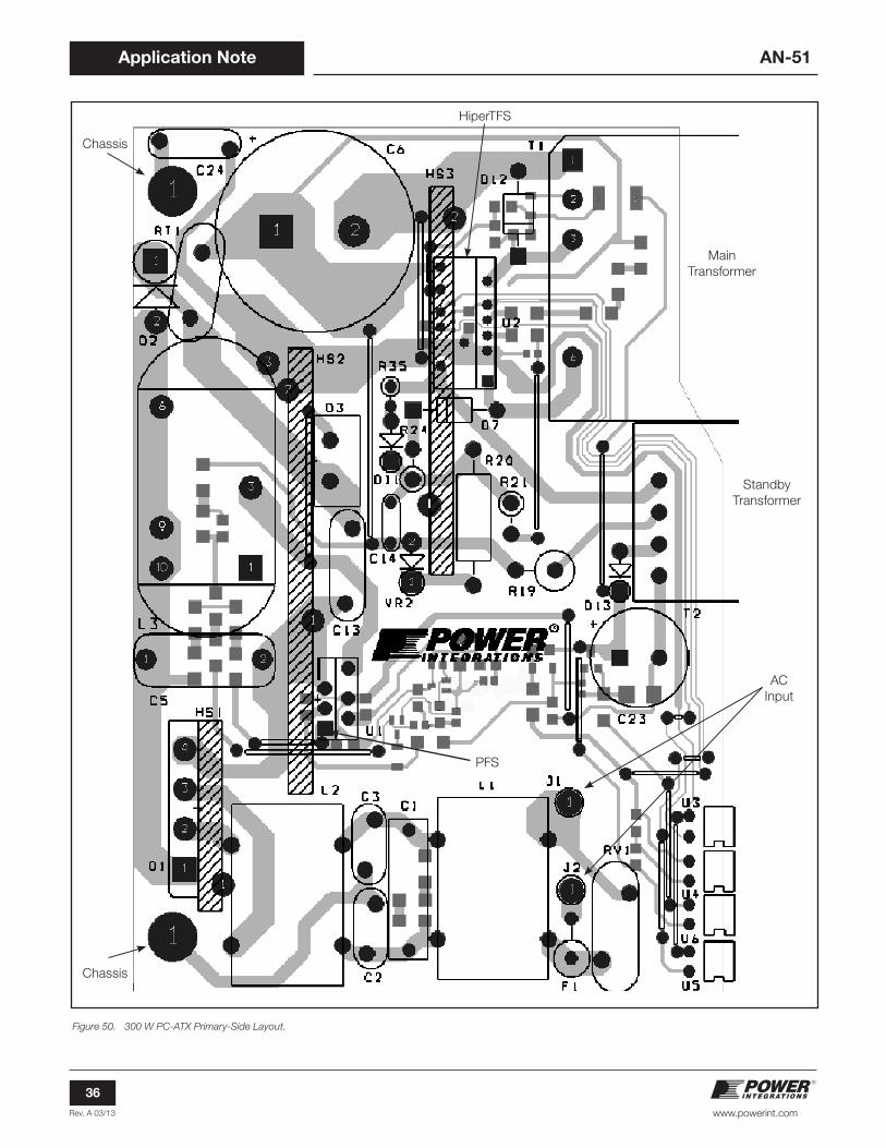
Rev. A 03/13
36
Application Note
www.powerint.com
AN-51
Figure 50. 300 W PC-ATX Primary-Side Layout.
MainTransformer
StandbyTransformer
ACInput
Chassis
Chassis
HiperTFS
PFS
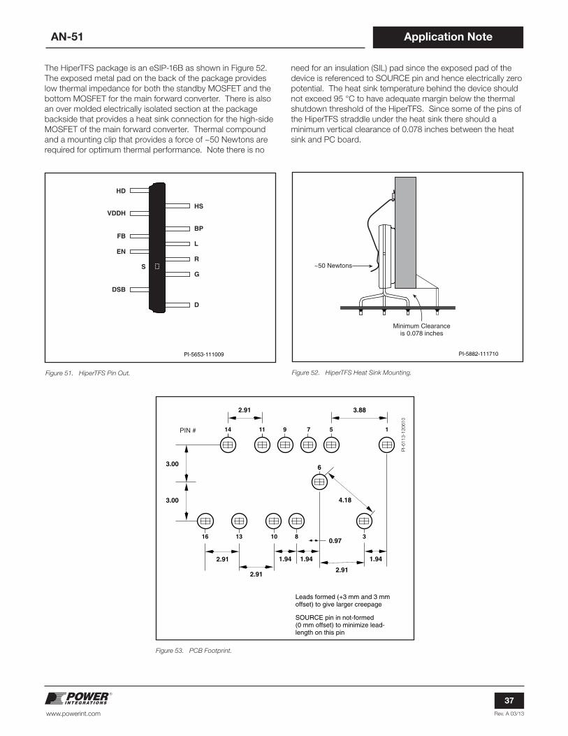
Rev. A 03/13
37
Application Note
www.powerint.com
AN-51
The HiperTFS package is an eSIP-16B as shown in Figure 52. The exposed metal pad on the back of the package provides low thermal impedance for both the standby MOSFET and the bottom MOSFET for the main forward converter. There is also an over molded electrically isolated section at the package backside that provides a heat sink connection for the high-side MOSFET of the main forward converter. Thermal compound and a mounting clip that provides a force of ~50 Newtons are required for optimum thermal performance. Note there is no
need for an insulation (SIL) pad since the exposed pad of the device is referenced to SOURCE pin and hence electrically zero potential. The heat sink temperature behind the device should not exceed 95 °C to have adequate margin below the thermal shutdown threshold of the HiperTFS. Since some of the pins of the HiperTFS straddle under the heat sink there should a minimum vertical clearance of 0.078 inches between the heat sink and PC board.
Figure 51. HiperTFS Pin Out. Figure 52. HiperTFS Heat Sink Mounting.
Figure 53. PCB Footprint.
PI-5882-111710
Minimum Clearanceis 0.078 inches
~50 Newtons
HD
VDDH
FB
EN
S
DSB
HS
BP
L
R
G
D
PI-5653-111009
PI-
6113
-120
610
Leads formed (+3 mm and 3 mm offset) to give larger creepage
SOURCE pin in not-formed(0 mm offset) to minimize lead-length on this pin
2.91
2.912.91
0.97
1.94 1.941.94
3.88
4.18
2.91
5 17911
6
3810
PIN #
3.00
3.00
14
16 13

Revision Notes Date
A Initial Release. 11/09/10
A Updated Figure 46. 03/20/13
For the latest updates, visit our website: www.powerint.comPower Integrations reserves the right to make changes to its products at any time to improve reliability or manufacturability. Power Integrations does not assume any liability arising from the use of any device or circuit described herein. POWER INTEGRATIONS MAKES NO WARRANTY HEREIN AND SPECIFICALLY DISCLAIMS ALL WARRANTIES INCLUDING, WITHOUT LIMITATION, THE IMPLIED WARRANTIES OF MERCHANTABILITY, FITNESS FOR A PARTICULAR PURPOSE, AND NON-INFRINGEMENT OF THIRD PARTY RIGHTS.
Patent InformationThe products and applications illustrated herein (including transformer construction and circuits external to the products) may be covered by one or more U.S. and foreign patents, or potentially by pending U.S. and foreign patent applications assigned to Power Integrations. A complete list of Power Integrations patents may be found at www.powerint.com. Power Integrations grants its customers a license under certain patent rights as set forth at http://www.powerint.com/ip.htm.
Life Support PolicyPOWER INTEGRATIONS PRODUCTS ARE NOT AUTHORIZED FOR USE AS CRITICAL COMPONENTS IN LIFE SUPPORT DEVICES OR SYSTEMS WITHOUT THE EXPRESS WRITTEN APPROVAL OF THE PRESIDENT OF POWER INTEGRATIONS. As used herein:
1. A Life support device or system is one which, (i) is intended for surgical implant into the body, or (ii) supports or sustains life, and (iii) whose failure to perform, when properly used in accordance with instructions for use, can be reasonably expected to result in significant injury or death to the user.
2. A critical component is any component of a life support device or system whose failure to perform can be reasonably expected to cause the failure of the life support device or system, or to affect its safety or effectiveness.
The PI logo, TOPSwitch, TinySwitch, LinkSwitch, LYTSwitch, DPA-Switch, PeakSwitch, CAPZero, SENZero, LinkZero, HiperPFS, HiperTFS, HiperLCS, Qspeed, EcoSmart, Clampless, E-Shield, Filterfuse, StakFET, PI Expert and PI FACTS are trademarks of Power Integrations, Inc. Other trademarks are property of their respective companies. ©2013, Power Integrations, Inc.
Power Integrations Worldwide Sales Support Locations
World Headquarters5245 Hellyer AvenueSan Jose, CA 95138, USA.Main: +1-408-414-9200Customer Service:Phone: +1-408-414-9665Fax: +1-408-414-9765e-mail: [email protected]
China (Shanghai)Rm 1601/1610, Tower 1,Kerry Everbright CityNo. 218 Tianmu Road West,Shanghai, P.R.C. 200070Phone: +86-21-6354-6323Fax: +86-21-6354-6325e-mail: [email protected]
China (ShenZhen)3rd Floor, Block A,Zhongtou International Business Center, No. 1061, Xiang Mei Rd,FuTian District, ShenZhen,China, 518040Phone: +86-755-8379-3243Fax: +86-755-8379-5828e-mail: [email protected]
GermanyLindwurmstrasse 11480337 MunichGermanyPhone: +49-895-527-39110Fax: +49-895-527-39200e-mail: [email protected]
India#1, 14th Main RoadVasanthanagarBangalore-560052 IndiaPhone: +91-80-4113-8020Fax: +91-80-4113-8023e-mail: [email protected]
ItalyVia Milanese 20, 3rd. Fl.20099 Sesto San Giovanni (MI)ItalyPhone: +39-024-550-8701Fax: +39-028-928-6009e-mail: [email protected]
JapanKosei Dai-3 Bldg. 2-12-11, Shin-Yokohama, Kohoku-ku Yokohama-shi Kanagwan 222-0033 JapanPhone: +81-45-471-1021Fax: +81-45-471-3717e-mail: [email protected]
KoreaRM 602, 6FLKorea City Air Terminal B/D, 159-6Samsung-Dong, Kangnam-Gu,Seoul, 135-728, KoreaPhone: +82-2-2016-6610Fax: +82-2-2016-6630e-mail: [email protected]
Singapore51 Newton Road#19-01/05 Goldhill PlazaSingapore, 308900Phone: +65-6358-2160Fax: +65-6358-2015e-mail: [email protected]
Taiwan5F, No. 318, Nei Hu Rd., Sec. 1Nei Hu Dist.Taipei 11493, Taiwan R.O.C.Phone: +886-2-2659-4570Fax: +886-2-2659-4550e-mail: [email protected]
Europe HQ1st Floor, St. James’s HouseEast Street, FarnhamSurrey GU9 7TJUnited KingdomPhone: +44 (0) 1252-730-141Fax: +44 (0) 1252-727-689e-mail: [email protected]
Applications HotlineWorld Wide +1-408-414-9660
Applications FaxWorld Wide +1-408-414-9760